Embed Size (px)
Citation preview

Schematic Driven Layout
Using the Design Mentor Graphics IC Studio
Santa Clara University
Department of Electrical Engineering
Prepared by Darshil Shah
Under Guidance of Dr. Samiha Mourad & Dr. Richard Sun Date of Last Revision: September 21, 2009
Table of Contents
1. Objective……………………………………………………………………... ……1
2. Setup & Preparation………………………………………………………………...1
3. Launching Design Architect-IC…………………………………………………….2
4. Schematic Entry…………………………………………………………………….3
5. Simulation…………………………………………………………………………..5
6. Creating Design Viewpoint………………………………………………………...5
7. Launching IC Station…………………………………………………………….....5
8. Schematic Driven Layout…………………………………………………………..7
9. DRC & LVS Check……………………………………………………………….13
1
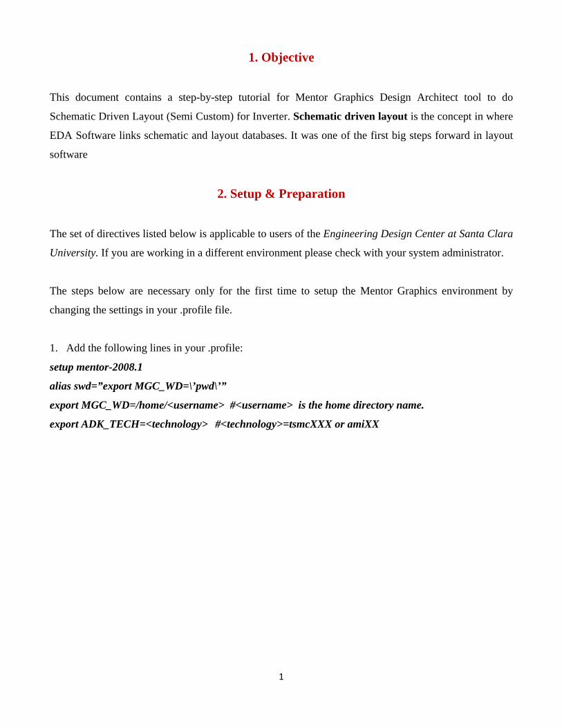
1. Objective
This document contains a step-by-step tutorial for Mentor Graphics Design Architect tool to do
Schematic Driven Layout (Semi Custom) for Inverter. Schematic driven layout is the concept in where
EDA Software links schematic and layout databases. It was one of the first big steps forward in layout
software
2. Setup & Preparation
The set of directives listed below is applicable to users of the Engineering Design Center at Santa Clara
University. If you are working in a different environment please check with your system administrator.
The steps below are necessary only for the first time to setup the Mentor Graphics environment by
changing the settings in your .profile file.
1. Add the following lines in your .profile:
setup mentor-2008.1
alias swd=”export MGC_WD=\’pwd\’”
export MGC_WD=/home/<username> #<username> is the home directory name.
export ADK_TECH=<technology> #<technology>=tsmcXXX or amiXX
2
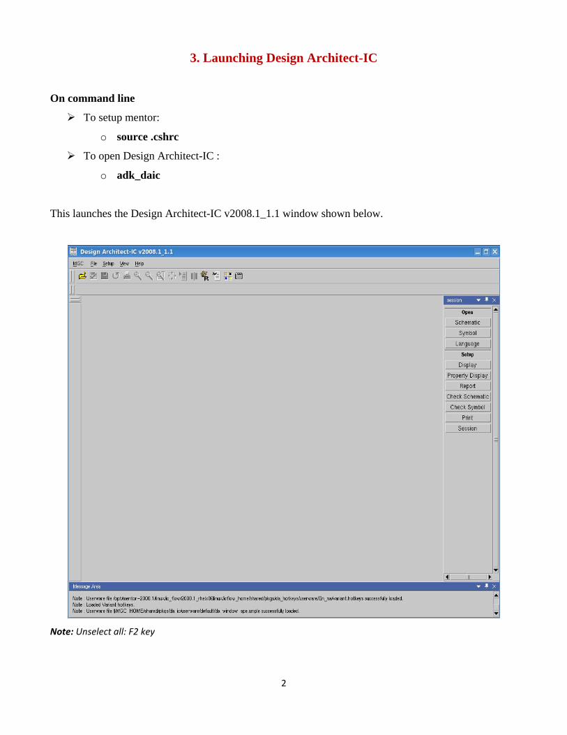
3. Launching Design Architect-IC
On command line
To setup mentor:
o source .cshrc
To open Design Architect-IC :
o adk_daic
This launches the Design Architect-IC v2008.1_1.1 window shown below.
Note: Unselect all: F2 key
3
4. Schematic Entry
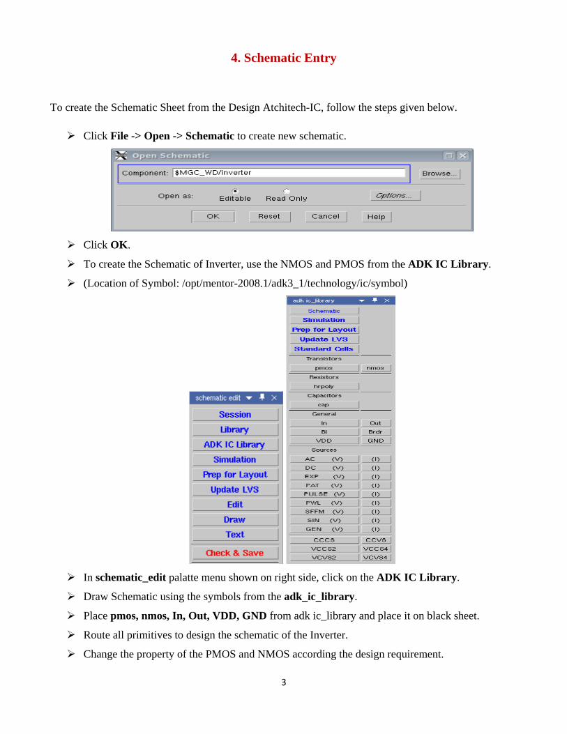
To create the Schematic Sheet from the Design Atchitech-IC, follow the steps given below.
Click File -> Open -> Schematic to create new schematic.
Click OK.
To create the Schematic of Inverter, use the NMOS and PMOS from the ADK IC Library.
(Location of Symbol: /opt/mentor-2008.1/adk3_1/technology/ic/symbol)
In schematic_edit palatte menu shown on right side, click on the ADK IC Library.
Draw Schematic using the symbols from the adk_ic_library.
Place pmos, nmos, In, Out, VDD, GND from adk ic_library and place it on black sheet.
Route all primitives to design the schematic of the Inverter.
Change the property of the PMOS and NMOS according the design requirement.

4
Click on Check & Save in the schematic_edit palette.
Open Miscellaneous -> Generate Symbol as shown in the figure:
5
Check & Save and close Symbol.
Click on the Prep for Layout on right side palatte, to create the view point.
Update LVS for create the netlist of the design.
Close the DA-IC.
5. Simulation
Use the Sources symbol from ADK IC Library. Simulation of the design can be done using the same
procedure as shown in Simulation PDF on http://www.dc.engr.scu.edu/mentortu/2007/dig_sim.pdf
6. Creating Design Viewpoint
On the command line:
adk_dve inverter -technology tsmc035
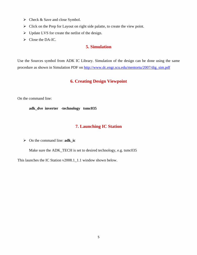
7. Launching IC Station
On the command line: adk_ic
Make sure the ADK_TECH is set to desired technology, e.g. tsmc035
This launches the IC Station v2008.1_1.1 window shown below.

6
Click Packages -> Acquire License.
Click on All Available License and Press OK

7
8. Schematic Driven Layout
Create New Schematic Driven Layout
Click on Create SDL in session palatte.
Logic Source: EDMM Viewpoint.
Path to Viewpoint: $MGC_WD/<design_name>/sdl
Cell Leaf Name: Root Component
Layout Directory: $MGC_WD
Process Name: $ADK/technology/ic/process/<tsmcXXX or amiXX>
Rule File: $ADK/technology/ic/process/<tsmcXXX.rules or amiXX.rules>
8
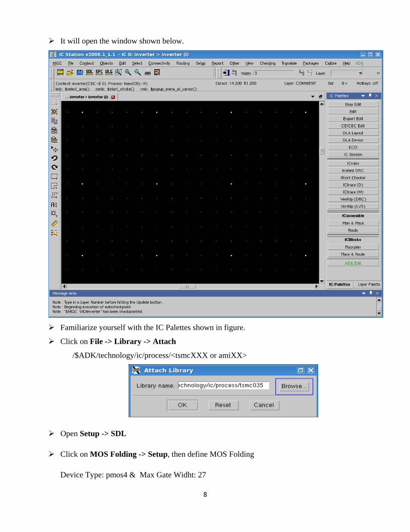
It will open the window shown below.
Familiarize yourself with the IC Palettes shown in figure.
Click on File -> Library -> Attach
/$ADK/technology/ic/process/<tsmcXXX or amiXX>
Open Setup -> SDL
Click on MOS Folding -> Setup, then define MOS Folding
Device Type: pmos4 & Max Gate Widht: 27
9
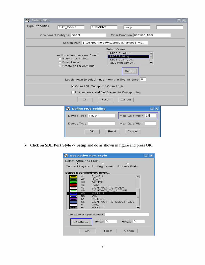
Click on SDL Port Style -> Setup and do as shown in figure and press OK.
10
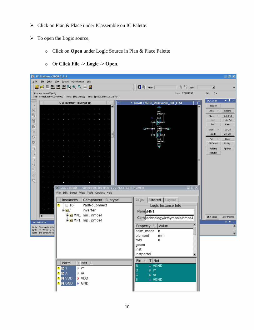
Click on Plan & Place under ICassemble on IC Palette.
To open the Logic source,
o Click on Open under Logic Source in Plan & Place Palette
o Or Click File -> Logic -> Open.
11
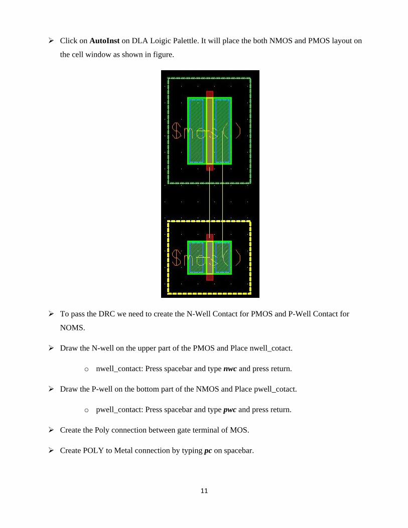
Click on AutoInst on DLA Loigic Palettle. It will place the both NMOS and PMOS layout on
the cell window as shown in figure.
To pass the DRC we need to create the N-Well Contact for PMOS and P-Well Contact for
NOMS.
Draw the N-well on the upper part of the PMOS and Place nwell_cotact.
o nwell_contact: Press spacebar and type nwc and press return.
Draw the P-well on the bottom part of the NMOS and Place pwell_cotact.
o pwell_contact: Press spacebar and type pwc and press return.
Create the Poly connection between gate terminal of MOS.
Create POLY to Metal connection by typing pc on spacebar.
12
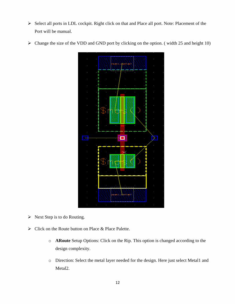
Select all ports in LDL cockpit. Right click on that and Place all port. Note: Placement of the
Port will be manual.
Change the size of the VDD and GND port by clicking on the option. ( width 25 and height 10)
Next Step is to do Routing.
Click on the Route button on Place & Place Palette.
o ARoute Setup Options: Click on the Rip. This option is changed according to the
design complexity.
o Direction: Select the metal layer needed for the design. Here just select Metal1 and
Metal2.

13
Press Run under the ARoute Commands.
Routing is done.
9. DRC & LVS Check
DRC & LVS Rule File:
/applications/mentor/2008.1/adk3_1/technology/ic/process/tsmcXXX.rules
DRC and LVS of the design can be done using the same procedure as shown in DRC & LVS
PDF on http://www.dc.engr.scu.edu/mentortu/2007/dig_ver.pdf