1
Department of EECS University of California, Berkeley
EECS 105 Spring 2004, Lecture 21
Lecture 21: BJTs(Bipolar Junction Transistors)
Prof J. S. Smith
Department of EECS University of California, Berkeley
EECS 105 Spring 2004, Lecture 21 Prof. J. S. Smith
Context
In Monday’s lecture, we discussed minority injection in forward biased PN junctions.
Today we will discuss three terminal devices which use this effect for amplification, called:BJTs (Bipolar Junction Transistors)
2
Department of EECS University of California, Berkeley
EECS 105 Spring 2004, Lecture 21 Prof. J. S. Smith
Reading
Today’s lecture will covering chapter 7, Bipolar Junction Transistors (BJT’s)
Next , we will start looking at amplifiers, chapter 8 in the text.
Department of EECS University of California, Berkeley
EECS 105 Spring 2004, Lecture 21 Prof. J. S. Smith
Lecture Outline
Review of minority current injection in PN DiodeThe BJT (7.1)BJT Physics (7.2)BJT Ebers-Moll Equations (7.3)BJT Small-Signal Model
3
Department of EECS University of California, Berkeley
EECS 105 Spring 2004, Lecture 21 Prof. J. S. Smith
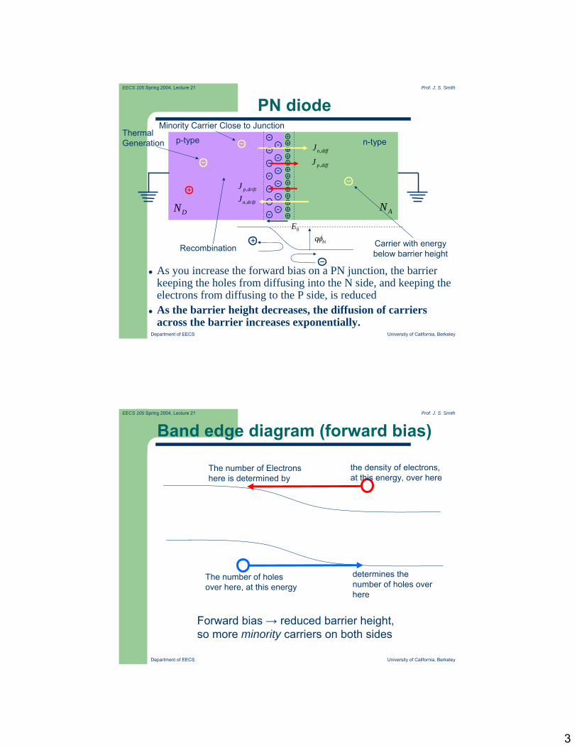
PN diode
As you increase the forward bias on a PN junction, the barrier keeping the holes from diffusing into the N side, and keeping the electrons from diffusing to the P side, is reducedAs the barrier height decreases, the diffusion of carriers across the barrier increases exponentially.
p-type n-type
DN AN
---
-
---
------
+++++++++++++
0E
biqφ
,p diffJ
,p driftJ
,n diffJ
,n driftJ
−
−
+
+
−
−
ThermalGeneration
Recombination Carrier with energybelow barrier height
Minority Carrier Close to Junction
Department of EECS University of California, Berkeley
EECS 105 Spring 2004, Lecture 21 Prof. J. S. Smith
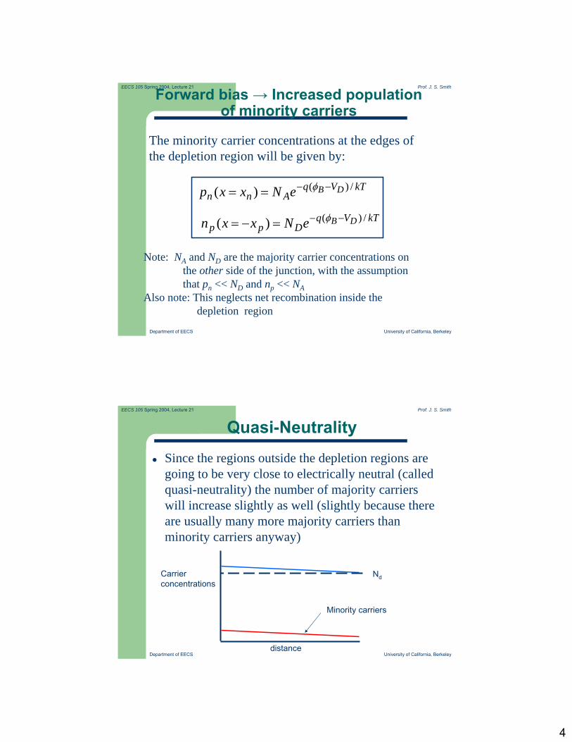
Band edge diagram (forward bias)
the density of electrons,at this energy, over here
The number of Electronshere is determined by
The number of holesover here, at this energy
determines thenumber of holes overhere
Forward bias → reduced barrier height, so more minority carriers on both sides
4
Department of EECS University of California, Berkeley
EECS 105 Spring 2004, Lecture 21 Prof. J. S. Smith
Forward bias → Increased population of minority carriers
The minority carrier concentrations at the edges of the depletion region will be given by:
kTVqAnn
DBeNxxp /)()( −−== φ
kTVqDpp
DBeNxxn /)()( −−=−= φ
Note: NA and ND are the majority carrier concentrations onthe other side of the junction, with the assumption that pn << ND and np << NA
Also note: This neglects net recombination inside thedepletion region
Department of EECS University of California, Berkeley
EECS 105 Spring 2004, Lecture 21 Prof. J. S. Smith
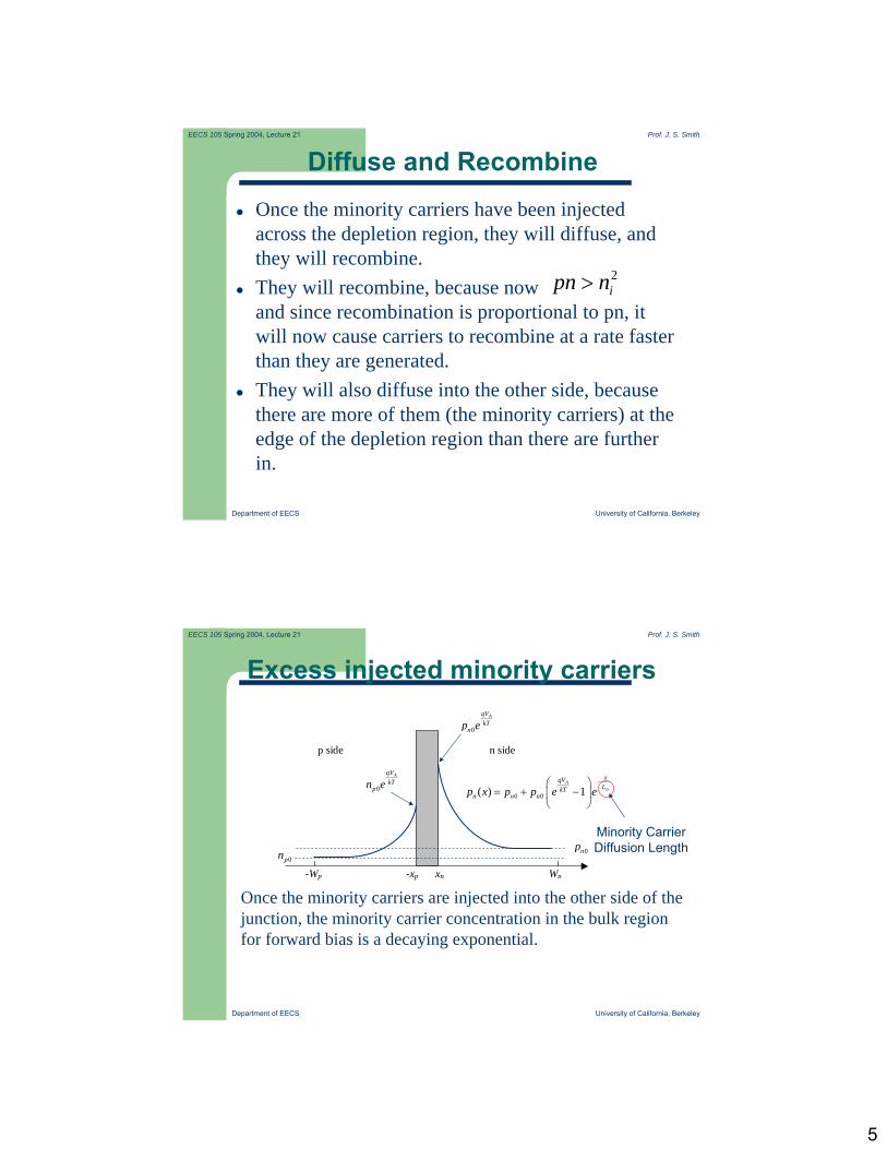
Quasi-Neutrality
Since the regions outside the depletion regions are going to be very close to electrically neutral (called quasi-neutrality) the number of majority carriers will increase slightly as well (slightly because there are usually many more majority carriers than minority carriers anyway)
Carrier concentrations
distance
Nd
Minority carriers
5
Department of EECS University of California, Berkeley
EECS 105 Spring 2004, Lecture 21 Prof. J. S. Smith
Diffuse and Recombine
Once the minority carriers have been injected across the depletion region, they will diffuse, and they will recombine.They will recombine, because now and since recombination is proportional to pn, it will now cause carriers to recombine at a rate faster than they are generated.They will also diffuse into the other side, because there are more of them (the minority carriers) at the edge of the depletion region than there are further in.
2inpn >
Department of EECS University of California, Berkeley
EECS 105 Spring 2004, Lecture 21 Prof. J. S. Smith
Excess injected minority carriers
Once the minority carriers are injected into the other side of the junction, the minority carrier concentration in the bulk region for forward bias is a decaying exponential.
p side n side
-Wp Wn xn -xp
0
AqVkT
np e
0 0( ) 1A
p
xqVLkT
n n np x p p e e−⎛ ⎞
= + −⎜ ⎟⎝ ⎠
0np0pn
0
AqVkT
pn e
Minority CarrierDiffusion Length
6
Department of EECS University of California, Berkeley
EECS 105 Spring 2004, Lecture 21 Prof. J. S. Smith
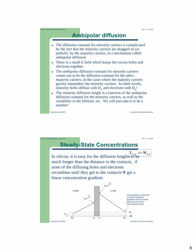
Ambipolar diffusionThe diffusion constant for minority carriers is complicated by the fact that the minority carriers are dragged on (or pulled!) by the majority carriers, in a mechanism called ambipolar diffusion There is a small E field which keeps the excess holes and electrons together.The ambipolar diffusion constant for minority carriers comes out to be the diffusion constant for the other, majority carriers, in the cases where the majority carriers greatly outnumber the minority carriers. In other words, minority holes diffuse with Dn and electrons with Dp!The minority diffusion length is a function of the ambipolardiffusion constant for the minority carriers, as well as the variability in the lifetime, etc. We will just take it to be a number!
Department of EECS University of California, Berkeley
EECS 105 Spring 2004, Lecture 21 Prof. J. S. Smith
Steady-State Concentrations
In silicon, it is easy for the diffusion lengths to be much longer than the distance to the contacts, if none of the diffusing holes and electrons recombine until they get to the contacts get a linear concentration gradient.
p side n side
-Wp Wn xn -xp
0
AqVkT
np e
0np0pn
0
AqVkT
pn e
, ,n p n pL W>>
The population is assumedto be the equilibriumpopulation at the contactsbecause of the manytraps (defects) there
7
Department of EECS University of California, Berkeley
EECS 105 Spring 2004, Lecture 21 Prof. J. S. Smith
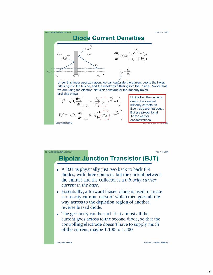
Diode Current Densities
0 1A
p
qVpdiff n kT
n n ppx x
dn DJ qD q n edx W
=−
⎛ ⎞= ≈ −⎜ ⎟
⎝ ⎠
0 0( )( )
AqVkT
p p p
p p
dn n e nx
dx x W−
≈− − −
p side n side
-Wp Wn xn -xp
0
AqVkT
np e
0np
0pn
0
AqVkT
pn e
0 1A
n
qVpdiff n kT
p p nx x n
DdpJ qD q p edx W=
⎛ ⎞= − ≈ − −⎜ ⎟
⎝ ⎠
2
0i
pa
nnN
=
Under this linear approximation, we can calculate the current due to the holes diffusing into the N side, and the electrons diffusing into the P side. Notice thatwe are using the electron diffusion constant for the minority holes, and visa versa.
Notice that the currentsdue to the injectedMinority carriers on Each side are not equal,But are proportionalTo the carrier concentrations
Department of EECS University of California, Berkeley
EECS 105 Spring 2004, Lecture 21 Prof. J. S. Smith
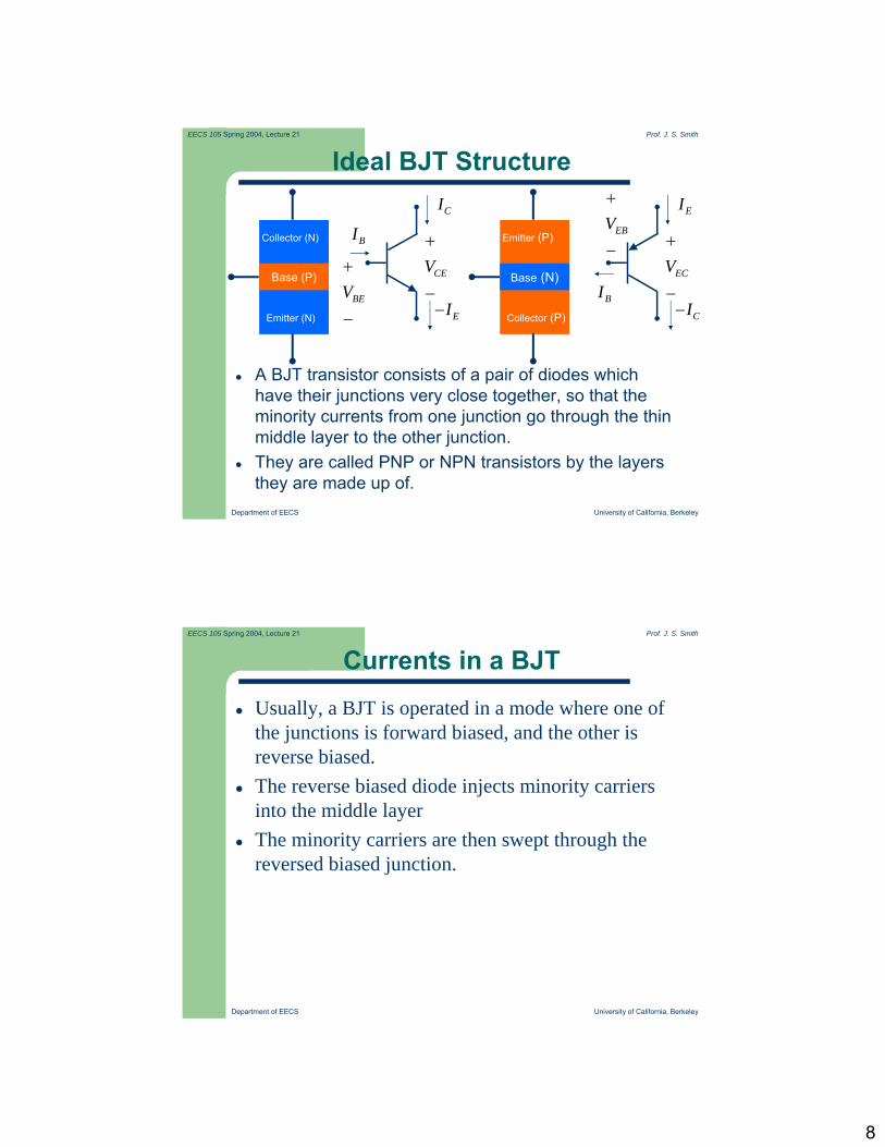
Bipolar Junction Transistor (BJT)A BJT is physically just two back to back PN diodes, with three contacts, but the current between the emitter and the collector is a minority carrier current in the base.Essentially, a forward biased diode is used to create a minority current, most of which then goes all the way across to the depletion region of another, reverse biased diode.The geometry can be such that almost all the current goes across to the second diode, so that the controlling electrode doesn’t have to supply much of the current, maybe 1:100 to 1:400
8
Department of EECS University of California, Berkeley
EECS 105 Spring 2004, Lecture 21 Prof. J. S. Smith
Ideal BJT Structure
A BJT transistor consists of a pair of diodes which have their junctions very close together, so that the minority currents from one junction go through the thin middle layer to the other junction.They are called PNP or NPN transistors by the layers they are made up of.
Base (P)
Collector (N)
Emitter (N)
CI
BI
EI−BEV+
−
CEV+
−Base (N)
Emitter (P)
Collector (P)
EI
BICI−
EBV+
−ECV+
−
Department of EECS University of California, Berkeley
EECS 105 Spring 2004, Lecture 21 Prof. J. S. Smith
Currents in a BJT
Usually, a BJT is operated in a mode where one of the junctions is forward biased, and the other is reverse biased. The reverse biased diode injects minority carriers into the middle layerThe minority carriers are then swept through the reversed biased junction.
9
Department of EECS University of California, Berkeley
EECS 105 Spring 2004, Lecture 21 Prof. J. S. Smith
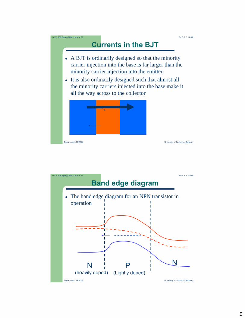
Currents in the BJT
A BJT is ordinarily designed so that the minority carrier injection into the base is far larger than the minority carrier injection into the emitter.It is also ordinarily designed such that almost all the minority carriers injected into the base make it all the way across to the collector
Department of EECS University of California, Berkeley
EECS 105 Spring 2004, Lecture 21 Prof. J. S. Smith
Band edge diagram
The band edge diagram for an NPN transistor in operation
N(heavily doped)
P(Lightly doped)
N
10
Department of EECS University of California, Berkeley
EECS 105 Spring 2004, Lecture 21 Prof. J. S. Smith
Current controlled
So the current is determined by the minority current across the emitter-base junction
But since the majority of the minority current goes right through the base to the collector:
And so the amount of current that must be supplied by the base is small compared to the current controlled:
C EI I≈ −
C BI I>>
BEqVkT
C SI I e≈
Department of EECS University of California, Berkeley
EECS 105 Spring 2004, Lecture 21 Prof. J. S. Smith
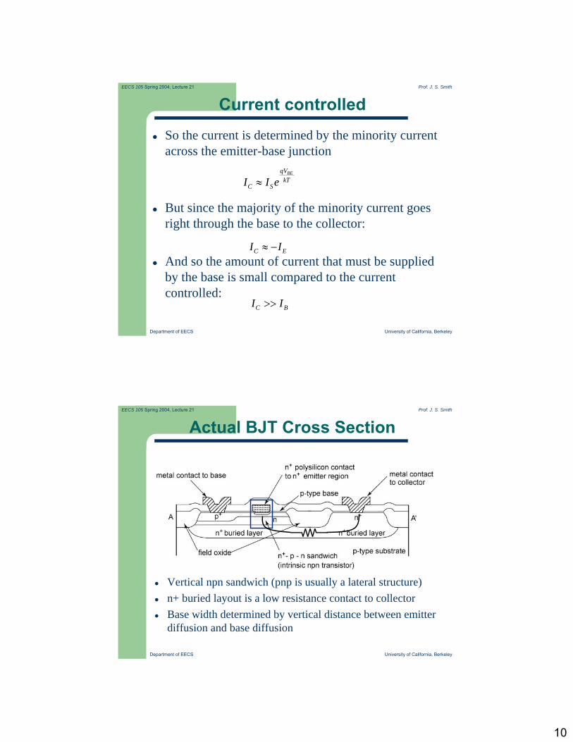
Actual BJT Cross Section
Vertical npn sandwich (pnp is usually a lateral structure)n+ buried layout is a low resistance contact to collectorBase width determined by vertical distance between emitter diffusion and base diffusion
11
Department of EECS University of California, Berkeley
EECS 105 Spring 2004, Lecture 21 Prof. J. S. Smith
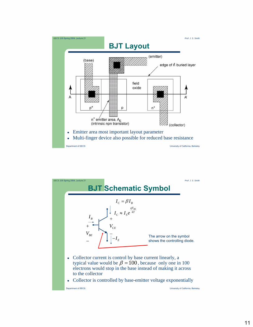
BJT Layout
Emitter area most important layout parameterMulti-finger device also possible for reduced base resistance
Department of EECS University of California, Berkeley
EECS 105 Spring 2004, Lecture 21 Prof. J. S. Smith
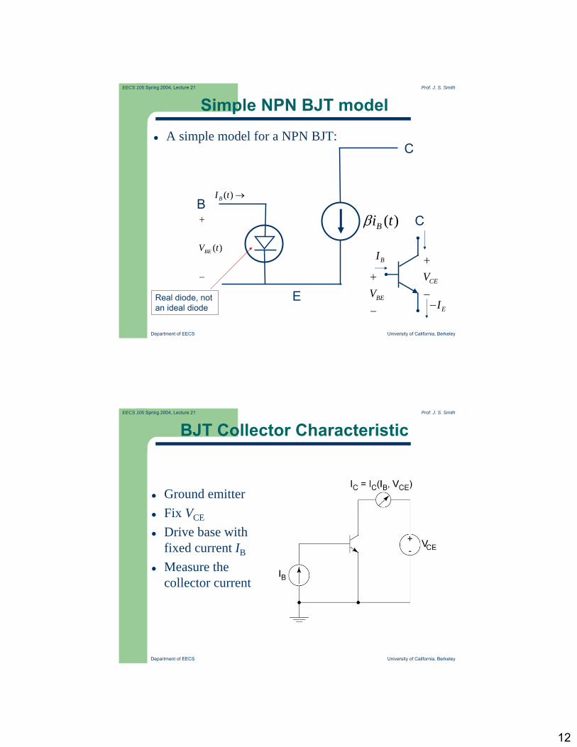
BJT Schematic Symbol
Collector current is control by base current linearly, a typical value would be , because only one in 100electrons would stop in the base instead of making it across to the collectorCollector is controlled by base-emitter voltage exponentially
BI
EI−BEV+
−
CEV+
−
BEqVkT
C SI I e≈
C BI Iβ=
The arrow on the symbol shows the controlling diode.
100=β
12
Department of EECS University of California, Berkeley
EECS 105 Spring 2004, Lecture 21 Prof. J. S. Smith
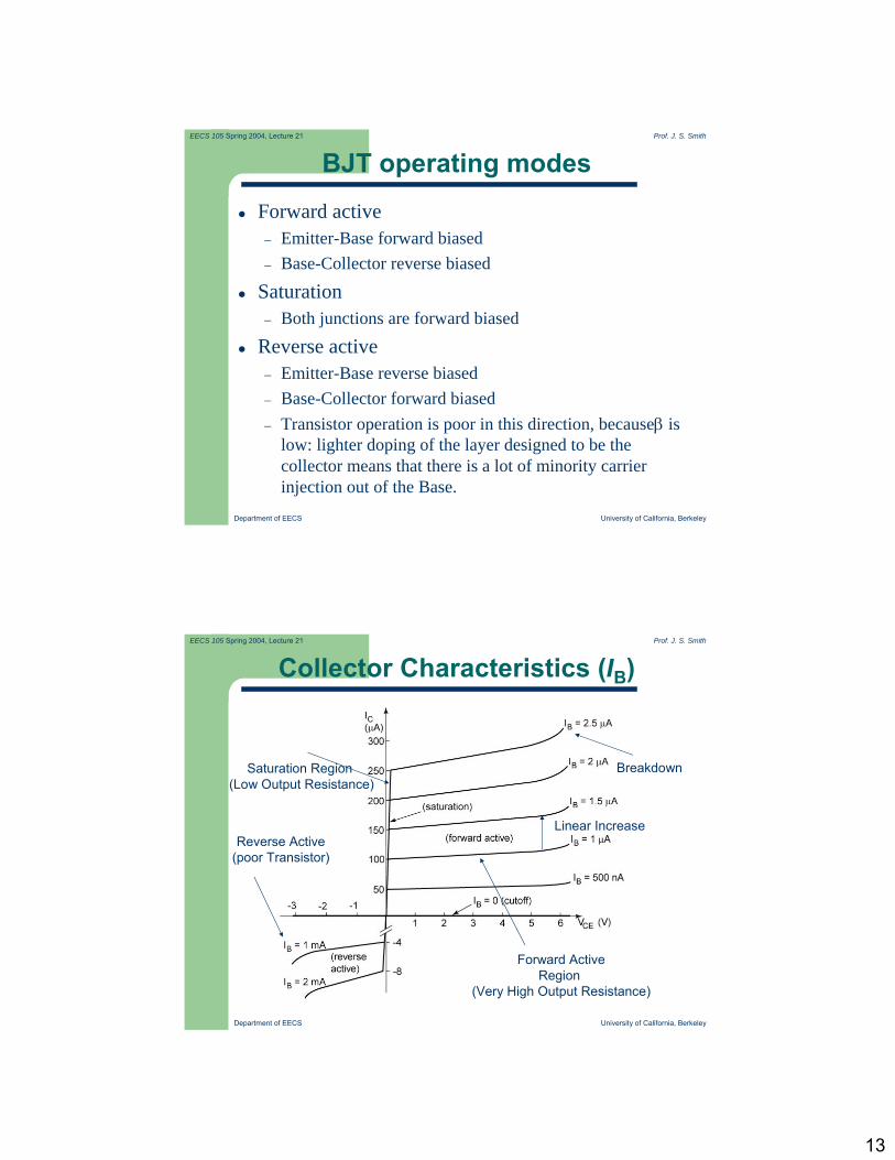
Simple NPN BJT model
A simple model for a NPN BJT:
→)(tIB
−
+
)(tVBE
)(tiBβB
E
C
Real diode, not an ideal diode
BI
EI−BEV+
−
CEV+
−
C
Department of EECS University of California, Berkeley
EECS 105 Spring 2004, Lecture 21 Prof. J. S. Smith
BJT Collector Characteristic
Ground emitterFix VCE
Drive base with fixed current IB
Measure the collector current
13
Department of EECS University of California, Berkeley
EECS 105 Spring 2004, Lecture 21 Prof. J. S. Smith
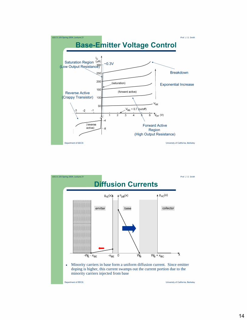
BJT operating modes
Forward active– Emitter-Base forward biased– Base-Collector reverse biased
Saturation– Both junctions are forward biased
Reverse active– Emitter-Base reverse biased– Base-Collector forward biased– Transistor operation is poor in this direction, becauseβ is
low: lighter doping of the layer designed to be the collector means that there is a lot of minority carrier injection out of the Base.
Department of EECS University of California, Berkeley
EECS 105 Spring 2004, Lecture 21 Prof. J. S. Smith
Collector Characteristics (IB)
Forward ActiveRegion
(Very High Output Resistance)
Saturation Region (Low Output Resistance)
Reverse Active(poor Transistor)
Breakdown
Linear Increase
14
Department of EECS University of California, Berkeley
EECS 105 Spring 2004, Lecture 21 Prof. J. S. Smith
Base-Emitter Voltage Control
Exponential Increase
Forward ActiveRegion
(High Output Resistance)
Reverse Active(Crappy Transistor)
Saturation Region (Low Output Resistance)
~0.3V
Breakdown
Department of EECS University of California, Berkeley
EECS 105 Spring 2004, Lecture 21 Prof. J. S. Smith
Diffusion Currents
Minority carriers in base form a uniform diffusion current. Since emitter doping is higher, this current swamps out the current portion due to the minority carriers injected from base
15
Department of EECS University of California, Berkeley
EECS 105 Spring 2004, Lecture 21 Prof. J. S. Smith
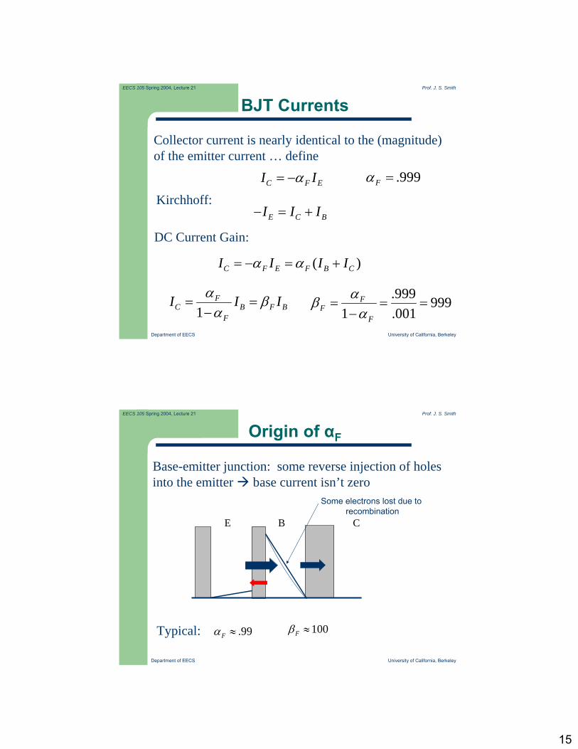
BJT Currents
C F EI Iα= −
Collector current is nearly identical to the (magnitude)of the emitter current … define
Kirchhoff: E C BI I I− = +
DC Current Gain:
( )C F E F B CI I I Iα α= − = +
1F
C B F BF
I I Iα βα
= =−
.999Fα =
.999 9991 .001
FF
F
αβα
= = =−
Department of EECS University of California, Berkeley
EECS 105 Spring 2004, Lecture 21 Prof. J. S. Smith
Origin of αF
Base-emitter junction: some reverse injection of holes into the emitter base current isn’t zero
E B C
Typical:
Some electrons lost due to recombination
.99Fα ≈ 100Fβ ≈
16
Department of EECS University of California, Berkeley
EECS 105 Spring 2004, Lecture 21 Prof. J. S. Smith
Collector Current
Diffusion of electrons across base results in
0BEqV
p n pBdiff kTn n
B
dn qD nJ qD e
dx W⎛ ⎞
= = ⎜ ⎟⎝ ⎠
BEqVkT
C SI I e=
0n pB ES
B
qD n AI
W⎛ ⎞
= ⎜ ⎟⎝ ⎠
Department of EECS University of California, Berkeley
EECS 105 Spring 2004, Lecture 21 Prof. J. S. Smith
Base Current
In silicon, recombination of carriers in the basecan usually be neglected, so the base current is mostly due to minority injection into the emitter.Diffusion of holes across emitter results in
0 1BEqV
p nEdiff nE kTp p
E
qD pdpJ qD edx W
⎛ ⎞⎛ ⎞= − = −⎜ ⎟⎜ ⎟
⎝ ⎠⎝ ⎠
0 1BEqV
p nE E kTB
E
qD p AI e
W⎛ ⎞⎛ ⎞
= −⎜ ⎟⎜ ⎟⎝ ⎠⎝ ⎠
17
Department of EECS University of California, Berkeley
EECS 105 Spring 2004, Lecture 21 Prof. J. S. Smith
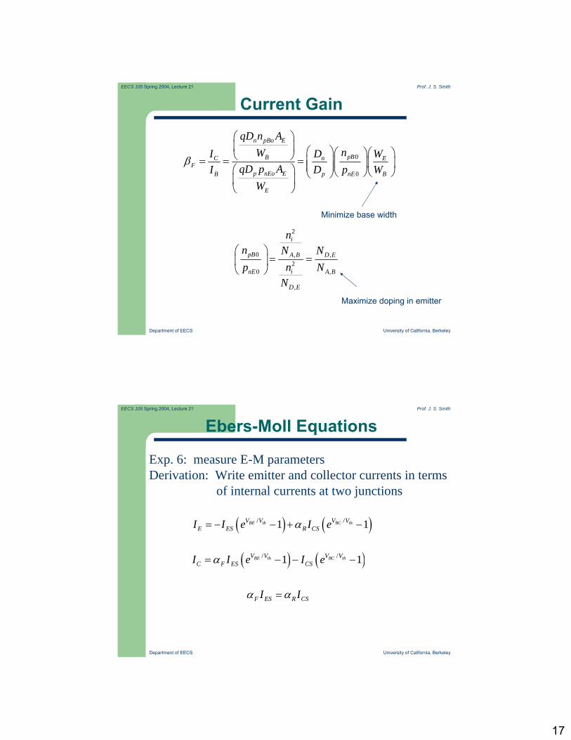
Current Gain
0
0
n pBo E
pBBC n EF
p nEo EB p nE B
E
qD n AnWI D W
qD p AI D p WW
β
⎛ ⎞⎜ ⎟ ⎛ ⎞⎛ ⎞⎛ ⎞⎝ ⎠= = = ⎜ ⎟⎜ ⎟⎜ ⎟⎜ ⎟⎛ ⎞ ⎝ ⎠⎝ ⎠⎝ ⎠⎜ ⎟⎝ ⎠
2
0 , ,2
0 ,
,
i
pB A B D E
inE A B
D E
nn N N
np NN
⎛ ⎞= =⎜ ⎟
⎝ ⎠
Minimize base width
Maximize doping in emitter
Department of EECS University of California, Berkeley
EECS 105 Spring 2004, Lecture 21 Prof. J. S. Smith
Ebers-Moll Equations
Exp. 6: measure E-M parametersDerivation: Write emitter and collector currents in terms
of internal currents at two junctions
( ) ( )/ /1 1BE th BC thV V V VE ES R CSI I e I eα= − − + −
( ) ( )/ /1 1BE th BC thV V V VC F ES CSI I e I eα= − − −
F ES R CSI Iα α=
18
Department of EECS University of California, Berkeley
EECS 105 Spring 2004, Lecture 21 Prof. J. S. Smith
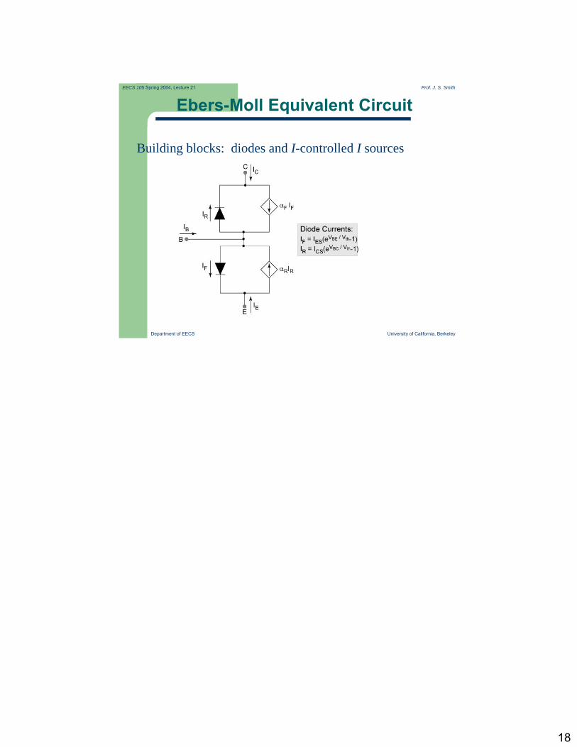
Ebers-Moll Equivalent Circuit
Building blocks: diodes and I-controlled I sources
Recommended