Latent Damage FromSingle-Event Latchup
Heidi N. Becker, Tetsuo F. Miyahira
and Allan H. JohnstonJet Propulsion Laboratory
California Institute of Technology
2002 Single Event Effects Symposium
The research in this presentation was carried out by the Jet Propulsion Laboratory, California Institute of Technology under
contract with the National Aeronautics and Space Administration (NASA) Code AE.
2
Outline
• Initial Interest & Observations
• Data
• Analysis
• Conclusions
3
Initial Interest: Catastrophic SEL
• How are SEL failures related to device properties?
• AD9260 failed from latchup during heavy ion testing
• Laser-induced SEL testing at the Aerospace Corp.- induce latchup with laser pulses- observe latchup equilibrium currents- monitor device functionality- observe irradiated area on the die through CCD camera/video monitor
4
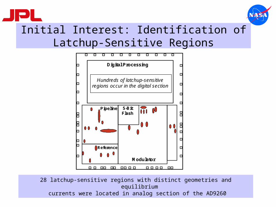
Initial Interest: Identification of Latchup-Sensitive Regions
28 latchup-sensitive regions with distinct geometries and equilibrium currents were located in analog section of the AD9260
Digital Processing
5-BitFlash
Modulator
Reference
Pipeline
Hundreds of latchup-sensitiveregions occur in the digital section
5
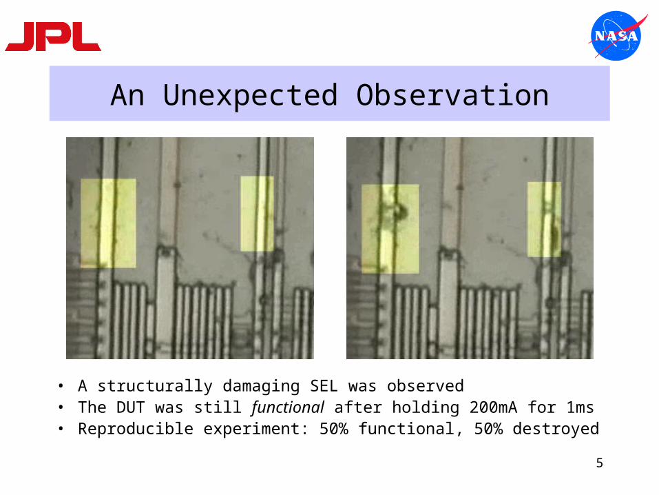
An Unexpected Observation
• A structurally damaging SEL was observed• The DUT was still functional after holding 200mA for 1ms• Reproducible experiment: 50% functional, 50% destroyed

6
Data: CMOS Devices Studied for SEL-Induced Structural Damage
CMOS Device
Device Type
Manufacturer Latent Damage
AD9260 ADC Analog Devices Yes
AD9240 ADC Analog Devices No
ADC10321 ADC NSC Yes
CAR/CPPX1T-A7BR
Oscillator Cardinal/Cypress Hybrid
Yes
LTC1799 Oscillator Linear Technology No
ADSP2100 DSP Analog Devices No
7
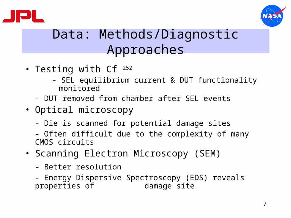
Data: Methods/Diagnostic Approaches
• Testing with Cf 252
- SEL equilibrium current & DUT functionality monitored- DUT removed from chamber after SEL events
• Optical microscopy
- Die is scanned for potential damage sites
- Often difficult due to the complexity of many CMOS circuits
• Scanning Electron Microscopy (SEM)
- Better resolution
- Energy Dispersive Spectroscopy (EDS) reveals properties of damage site
8
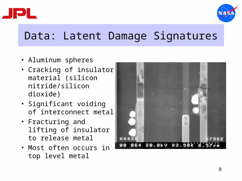
Data: Latent Damage Signatures
• Aluminum spheres
• Cracking of insulator material (silicon nitride/silicon dioxide)
• Significant voiding of interconnect metal
• Fracturing and lifting of insulator to release metal
• Most often occurs in top level metal
9
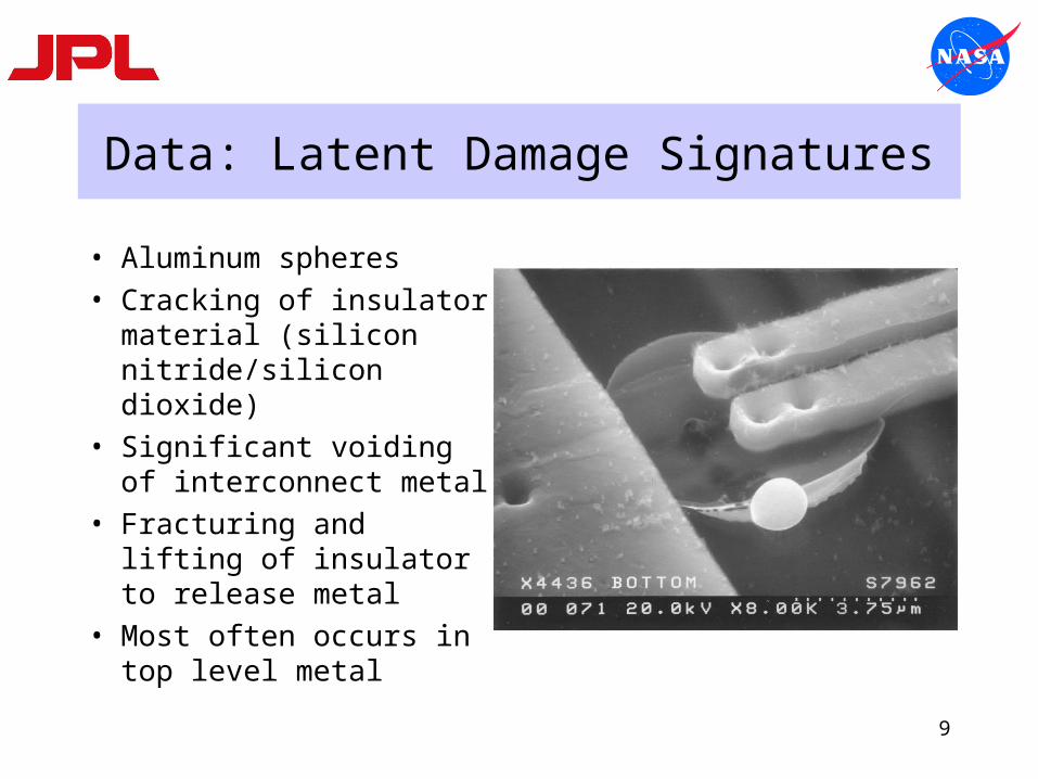
Data: Latent Damage Signatures
• Aluminum spheres
• Cracking of insulator material (silicon nitride/silicon dioxide)
• Significant voiding of interconnect metal
• Fracturing and lifting of insulator to release metal
• Most often occurs in top level metal
10
Data: Key Parameters of Latent Damage
• Minimum Current Density: 107A/cm2
- Ranged from 107-108A/cm2
- Based on latchup equilibrium current drawn by DUT & cross-sectional area of damaged interconnect
• Cross-sectional area of damaged interconnect: 1-10µm2
• All tested devices of the same model were damaged in the same area on the die
- Indicates damage is not caused by fabrication defects
• Time scale: 60µs – 18ms• More extreme/violent than electromigration (5x10⁵A/cm2)
11
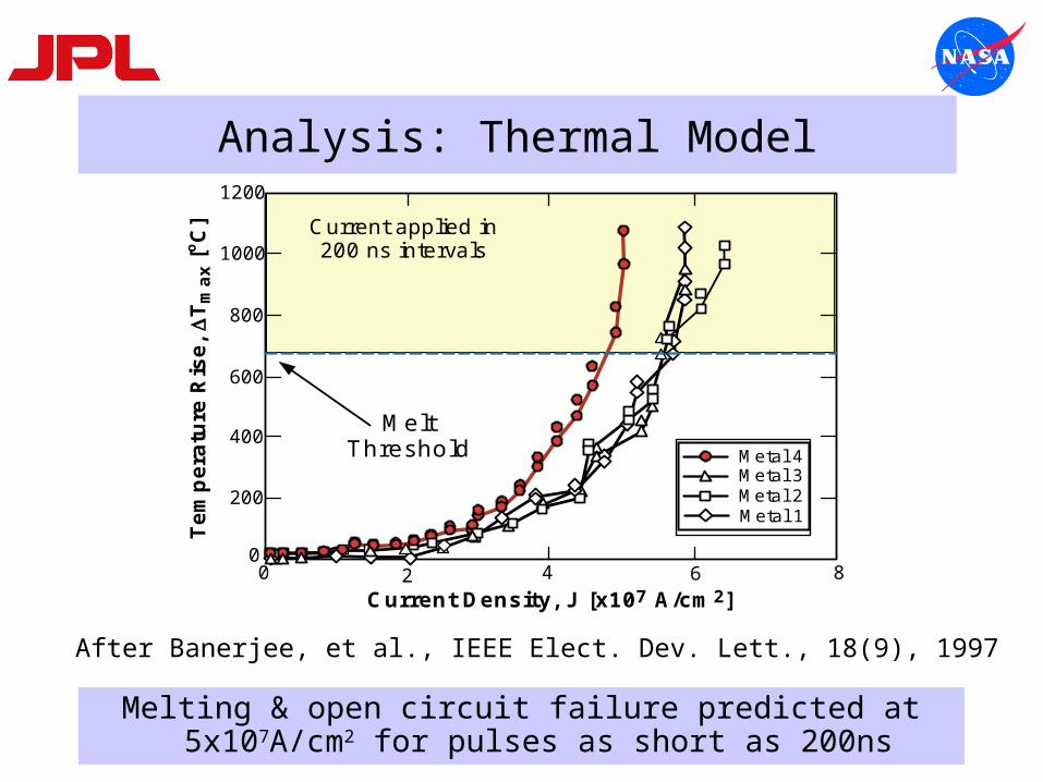
Analysis: Thermal Model
Melting & open circuit failure predicted at 5x10⁷A/cm2 for pulses as short as 200ns
Metal 2Metal 3
Metal 1
Metal 4
Temperature
Rise,DTmax[oC]
0 2 80
1200
4 6
1000
800
600
400
200
Current Density, J [x107 A/cm2]
Current applied in200 ns intervals
MeltThresho ld
After Banerjee, et al., IEEE Elect. Dev. Lett., 18(9), 1997
12
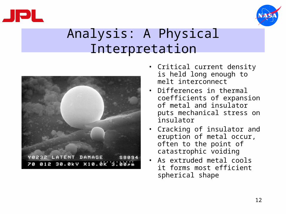
Analysis: A Physical Interpretation
• Critical current density is held long enough to melt interconnect
• Differences in thermal coefficients of expansion of metal and insulator puts mechanical stress on insulator
• Cracking of insulator and eruption of metal occur, often to the point of catastrophic voiding
• As extruded metal cools it forms most efficient spherical shape
13
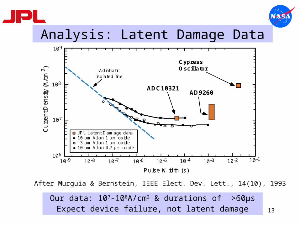
Analysis: Latent Damage Data
Our data: 107-108A/cm2 & durations of >60µsExpect device failure, not latent damage
After Murguia & Bernstein, IEEE Elect. Dev. Lett., 14(10), 1993
JPL Latent Damage data10 µm Al on 1 µm oxide3 µm Al on 1 µm oxide10 µm Al on 0.7 µm oxide
Pulse W idth (s)
CurrentDensity(A/cm2)
10-9 10-610-7 10-5 10-4 10-3 10-210-8106
107
108
109
AD9260ADC10321
CypressOscillator
10-1
Adiabaticisolated line
14
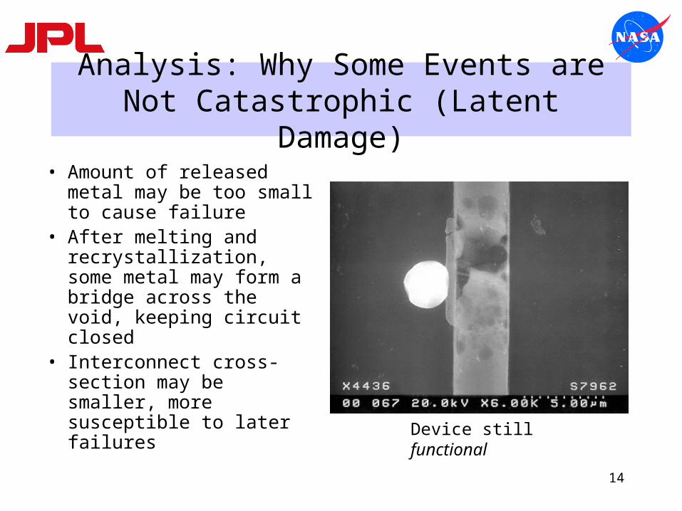
Analysis: Why Some Events are Not Catastrophic (Latent Damage)
• Amount of released metal may be too small to cause failure
• After melting and recrystallization, some metal may form a bridge across the void, keeping circuit closed
• Interconnect cross-section may be smaller, more susceptible to later failures Device still functional
15
Conclusions: Impact on Future SEL Testing
• Unless you look for latent damage, you don’t know it’s there
• Permanent structural damage may eventually cause device failure
• Latchup circumvention should address concerns about latent damage
• The semiconductor industry is moving toward using more levels of metal and smaller interconnects
=> next generation devices may exhibita higher rate of latent damage
16
Acknowledgements
Stephen D. LaLumondiere
Steven C. Moss
The Aerospace Corporation
Kenneth C. Evans
Jet Propulsion Laboratory
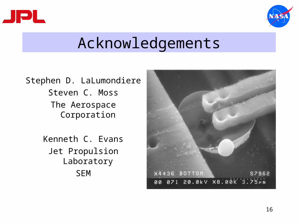
SEM
Recommended