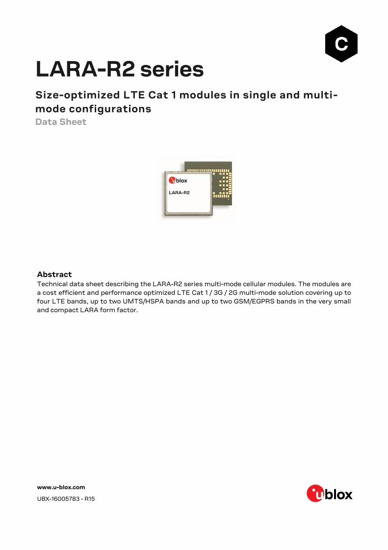
LARA-R2 series Size-optimized LTE Cat 1 modules in single and multi-
mode configurations Data Sheet
Abstract Technical data sheet describing the LARA-R2 series multi-mode cellular modules. The modules are
a cost efficient and performance optimized LTE Cat 1 / 3G / 2G multi-mode solution covering up to
four LTE bands, up to two UMTS/HSPA bands and up to two GSM/EGPRS bands in the very small
and compact LARA form factor.
www.u-blox.com
UBX-16005783 - R15
LARA-R2 series - Data Sheet
UBX-16005783 - R15 Page 2 of 48
Document Information
Title LARA-R2 series
Subtitle Size-optimized LTE Cat 1 modules in single and multi-mode configurations
Document type Data Sheet
Document number UBX-16005783
Revision and date R15 27-May-2018
Disclosure Restriction
Product status Corresponding content status
Functional Sample Draft For functional testing. Revised and supplementary data will be published later.
In Development /
Prototype
Objective Specification Target values. Revised and supplementary data will be published later.
Engineering Sample Advance Information Data based on early testing. Revised and supplementary data will be published later.
Initial Production Early Production Information Data from product verification. Revised and supplementary data may be published later.
Mass Production /
End of Life
Production Information Document contains the final product specification.
This document applies to the following products:
Product name Type number Modem version Application version PCN reference Product status
LARA-R202 LARA-R202-02B-00 30.42 A01.00 UBX-17057959 End of Life
LARA-R202-02B-01 30.42 A01.01 UBX-18018067 Initial Production
LARA-R203 LARA-R203-02B-00 30.39 A01.00 UBX-17048311 End of Life
LARA-R203-02B-01 30.39 A01.02 UBX-18018067 Initial Production
LARA-R204 LARA-R204-02B-00 31.34 A01.00 UBX-17012269 End of Life
LARA-R204-02B-01 31.35 A01.03 UBX-18013471 Initial Production
LARA-R211 LARA-R211-02B-00 30.31 A01.00 UBX-17012270 Initial Production
LARA-R211-02B-01 30.31 TBD UBX-17054295 In development
LARA-R220 LARA-R220-62B-00 30.44 A01.03 UBX-17061668 Initial Production
LARA-R280 LARA-R280-02B-00 30.43 A01.01 UBX-17063950 End of Life
LARA-R280-02B-01 30.43 A01.02 UBX-18018067 Initial Production
u-blox or third parties may hold intellectual property rights in the products, names, logos and designs included in this
document. Copying, reproduction, modification or disclosure to third parties of this document or any part thereof is only
permitted with the express written permission of u-blox.
The information contained herein is provided “as is” and u-blox assumes no liability for its use. No warranty, either express or
implied, is given, including but not limited to, with respect to the accuracy, correctness, reliability and fitness for a particular
purpose of the information. This document may be revised by u-blox at any time without notice. For the most recent
documents, visit www.u-blox.com.
Copyright © u-blox AG.
LARA-R2 series - Data Sheet
UBX-16005783 - R15 Page 3 of 48
Contents Document Information ................................................................................................................................ 2
Contents .......................................................................................................................................................... 3
1 Functional description ......................................................................................................................... 5
1.1 Overview ........................................................................................................................................................ 5
1.2 Product features ......................................................................................................................................... 5
1.3 Block diagram .............................................................................................................................................. 6
1.4 Product description .................................................................................................................................... 7
1.5 AT command support ................................................................................................................................ 8
1.6 Supported features .................................................................................................................................... 9
2 Interfaces ................................................................................................................................................ 11
2.1 Power management .................................................................................................................................. 11
2.1.1 Module supply input (VCC) .............................................................................................................. 11
2.1.2 RTC supply input / output (V_BCKP) ............................................................................................. 11
2.1.3 Generic digital interfaces supply output (V_INT) ........................................................................ 11
2.2 Antenna interfaces .................................................................................................................................... 11
2.2.1 Antenna RF interfaces ...................................................................................................................... 11
2.2.2 Antenna detection ............................................................................................................................. 11
2.3 System functions ....................................................................................................................................... 12
2.3.1 Module power-on ............................................................................................................................... 12
2.3.2 Module power-off ............................................................................................................................... 12
2.3.3 Module reset ...................................................................................................................................... 13
2.3.4 Module / host configuration selection .......................................................................................... 13
2.4 SIM ............................................................................................................................................................... 13
2.4.1 SIM interface ..................................................................................................................................... 13
2.4.2 SIM detection .................................................................................................................................... 13
2.5 Serial communication .............................................................................................................................. 14
2.5.1 UART interface .................................................................................................................................. 14
2.5.2 USB interface ..................................................................................................................................... 15
2.5.3 HSIC interface ................................................................................................................................... 16
2.5.4 DDC (I2C) interface ............................................................................................................................. 17
2.5.5 SDIO interface .................................................................................................................................... 17
2.6 Audio ............................................................................................................................................................. 17
2.7 Clock output ................................................................................................................................................ 17
2.8 GPIO ............................................................................................................................................................. 18
3 Pin definition ......................................................................................................................................... 19
3.1 Pin assignment .......................................................................................................................................... 19
4 Electrical specifications ................................................................................................................... 24
4.1 Absolute maximum rating ....................................................................................................................... 24
4.1.1 Maximum ESD ................................................................................................................................... 24
4.2 Operating conditions ................................................................................................................................ 25
LARA-R2 series - Data Sheet
UBX-16005783 - R15 Page 4 of 48
4.2.1 Operating temperature range ........................................................................................................ 25
4.2.2 Supply/power pins ............................................................................................................................ 25
4.2.3 Current consumption ....................................................................................................................... 26
4.2.4 LTE RF characteristics .................................................................................................................... 27
4.2.5 3G RF characteristics ...................................................................................................................... 29
4.2.6 2G RF characteristics ......................................................................................................................30
4.2.7 ANT_DET pin ......................................................................................................................................30
4.2.8 PWR_ON pin ....................................................................................................................................... 31
4.2.9 RESET_N pin ...................................................................................................................................... 31
4.2.10 SIM pins .............................................................................................................................................. 31
4.2.11 USB pins ............................................................................................................................................. 32
4.2.12 HSIC pins ............................................................................................................................................ 32
4.2.13 DDC (I2C) pins ..................................................................................................................................... 33
4.2.14 Generic Digital Interfaces pins ....................................................................................................... 33
5 Mechanical specifications ............................................................................................................... 36
6 Qualification and approvals ............................................................................................................. 38
6.1 Reliability tests .......................................................................................................................................... 38
6.2 Approvals .................................................................................................................................................... 38
7 Product handling & soldering .......................................................................................................... 39
7.1 Packaging ................................................................................................................................................... 39
7.1.1 Reels .................................................................................................................................................... 39
7.1.2 Tapes ................................................................................................................................................... 40
7.2 Moisture Sensitivity Levels ..................................................................................................................... 41
7.3 Reflow soldering ........................................................................................................................................ 41
7.4 ESD precautions ........................................................................................................................................ 41
8 Default settings .................................................................................................................................. 42
9 Labeling and ordering information ............................................................................................... 43
9.1 Product labeling ......................................................................................................................................... 43
9.2 Explanation of codes ................................................................................................................................ 44
9.3 Ordering information ................................................................................................................................ 44
Appendix ....................................................................................................................................................... 45
A Glossary ................................................................................................................................................. 45
Related documents ................................................................................................................................... 46
Revision history ........................................................................................................................................... 47
Contact .......................................................................................................................................................... 48
LARA-R2 series - Data Sheet
UBX-16005783 - R15 Functional description Page 5 of 48
1 Functional description
1.1 Overview
The LARA-R2 series comprises LTE Cat 1 / 3G / 2G multi-mode modules in the very small LARA LGA
form-factor (26.0 x 24.0 mm, 100-pin) that are easy to integrate in compact designs.
LARA-R2 series modules support up to four LTE bands, up to two 3G UMTS/HSPA bands and up to
two 2G GSM/(E)GPRS bands for voice and/or data transmission.
LARA-R2 series modules are form-factor compatible with u-blox SARA, LISA and TOBY cellular
module families: this facilitates easy migration from u-blox GSM/GPRS, CDMA, UMTS/HSPA, and LTE
high data rate modules, maximizes the investments of customers, simplifies logistics, and enables
very short time-to-market.
The modules are ideal for applications that are transitioning to LTE from 2G and 3G, due to the long
term availability and scalability of LTE networks.
With a range of interface options and an integrated IP stack, the modules are designed to support a
wide range of data-centric applications. The unique combination of performance and flexibility make
these modules ideally suited for medium speed M2M applications, such as smart energy gateways,
remote access video cameras, digital signage, telehealth and telematics.
LARA-R2 series modules support Voice over LTE (VoLTE) and voice service over 3G or 2G (CSFB) for
applications that require voice, such as security and surveillance systems.
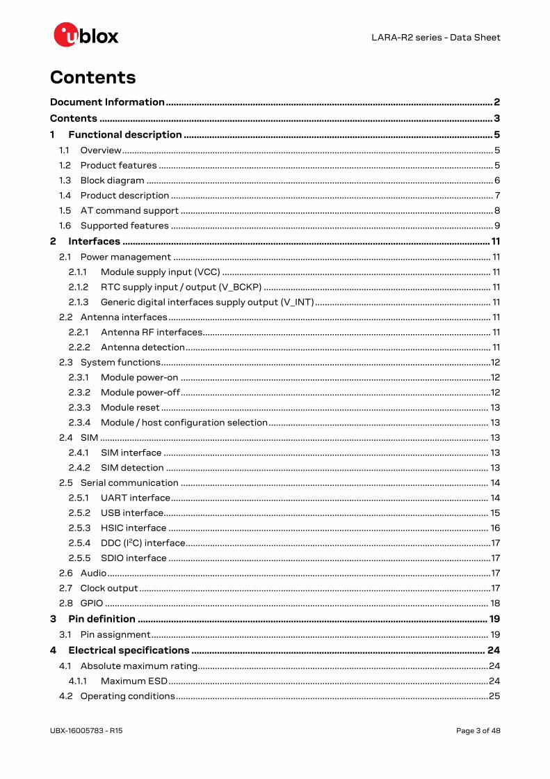
1.2 Product features
Model Region Radio Access
Technology Positioning Interfaces Audio Features Grade
LT
E b
an
ds
1
UM
TS
ba
nd
s
GS
M b
an
ds
GN
SS
via
mo
de
m
As
sis
tNo
w S
oft
wa
re
Ce
llL
oc
ate
®
UA
RT
US
B 2
.0
HIS
C *
SD
IO *
DD
C (
I2C
)
GP
IOs
An
alo
g a
ud
io
Dig
ita
l au
dio
Ne
two
rk in
dic
ati
on
Vo
LT
E
An
ten
na
su
pe
rvis
or
Ja
mm
ing
de
tec
tio
n
Em
be
dd
ed
TC
P/U
DP
sta
ck
Em
be
dd
ed
HT
TP
,FT
P,T
SL
1.2
FW
up
da
te v
ia s
eri
al
FO
TA
cli
en
t
Rx
Div
ers
ity
Du
al s
tac
k I
Pv
4 /
IP
v6
Sta
nd
ard
Pro
fes
sio
na
l
Au
tom
oti
ve
LARA-R202 North
America
2,4
5,12
850
1900 ● ● ● 1 1 1 1 1 9 ● ● ● ● □ ● ● ● ● ● ● ●
LARA-R203 North
America 2,4,12 ● ● ● 1 1 1 1 1 9 ● ● ● ● □ ● ● ● ● ● ● ●
LARA-R204 North
America 4,13 □ □ □ 1 1 1 1 1 9 □ ● ● □ ● ● ● ● ● ● ●
LARA-R211 Europe 3,7,20 900
1800 ● 2 ● 2 ● 2 1 1 1 1 1 9 ● ● ● ● □ ● ● ● ● ● ● ●
LARA-R220 Japan 1,19 ● ● ● 1 1 1 1 1 9 □ ● ● □ ● ● ● ● ● ● ●
LARA-R280 APAC 3,8,28 2100 ● ● ● 1 1 1 1 1 9 ● ● ■ ● □ ● ● ● ● ● ● ●
●= Available in any firmware ■ = CSFB only □ = Available in future firmware * = HW ready
Table 1: LARA-R2 series main features summary
1 LTE band 12 is a superset that includes band 17: the LTE band 12 is supported along with Multi-Frequency Band Indicator (MFBI) feature 2 Not supported by LARA-R211-02B-00
LARA-R2 series - Data Sheet
UBX-16005783 - R15 Functional description Page 6 of 48
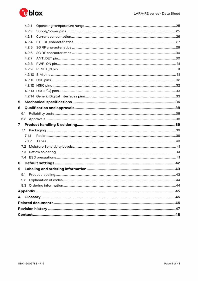
1.3 Block diagram
CellularBase-bandprocessor
Memory
Power Management Unit
26 MHz
32.768 kHz
ANT1
RF transceiver
ANT2
V_INT (I/O)
V_BCKP (RTC)
VCC (Supply)
SIM
USB
HSIC
Power On
External Reset
PAs
LNAs
Filters
FiltersDuplexer
Filters
PAs
LNAs
Filters
FiltersDuplexer
Filters
LNAs
Filters
Filters
LNAs
FiltersFilters
Switch
Switch
DDC(I2C)
SDIO
UART
ANT_DET
Host Select
GPIO
Digital audio (I2S)
Figure 1: LARA-R2 series block diagram
☞ The LARA-R2 series “02” and “62” product versions (i.e. the LARA-R202-02B, LARA-R203-02B,
LARA-R204-02B, LARA-R211-02B, LARA-R220-62B and LARA-R280-02B) do not support the
following interfaces, which can be left unconnected and should not be driven by external devices:
HSIC interface
SDIO interface
HOST_SELECT pin
LARA-R2 series - Data Sheet
UBX-16005783 - R15 Functional description Page 7 of 48
1.4 Product description
LARA-R2 series modules provide LTE Cat 1 technology, some variants with 2G or 3G multi-mode
fallback.
LARA-R202 is designed mainly for operation in America (on AT&T LTE and 3G network)
LARA-R203 is designed mainly for operation in America (on AT&T and T-Mobile LTE networks)
LARA-R204 is designed mainly for operation in America (on Verizon LTE network)
LARA-R211 is designed mainly for operation in Europe, Asia and other countries on LTE and 2G
networks
LARA-R220 is designed mainly for operation in Japan (on NTT DoCoMo LTE network)
LARA-R280 is designed mainly for operation in Asia, Oceania and other countries on LTE and 3G
networks
4G LTE 3G UMTS/HSDPA/HSUPA 2G GSM/GPRS/EDGE
3GPP Release 9
Long Term Evolution (LTE)
Evolved Univ. Terrestrial Radio Access
(E-UTRA)
Frequency Division Duplex (FDD)
DL Rx diversity
3GPP Release 9
High Speed Packet Access (HSPA)
UMTS Terrestrial Radio Access
(UTRA)
Frequency Division Duplex (FDD)
DL Rx Diversity
3GPP Release 9
Enhanced Data rate GSM Evolution (EDGE)
GSM EGPRS Radio Access (GERA)
Time Division Multiple Access (TDMA)
DL Advanced Rx Performance Phase 1
Band support3:
LARA-R202:
Band 12 (700 MHz) 4
Band 5 (850 MHz)
Band 4 (1700 MHz)
Band 2 (1900 MHz)
Band support:
LARA-R202:
Band 5 (850 MHz)
Band 2 (1900 MHz)
Band support:
LARA-R203:
Band 12 (700 MHz) 4
Band 4 (1700 MHz)
Band 2 (1900 MHz)
LARA-R204:
Band 13 (700 MHz)
Band 4 (1700 MHz)
LARA-R211:
Band 20 (800 MHz)
Band 3 (1800 MHz)
Band 7 (2600 MHz)
LARA-R211:
E-GSM 900 MHz
DCS 1800 MHz
LARA-R220:
Band 19 (850 MHz)
Band 1 (2100 MHz)
LARA-R280:
Band 28 (700 MHz)
Band 8 (900 MHz)
Band 3 (1800 MHz)
LARA-R280:
Band 1 (2100 MHz)
LTE Power Class
Power Class 3 (23 dBm)
UMTS/HSDPA/HSUPA Power Class
Class 3 (24 dBm)
GSM/GPRS (GMSK) Power Class
Power Class 4 (33 dBm) for E-GSM band
Power Class 1 (30 dBm) for DCS band
EDGE (8-PSK) Power Class
Power Class E2 (27 dBm) for E-GSM band
Power Class E2 (26 dBm) for DCS band
3 LARA-R2 series modules support all E-UTRA channel bandwidths for each operating band according to 3GPP TS 36.521-1 [11] 4 LTE band 12 is a superset that includes band 17: the LTE band 12 is supported along with Multi-Frequency Band Indicator
(MFBI) feature
LARA-R2 series - Data Sheet
UBX-16005783 - R15 Functional description Page 8 of 48
4G LTE 3G UMTS/HSDPA/HSUPA 2G GSM/GPRS/EDGE
Data rate
LTE category 1:
up to 10.3 Mbit/s DL,
up to 5.2 Mbit/s UL
Data rate
HSDPA category 8:
up to 7.2 Mbit/s DL
HSUPA category 6:
up to 5.76 Mbit/s UL
Data rate5
GPRS multi-slot class 336, CS1-CS4,
up to 107 kbit/s DL, up to 85.6 kbit/s UL
EDGE multi-slot class 336, MCS1-MCS9,
up to 296 kbit/s DL, up to 236.8 kbit/s UL
Table 2: LARA-R2 series LTE, 3G and 2G characteristics
LARA-R2 modules provide Voice over LTE (VoLTE)7 as well as Circuit-Switched-Fall-Back (CSFB) 8
audio capability.
1.5 AT command support
The LARA-R2 series modules support AT commands according to 3GPP standards TS 27.007 [7],
TS 27.005 [8] and the u-blox AT command extension.
☞ For the complete list of all supported AT commands and their syntax, see the u-blox AT
Commands Manual [1].
RIL (Radio Interface Layer) software for Android and Embedded Windows is available for LARA-R2
series modules free of charge; see the Android RIL Production delivery [3] application note for the
supported software deliveries and more information.
5 GPRS/EDGE multi-slot class determines the number of timeslots available for upload and download and thus the speed at
which data can be transmitted and received, with higher classes typically allowing faster data transfer rates. 6 GPRS/EDGE multi-slot class 33 implies a maximum of 5 slots in DL (reception) and 4 slots in UL (transmission) with 6 slots in
total. 7 Not supported by LARA-R204 and LARA-R280 modules “02” product version, LARA-R220 modules “62” product version. 8 Not supported by LARA-R203, LARA-R204 and LARA-R220 modules.
LARA-R2 series - Data Sheet
UBX-16005783 - R15 Functional description Page 9 of 48
1.6 Supported features
Table 3 lists some of the main features supported by LARA-R2 modules. For more details, see
LARA-R2 series System Integration Manual [2] and u-blox AT Commands Manual [1].
Feature Description
Network Indication GPIO configured to indicate the network status: registered home network, registered roaming,
voice or data call enabled, no service. The feature can be enabled through the +UGPIOC AT
command.
Antenna Detection The ANT_DET pin provides antenna presence detection capability, evaluating the resistance from
ANT1 and ANT2 pins to GND by means of an external antenna detection circuit implemented on
the application board.
The antenna detection feature can be enabled through the +UANTR AT command.
Jamming detection 9 Detects “artificial” interference that obscures the operator’s carriers entitled to give access to the
radio service and reports the start and stop of such conditions to the application processor that
can react accordingly.
Embedded TCP and UDP
stack
Embedded TCP/IP and UDP/IP stack including direct link mode for TCP and UDP sockets.
Sockets can be set in Direct Link mode to establish a transparent end to end communication with
an already connected TCP or UDP socket via serial interface.
FTP, FTPS File Transfer Protocol as well as Secure File Transfer Protocol (SSL encryption of FTP control
channel) functionalities are supported by means of AT commands.
HTTP, HTTPS Hyper-Text Transfer Protocol as well as Secure Hyper-Text Transfer Protocol (SSL encryption)
functionalities are supported via AT commands. HEAD, GET, POST, DELETE and PUT operations
are available.
Embedded TLS 1.2 With the support of X.509 certificates, Embedded TLS 1.2 provides server and client
authentication, data encryption, data signature and enables TCP/IP applications like HTTPS and
FTPS to communicate over a secured and trusted connection.
The feature can be configured and enabled by +USECMNG and +USECPRF AT commands.
DNS Support for DNS functionality.
IPv4/Ipv6 dual-stack Capability to move between Ipv4 and dual stack network infrastructures. Ipv4 and Ipv6 addresses
can be used.
PPP Ipv4/Ipv6 packets relaying through the cellular protocol stack performed on a Point-to-Point
Protocol connection established with the external application via a serial interface (UART, MUX, or
CDC-ACM). Transitions between Online command mode (OLCM) and PPP mode are supported.
BIP Bearer Independent Protocol for Over-the-Air SIM provisioning. The data transfer to/from the SIM
uses either an already active PDP context or a new PDP context established with the APN provided
by the SIM card.
Multiple PDP contexts Up to 8 PDP contexts can be activated, and multi secondary PDP contexts be associated to a
primary PDP context.
VoLTE 10 and CSFB 11
audio capability
Voice over LTE (VoLTE) feature allows voice service over LTE bearer, via embedded IP Multimedia
Subsystem (IMS).
Circuit Switched Fall-Back (CSFB) feature allows voice service over circuit switched infrastructure
(3G or 2G).
Firmware update Over AT
commands (FOAT)
Firmware module update over AT command interfaces.
The feature can be enabled and configured through the +UFWUPD AT command.
Firmware update Over
The Air (FOTA)
Embedded FOTA client to enable the Firmware module update over the cellular air interface.
The feature can be enabled and configured through the +UFWINSTALL AT command.
LTE / 3G Rx Diversity Improved cellular link quality and reliability on all operating bands, by means of 2 receiving antenna
inputs.
GNSS via modem12 Full access to u-blox positioning chips and modules is available through a dedicated DDC (I2C)
interface. This means that from any host processor, a single serial port can control the cellular
9 Not supported by “02” and “62” product versions. 10 Not supported by LARA-R204 and LARA-R280 modules “02” product version, LARA-R220 modules “62” product version. 11 Not supported by LARA-R203, LARA-R204 and LARA-R220 modules. 12 Not supported by LARA-R204-02B, LARA-R211-02B-00 product versions.
LARA-R2 series - Data Sheet
UBX-16005783 - R15 Functional description Page 10 of 48
Feature Description
module and the u-blox M8 positioning chip or module. For more details, see the GNSS
Implementation Application Note [4].
Embedded AssistNow
Software12
Embedded AssistNow Online and AssistNow Offline clients are available to provide better GNSS
performance and faster Time-to-First-Fix. An AT command can enable / disable the clients.
CellLocate®12 Enables the estimation of device position based on the parameters of the mobile network cells
visible to the specific device based on the CellLocate® database:
Normal scan: only the parameters of the visible home network cells are sent CellLocate® is available via a set of AT commands for CellLocate® service configuration and
position request.
Hybrid Positioning12 The current module position is provided by a u-blox positioning chip or module or the estimated
position from CellLocate® depending on which method provides the best and fastest solution
according to the user configuration.
Hybrid positioning is available via a set of AT commands that allow the configuration and the
position request.
Wi-Fi via modem13 Full access to Wi-Fi modules is available through a dedicated SDIO interface. This means that
from any host processor a single serial port can control the cellular module and the short range
communication module.
DTMF decoder14 During a voice call, the Dual-Tone Multi-Frequency detector analyses the RX speech (coming from
remote party). The detected DTMF symbols can be output via the related URC.
The feature can be enabled and configured through the +UDTMFD AT command.
In-Band Modem13 In-Band modem solution for eCall and ERA-GLONASS emergency call applications over cellular
networks implemented according to the 3GPP TS 26.267 specification [10].
When activated, the in-vehicle eCall / ERA-GLONASS system (IVS) creates an emergency call
carrying both voice and data (including vehicle position data) directly to the nearest Public Safety
Answering Point (PSAP) to determine whether rescue services should be dispatched to the known
position.
Smart Temperature
Supervisor
Constant monitoring of the module board temperature:
Warning notification when the temperature approaches an upper or lower predefined
threshold
Shutdown notified and forced when the temperature value is outside the specified range
(shutdown suspended in case of an emergency call in progress)
The Smart Temperature Supervisor feature can be enabled and configured through the +USTS AT
command.
☞ The sensor measures the board temperature, which can differ from ambient temperature.
Power saving The power saving configuration is disabled by default, but it can be enabled and configured using
the +UPSV AT command. When the power saving is enabled, the module automatically enters the
low power idle-mode whenever possible, reducing current consumption.
During idle-mode, the module processor core runs with the RTC 32 kHz reference clock, which is
generated by the internal 32 kHz oscillator.
Fast Dormancy The Fast Dormancy feature, defined in 3GPP Rel.8, allows reduction of current consumption and
network utilization during periods of data inactivity. It can be activated and configured by +UFDAC
and +UDCONF=61 AT commands.
LTE cDRX Both the Long DRX Cycle and the Short DRX cycle are supported for LTE Connected Discontinuous
Reception, allowing reduction of current consumption and LTE network utilization during periods
of data inactivity.
Power Saving Mode (PSM)
as specified in 3GPP
Release 12 13
The Power Saving Mode (PSM) feature, defined in 3GPP Rel.12, allows further reduction of the
module current consumption by decreasing the signaling load between the module and the
network on non-access stratum level during periods of data inactivity. It can be activated and
configured by dedicated AT commands.
Table 3: Some of the main features supported by LARA-R2 series modules
☞ u-blox is extremely mindful of user privacy. When a position is sent to the CellLocate® server, u-blox
is unable to track the SIM used or the specific device.
13 Not supported by “02” and “62” product versions. 14 Not supported by LARA-R204 module “02” product version, LARA-R220 modules “62” product version.
LARA-R2 series - Data Sheet
UBX-16005783 - R15 Interfaces Page 11 of 48
2 Interfaces
2.1 Power management
2.1.1 Module supply input (VCC)
LARA-R2 series modules must be supplied through the three VCC pins by a DC power supply. Voltage
must be stable, because during operation the current drawn from VCC can vary by some order of
magnitude, especially due to the surging consumption profile of the GSM system (described in the
LARA-R2 series System Integration Manual [2]). It is important that the system power supply circuit
is able to support peak power.
LARA-R211 modules provide separate supply inputs over the three VCC pins:
VCC pins #52 and #53 represent the supply input for the internal RF power amplifier, demanding
most of the total current drawn of the module when RF transmission is enabled during a
voice/data call
VCC pin #51 represents the supply input for the internal baseband Power Management Unit and
the internal transceiver, demanding a minor part of the total current drawn of the module when
RF transmission is enabled during a voice/data call
2.1.2 RTC supply input / output (V_BCKP)
When VCC voltage is within the valid operating range, the internal Power Management Unit (PMU)
supplies the Real Time Clock (RTC) and the same supply voltage is available on the V_BCKP pin. If the
VCC voltage is under the minimum operating limit (e.g. during not powered mode), the V_BCKP pin
can externally supply the RTC.
2.1.3 Generic digital interfaces supply output (V_INT)
LARA-R2 series modules provide a 1.8 V supply rail output on the V_INT pin, which is internally
generated when the module is switched on. The same voltage domain is used internally to supply the
generic digital interfaces of the modules. The V_INT supply output can be used in place of an external
discrete regulator.
2.2 Antenna interfaces
2.2.1 Antenna RF interfaces
The modules have two RF pins with a characteristic impedance of 50 . The primary antenna pin
(ANT1) supports both Tx and Rx, providing the main antenna interface, while the secondary antenna
pin (ANT2) supports Rx only for the LTE / 3G Rx diversity configuration.
2.2.2 Antenna detection
The ANT_DET pin is an Analog to Digital Converter (ADC) input with a current source provided by
LARA-R2 modules to sense the antenna(s) presence (as an optional feature). It evaluates the
resistance from ANT1 and ANT2 pins to GND by means of an external antenna detection circuit
implemented on the application board. For more details, see the LARA-R2 series System Integration
Manual [2] and the u-blox AT Commands Manual [1].
LARA-R2 series - Data Sheet
UBX-16005783 - R15 Interfaces Page 12 of 48
2.3 System functions
2.3.1 Module power-on
LARA-R2 series modules can be switched on in one of the following ways:
Rising edge on the VCC input to a valid voltage for module supply, i.e. applying module supply: the
modules switch on if the VCC supply is applied, starting from a voltage value of less than 2.1 V,
with a rise time from 2.3 V to 2.8 V of less than 4 ms, reaching a proper nominal voltage value
within VCC operating range.
Alternately, for example if the fast rise time on VCC rising edge cannot be guaranteed by the
application, the LARA-R2 series module can be switched on from not-powered mode as follows:
RESET_N input pin is held low by the external application during the VCC rising edge, so that the
module will switch on when the external application releases the RESET_N input pin from the low
logic level, after the VCC supply voltage stabilizes at its proper nominal value within the operating
range
PWR_ON input pin is held low by the external application during the VCC rising edge, so that the
module will switch on when the external application releases the PWR_ON input pin from the low
logic level, after the VCC supply voltage stabilizes at its proper nominal value within the operating
range
When the LARA-R2 series modules are in the power-off mode (i.e. properly switched off as described
in section 2.3.2, with valid VCC module supply applied), they can be switched on as following:
Low pulse on the PWR_ON pin, which is normally set high by an internal pull-up, for a valid time
period (see section 4.2.8). The PWR_ON line should be driven by open drain, open collector or
contact switch.
Rising edge on the RESET_N pin, i.e. releasing the pin from the low level, normally set high by an
internal pull-up. The RESET_N line should be driven by open drain, open collector or contact switch.
RTC alarm, i.e. pre-programmed scheduled time by AT+CALA command.
2.3.2 Module power-off
LARA-R2 series can be properly switched off, saving current parameter settings in the module’s non-
volatile memory and performing a proper network detach, by:
AT+CPWROFF command (see the u-blox AT Commands Manual [1]).
Low pulse on the PWR_ON pin, which is normally set high by an internal pull-up, for a valid time
period (see section 4.2.8). The PWR_ON line should be driven by open drain, open collector or
contact switch.
An abrupt under-voltage shutdown occurs on LARA-R2 series modules when the VCC supply is
removed. If this occurs, it is not possible to store the current parameter settings in the module’s non-
volatile memory or to perform the proper network detach.
An abrupt shutdown occurs on LARA-R2 series modules when a low level is applied on the RESET_N
pin, which is normally set high by an internal pull-up. If this occurs, it is not possible to store the
current parameter settings in the module’s non-volatile memory and to perform the proper network
detach.
An over-temperature or an under-temperature shutdown occurs on LARA-R2 modules when the
temperature measured within the cellular module reaches the dangerous area, if the optional Smart
Temperature Supervisor feature is enabled and configured by the dedicated AT command. For more
details, see the LARA-R2 series System Integration Manual [2] and the u-blox AT Commands
Manual [1], +USTS AT command.
LARA-R2 series - Data Sheet
UBX-16005783 - R15 Interfaces Page 13 of 48
2.3.3 Module reset
LARA-R2 series modules can be reset (rebooted) by:
AT+CFUN command (see the u-blox AT Commands Manual [1]). This causes an “internal” or
“software” reset of the module. The current parameter settings are saved in the module’s non-
volatile memory and a proper network detach is performed.
An abrupt “external” or “hardware” reset occurs when a low level is applied to the RESET_N pin, which
is normally set high by an internal pull-up, for a valid time period (see the section 4.2.9). This causes
an “external” or “hardware” reset of the entire module, including the integrated power management
unit, except for the RTC internal block: the V_INT generic digital interfaces supply is switched off and
all the digital pins are tri-stated, but the V_BCKP supply and the RTC block are enabled. The current
parameter settings are not saved in the module’s non-volatile memory and a proper network detach
is not performed. The RESET_N line should be driven by open drain, open collector or contact switch.
2.3.4 Module / host configuration selection
☞ The functionality of the HOST_SELECT pin is not supported by “02” and “62” product versions.
The modules include one pin (HOST_SELECT) to select the module / host application processor
configuration: the pin is available to select, enable, connect, disconnect and subsequently reconnect
the HSIC interface.
2.4 SIM
2.4.1 SIM interface
A SIM card interface is provided on the VSIM, SIM_IO, SIM_CLK, SIM_RST pins: the high-speed
SIM/ME interface is implemented as well as the automatic detection of the required SIM supporting
voltage.
Both 1.8 V and 3 V SIM types are supported (1.8 V and 3 V ME). Activation and deactivation with
automatic voltage switch from 1.8 V to 3 V is implemented, according to ISO-IEC 7816-3 specifications.
The SIM driver supports the PPS procedure for baud-rate selection, according to the values proposed
by the SIM card/chip.
2.4.2 SIM detection
LARA-R2 series modules provide the SIM detection function over the GPIO5 pin to sense the SIM card
physical presence (as an optional feature) when the pin of the module is properly connected to the
mechanical switch of the SIM car holder. For more details, see the LARA-R2 series System Integration
Manual [2].
LARA-R2 series - Data Sheet
UBX-16005783 - R15 Interfaces Page 14 of 48
2.5 Serial communication
LARA-R2 series modules provide the following serial communication interfaces:
UART interface: Universal Asynchronous Receiver/Transmitter serial interface available for the
communication with a host application processor (AT commands, data communication, FW
update by means of FOAT), for FW update by means of the u-blox EasyFlash tool and for
diagnostic.
USB interface: Universal Serial Bus 2.0 compliant interface available for the communication with
a host application processor (AT commands, data communication, FW update by means of the
FOAT feature), for FW update by means of the u-blox EasyFlash tool and for diagnostic.
HSIC interface: High-Speed Inter-Chip USB compliant interface available for the communication
with a host application processor (AT commands, data communication, FW update by means of
the FOAT feature), for FW update by means of the u-blox EasyFlash tool and for diagnostic.
DDC interface: I2C bus compatible interface available for the communication with u-blox GNSS
positioning chips/modules and with external I2C devices as an audio codec.
SDIO interface: Secure Digital Input Output interface available for the communication with
compatible u-blox short range radio communication Wi-Fi modules.
2.5.1 UART interface
LARA-R2 series modules include a 9-wire unbalanced Universal Asynchronous Receiver/Transmitter
serial interface (UART) for communication with an application host processor (AT commands, data
communication, FW update by means of the FOAT feature), for FW update by means of the u-blox
EasyFlash tool and for diagnostic.
UART features are:
Complete serial port with RS-232 functionality conforming to the ITU-T V.24
Recommendation [14], with CMOS compatible signal levels (0 V for low data bit or ON state and
1.8 V for high data bit or OFF state)
Data lines (RXD as output, TXD as input), hardware flow control lines (CTS as output, RTS as
input), modem status and control lines (DTR as input, DSR as output, DCD as output, RI as output)
are provided
Hardware flow control (default value), software flow control, or none flow control are supported
Power saving indication available on the hardware flow control output (CTS line): the line is driven
to the OFF state when the module is not prepared to accept data by the UART interface
Power saving control over the RTS input or the DSR input can be enabled via AT+UPSV command
(for more details, see u-blox AT Commands Manual [1] and LARA-R2 series System Integration
Manual [2])
The following baud rates are supported: 9600, 19200, 38400, 57600, 115200 (default baud rate
when autobauding is disabled), 230400, 460800, 921600, 3000000, 3250000, 6000000 and
6500000 bit/s
One-shot autobauding is supported and it is enabled by default: automatic baud rate detection is
performed only once, at module start up. After the detection, the module works at the fixed baud
rate (the detected one) and the baud rate can only be changed via AT command (see the u-blox AT
Commands Manual [1], +IPR).
The following frame formats are supported: 8N2, 8N1 (default format when automatic frame
recognition is disabled), 8E1, 8O1, 7E1 and 7O1.
One-shot automatic frame recognition is supported and it is enabled by default in conjunction with
automatic baud rate detection (autobauding): the detection is performed only once, at module
start up. After the detection, the module works at the detected frame format and it can only be
changed via AT command (see u-blox AT Commands Manual [1], +ICF).
LARA-R2 series - Data Sheet
UBX-16005783 - R15 Interfaces Page 15 of 48
UART serial interface can be conveniently configured through AT commands: see the u-blox AT
Commands Manual [1] (+IPR, +ICF, +IFC, &K, \Q, +UPSV AT commands) and LARA-R2 series System
Integration Manual [2].
2.5.1.1 Multiplexer protocol
LARA-R2 series modules include multiplexer functionality as per 3GPP TS 27.010 [9] on the UART
physical link.
This is a data link protocol which uses HDLC-like framing and operates between the module (DCE) and
the application processor (DTE), allowing a number of simultaneous sessions over the physical link
(UART): the user can concurrently use AT interface on one MUX channel and data communication on
another MUX channel.
The following virtual channels are available (for more details, see the Mux Implementation Application
Note [5]):
Channel 0: Multiplexer control
Channel 1 – 5: AT commands / data connection
Channel 6: GNSS data tunneling
☞ GNSS data tunneling is not supported by LARA-R204-02B-00 and LARA-R211-02B-00 product
versions.
2.5.2 USB interface
LARA-R2 series modules include a USB High-Speed 2.0 compliant interface with a maximum
480 Mbit/s data rate according to the Universal Serial Bus Specification Revision 2.0 [15]. The module
itself acts as a USB device and can be connected to any compatible USB host.
The USB interface is available for communication with a host application processor (AT commands,
data communication, FW update by means of the FOAT feature), for FW update by means of the
u-blox EasyFlash tool and for diagnostics.
The USB_D+ / USB_D- lines carry the USB data and signaling. The USB interface is automatically
enabled by an external valid USB VBUS supply voltage (5.0 V typical) applied on the VUSB_DET pin.
The USB interface of LARA-R2 series modules makes several USB functions available with various
capabilities and purposes, such as:
CDC-ACM for AT commands and data communication
CDC-ACM for GNSS tunneling
CDC-ACM for SAP (SIM Access Profile)
CDC-ACM for Diagnostic log
CDC-NCM for Ethernet-over-USB
☞ CDC-ACM for GNSS tunneling is not supported by LARA-R204-02B and LARA-R211-02B product
versions.
☞ CDC-ACM for SAP and CDC-NCM for Ethernet-over-USB are not supported by “02” and “62”
versions.
LARA-R2 series - Data Sheet
UBX-16005783 - R15 Interfaces Page 16 of 48
The USB interface provides the following set of USB functions:
6 CDC-ACM modem COM ports enumerated as follows:
o USB1: AT and data
o USB2: AT and data
o USB3: AT and data
o USB4: GNSS tunneling
o USB5: SAP (SIM Access Profile)
o USB6: diagnostic log
The user can concurrently use the AT command interface on one CDC, and Packet-Switched / Circuit-
Switched Data communication on another CDC.
For more details regarding USB capabilities, see the LARA-R2 series System Integration Manual [2].
USB drivers are available for the following Windows and Windows Embedded operating system
platforms:
Windows 7
Windows 8
Windows 8.1
Windows 10
Windows Embedded CE 6.0
Windows Embedded Compact 7
Windows Embedded Compact 2013
Windows 10 IoT
LARA-R2 series modules are compatible with the standard Linux/Android USB kernel drivers.
2.5.3 HSIC interface
☞ The HSIC interface is not supported by “02” and “62” product versions except for diagnostic
purposes.
LARA-R2 series modules include a USB High-Speed Inter-Chip compliant interface with a maximum
480 Mbit/s data rate as per the High-Speed Inter-Chip USB Electrical Specification Version 1.0 [16]
and USB Specification Revision 2.0 [15]. The module itself acts as a device and can be connected to
any compatible host.
The HSIC interface is available for communication with a host application processor (AT commands,
data communication, FW update by means of the FOAT feature), for FW update by means of the
u-blox EasyFlash tool and for diagnostics.
The HSIC interface consists of a bi-directional DDR data line (HSIC_DATA) for transmitting and
receiving data synchronously with the bi-directional strobe line (HSIC_STRB).
The modules also include the HOST_SELECT pin to select the module / host application processor
configuration: the pin is available to select, enable, connect, disconnect and subsequently reconnect
the HSIC interface.
LARA-R2 series - Data Sheet
UBX-16005783 - R15 Interfaces Page 17 of 48
2.5.4 DDC (I2C) interface
☞ Communication with u-blox GNSS receivers over DDC (I2C) is not supported by LARA-R204-02B
and LARA-R211-02B product versions.
LARA-R2 series modules include an I2C-bus compatible DDC interface (SDA, SCL) available to
communicate with a u-blox GNSS receiver and with external I2C devices as an audio codec: the LARA-
R2 module acts as an I2C master which can communicate with I2C slaves in accordance with the I2C
bus specifications [17].
For more details regarding the DDC (I2C) interface usage and the integration with a u-blox GNSS
receiver, see the LARA-R2 series System Integration Manual [2], the GNSS Implementation
Application Note [4], and the I2C and GNSS AT commands description in the u-blox AT Commands
Manual [1].
2.5.5 SDIO interface
☞ The SDIO interface is not supported by the “02” and “62” module product versions.
LARA-R2 series modules include a 4-bit Secure Digital Input Output interface (SDIO_D0, SDIO_D1,
SDIO_D2, SDIO_D3, SDIO_CLK, SDIO_CMD) designed to communicate with external compatible
u-blox short range radio communication Wi-Fi modules.
2.6 Audio
☞ Audio is not supported by LARA-R204-02B and LARA-R220-62B module product versions.
LARA-R2 series modules support Voice over LTE (VoLTE) as well as Circuit-Switched Fall-Back (CSFB)
from LTE to 3G or 2G radio bearer for providing audio services.
LARA-R2 series modules include a 4-wire I2S digital audio interface (I2S_TXD, I2S_RXD, I2S_CLK,
I2S_WA) that can be configured by AT command in PCM mode (short synchronization signal) or in
normal I2S mode (long synchronization signal) to transfer digital audio data to/from an external device
as an audio codec.
For more details regarding internal audio processing system capabilities, I2S digital audio interface
possible configurations, usage and guideline for the integration with an external digital audio device
as an audio codec, see the LARA-R2 series System Integration Manual [2] and the audio sections in
the u-blox AT Commands Manual [1].
2.7 Clock output
LARA-R2 series modules provide master digital clock output functionality on the GPIO6 pin, which can
be configured to provide a 13 MHz or 26 MHz square wave. This is mainly designed to feed the master
clock input of an external audio codec, as the clock output can be configured in “Audio dependent”
mode (generating the square wave only when the audio path is active), or in “Continuous” mode.
For more details, see the u-blox AT Commands Manual [1], +UMCLK AT command.
LARA-R2 series - Data Sheet
UBX-16005783 - R15 Interfaces Page 18 of 48
2.8 GPIO
LARA-R2 series modules include 9 pins (GPIO1-GPIO5, I2S_TXD, I2S_RXD, I2S_CLK, I2S_WA) that can
be configured as general purpose input/output or to provide custom functions as summarized in Table
4 (for further details, see the LARA-R2 series System Integration Manual [2] and the GPIO section in
the u-blox AT Commands Manual [1]).
Function Description Default GPIO Configurable GPIOs
Network status
indication
Network status: registered home network,
registered roaming, data transmission, no service
-- GPIO1-GPIO4
GNSS supply enable 15 Enable/disable the supply of u-blox GNSS receiver
connected to the cellular module
GPIO2 GPIO1-GPIO4
GNSS data ready 15 Sense when u-blox GNSS receiver connected to the
module is ready for sending data by the DDC (I2C)
GPIO3 GPIO3
GNSS RTC sharing 16 RTC synchronization signal to the u-blox GNSS
receiver connected to the cellular module
-- GPIO4
SIM card detection External SIM card physical presence detection GPIO5 GPIO5
SIM card hot
insertion/removal
Enable / disable SIM interface upon detection of
external SIM card physical insertion / removal
-- GPIO5
I2S digital audio interface I2S digital audio interface I2S_RXD, I2S_TXD,
I2S_CLK, I2S_WA
I2S_RXD, I2S_TXD,
I2S_CLK, I2S_WA
Wi-Fi control 16 Control of an external Wi-Fi chip or module -- --
General purpose input Input to sense high or low digital level -- All
General purpose output Output to set the high or the low digital level GPIO4 All
Pin disabled Tri-state with an internal active pull-down enabled GPIO1 All
Table 4: GPIO custom functions configuration
15 Not supported by LARA-R204-02B and LARA-R211-02B-00 product versions: GPIO2 and GPIO3 pins are by default disabled 16 Not supported by “02” and “62” product versions
LARA-R2 series - Data Sheet
UBX-16005783 - R15 Pin definition Page 19 of 48
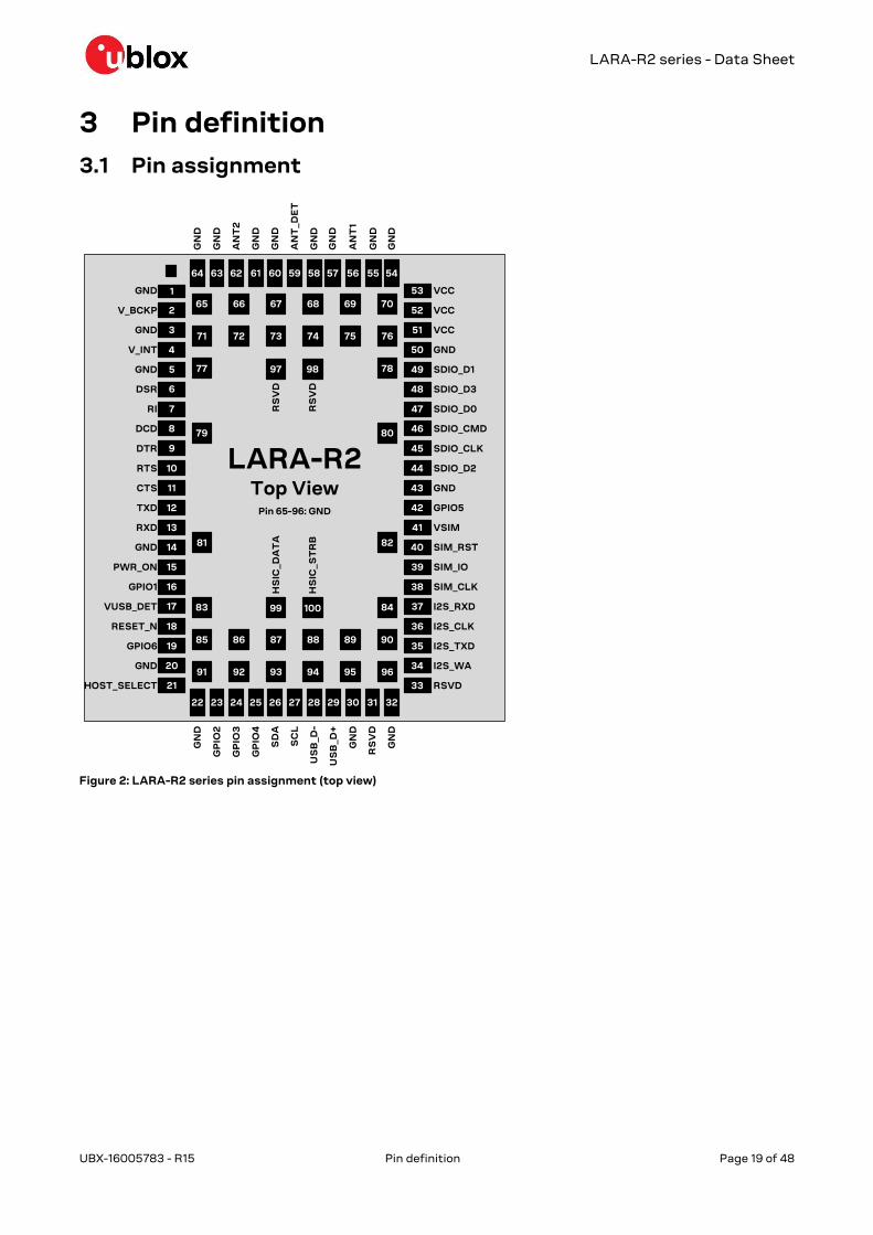
3 Pin definition
3.1 Pin assignment
64 63 61 60 58 57 55 54
22
50
65 66 67 68 69 70
71 72 73 74 75 76
77 78
79 80
81 82
83 84
85 86 87 88 89 90
91 92 93 94 95 96
CTS
RTS
DCD
RI
V_INT
V_BCKP
GND
GPIO6
RESET_N
GPIO1
PWR_ON
RXD
TXD
11
10
8
7
5
4
2
1
21
19
18
16
15
13
12
3
20
17
14
9
6
23 25 26 28 29 31 3224 27 30
43
44
46
47
49
52
53
33
35
36
38
39
41
42
51
48
45
40
37
34
5962 56
GND
GND
DSR
DTR
GND
VUSB_DET
GND
US
B_D
-
US
B_D
+
RS
VD
GN
D
GP
IO2
GP
IO3
SD
A
SC
L
GP
IO4
GN
D
GN
D
GND
GND
VCC
VCC
RSVD
I2S_TXD
I2S_CLK
SIM_CLK
SIM_IO
VSIM
GPIO5
VCC
SIM_RST
I2S_RXD
I2S_WA
GN
D
GN
D
GN
D
GN
D
GN
D
GN
D
GN
D
GN
D
AN
T_D
ET
AN
T2
AN
T1
LARA-R2Top View
Pin 65-96: GND
99 100
97 98
RS
VD
RS
VD
HS
IC_S
TR
B
HS
IC_D
AT
A
HOST_SELECT
SDIO_D2
SDIO_CMD
SDIO_D0
SDIO_D1
SDIO_D3
SDIO_CLK
Figure 2: LARA-R2 series pin assignment (top view)
LARA-R2 series - Data Sheet
UBX-16005783 - R15 Pin definition Page 20 of 48
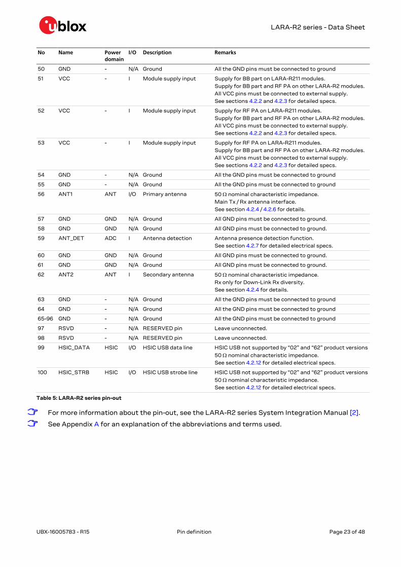
No Name Power
domain
I/O Description Remarks
1 GND - N/A Ground All the GND pins must be connected to ground
2 V_BCKP - I/O Real Time Clock supply
input/output
V_BCKP = 1.8 V (typical) generated by the module to supply
the RTC when VCC voltage is within valid operating range.
See section 4.2.2 for detailed electrical specs.
3 GND - N/A Ground All the GND pins must be connected to ground
4 V_INT - O Generic Digital Interfaces
supply output
V_INT = 1.8 V (typical) generated by the module when it is
switched-on and with the RESET_N pin is not forced low.
See section 4.2.2 for detailed electrical specs.
5 GND - N/A Ground All the GND pins must be connected to ground
6 DSR GDI O UART data set ready Circuit 107 (DSR) in ITU-T V.24.
Output driver class A. PU/PD class a.
Value at internal reset: T/PU.
See section 4.2.14 for detailed electrical specs.
7 RI GDI O UART ring indicator Circuit 125 (RI) in ITU-T V.24.
Output driver class A. PU/PD class a.
Value at internal reset: T/PD.
See section 4.2.14 for detailed electrical specs.
8 DCD GDI O UART data carrier detect Circuit 109 (DCD) in ITU-T V.24.
Output driver class A. PU/PD class a.
Value at internal reset: T/PD.
See section 4.2.14 for detailed electrical specs.
9 DTR GDI I UART data terminal ready Circuit 108/2 (DTR) in ITU-T V. 24.
Internal active pull-up to V_INT enabled. PU/PD class a.
Value at internal reset: T/PU.
See section 4.2.14 for detailed electrical specs.
10 RTS GDI I UART ready to send Circuit 105 (RTS) in ITU-T V.24.
Internal active pull-up to V_INT enabled. PU/PD class a.
Value at internal reset: T/PU.
See section 4.2.14 for detailed electrical specs.
11 CTS GDI O UART clear to send Circuit 106 (CTS) in ITU-T V.24.
Output driver class A. PU/PD class a.
Value at internal reset: T/PU.
See section 4.2.14 for detailed electrical specs.
12 TXD GDI I UART data input Circuit 103 (TxD) in ITU-T V.24.
Internal active pull-up to V_INT enabled. PU/PD class a.
Value at internal reset: T/PD.
See section 4.2.14 for detailed electrical specs.
13 RXD GDI O UART data output Circuit 104 (RxD) in ITU-T V.24.
Output driver class A. PU/PD class a.
Value at internal reset: T/PU.
See section 4.2.14 for detailed electrical specs.
14 GND - N/A Ground All the GND pins must be connected to ground
15 PWR_ON POS I Power-on input Internal 10 k pull-up resistor to V_BCKP.
See section 4.2.8 for detailed electrical specs.
16 GPIO1 GDI I/O GPIO GPIO configurable as described in section 2.8.
Output driver class A. PU/PD class b.
Value at internal reset: T/PD.
See section 4.2.14 for detailed electrical specs.
17 VUSB_DET VBUS I VBUS USB detect input VBUS (5 V typical) USB supply generated by the host must
be connected to this input pin to enable the USB interface.
See section 4.2.11 for detailed electrical specs.
18 RESET_N ERS I External reset input Internal 10 k pull-up resistor to V_BCKP.
See section 4.2.9 for detailed electrical specs.
LARA-R2 series - Data Sheet
UBX-16005783 - R15 Pin definition Page 21 of 48
No Name Power
domain
I/O Description Remarks
19 GPIO6 GDI O Clock output Configurable clock output (see section 2.7).
Output driver class A. PU/PD class a.
Value at internal reset: T/PD.
See section 4.2.14 for detailed electrical specs.
20 GND - N/A Ground All the GND pins must be connected to ground
21 HOST_SELECT GDI I/O Selection of module / host
processor configuration
Not supported by “02” and “62” product versions.
Output driver class A. PU/PD class a.
Value at internal reset: T/PD.
See section 4.2.14 for detailed electrical specs.
22 GND - N/A Ground All the GND pins must be connected to ground
23 GPIO2 GDI I/O GPIO GPIO configurable as described in section 2.8.
Output driver class A. PU/PD class a.
Value at internal reset: T/PD.
See section 4.2.14 for detailed electrical specs.
24 GPIO3 GDI I/O GPIO GPIO configurable as described in section 2.8.
Output driver class A. PU/PD class a.
Value at internal reset: T/PD.
See section 4.2.14 for detailed electrical specs.
25 GPIO4 GDI I/O GPIO GPIO configurable as described in section 2.8.
Output driver class A. PU/PD class a.
Value at internal reset: T/PD.
See section 4.2.14 for detailed electrical specs.
26 SDA DDC I/O I2C bus data line Fixed open drain.
See section 4.2.13 for detailed electrical specs.
27 SCL DDC O I2C bus clock line Fixed open drain.
See section 4.2.13 for detailed electrical specs.
28 USB_D- USB I/O USB Data Line D- 90 nominal differential characteristic impedance.
Pull-up, pull-down and series resistors as required by the
USB 2.0 specifications [15] are part of the USB pin driver,
and need not be provided externally.
See section 4.2.11 for detailed electrical specs.
29 USB_D+ USB I/O USB Data Line D+ 90 nominal differential characteristic impedance.
Pull-up, pull-down and series resistors as required by the
USB 2.0 specifications [15] are part of the USB pin driver,
and need not be provided externally.
See section 4.2.11 for detailed electrical specs.
30 GND - N/A Ground All the GND pins must be connected to ground
31 RSVD - N/A RESERVED pin Leave unconnected.
32 GND - N/A Ground All the GND pins must be connected to ground
33 RSVD - N/A RESERVED pin This pin has special function: it must be connected to GND
to allow module to work properly.
LARA-R2 series - Data Sheet
UBX-16005783 - R15 Pin definition Page 22 of 48
No Name Power
domain
I/O Description Remarks
34 I2S_WA GDI I/O /
I/O
I2S word alignment /
GPIO
Configurable as I2S word alignment, or as GPIO (see 2.8).
I2S not supported by LARA-R204-02B and LARA-R220-62B.
Output driver class A. PU/PD class a.
Value at internal reset: T/PD.
See section 4.2.14 for detailed electrical specs.
35 I2S_TXD GDI O /
I/O
I2S transmit data /
GPIO
Configurable as I2S transmit data out, or as GPIO (see 2.8).
I2S not supported by LARA-R204-02B and LARA-R220-62B.
Output driver class A. PU/PD class a.
Value at internal reset: T/PD.
See section 4.2.14 for detailed electrical specs.
36 I2S_CLK GDI I/O /
I/O
I2S clock /
GPIO
Configurable as I2S clock, or as GPIO (see 2.8).
I2S not supported by LARA-R204-02B and LARA-R220-62B.
Output driver class A. PU/PD class a.
Value at internal reset: T/PD.
See section 4.2.14 for detailed electrical specs.
37 I2S_RXD GDI I /
I/O
I2S receive data /
GPIO
Configurable as I2S receive data input, or as GPIO (see 2.8).
I2S not supported by LARA-R204-02B and LARA-R220-62B.
Output driver class A. PU/PD class a.
Value at internal reset: T/PD.
See section 4.2.14 for detailed electrical specs.
38 SIM_CLK SIM O SIM clock See section 4.2.9 for detailed electrical specs.
39 SIM_IO SIM I/O SIM data Internal 4.7 k pull-up resistor to VSIM.
See section 4.2.9 for detailed electrical specs.
40 SIM_RST SIM O SIM reset See section 4.2.9 for detailed electrical specs.
41 VSIM - O SIM supply output VSIM = 1.80 V typical or 2.90 V typical generated by the
module according to the external SIM card/chip type.
See section 4.2.2 for detailed electrical specs.
42 GPIO5 GDI I/O GPIO Configurable for SIM card detection, or as GPIO (see 2.8).
Output driver class A. PU/PD class a.
Value at internal reset: T/PD.
See section 4.2.14 for detailed electrical specs.
43 GND - N/A Ground All the GND pins must be connected to ground
44 SDIO_D2 GDI I/O SDIO serial data [2] SDIO not supported by “02” and “62” product versions.
Output driver class A. PU/PD class a.
Value at internal reset: T/PD.
See section 4.2.14 for detailed electrical specs.
45 SDIO_CLK GDI O SDIO serial clock SDIO not supported by “02” and “62” product versions.
Output driver class A. PU/PD class a.
Value at internal reset: T/PD.
See section 4.2.14 for detailed electrical specs.
46 SDIO_CMD GDI I/O SDIO command SDIO not supported by “02” and “62” product versions.
Output driver class A. PU/PD class a.
Value at internal reset: T/PD.
See section 4.2.14 for detailed electrical specs.
47 SDIO_D0 GDI I/O SDIO serial data [0] SDIO not supported by “02” and “62” product versions.
Output driver class A. PU/PD class a.
Value at internal reset: T/PD.
See section 4.2.14 for detailed electrical specs.
48 SDIO_D3 GDI I/O SDIO serial data [3] SDIO not supported by “02” and “62” product versions.
Output driver class A. PU/PD class a.
Value at internal reset: T/PD.
See section 4.2.14 for detailed electrical specs.
49 SDIO_D1 GDI I/O SDIO serial data [1] SDIO not supported by “02” and “62” product versions.
Output driver class A. PU/PD class a.
Value at internal reset: T/PD.
See section 4.2.14 for detailed electrical specs.
LARA-R2 series - Data Sheet
UBX-16005783 - R15 Pin definition Page 23 of 48
No Name Power
domain
I/O Description Remarks
50 GND - N/A Ground All the GND pins must be connected to ground
51 VCC - I Module supply input Supply for BB part on LARA-R211 modules.
Supply for BB part and RF PA on other LARA-R2 modules.
All VCC pins must be connected to external supply.
See sections 4.2.2 and 4.2.3 for detailed specs.
52 VCC - I Module supply input Supply for RF PA on LARA-R211 modules.
Supply for BB part and RF PA on other LARA-R2 modules.
All VCC pins must be connected to external supply.
See sections 4.2.2 and 4.2.3 for detailed specs.
53 VCC - I Module supply input Supply for RF PA on LARA-R211 modules.
Supply for BB part and RF PA on other LARA-R2 modules.
All VCC pins must be connected to external supply.
See sections 4.2.2 and 4.2.3 for detailed specs.
54 GND - N/A Ground All the GND pins must be connected to ground
55 GND - N/A Ground All the GND pins must be connected to ground
56 ANT1 ANT I/O Primary antenna 50 nominal characteristic impedance.
Main Tx / Rx antenna interface.
See section 4.2.4 / 4.2.6 for details.
57 GND GND N/A Ground All GND pins must be connected to ground.
58 GND GND N/A Ground All GND pins must be connected to ground.
59 ANT_DET ADC I Antenna detection Antenna presence detection function.
See section 4.2.7 for detailed electrical specs.
60 GND GND N/A Ground All GND pins must be connected to ground.
61 GND GND N/A Ground All GND pins must be connected to ground.
62 ANT2 ANT I Secondary antenna 50 nominal characteristic impedance.
Rx only for Down-Link Rx diversity.
See section 4.2.4 for details.
63 GND - N/A Ground All the GND pins must be connected to ground
64 GND - N/A Ground All the GND pins must be connected to ground
65-96 GND - N/A Ground All the GND pins must be connected to ground
97 RSVD - N/A RESERVED pin Leave unconnected.
98 RSVD - N/A RESERVED pin Leave unconnected.
99 HSIC_DATA HSIC I/O HSIC USB data line HSIC USB not supported by “02” and “62” product versions
50 nominal characteristic impedance.
See section 4.2.12 for detailed electrical specs.
100 HSIC_STRB HSIC I/O HSIC USB strobe line HSIC USB not supported by “02” and “62” product versions
50 nominal characteristic impedance.
See section 4.2.12 for detailed electrical specs.
Table 5: LARA-R2 series pin-out
☞ For more information about the pin-out, see the LARA-R2 series System Integration Manual [2].
☞ See Appendix A for an explanation of the abbreviations and terms used.
LARA-R2 series - Data Sheet
UBX-16005783 - R15 Electrical specifications Page 24 of 48
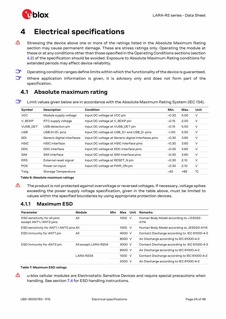
4 Electrical specifications
⚠ Stressing the device above one or more of the ratings listed in the Absolute Maximum Rating
section may cause permanent damage. These are stress ratings only. Operating the module at
these or at any conditions other than those specified in the Operating Conditions sections (section
4.2) of the specification should be avoided. Exposure to Absolute Maximum Rating conditions for
extended periods may affect device reliability.
☞ Operating condition ranges define limits within which the functionality of the device is guaranteed.
☞ Where application information is given, it is advisory only and does not form part of the
specification.
4.1 Absolute maximum rating
☞ Limit values given below are in accordance with the Absolute Maximum Rating System (IEC 134).
Symbol Description Condition Min. Max. Unit
VCC Module supply voltage Input DC voltage at VCC pin –0.30 5.00 V
V_BCKP RTC supply voltage Input DC voltage at V_BCKP pin –0.15 2.00 V
VUSB_DET USB detection pin Input DC voltage at VUSB_DET pin –0.15 5.50 V
USB USB D+/D- pins Input DC voltage at USB_D+ and USB_D- pins –1.00 5.50 V
GDI Generic digital interfaces Input DC voltage at Generic digital interfaces pins –0.30 3.60 V
HSIC HSIC interface Input DC voltage at HSIC interface pins –0.30 3.60 V
DDC DDC interface Input DC voltage at DDC interface pins –0.30 3.60 V
SIM SIM interface Input DC voltage at SIM interface pins –0.30 3.60 V
ERS External reset signal Input DC voltage at RESET_N pin –0.30 2.10 V
POS Power-on input Input DC voltage at PWR_ON pin –0.30 2.10 V
Tstg Storage Temperature –40 +85 °C
Table 6: Absolute maximum ratings
⚠ The product is not protected against overvoltage or reversed voltages. If necessary, voltage spikes
exceeding the power supply voltage specification, given in the table above, must be limited to
values within the specified boundaries by using appropriate protection devices.
4.1.1 Maximum ESD
Parameter Module Min Max Unit Remarks
ESD sensitivity for all pins
except ANT1 / ANT2 pins
All 1000 V Human Body Model according to J ESD22-
A114
ESD sensitivity for ANT1 / ANT2 pins All 1000 V Human Body Model according to JESD22-A114
ESD immunity for ANT1 pin All 4000 V Contact Discharge according to IEC 61000-4-2
8000 V Air Discharge according to IEC 61000-4-2
ESD immunity for ANT2 pin All except LARA-R204 4000 V Contact Discharge according to IEC 61000-4-2
8000 V Air Discharge according to IEC 61000-4-2
LARA-R204 1000 V Contact Discharge according to IEC 61000-4-2
2000 V Air Discharge according to IEC 61000-4-2
Table 7: Maximum ESD ratings
⚠ u-blox cellular modules are Electrostatic Sensitive Devices and require special precautions when
handling. See section 7.4 for ESD handling instructions.
LARA-R2 series - Data Sheet
UBX-16005783 - R15 Electrical specifications Page 25 of 48
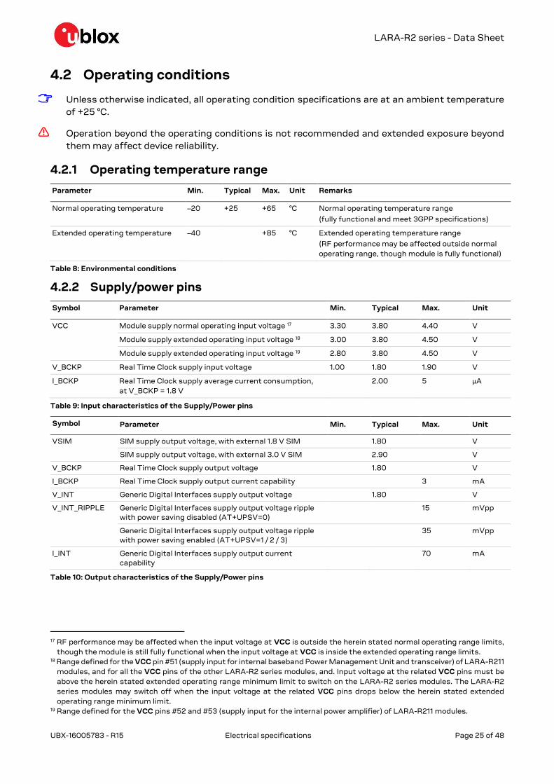
4.2 Operating conditions
☞ Unless otherwise indicated, all operating condition specifications are at an ambient temperature
of +25 °C.
⚠ Operation beyond the operating conditions is not recommended and extended exposure beyond
them may affect device reliability.
4.2.1 Operating temperature range
Parameter Min. Typical Max. Unit Remarks
Normal operating temperature –20 +25 +65 °C Normal operating temperature range
(fully functional and meet 3GPP specifications)
Extended operating temperature –40 +85 °C Extended operating temperature range
(RF performance may be affected outside normal
operating range, though module is fully functional)
Table 8: Environmental conditions
4.2.2 Supply/power pins
Symbol Parameter Min. Typical Max. Unit
VCC Module supply normal operating input voltage 17 3.30 3.80 4.40 V
Module supply extended operating input voltage 18 3.00 3.80 4.50 V
Module supply extended operating input voltage 19 2.80 3.80 4.50 V
V_BCKP Real Time Clock supply input voltage 1.00 1.80 1.90 V
I_BCKP Real Time Clock supply average current consumption,
at V_BCKP = 1.8 V
2.00 5 µA
Table 9: Input characteristics of the Supply/Power pins
Symbol Parameter Min. Typical Max. Unit
VSIM SIM supply output voltage, with external 1.8 V SIM 1.80 V
SIM supply output voltage, with external 3.0 V SIM 2.90 V
V_BCKP Real Time Clock supply output voltage 1.80 V
I_BCKP Real Time Clock supply output current capability 3 mA
V_INT Generic Digital Interfaces supply output voltage 1.80 V
V_INT_RIPPLE Generic Digital Interfaces supply output voltage ripple
with power saving disabled (AT+UPSV=0)
15 mVpp
Generic Digital Interfaces supply output voltage ripple
with power saving enabled (AT+UPSV=1 / 2 / 3)
35 mVpp
I_INT Generic Digital Interfaces supply output current
capability
70 mA
Table 10: Output characteristics of the Supply/Power pins
17 RF performance may be affected when the input voltage at VCC is outside the herein stated normal operating range limits,
though the module is still fully functional when the input voltage at VCC is inside the extended operating range limits. 18 Range defined for the VCC pin #51 (supply input for internal baseband Power Management Unit and transceiver) of LARA-R211
modules, and for all the VCC pins of the other LARA-R2 series modules, and. Input voltage at the related VCC pins must be
above the herein stated extended operating range minimum limit to switch on the LARA-R2 series modules. The LARA-R2
series modules may switch off when the input voltage at the related VCC pins drops below the herein stated extended
operating range minimum limit. 19 Range defined for the VCC pins #52 and #53 (supply input for the internal power amplifier) of LARA-R211 modules.
LARA-R2 series - Data Sheet
UBX-16005783 - R15 Electrical specifications Page 26 of 48
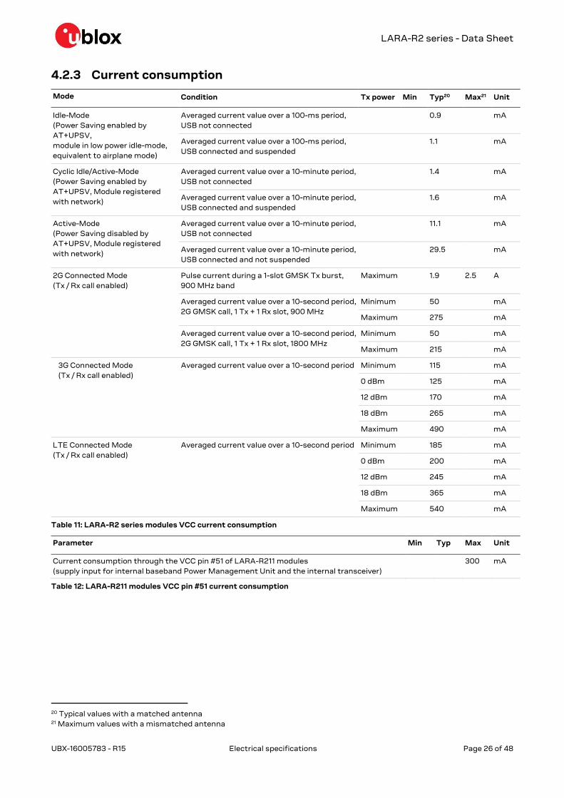
4.2.3 Current consumption
Mode Condition Tx power Min Typ20 Max21 Unit
Idle-Mode
(Power Saving enabled by
AT+UPSV,
module in low power idle-mode,
equivalent to airplane mode)
Averaged current value over a 100-ms period,
USB not connected
0.9 mA
Averaged current value over a 100-ms period,
USB connected and suspended
1.1 mA
Cyclic Idle/Active-Mode
(Power Saving enabled by
AT+UPSV, Module registered
with network)
Averaged current value over a 10-minute period,
USB not connected
1.4 mA
Averaged current value over a 10-minute period,
USB connected and suspended
1.6 mA
Active-Mode
(Power Saving disabled by
AT+UPSV, Module registered
with network)
Averaged current value over a 10-minute period,
USB not connected
11.1 mA
Averaged current value over a 10-minute period,
USB connected and not suspended
29.5 mA
2G Connected Mode
(Tx / Rx call enabled)
Pulse current during a 1-slot GMSK Tx burst,
900 MHz band
Maximum 1.9 2.5 A
Averaged current value over a 10-second period,
2G GMSK call, 1 Tx + 1 Rx slot, 900 MHz
Minimum 50 mA
Maximum 275 mA
Averaged current value over a 10-second period,
2G GMSK call, 1 Tx + 1 Rx slot, 1800 MHz
Minimum 50 mA
Maximum 215 mA
3G Connected Mode
(Tx / Rx call enabled)
Averaged current value over a 10-second period Minimum 115 mA
0 dBm 125 mA
12 dBm 170 mA
18 dBm 265 mA
Maximum 490 mA
LTE Connected Mode
(Tx / Rx call enabled)
Averaged current value over a 10-second period Minimum 185 mA
0 dBm 200 mA
12 dBm 245 mA
18 dBm 365 mA
Maximum 540 mA
Table 11: LARA-R2 series modules VCC current consumption
Parameter Min Typ Max Unit
Current consumption through the VCC pin #51 of LARA-R211 modules
(supply input for internal baseband Power Management Unit and the internal transceiver)
300 mA
Table 12: LARA-R211 modules VCC pin #51 current consumption
20 Typical values with a matched antenna 21 Maximum values with a mismatched antenna
LARA-R2 series - Data Sheet
UBX-16005783 - R15 Electrical specifications Page 27 of 48
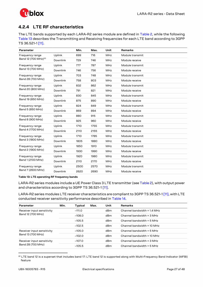
4.2.4 LTE RF characteristics
The LTE bands supported by each LARA-R2 series module are defined in Table 2, while the following
Table 13 describes the Transmitting and Receiving frequencies for each LTE band according to 3GPP
TS 36.521-1 [11].
Parameter Min. Max. Unit Remarks
Frequency range
Band 12 (700 MHz)22
Uplink 699 716 MHz Module transmit
Downlink 729 746 MHz Module receive
Frequency range
Band 13 (700 MHz)
Uplink 777 787 MHz Module transmit
Downlink 746 756 MHz Module receive
Frequency range
Band 28 (700 MHz)
Uplink 703 748 MHz Module transmit
Downlink 758 803 MHz Module receive
Frequency range
Band 20 (800 MHz)
Uplink 832 862 MHz Module transmit
Downlink 791 821 MHz Module receive
Frequency range
Band 19 (850 MHz)
Uplink 830 845 MHz Module transmit
Downlink 875 890 MHz Module receive
Frequency range
Band 5 (850 MHz)
Uplink 824 849 MHz Module transmit
Downlink 869 894 MHz Module receive
Frequency range
Band 8 (900 MHz)
Uplink 880 915 MHz Module transmit
Downlink 925 960 MHz Module receive
Frequency range
Band 4 (1700 MHz)
Uplink 1710 1755 MHz Module transmit
Downlink 2110 2155 MHz Module receive
Frequency range
Band 3 (1800 MHz)
Uplink 1710 1785 MHz Module transmit
Downlink 1805 1880 MHz Module receive
Frequency range
Band 2 (1900 MHz)
Uplink 1850 1910 MHz Module transmit
Downlink 1930 1990 MHz Module receive
Frequency range
Band 1 (2100 MHz)
Uplink 1920 1980 MHz Module transmit
Downlink 2110 2170 MHz Module receive
Frequency range
Band 7 (2600 MHz)
Uplink 2500 2570 MHz Module transmit
Downlink 2620 2690 MHz Module receive
Table 13: LTE operating RF frequency bands
LARA-R2 series modules include a UE Power Class 3 LTE transmitter (see Table 2), with output power
and characteristics according to 3GPP TS 36.521-1 [11].
LARA-R2 series modules LTE receiver characteristics are compliant to 3GPP TS 36.521-1 [11], with LTE
conducted receiver sensitivity performance described in Table 14.
Parameter Min. Typical Max. Unit Remarks
Receiver input sensitivity
Band 12 (700 MHz)
–111.0 dBm Channel bandwidth = 1.4 MHz
–108.0 dBm Channel bandwidth = 3 MHz
–105.5 dBm Channel bandwidth = 5 MHz
–102.5 dBm Channel bandwidth = 10 MHz
Receiver input sensitivity
Band 13 (700 MHz)
–105.0 dBm Channel bandwidth = 5 MHz
–102.0 dBm Channel bandwidth = 10 MHz
Receiver input sensitivity
Band 28 (700 MHz)
–107.0 dBm Channel bandwidth = 3 MHz
–105.5 dBm Channel bandwidth = 5 MHz
22 LTE band 12 is a superset that includes band 17: LTE band 12 is supported along with Multi-Frequency Band Indicator (MFBI)
feature
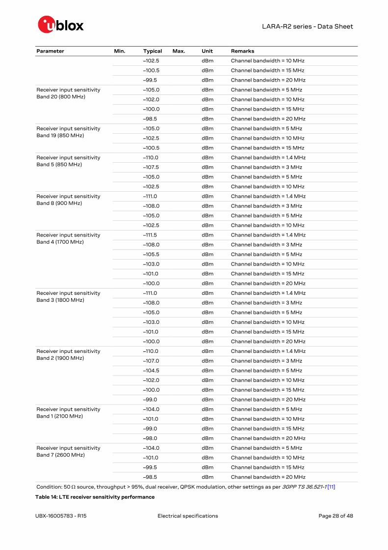
LARA-R2 series - Data Sheet
UBX-16005783 - R15 Electrical specifications Page 28 of 48
Parameter Min. Typical Max. Unit Remarks
–102.5 dBm Channel bandwidth = 10 MHz
–100.5 dBm Channel bandwidth = 15 MHz
–99.5 dBm Channel bandwidth = 20 MHz
Receiver input sensitivity
Band 20 (800 MHz)
–105.0 dBm Channel bandwidth = 5 MHz
–102.0 dBm Channel bandwidth = 10 MHz
–100.0 dBm Channel bandwidth = 15 MHz
–98.5 dBm Channel bandwidth = 20 MHz
Receiver input sensitivity
Band 19 (850 MHz)
–105.0 dBm Channel bandwidth = 5 MHz
–102.5 dBm Channel bandwidth = 10 MHz
–100.5 dBm Channel bandwidth = 15 MHz
Receiver input sensitivity
Band 5 (850 MHz)
–110.0 dBm Channel bandwidth = 1.4 MHz
–107.5 dBm Channel bandwidth = 3 MHz
–105.0 dBm Channel bandwidth = 5 MHz
–102.5 dBm Channel bandwidth = 10 MHz
Receiver input sensitivity
Band 8 (900 MHz)
–111.0 dBm Channel bandwidth = 1.4 MHz
–108.0 dBm Channel bandwidth = 3 MHz
–105.0 dBm Channel bandwidth = 5 MHz
–102.5 dBm Channel bandwidth = 10 MHz
Receiver input sensitivity
Band 4 (1700 MHz)
–111.5 dBm Channel bandwidth = 1.4 MHz
–108.0 dBm Channel bandwidth = 3 MHz
–105.5 dBm Channel bandwidth = 5 MHz
–103.0 dBm Channel bandwidth = 10 MHz
–101.0 dBm Channel bandwidth = 15 MHz
–100.0 dBm Channel bandwidth = 20 MHz
Receiver input sensitivity
Band 3 (1800 MHz)
–111.0 dBm Channel bandwidth = 1.4 MHz
–108.0 dBm Channel bandwidth = 3 MHz
–105.0 dBm Channel bandwidth = 5 MHz
–103.0 dBm Channel bandwidth = 10 MHz
–101.0 dBm Channel bandwidth = 15 MHz
–100.0 dBm Channel bandwidth = 20 MHz
Receiver input sensitivity
Band 2 (1900 MHz)
–110.0 dBm Channel bandwidth = 1.4 MHz
–107.0 dBm Channel bandwidth = 3 MHz
–104.5 dBm Channel bandwidth = 5 MHz
–102.0 dBm Channel bandwidth = 10 MHz
–100.0 dBm Channel bandwidth = 15 MHz
–99.0 dBm Channel bandwidth = 20 MHz
Receiver input sensitivity
Band 1 (2100 MHz)
–104.0 dBm Channel bandwidth = 5 MHz
–101.0 dBm Channel bandwidth = 10 MHz
–99.0 dBm Channel bandwidth = 15 MHz
–98.0 dBm Channel bandwidth = 20 MHz
Receiver input sensitivity
Band 7 (2600 MHz)
–104.0 dBm Channel bandwidth = 5 MHz
–101.0 dBm Channel bandwidth = 10 MHz
–99.5 dBm Channel bandwidth = 15 MHz
–98.5 dBm Channel bandwidth = 20 MHz
Condition: 50 source, throughput > 95%, dual receiver, QPSK modulation, other settings as per 3GPP TS 36.521-1 [11]
Table 14: LTE receiver sensitivity performance
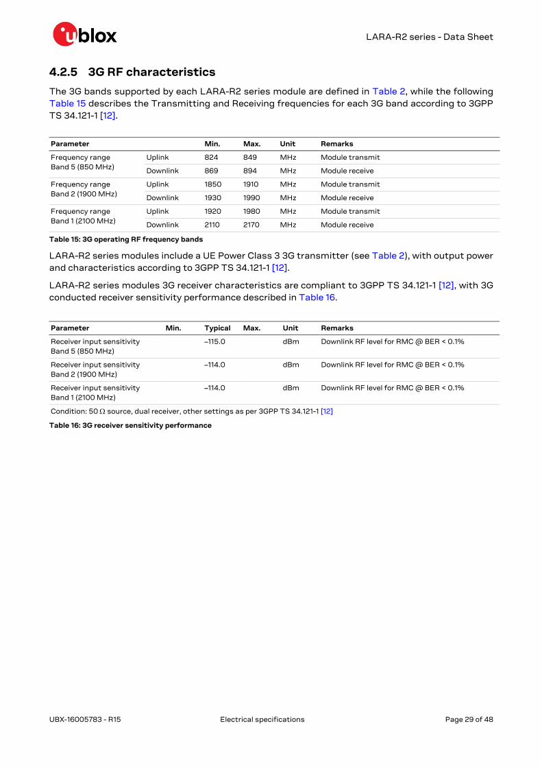
LARA-R2 series - Data Sheet
UBX-16005783 - R15 Electrical specifications Page 29 of 48
4.2.5 3G RF characteristics
The 3G bands supported by each LARA-R2 series module are defined in Table 2, while the following
Table 15 describes the Transmitting and Receiving frequencies for each 3G band according to 3GPP
TS 34.121-1 [12].
Parameter Min. Max. Unit Remarks
Frequency range
Band 5 (850 MHz)
Uplink 824 849 MHz Module transmit
Downlink 869 894 MHz Module receive
Frequency range
Band 2 (1900 MHz)
Uplink 1850 1910 MHz Module transmit
Downlink 1930 1990 MHz Module receive
Frequency range
Band 1 (2100 MHz)
Uplink 1920 1980 MHz Module transmit
Downlink 2110 2170 MHz Module receive
Table 15: 3G operating RF frequency bands
LARA-R2 series modules include a UE Power Class 3 3G transmitter (see Table 2), with output power
and characteristics according to 3GPP TS 34.121-1 [12].
LARA-R2 series modules 3G receiver characteristics are compliant to 3GPP TS 34.121-1 [12], with 3G
conducted receiver sensitivity performance described in Table 16.
Parameter Min. Typical Max. Unit Remarks
Receiver input sensitivity
Band 5 (850 MHz)
–115.0 dBm Downlink RF level for RMC @ BER < 0.1%
Receiver input sensitivity
Band 2 (1900 MHz)
–114.0 dBm Downlink RF level for RMC @ BER < 0.1%
Receiver input sensitivity
Band 1 (2100 MHz)
–114.0 dBm Downlink RF level for RMC @ BER < 0.1%
Condition: 50 source, dual receiver, other settings as per 3GPP TS 34.121-1 [12]
Table 16: 3G receiver sensitivity performance
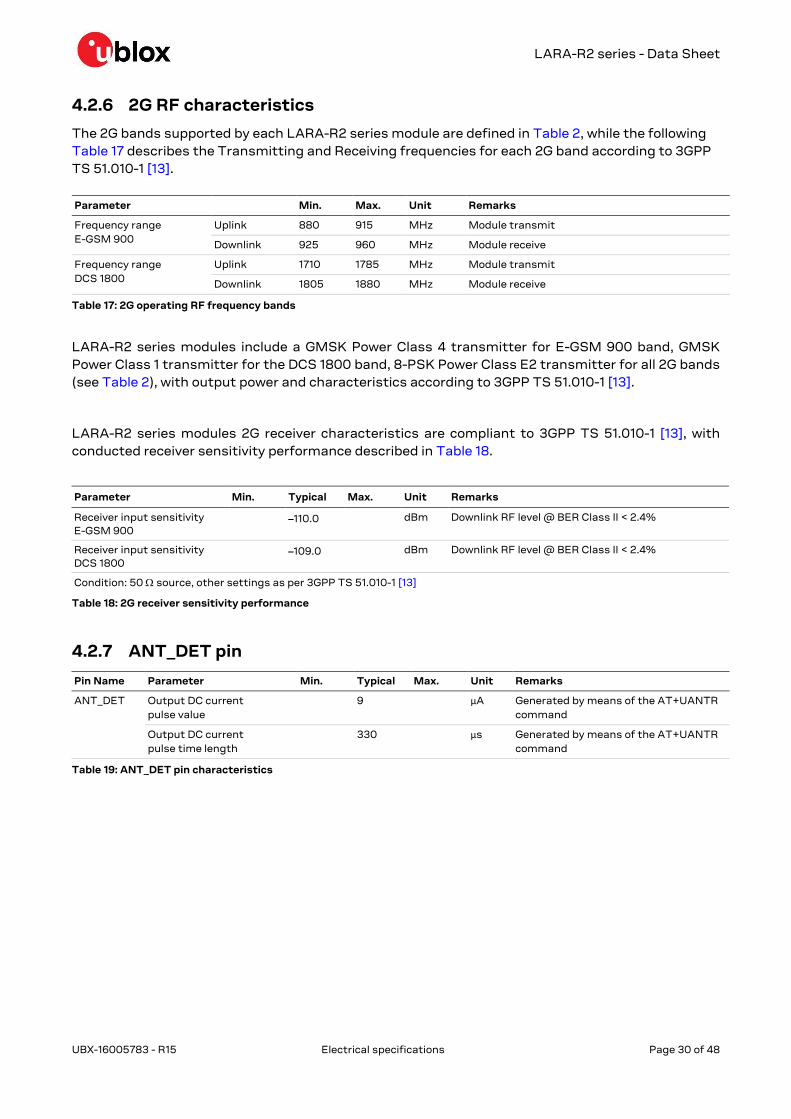
LARA-R2 series - Data Sheet
UBX-16005783 - R15 Electrical specifications Page 30 of 48
4.2.6 2G RF characteristics
The 2G bands supported by each LARA-R2 series module are defined in Table 2, while the following
Table 17 describes the Transmitting and Receiving frequencies for each 2G band according to 3GPP
TS 51.010-1 [13].
Parameter Min. Max. Unit Remarks
Frequency range
E-GSM 900
Uplink 880 915 MHz Module transmit
Downlink 925 960 MHz Module receive
Frequency range
DCS 1800
Uplink 1710 1785 MHz Module transmit
Downlink 1805 1880 MHz Module receive
Table 17: 2G operating RF frequency bands
LARA-R2 series modules include a GMSK Power Class 4 transmitter for E-GSM 900 band, GMSK
Power Class 1 transmitter for the DCS 1800 band, 8-PSK Power Class E2 transmitter for all 2G bands
(see Table 2), with output power and characteristics according to 3GPP TS 51.010-1 [13].
LARA-R2 series modules 2G receiver characteristics are compliant to 3GPP TS 51.010-1 [13], with
conducted receiver sensitivity performance described in Table 18.
Parameter Min. Typical Max. Unit Remarks
Receiver input sensitivity
E-GSM 900
–110.0 dBm Downlink RF level @ BER Class II < 2.4%
Receiver input sensitivity
DCS 1800
–109.0 dBm Downlink RF level @ BER Class II < 2.4%
Condition: 50 source, other settings as per 3GPP TS 51.010-1 [13]
Table 18: 2G receiver sensitivity performance
4.2.7 ANT_DET pin
Pin Name Parameter Min. Typical Max. Unit Remarks
ANT_DET Output DC current
pulse value
9 µA Generated by means of the AT+UANTR
command
Output DC current
pulse time length
330 µs Generated by means of the AT+UANTR
command
Table 19: ANT_DET pin characteristics
LARA-R2 series - Data Sheet
UBX-16005783 - R15 Electrical specifications Page 31 of 48
4.2.8 PWR_ON pin
Pin Name Parameter Min. Typical Max. Unit Remarks
PWR_ON Internal supply for
Power-On Input Signal
1.80 V RTC supply (V_BCKP)
Low-level input –0.30 0.54 V
High-level input 1.26 2.10 V
Pull-up resistance 10 k Internal active pull-up to V_BCKP
Low-level input current –180 µA
Low pulse time 50 µs Low pulse time to switch on the module
Low pulse time 1 s Low pulse time to switch off the module
Table 20: PWR_ON pin characteristics
4.2.9 RESET_N pin
Pin Name Parameter Min. Typical Max. Unit Remarks
RESET_N Internal supply for
External Reset Input Signal
1.80 V RTC supply (V_BCKP)
Low-level input –0.30 0.54 V
High-level input 1.26 2.10 V
Pull-up resistance 10 k Internal active pull-up to V_BCKP
Low-level input current –180 µA
Low pulse time 50 ms Low pulse time to reset the module
Table 21: RESET_N pin characteristics
4.2.10 SIM pins
The SIM pins are a dedicated interface to the external SIM card/chip. The electrical characteristics
fulfill the regulatory specification requirements. The values in Table 22 are for information only.
Parameter Min. Typical Max. Unit Remarks
Low-level input 0.00 0.35 V VSIM = 1.80 V
0.00 0.57 V VSIM = 2.90 V
High-level input 1.29 3.30 V VSIM = 1.80 V
2.07 3.30 V VSIM = 2.90 V
Low-level output 0.00 0.35 V VSIM = 1.80 V, Max value at IOL = +1.0 mA
0.00 0.35 V VSIM = 2.90 V, Max value at IOL = +1.0 mA
High-level output 1.26 1.80 V VSIM = 1.80 V, Min value at IOH = –1.0 mA
2.03 2.90 V VSIM = 2.90 V, Min value at IOH = –1.0 mA
Input / Output leakage current 0.7 µA 0.2V < VIN < 3.3V
Clock frequency on SIM_CLK 3.25 MHz
Internal pull-up resistor on SIM_IO 4.7 k Internal pull-up to VSIM supply
Table 22: SIM pins characteristics
LARA-R2 series - Data Sheet
UBX-16005783 - R15 Electrical specifications Page 32 of 48
4.2.11 USB pins
USB data lines (USB_D+ / USB_D–) are compliant with the USB 2.0 high-speed specification. See the
Universal Serial Bus Specification Revision 2.0 [15] for detailed electrical characteristics. The values
in Table 23 related to USB 2.0 high-speed physical layer specifications are for information only.
Parameter Min. Typical Max. Unit Remarks
VUSB_DET pin, High-level input 1.50 5.00 5.25 V
VUSB_DET pin, Low-level input –0.15 0.00 0.40 V
VUSB_DET pin, input current sink 25 µA
High-speed squelch detection threshold
(input differential signal amplitude)
100 150 mV
High speed disconnect detection threshold
(input differential signal amplitude)
525 625 mV
High-speed data signaling input
common mode voltage range
–50 500 mV
High-speed idle output level –10 10 mV
High-speed data signaling output high level 360 440 mV
High-speed data signaling output low level –10 10 mV
Chirp J level (output differential voltage) 700 1100 mV
Chirp K level (output differential voltage) –900 –500 mV
Table 23: USB pins characteristics
4.2.12 HSIC pins
The HSIC USB lines (HSIC_DATA / HSIC_STRB) are compliant with the High-Speed Inter-Chip USB
specification. See the High-Speed Inter-Chip USB Electrical Specification Version 1.0 [16] and the USB
Specification Revision 2.0 [15] for detailed electrical characteristics. The values in Table 24 related to
the High-Speed Inter-Chip USB electrical specifications are for information only.
Parameter Min Typical Max Unit Remarks
Internal supply for HSIC domain 1.20 V
Low-level input –0.30 0.42 V
High-level input 0.78 1.50 V
Low-level output 0.00 0.30 V Max value at IOL = +2.0 mA
High-level output 0.90 1.20 V Min value at IOH = –2.0 mA
Input/output leakage current 0.7 µA 0.2V < VIN < 1.5V
Table 24: HSIC pins characteristics
LARA-R2 series - Data Sheet
UBX-16005783 - R15 Electrical specifications Page 33 of 48
4.2.13 DDC (I2C) pins
DDC (I2C) lines (SCL and SDA) are compliant with the I2C-bus standard mode specification. See the
I2C-Bus Specification [17] for detailed electrical characteristics. The values in Table 25 related to
I2C-bus standard mode specifications are for information only.
Parameter Min Typical Max Unit Remarks
Internal supply for GDI domain 1.80 V Digital I/O Interfaces supply (V_INT)
Low-level input –0.20 0.36 V
High-level input 1.26 2.00 V
Low-level output 0.00 0.35 V Max value at IOL = +1.0 mA
Clock frequency on SCL 100 kHz
Table 25: DDC (I2C) pins characteristics
4.2.14 Generic Digital Interfaces pins
Parameter Min Typical Max Unit Remarks
Internal supply for GDI domain 1.80 V Digital I/O Interfaces supply (V_INT)
Low-level input –0.20 0.36 V
High-level input 1.26 2.00 V
Low-level output 0.00 0.35 V Max value at IOL = +6.0 mA for driver class A
High-level output 1.45 1.80 V Min value at IOH = –6.0 mA for driver class A
Internal pull-up input current –240 µA PU class a
–110 µA PU class b
Internal pull-down input current 240 µA PD class a
100 µA PD class b
Input/output leakage current 0.7 µA 0.2V < VIN < 2.0V
Table 26: GDI pins characteristics
4.2.14.1 AC characteristics of clock output pin
Parameter Description Min Typical Max Unit Remarks
1/T1 GPIO6 clock output frequency 13 MHz AT+UMCLK=2
26 MHz AT+UMCLK=3
Table 27: AC characteristics of GPIO6 clock output pin
LARA-R2 series - Data Sheet
UBX-16005783 - R15 Electrical specifications Page 34 of 48
4.2.14.2 AC characteristics of I2S pins
Parameter Description Min Typical Max Unit Remarks
1/T1 I2S_WA frequency 8.000 kHz <I2S_sample_rate>=0
11.025 kHz <I2S_sample_rate>=1
12.000 kHz <I2S_sample_rate>=2
16.000 kHz <I2S_sample_rate>=3
22.050 kHz <I2S_sample_rate>=4
24.000 kHz <I2S_sample_rate>=5
32.000 kHz <I2S_sample_rate>=6
44.100 kHz <I2S_sample_rate>=7
48.000 kHz <I2S_sample_rate>=8
1/T2 I2S_CLK frequency 32 1/T1 <I2S_mode> = 2,..,13
T3 I2S_TXD invalid before I2S_CLK edge 24 ns <I2S_mode> = 2,..,13
T4 I2S_TXD valid after I2S_CLK edge 32 ns <I2S_mode> = 2,..,13
T5 I2S_RXD setup time before I2S_CLK edge 60 ns <I2S_mode> = 2,..,13
T6 I2S_RXD hold time after I2S_CLK edge 10 ns <I2S_mode> = 2,..,13
Table 28: AC characteristics of digital audio interface (I2S) pins in Normal I2S mode (long synchronization signal), Master role
Parameter Description Min Typical Max Unit Remarks
1/T1 I2S_WA frequency 8.000 kHz <I2S_sample_rate>=0
11.025 kHz <I2S_sample_rate>=1
12.000 kHz <I2S_sample_rate>=2
16.000 kHz <I2S_sample_rate>=3
22.050 kHz <I2S_sample_rate>=4
24.000 kHz <I2S_sample_rate>=5
32.000 kHz <I2S_sample_rate>=6
44.100 kHz <I2S_sample_rate>=7
48.000 kHz <I2S_sample_rate>=8
1/T2 I2S_CLK frequency 32 1/T1 <I2S_mode> = 2,..,13
T3 I2S_TXD invalid before I2S_CLK edge 12 ns <I2S_mode> = 2,..,13
T4 I2S_TXD valid after I2S_CLK edge 79 ns <I2S_mode> = 2,..,13
T5 I2S_RXD setup time before I2S_CLK edge 22 ns <I2S_mode> = 2,..,13
T6 I2S_RXD hold time after I2S_CLK edge 24 ns <I2S_mode> = 2,..,13
Table 29: AC characteristics of digital audio interface (I2S) pins in Normal I2S mode (long synchronization signal), Slave role
LARA-R2 series - Data Sheet
UBX-16005783 - R15 Electrical specifications Page 35 of 48
Parameter Description Min Typical Max Unit Remarks
1/T1 I2S_WA frequency 8.000 kHz <I2S_sample_rate>=0
11.025 kHz <I2S_sample_rate>=1
12.000 kHz <I2S_sample_rate>=2
16.000 kHz <I2S_sample_rate>=3
22.050 kHz <I2S_sample_rate>=4
24.000 kHz <I2S_sample_rate>=5
32.000 kHz <I2S_sample_rate>=6
44.100 kHz <I2S_sample_rate>=7
48.000 kHz <I2S_sample_rate>=8
1/T2 I2S_CLK frequency 18 1/T1 <I2S_mode> = 0
17 1/T1 <I2S_mode> = 1
T3 I2S_WA high begin after I2S_CLK high begin -24 32 ns <I2S_mode> = 0, 1
T4 I2S_WA high end after I2S_CLK low end -24 32 ns <I2S_mode> = 0, 1
T5 I2S_TXD invalid before I2S_CLK low end 24 ns <I2S_mode> = 0, 1
T6 I2S_TXD valid after I2S_CLK high begin 22 ns <I2S_mode> = 0, 1
T7 I2S_RXD setup time before I2S_CLK high end 60 ns <I2S_mode> = 0, 1
T8 I2S_RXD hold time after I2S_CLK low begin 12 ns <I2S_mode> = 0, 1
Table 30: AC characteristics of digital audio interface (I2S) pins in PCM mode (short synchronization signal), Master role
Parameter Description Min Typical Max Unit Remarks
1/T1 I2S_WA frequency 8.000 kHz <I2S_sample_rate>=0
11.025 kHz <I2S_sample_rate>=1
12.000 kHz <I2S_sample_rate>=2
16.000 kHz <I2S_sample_rate>=3
22.050 kHz <I2S_sample_rate>=4
24.000 kHz <I2S_sample_rate>=5
32.000 kHz <I2S_sample_rate>=6
44.100 kHz <I2S_sample_rate>=7
48.000 kHz <I2S_sample_rate>=8
1/T2 I2S_CLK frequency 18 1/T1 <I2S_mode> = 0
17 1/T1 <I2S_mode> = 1
T3 I2S_WA high begin before I2S_CLK low begin 36 ns <I2S_mode> = 0, 1
T4 I2S_WA low begin before I2S_CLK low begin 36 ns <I2S_mode> = 0, 1
T5 I2S_TXD invalid before I2S_CLK rising edge 12 ns <I2S_mode> = 0, 1
T6 I2S_TXD valid after I2S_CLK rising edge 79 ns <I2S_mode> = 0, 1
T7 I2S_RXD setup time before I2S_CLK falling
edge
22 ns <I2S_mode> = 0, 1
T8 I2S_RXD hold time after I2S_CLK falling edge 24 ns <I2S_mode> = 0, 1
Table 31: AC characteristics of digital audio interface (I2S) pins in PCM mode (short synchronization signal), Slave role
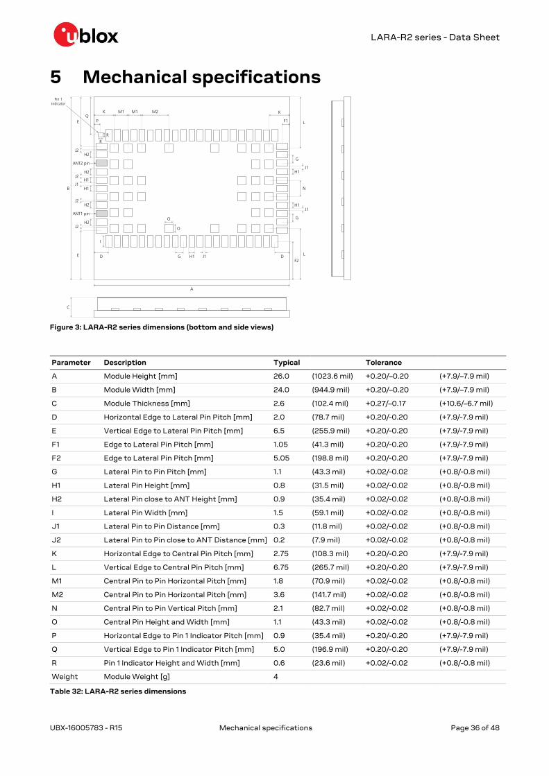
LARA-R2 series - Data Sheet
UBX-16005783 - R15 Mechanical specifications Page 36 of 48
5 Mechanical specifications
C
R
R
PQ
K M1 M1 M2
E
H1J1
H2J2
J2H2
E
ANT1 pin
B
Pin 1 Indicator
K
G H1 J1D
A
D
O
O
L
N
L
I
F1
F2
ANT2 pinG
G
H1J1
H1J1
H2J2
J2H2
H1
Figure 3: LARA-R2 series dimensions (bottom and side views)
Parameter Description Typical Tolerance
A Module Height [mm] 26.0 (1023.6 mil) +0.20/–0.20 (+7.9/–7.9 mil)
B Module Width [mm] 24.0 (944.9 mil) +0.20/–0.20 (+7.9/–7.9 mil)
C Module Thickness [mm] 2.6 (102.4 mil) +0.27/–0.17 (+10.6/–6.7 mil)
D Horizontal Edge to Lateral Pin Pitch [mm] 2.0 (78.7 mil) +0.20/-0.20 (+7.9/-7.9 mil)
E Vertical Edge to Lateral Pin Pitch [mm] 6.5 (255.9 mil) +0.20/-0.20 (+7.9/-7.9 mil)
F1 Edge to Lateral Pin Pitch [mm] 1.05 (41.3 mil) +0.20/-0.20 (+7.9/-7.9 mil)
F2 Edge to Lateral Pin Pitch [mm] 5.05 (198.8 mil) +0.20/-0.20 (+7.9/-7.9 mil)
G Lateral Pin to Pin Pitch [mm] 1.1 (43.3 mil) +0.02/-0.02 (+0.8/-0.8 mil)
H1 Lateral Pin Height [mm] 0.8 (31.5 mil) +0.02/-0.02 (+0.8/-0.8 mil)
H2 Lateral Pin close to ANT Height [mm] 0.9 (35.4 mil) +0.02/-0.02 (+0.8/-0.8 mil)
I Lateral Pin Width [mm] 1.5 (59.1 mil) +0.02/-0.02 (+0.8/-0.8 mil)
J1 Lateral Pin to Pin Distance [mm] 0.3 (11.8 mil) +0.02/-0.02 (+0.8/-0.8 mil)
J2 Lateral Pin to Pin close to ANT Distance [mm] 0.2 (7.9 mil) +0.02/-0.02 (+0.8/-0.8 mil)
K Horizontal Edge to Central Pin Pitch [mm] 2.75 (108.3 mil) +0.20/-0.20 (+7.9/-7.9 mil)
L Vertical Edge to Central Pin Pitch [mm] 6.75 (265.7 mil) +0.20/-0.20 (+7.9/-7.9 mil)
M1 Central Pin to Pin Horizontal Pitch [mm] 1.8 (70.9 mil) +0.02/-0.02 (+0.8/-0.8 mil)
M2 Central Pin to Pin Horizontal Pitch [mm] 3.6 (141.7 mil) +0.02/-0.02 (+0.8/-0.8 mil)
N Central Pin to Pin Vertical Pitch [mm] 2.1 (82.7 mil) +0.02/-0.02 (+0.8/-0.8 mil)
O Central Pin Height and Width [mm] 1.1 (43.3 mil) +0.02/-0.02 (+0.8/-0.8 mil)
P Horizontal Edge to Pin 1 Indicator Pitch [mm] 0.9 (35.4 mil) +0.20/-0.20 (+7.9/-7.9 mil)
Q Vertical Edge to Pin 1 Indicator Pitch [mm] 5.0 (196.9 mil) +0.20/-0.20 (+7.9/-7.9 mil)
R Pin 1 Indicator Height and Width [mm] 0.6 (23.6 mil) +0.02/-0.02 (+0.8/-0.8 mil)
Weight Module Weight [g] 4
Table 32: LARA-R2 series dimensions
LARA-R2 series - Data Sheet
UBX-16005783 - R15 Mechanical specifications Page 37 of 48
☞ Module Height tolerance +/–0.20 mm may be exceeded close to the corners of the PCB due to the
cutting process. In the worst case, the height could be +0.40 mm more than the typical value.
☞ For information regarding Footprint and Paste Mask recommended for the application board
integrating the cellular module, see the LARA-R2 series System Integration Manual [2].
LARA-R2 series - Data Sheet
UBX-16005783 - R15 Qualification and approvals Page 38 of 48
6 Qualification and approvals
6.1 Reliability tests
Tests for product family qualifications according to ISO 16750 “Road vehicles – Environmental
conditions and testing for electrical and electronic equipment“, and appropriate standards.
6.2 Approvals
Products marked with this lead-free symbol on the product label comply with the
"Directive 2002/95/EC of the European Parliament and the Council on the
Restriction of Use of certain Hazardous Substances in Electrical and Electronic
Equipment" (RoHS).
LARA-R2 series modules are RoHS compliant.
No natural rubbers, hygroscopic materials, or materials containing asbestos are
employed.
Table 33 summarizes the main approvals for LARA-R2 series modules.
Certification Scheme LARA-R202 LARA-R203 LARA-R204 LARA-R211 LARA-R220 LARA-R280
GCF • •
PTCRB • •
CE (Europe) •
FCC (United States)
FCC identification number
•
XPY1EIQ24NN
•
XPY1DIQN3NN
•
XPY1EIQN2NN
ISED (Canada) 23
IC certification number
•
8595A-1EIQ24NN
•
8595A-1DIQN3NN
•
8595A-1EIQN2NN
Giteki (Japan) •
RCM (Australia) •
NCC (Taiwan) •
AT&T (US MNO) • •
T-Mobile (US MNO) •
Verizon (US MNO) •
Vodafone (MNO) •
NTT DoCoMo
(Japanese MNO)
•
Table 33: LARA-R2 series main certification approvals summary
For the complete list of approvals and for specific details on all country and network operators’
certifications, see our website www.u-blox.com or please contact the u-blox office or sales
representative nearest you.
23 Formerly known as IC (Industry Canada)
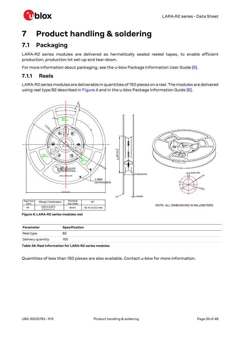
LARA-R2 series - Data Sheet
UBX-16005783 - R15 Product handling & soldering Page 39 of 48
7 Product handling & soldering
7.1 Packaging
LARA-R2 series modules are delivered as hermetically sealed reeled tapes, to enable efficient
production, production lot set-up and tear-down.
For more information about packaging, see the u-blox Package Information User Guide [6].
7.1.1 Reels
LARA-R2 series modules are deliverable in quantities of 150 pieces on a reel. The modules are delivered
using reel type B2 described in Figure 4 and in the u-blox Package Information Guide [6].
Figure 4: LARA-R2 series modules reel
Parameter Specification
Reel type B2
Delivery quantity 150
Table 34: Reel information for LARA-R2 series modules
Quantities of less than 150 pieces are also available. Contact u-blox for more information.
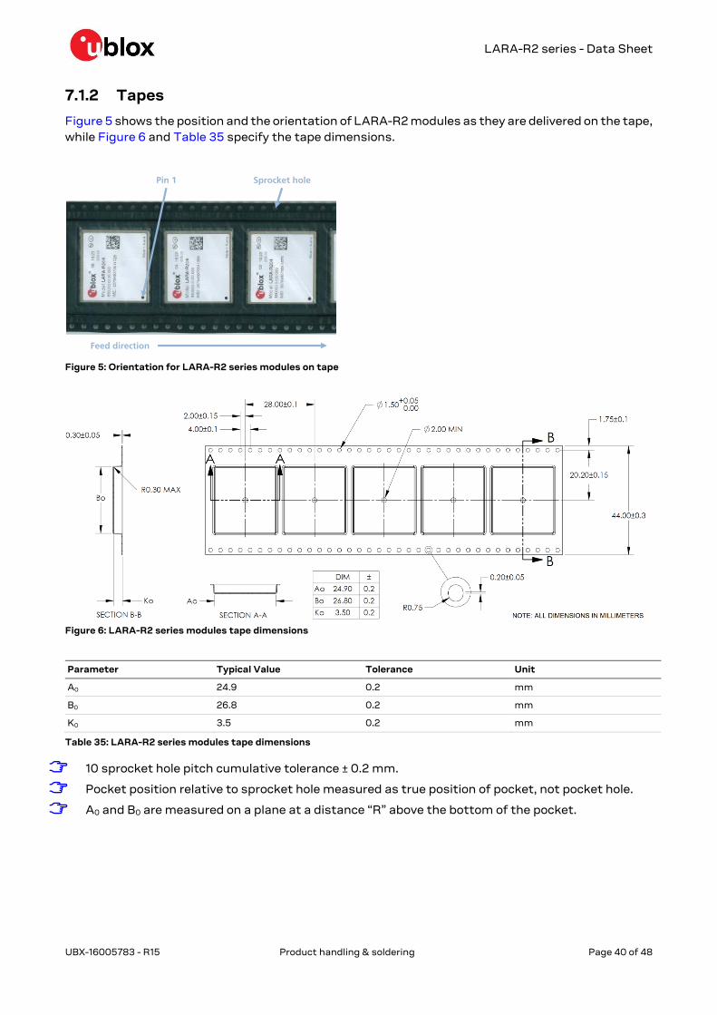
LARA-R2 series - Data Sheet
UBX-16005783 - R15 Product handling & soldering Page 40 of 48
7.1.2 Tapes
Figure 5 shows the position and the orientation of LARA-R2 modules as they are delivered on the tape,
while Figure 6 and Table 35 specify the tape dimensions.
Pin 1 Sprocket hole
Feed direction
Figure 5: Orientation for LARA-R2 series modules on tape
Figure 6: LARA-R2 series modules tape dimensions
Parameter Typical Value Tolerance Unit
A0 24.9 0.2 mm
B0 26.8 0.2 mm
K0 3.5 0.2 mm
Table 35: LARA-R2 series modules tape dimensions
☞ 10 sprocket hole pitch cumulative tolerance ± 0.2 mm.
☞ Pocket position relative to sprocket hole measured as true position of pocket, not pocket hole.
☞ A0 and B0 are measured on a plane at a distance “R” above the bottom of the pocket.
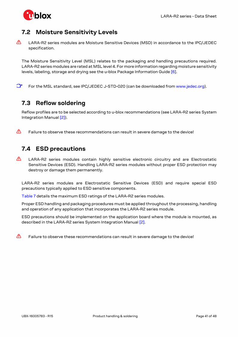
LARA-R2 series - Data Sheet
UBX-16005783 - R15 Product handling & soldering Page 41 of 48
7.2 Moisture Sensitivity Levels
⚠ LARA-R2 series modules are Moisture Sensitive Devices (MSD) in accordance to the IPC/JEDEC
specification.
The Moisture Sensitivity Level (MSL) relates to the packaging and handling precautions required.
LARA-R2 series modules are rated at MSL level 4. For more information regarding moisture sensitivity
levels, labeling, storage and drying see the u-blox Package Information Guide [6].
☞ For the MSL standard, see IPC/JEDEC J-STD-020 (can be downloaded from www.jedec.org).
7.3 Reflow soldering
Reflow profiles are to be selected according to u-blox recommendations (see LARA-R2 series System
Integration Manual [2]).
⚠ Failure to observe these recommendations can result in severe damage to the device!
7.4 ESD precautions
⚠ LARA-R2 series modules contain highly sensitive electronic circuitry and are Electrostatic
Sensitive Devices (ESD). Handling LARA-R2 series modules without proper ESD protection may
destroy or damage them permanently.
LARA-R2 series modules are Electrostatic Sensitive Devices (ESD) and require special ESD
precautions typically applied to ESD sensitive components.
Table 7 details the maximum ESD ratings of the LARA-R2 series modules.
Proper ESD handling and packaging procedures must be applied throughout the processing, handling
and operation of any application that incorporates the LARA-R2 series module.
ESD precautions should be implemented on the application board where the module is mounted, as
described in the LARA-R2 series System Integration Manual [2].
⚠ Failure to observe these recommendations can result in severe damage to the device!
LARA-R2 series - Data Sheet
UBX-16005783 - R15 Default settings Page 42 of 48
8 Default settings Interface AT settings Comments
UART interface AT interface enabled AT command mode is enabled by default on the UART physical interface
AT+IPR=0 One-shot automatic baud rate detection enabled
AT+ICF=3,1 Frame format: 8 bits, no parity, 1 stop bit
☞ Since AT+IPR=0 is the default value (one-shot automatic baud rate
detection enabled), the AT+ICF value in the profile is not applied
(AT+IPR=0 overrules the AT+ICF setting) and the one-shot automatic
frame detection is active.
AT&K3 HW flow control enabled
AT&S1 DSR line set ON in data mode and set OFF in command mode
AT&D1 Upon an ON-to-OFF transition of DTR, the module enters online command
state and issues an OK result code
AT&C1 Circuit 109 changes in accordance with the Carrier detect status; ON if the
Carrier is detected, OFF otherwise
MUX disabled Multiplexing mode can be enabled by AT+CMUX command providing
following channels:
Channel 0: Multiplexer control
Channel 1 – 5: AT commands / data connection
Channel 6: GNSS data tunneling 24
USB interface Enabled 6 USB CDCs (Communications Device Class) by default available:
USB1: AT and data
USB2: AT and data
USB3: AT and data
USB4: GNSS tunneling24
USB5: SAP (SIM Access Profile) 25
USB6: Primary Log (diagnostic purpose)
AT&K3 HW flow control enabled
AT&S1 DSR line set ON in data mode and set OFF in command mode
AT&D1 Upon an ON-to-OFF transition of DTR, the module enters online command
state and issues an OK result code
AT&C1 Circuit 109 changes in accordance with the Carrier detect status; ON if the
Carrier is detected, OFF otherwise
Power saving AT+UPSV=0 Disabled
Network registration AT+COPS=0 Self network registration
Table 36: LARA-R2 series default settings
See the u-blox AT Commands Manual [1] and the LARA-R2 series System Integration Manual [2] for
information about further settings and factory-programmed values.
24 Not supported by LARA-R204-02B and LARA-R211-02B-00 product versions. 25 Not supported by “02” and “62” product versions.
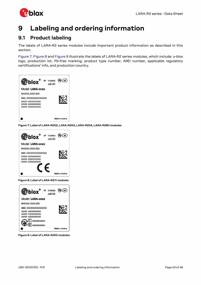
LARA-R2 series - Data Sheet
UBX-16005783 - R15 Labeling and ordering information Page 43 of 48
9 Labeling and ordering information
9.1 Product labeling
The labels of LARA-R2 series modules include important product information as described in this
section.
Figure 7, Figure 8 and Figure 9 illustrate the labels of LARA-R2 series modules, which include: u-blox
logo, production lot, Pb-free marking, product type number, IMEI number, applicable regulatory
certifications’ info, and production country.
Figure 7: Label of LARA-R202, LARA-R203, LARA-R204, LARA-R280 modules
Figure 8: Label of LARA-R211 modules
Figure 9: Label of LARA-R220 modules
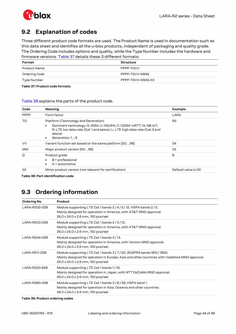
LARA-R2 series - Data Sheet
UBX-16005783 - R15 Labeling and ordering information Page 44 of 48
9.2 Explanation of codes
Three different product code formats are used. The Product Name is used in documentation such as
this data sheet and identifies all the u-blox products, independent of packaging and quality grade.
The Ordering Code includes options and quality, while the Type Number includes the hardware and
firmware versions. Table 37 details these 3 different formats:
Format Structure
Product Name PPPP-TGVV
Ordering Code PPPP-TGVV-MMQ
Type Number PPPP-TGVV-MMQ-XX
Table 37: Product code formats
Table 38 explains the parts of the product code.
Code Meaning Example
PPPP Form factor LARA
TG Platform (Technology and Generation)
Dominant technology: G: GSM; U: HSUPA; C: CDMA 1xRTT; N: NB-IoT;
R: LTE low data rate (Cat 1 and below); L: LTE high data rate (Cat.3 and
above)
Generation: 1…9
R2
VV Variant function set based on the same platform [00…99] 04
MM Major product version [00…99] 02
Q Product grade
B = professional
A = automotive
B
XX Minor product version (not relevant for certification) Default value is 00
Table 38: Part identification code
9.3 Ordering information
Ordering No. Product
LARA-R202-02B Module supporting LTE Cat 1 bands 2 / 4 / 5 / 12, HSPA bands 2 / 5.
Mainly designed for operation in America, with AT&T MNO approval.
26.0 x 24.0 x 2.6 mm, 150 pcs/reel
LARA-R203-02B Module supporting LTE Cat 1 bands 2 / 4 / 12.
Mainly designed for operation in America, with AT&T MNO approval.
26.0 x 24.0 x 2.6 mm, 150 pcs/reel
LARA-R204-02B Module supporting LTE Cat 1 bands 4 / 13.
Mainly designed for operation in America, with Verizon MNO approval.
26.0 x 24.0 x 2.6 mm, 150 pcs/reel
LARA-R211-02B Module supporting LTE Cat 1 bands 3 / 7 / 20, (E)GPRS bands 900 / 1800.
Mainly designed for operation in Europe, Asia and other countries with Vodafone MNO approval.
26.0 x 24.0 x 2.6 mm, 150 pcs/reel
LARA-R220-62B Module supporting LTE Cat 1 bands 1 / 19.
Mainly designed for operation in Japan, with NTT DoCoMo MNO approval.
26.0 x 24.0 x 2.6 mm, 150 pcs/reel
LARA-R280-02B Module supporting LTE Cat 1 bands 3 / 8 / 28, HSPA band 1.
Mainly designed for operation in Asia, Oceania and other countries.
26.0 x 24.0 x 2.6 mm, 150 pcs/reel
Table 39: Product ordering codes
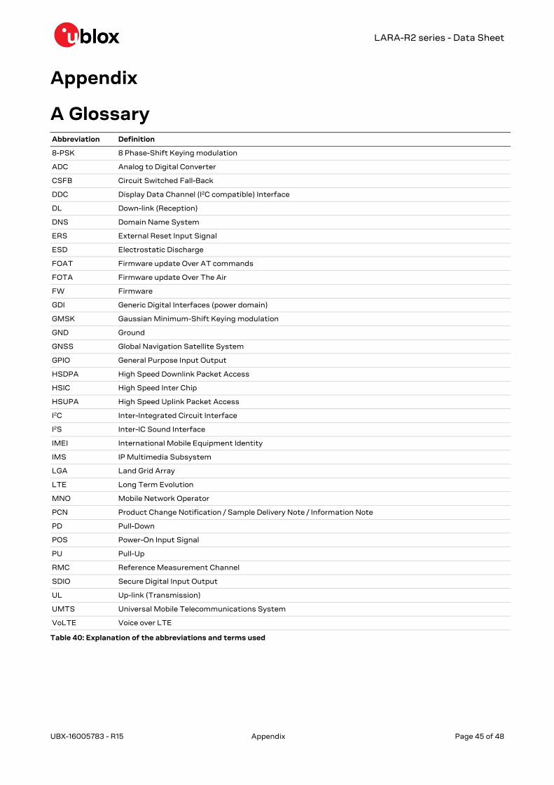
LARA-R2 series - Data Sheet
UBX-16005783 - R15 Appendix Page 45 of 48
Appendix
A Glossary Abbreviation Definition
8-PSK 8 Phase-Shift Keying modulation
ADC Analog to Digital Converter
CSFB Circuit Switched Fall-Back
DDC Display Data Channel (I2C compatible) Interface
DL Down-link (Reception)
DNS Domain Name System
ERS External Reset Input Signal
ESD Electrostatic Discharge
FOAT Firmware update Over AT commands
FOTA Firmware update Over The Air
FW Firmware
GDI Generic Digital Interfaces (power domain)
GMSK Gaussian Minimum-Shift Keying modulation
GND Ground
GNSS Global Navigation Satellite System
GPIO General Purpose Input Output
HSDPA High Speed Downlink Packet Access
HSIC High Speed Inter Chip
HSUPA High Speed Uplink Packet Access
I2C Inter-Integrated Circuit Interface
I2S Inter-IC Sound Interface
IMEI International Mobile Equipment Identity
IMS IP Multimedia Subsystem
LGA Land Grid Array
LTE Long Term Evolution
MNO Mobile Network Operator
PCN Product Change Notification / Sample Delivery Note / Information Note
PD Pull-Down
POS Power-On Input Signal
PU Pull-Up
RMC Reference Measurement Channel
SDIO Secure Digital Input Output
UL Up-link (Transmission)
UMTS Universal Mobile Telecommunications System
VoLTE Voice over LTE
Table 40: Explanation of the abbreviations and terms used
LARA-R2 series - Data Sheet
UBX-16005783 - R15 Related documents Page 46 of 48
Related documents [1] u-blox AT Commands Manual, Doc. No. UBX-13002752
[2] u-blox LARA-R2 series System Integration Manual, Doc. No. UBX-16010573
[3] u-blox Android RIL Production delivery Application note, Doc. No. UBX-13002041
[4] u-blox GNSS Implementation Application Note, Doc. No. UBX-13001849
[5] u-blox Mux Implementation Application Note, Doc. No. UBX-13001887
[6] u-blox Package Information User Guide, Doc. No. UBX-14001652
[7] 3GPP TS 27.007 - AT command set for User Equipment (UE)
[8] 3GPP TS 27.005 - Use of Data Terminal Equipment - Data Circuit terminating Equipment (DTE
- DCE) interface for Short Message Service (SMS) and Cell Broadcast Service (CBS)
[9] 3GPP TS 27.010 - Terminal Equipment to User Equipment (TE-UE) multiplexer protocol
[10] 3GPP TS 26.267 - Technical Specification Group Services and System Aspects; eCall Data
Transfer; In-band modem solution; General description
[11] 3GPP TS 36.521-1 - Evolved Universal Terrestrial Radio Access; User Equipment conformance
specification; Radio transmission and reception; Part 1: Conformance Testing
[12] 3GPP TS 34.121-1 - User Equipment conformance specification; Radio transmission and
reception (FDD); Part 1: Conformance specification
[13] 3GPP TS 51.010-1 - Mobile Station conformance specification; Part 1: Conformance
specification
[14] ITU-T Recommendation V24, 02-2000. List of definitions for interchange circuits between
Data Terminal Equipment (DTE) and Data Connection Equipment (DCE)
[15] Universal Serial Bus Specification, Revision 2.0,
http://www.usb.org/developers/docs/usb20_docs/
[16] High-Speed Inter-Chip USB Specification, Version 1.0,
http://www.usb.org/developers/docs/usb20_docs/
[17] I2C-bus specification and user manual - Rev. 5 - 9 October 2012 - NXP Semiconductors,
http://www.nxp.com/documents/user_manual/UM10204.pdf
☞ For regular updates to u-blox documentation and to receive product change notifications, register
on our homepage (www.u-blox.com).
LARA-R2 series - Data Sheet
UBX-16005783 - R15 Revision history Page 47 of 48
Revision history Revision Date Name Comments
R01 03-Mar-2016 sses Initial release
R02 31-May-2016 sses Document applicability updated to LARA-R204 and LARA-R211.
Improved description of VCC, Power-on, Reset, Host select, UART, USB, HSIC,
GPIO pins
R03 15-Jul-2016 sses Added description of reels and tapes.
Added current consumption and RF performance figures.
Updated description of Power-on, Reset, UART, USB pins.
R04 11-Oct-2016 sses Updated audio support.
Updated PWR_ON, ANT_DET, GPIO and Clock Output description.
Added 2G current consumption figures and remark in mechanical.
R05 25-Nov-2016 sses Updated Power-on and Power-off sections.
R06 20-Dec-2016 sses "Disclosure restriction" replaces "Document status" on page 2 and document
footer
Extended the document applicability to LARA-R203-02B
R07 17-Mar-2017 sses Updated GPRS / EDGE multi-slot class.
Added AC characteristics of I2S pins and other minor characteristics.
Updated VUSB_DET pin logical levels input ranges.
Extended the document applicability to LARA-R202-02B
R08 19-Apr-2017 sses Updated extended VCC range of LARA-R211 modules.
Updated LARA-R204-02B and LARA-R211-02B product status.
R09 29-May-2017 sses Updated LARA-R203-02B product status to Engineering Sample.
R10 30-Jun-2017 sses Updated LARA-R202-02B product status.
Extended the document applicability to LARA-R220 and LARA-R280.
R11 16-Aug-2017 sses Updated LARA-R203-02B, LARA-R220-62B and LARA-R280-02B product
status.
R12 22-Sep-2017 sses Updated LARA-R202-02B product status.
R13 27-Oct-2017 sses Updated LARA-R202-02B, LARA-R220-62B and LARA-R280-02B product
status.
R14 15-Dec-2017 lpah Updated LARA-R280-02B product status.
R15 27-May-2018 lpah Extended document applicability to LARA-R202-02B-01, LARA-R203-02B-01,
LARA-R204-02B-01 and LARA-R280-02B-01
LARA-R2 series - Data Sheet
UBX-16005783 - R15 Contact Page 48 of 48
Contact For complete contact information, visit us at www.u-blox.com.
u-blox Offices
North, Central and South America
u-blox America, Inc.
Phone: +1 703 483 3180
E-mail: [email protected]
Regional Office West Coast:
Phone: +1 408 573 3640
E-mail: [email protected]
Technical Support:
Phone: +1 703 483 3185
E-mail: [email protected]
Headquarters
Europe, Middle East, Africa
u-blox AG
Phone: +41 44 722 74 44
E-mail: [email protected]
Support: [email protected]
Asia, Australia, Pacific
u-blox Singapore Pte. Ltd.
Phone: +65 6734 3811
E-mail: [email protected]
Support: [email protected]
Regional Office Australia:
Phone: +61 2 8448 2016
E-mail: [email protected]
Support: [email protected]
Regional Office China (Beijing):
Phone: +86 10 68 133 545
E-mail: [email protected]
Support: [email protected]
Regional Office China (Chongqing):
Phone: +86 23 6815 1588
E-mail: [email protected]
Support: [email protected]
Regional Office China (Shanghai):
Phone: +86 21 6090 4832
E-mail: [email protected]
Support: [email protected]
Regional Office China (Shenzhen):
Phone: +86 755 8627 1083
E-mail: [email protected]
Support: [email protected]
Regional Office India:
Phone: +91 80 405 092 00
E-mail: [email protected]
Support: [email protected]
Regional Office Japan (Osaka):
Phone: +81 6 6941 3660
E-mail: [email protected]
Support: [email protected]
Regional Office Japan (Tokyo):
Phone: +81 3 5775 3850
E-mail: [email protected]
Support: [email protected]
Regional Office Korea:
Phone: +82 2 542 0861
E-mail: [email protected]
Support: [email protected]
Regional Office Taiwan:
Phone: +886 2 2657 1090
E-mail: [email protected]
Support: [email protected]
Recommended