IS31FL3731
Integrated Silicon Solution, Inc. – www.issi.com 1 Rev.D, 04/22/2013
AUDIO MODULATED MATRIX LED DRIVER
May 2013
GENERAL DESCRIPTION
The IS31FL3731 is a compact LED driver for 144 single LEDs. The device can be programmed via an I2C compatible interface. The IS31FL3731 offers two blocks each driving 72 LEDs with 1/9 cycle rate. The required lines to drive all 144 LEDs are reduced to 18 by using the cross-plexing feature optimizing space on the PCB. Additionally each of the 144 LEDs can be dimmed individually with 8-bit allowing 256 steps of linear dimming.
To reduce CPU usage up to 8 frames can be stored with individual time delays between frames to play small animations automatically. LED frames can be modulated with audio signal.
IS31FL3731 is available in QFN-28 (4mm × 4mm) and SSOP-28 package. It operates from 2.7V to 5.5V over the temperature range of -40°C to +85°C.
FEATURES
Supply voltage range: 2.7V to 5.5V 400kHz I2C-compatible interface 144 LEDs in dot matrix Individual blink control 8 frames memory for animations Picture mode and animation mode Auto intensity breathing during the switching of
different frames LED frames displayed can be modulated with
audio signal intensity LED light intensity can be modulated with audio
signal intensity QFN-28 (4mm × 4mm) and SSOP-28 package
APPLICATIONS
Mobile phones and other hand-held devices for LED display
LED in home appliances
TYPICAL APPLICATION CIRCUIT
Figure 1 Typical Application Circuit
Note 1: The IC should be placed far away from the mobile antenna in order to prevent the EMI.
Note 2: The average current of each LED is 3.2mA when REXT = 20kΩ. The LED current can be modulated by the REXT. Please refer to the detail information in Page 18.
IS31FL3731
Integrated Silicon Solution, Inc. – www.issi.com 2 Rev.D, 04/22/2013
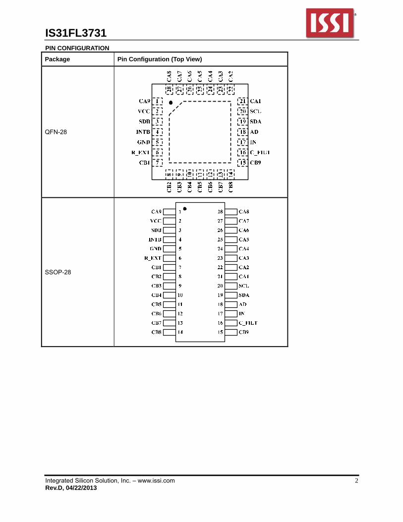
PIN CONFIGURATION
Package Pin Configuration (Top View)
QFN-28
SSOP-28

IS31FL3731
Integrated Silicon Solution, Inc. – www.issi.com 3 Rev.D, 04/22/2013
PIN DESCRIPTION
No. Pin Description
1 CA9 LED matrix A current output/input port.
2 VCC Power supply.
3 SDB Shutdown the chip when pull to low.
4 INTB Interrupt output. Active low.
5 GND Ground.
6 R_EXT 20kΩ resistance to confirm the LED current.
7 ~ 15 CB1 ~ CB9 LED matrix B current output/input port.
16 C_FILT Capacitor used for audio.
17 IN Audio input.
18 AD I2C address setting.
19 SDA I2C compatible serial data.
20 SCL I2C compatible serial clock.
21 ~ 28 CA1 ~ CA8 LED matrix A current output/input port.
Thermal Pad Connect to GND.
Copyright © 2013 Integrated Silicon Solution, Inc. All rights reserved. ISSI reserves the right to make changes to this specification and its products at any time without notice. ISSI assumes no liability arising out of the application or use of any information, products or services described herein. Customers are advised to obtain the latest version of this device specification before relying on any published information and before placing orders for products. Integrated Silicon Solution, Inc. does not recommend the use of any of its products in life support applications where the failure or malfunction of the product can reasonably be expected to cause failure of the life support system or to significantly affect its safety or effectiveness. Products are not authorized for use in such applications unless Integrated Silicon Solution, Inc. receives written assurance to its satisfaction, that: a.) the risk of injury or damage has been minimized; b.) the user assume all such risks; and c.) potential liability of Integrated Silicon Solution, Inc is adequately protected under the circumstances
IS31FL3731
Integrated Silicon Solution, Inc. – www.issi.com 4 Rev.D, 04/22/2013
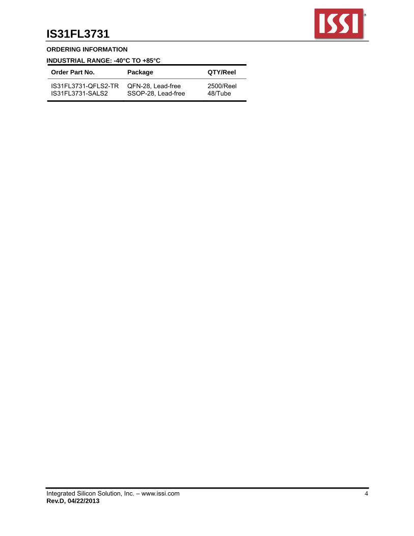
ORDERING INFORMATION
INDUSTRIAL RANGE: -40°C TO +85°C
Order Part No. Package QTY/Reel
IS31FL3731-QFLS2-TR IS31FL3731-SALS2
QFN-28, Lead-free SSOP-28, Lead-free
2500/Reel 48/Tube
IS31FL3731
Integrated Silicon Solution, Inc. – www.issi.com 5 Rev.D, 04/22/2013
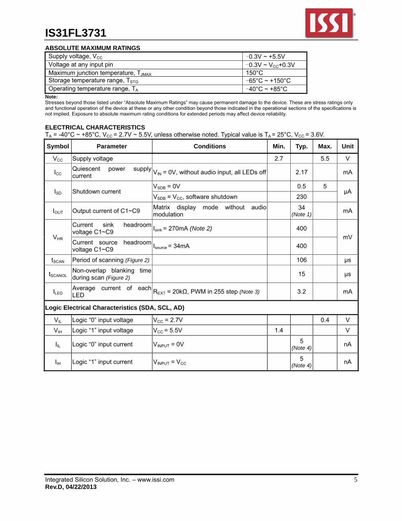
ABSOLUTE MAXIMUM RATINGS Supply voltage, VCC -0.3V ~ +5.5V Voltage at any input pin -0.3V ~ VCC+0.3V Maximum junction temperature, TJMAX 150°C Storage temperature range, TSTG -65°C ~ +150°C Operating temperature range, TA -40°C ~ +85°C
Note: Stresses beyond those listed under “Absolute Maximum Ratings” may cause permanent damage to the device. These are stress ratings only and functional operation of the device at these or any other condition beyond those indicated in the operational sections of the specifications is not implied. Exposure to absolute maximum rating conditions for extended periods may affect device reliability. ELECTRICAL CHARACTERISTICS TA = -40°C ~ +85°C, VCC = 2.7V ~ 5.5V, unless otherwise noted. Typical value is TA = 25°C, VCC = 3.6V.
Symbol Parameter Conditions Min. Typ. Max. Unit
VCC Supply voltage 2.7 5.5 V
ICC Quiescent power supply current
VIN = 0V, without audio input, all LEDs off 2.17 mA
ISD Shutdown current VSDB = 0V 0.5 5
μA VSDB = VCC, software shutdown 230
IOUT Output current of C1~C9 Matrix display mode without audio modulation
34 (Note 1)
mA
VHR
Current sink headroom voltage C1~C9
Isink = 270mA (Note 2) 400
mV Current source headroom voltage C1~C9
Isource = 34mA 400
tSCAN Period of scanning (Figure 2) 106 µs
tSCANOL Non-overlap blanking time during scan (Figure 2)
15 µs
ILED Average current of each LED
REXT = 20kΩ, PWM in 255 step (Note 3) 3.2 mA
Logic Electrical Characteristics (SDA, SCL, AD)
VIL Logic “0” input voltage VCC = 2.7V 0.4 V
VIH Logic “1” input voltage VCC = 5.5V 1.4 V
IIL Logic “0” input current VINPUT = 0V 5 (Note 4)
nA
IIH Logic “1” input current VINPUT = VCC 5 (Note 4)
nA

IS31FL3731
Integrated Silicon Solution, Inc. – www.issi.com 6 Rev.D, 04/22/2013
DIGITAL INPUT SWITCHING CHARACTERISTICS (Note 4)
Symbol Parameter Condition Min. Typ. Max. Units
fSCL Serial-Clock frequency 400 kHz
tBUF Bus free time between a STOP and a START condition
1.3 μs
tHD, STA Hold time (repeated) START condition 0.6 μs
tSU, STA Repeated START condition setup time 0.6 μs
tSU, STO STOP condition setup time 0.6 μs
tHD, DAT Data hold time 0.9 μs
tSU, DAT Data setup time 100 ns
tLOW SCL clock low period 1.3 μs
tHIGH SCL clock high period 0.7 μs
tR Rise time of both SDA and SCL signals, receiving
(Note 5) 20+0.1Cb 300 ns
tF Fall time of both SDA and SCL signals, receiving (Note 5) 20+0.1Cb 300 ns
Note 1: The average current of each LED is IOUT/10.5.
Note 2: All LEDs are on.
Note 3: ILED = 64.7/REXT, REXT = 20kΩ is recommended. The recommended minimum value of REXT is 18kΩ, or it may cause a large current.
Note 4: Guaranteed by design.
Note 5: Cb = total capacitance of one bus line in pF. ISINK ≤ 6mA. tR and tF measured between 0.3 × VCC and 0.7 × VCC.
Figure 2 Scanning timing
IS31FL3731
Integrated Silicon Solution, Inc. – www.issi.com 7 Rev.D, 04/22/2013
DETAILED DESCRIPTION
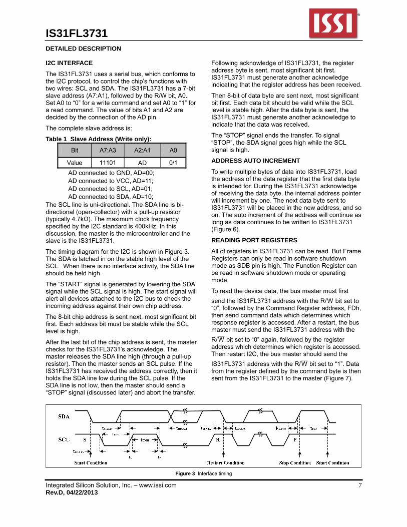
I2C INTERFACE
The IS31FL3731 uses a serial bus, which conforms to the I2C protocol, to control the chip’s functions with two wires: SCL and SDA. The IS31FL3731 has a 7-bit slave address (A7:A1), followed by the R/W bit, A0. Set A0 to “0” for a write command and set A0 to “1” for a read command. The value of bits A1 and A2 are decided by the connection of the AD pin.
The complete slave address is:
Table 1 Slave Address (Write only):
Bit A7:A3 A2:A1 A0
Value 11101 AD 0/1
AD connected to GND, AD=00; AD connected to VCC, AD=11; AD connected to SCL, AD=01; AD connected to SDA, AD=10; The SCL line is uni-directional. The SDA line is bi-directional (open-collector) with a pull-up resistor (typically 4.7kΩ). The maximum clock frequency specified by the I2C standard is 400kHz. In this discussion, the master is the microcontroller and the slave is the IS31FL3731.
The timing diagram for the I2C is shown in Figure 3. The SDA is latched in on the stable high level of the SCL. When there is no interface activity, the SDA line should be held high.
The “START” signal is generated by lowering the SDA signal while the SCL signal is high. The start signal will alert all devices attached to the I2C bus to check the incoming address against their own chip address.
The 8-bit chip address is sent next, most significant bit first. Each address bit must be stable while the SCL level is high.
After the last bit of the chip address is sent, the master checks for the IS31FL3731’s acknowledge. The master releases the SDA line high (through a pull-up resistor). Then the master sends an SCL pulse. If the IS31FL3731 has received the address correctly, then it holds the SDA line low during the SCL pulse. If the SDA line is not low, then the master should send a “STOP” signal (discussed later) and abort the transfer.
Following acknowledge of IS31FL3731, the register address byte is sent, most significant bit first. IS31FL3731 must generate another acknowledge indicating that the register address has been received.
Then 8-bit of data byte are sent next, most significant bit first. Each data bit should be valid while the SCL level is stable high. After the data byte is sent, the IS31FL3731 must generate another acknowledge to indicate that the data was received.
The “STOP” signal ends the transfer. To signal “STOP”, the SDA signal goes high while the SCL signal is high.
ADDRESS AUTO INCREMENT
To write multiple bytes of data into IS31FL3731, load the address of the data register that the first data byte is intended for. During the IS31FL3731 acknowledge of receiving the data byte, the internal address pointer will increment by one. The next data byte sent to IS31FL3731 will be placed in the new address, and so on. The auto increment of the address will continue as long as data continues to be written to IS31FL3731 (Figure 6).
READING PORT REGISTERS
All of registers in IS31FL3731 can be read. But Frame Registers can only be read in software shutdown mode as SDB pin is high. The Function Register can be read in software shutdown mode or operating mode.
To read the device data, the bus master must first
send the IS31FL3731 address with the R/W____
bit set to “0”, followed by the Command Register address, FDh, then send command data which determines which response register is accessed. After a restart, the bus master must send the IS31FL3731 address with the
R/W____
bit set to “0” again, followed by the register address which determines which register is accessed. Then restart I2C, the bus master should send the
IS31FL3731 address with the R/W____
bit set to “1”. Data from the register defined by the command byte is then sent from the IS31FL3731 to the master (Figure 7).
Figure 3 Interface timing

IS31FL3731
Integrated Silicon Solution, Inc. – www.issi.com 8 Rev.D, 04/22/2013
Figure 4 Bit transfer
Figure 5 Writing to IS31FL3731(Typical)
Figure 6 Writing to IS31FL3731(Automatic address increment)
Figure 7 Reading from IS31FL3731

IS31FL3731
Integrated Silicon Solution, Inc. – www.issi.com 9 Rev.D, 04/22/2013
REGISTER DEFINITION Table 2 FDh Command Register
Data Function Data Function
0000 0000 Point to Page One(Frame 1 Register is available) 0000 0001 Point to Page Two(Frame 2 Register is available)
0000 0010 Point to Page Three(Frame 3 Register is available) 0000 0011 Point to Page Four(Frame 4 Register is available)
0000 0100 Point to Page Five(Frame 5 Register is available) 0000 0101 Point to Page Six(Frame 6 Register is available)
0000 0110 Point to Page Seven(Frame 7 Register is available) 0000 0111 Point to Page Eight(Frame 8 Register is available)
0000 1011 Point to Page Nine(Function Register is available) Others Reserved
Note: The Command Register should be configured first after writing in the slave address to choose the available register (Frame Registers and Function Registers). Then write data in the choosing register. For example, when write “0000 0011” in the Command Register (FDh), the data which writing after will be stored in the Frame 4 Register. Write new data can configure other registers.
Table 3 Response Register Function (The address of each Page is starting from 00h. Frame Registers have the same format.)
Address Name Function Table R/W Default
Frame Register (Page One to Page Eight) (Note 6)
00h ~ 11h LED Control Register Store on or off state for each LED 4 R/W
xxxx xxxx
12h ~ 23h Blink Control Register Control the blink function for each LED 5 R/W
24h ~ B3h PWM Register 144 LEDs PWM duty cycle data register
6 R/W
Function Register (Page Night)
00h Configuration Register Configure the operation mode 8 R/W
0000 0000
01h Picture Display Register Set the display frame in Picture Mode 9 R/W
02h Auto Play Control Register 1 Set the way of display in Auto Frame Play Mode
10 R/W
03h Auto Play Control Register 2 Set the delay time in Auto Frame Play Mode
11 R/W
04h Reserved (Note 7) Reserved - R/W
05h Display Option Register Set the display option 12 R/W
06h Audio Synchronization Register
Set audio synchronization function 13 R/W
07h Frame State Register Store the frame display information 14 R
08h Breath Control Register 1 Set fade in and fade out time for breath function
15 R/W
09h Breath Control Register 2 Set the breath function 16 R/W
0Ah Shutdown Register Set software shutdown mode 17 R/W
0Bh AGC Control Register Set the AGC function and the audio gain.
18 R/W
0Ch Audio ADC Rate Register Set the ADC sample rate of the input signal
19 R/W
Note 6: The data of Frame Registers is not assured when power on. Please initialize the Frame Registers first to ensure operate normally.
Note 7: The 04h register has no function although it can be written. It also can be read but the data is not assured.
IS31FL3731
Integrated Silicon Solution, Inc. – www.issi.com 10 Rev.D, 04/22/2013
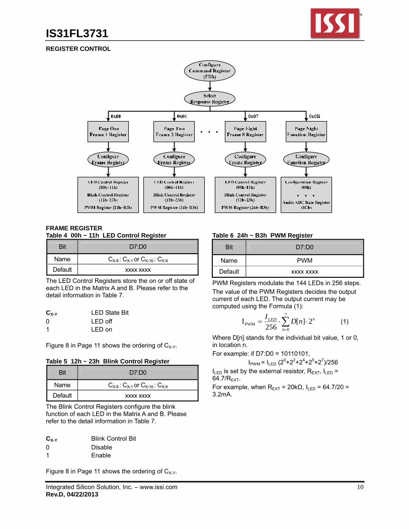
REGISTER CONTROL
FRAME REGISTER Table 4 00h ~ 11h LED Control Register
Bit D7:D0
Name CX-8 : CX-1 or CX-16 : CX-9
Default xxxx xxxx
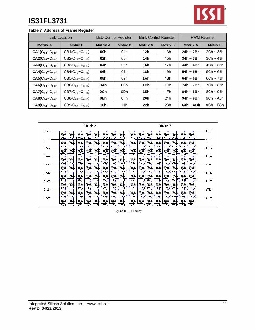
The LED Control Registers store the on or off state of each LED in the Matrix A and B. Please refer to the detail information in Table 7. CX-Y LED State Bit 0 LED off 1 LED on Figure 8 in Page 11 shows the ordering of CX-Y. Table 5 12h ~ 23h Blink Control Register
Bit D7:D0
Name CX-8 : CX-1 or CX-16 : CX-9
Default xxxx xxxx
The Blink Control Registers configure the blink function of each LED in the Matrix A and B. Please refer to the detail information in Table 7. CX-Y Blink Control Bit 0 Disable 1 Enable Figure 8 in Page 11 shows the ordering of CX-Y.
Table 6 24h ~ B3h PWM Register
Bit D7:D0
Name PWM
Default xxxx xxxx
PWM Registers modulate the 144 LEDs in 256 steps. The value of the PWM Registers decides the output current of each LED. The output current may be computed using the Formula (1):
7
0PWM 2][
256I
n
nLED nDI
(1)
Where D[n] stands for the individual bit value, 1 or 0, in location n. For example: if D7:D0 = 10110101,
IPWM = ILED (20+22+24+25+27)/256 ILED is set by the external resistor, REXT, ILED = 64.7/REXT. For example, when REXT = 20kΩ, ILED = 64.7/20 = 3.2mA.
IS31FL3731
Integrated Silicon Solution, Inc. – www.issi.com 11 Rev.D, 04/22/2013
Table 7 Address of Frame Register
LED Location LED Control Register Blink Control Register PWM Register
Matrix A Matrix B Matrix A Matrix B Matrix A Matrix B Matrix A Matrix B
CA1(C1-1~C1-8) CB1(C1-9~C1-16) 00h 01h 12h 13h 24h ~ 2Bh 2Ch ~ 33h
CA2(C2-1~C2-8) CB2(C2-9~C2-16) 02h 03h 14h 15h 34h ~ 3Bh 3Ch ~ 43h
CA3(C3-1~C3-8) CB3(C3-9~C3-16) 04h 05h 16h 17h 44h ~ 4Bh 4Ch ~ 53h
CA4(C4-1~C4-8) CB4(C4-9~C4-16) 06h 07h 18h 19h 54h ~ 5Bh 5Ch ~ 63h
CA5(C5-1~C5-8) CB5(C5-9~C5-16) 08h 09h 1Ah 1Bh 64h ~ 6Bh 6Ch ~ 73h
CA6(C6-1~C6-8) CB6(C6-9~C6-16) 0Ah 0Bh 1Ch 1Dh 74h ~ 7Bh 7Ch ~ 83h
CA7(C7-1~C7-8) CB7(C7-9~C7-16) 0Ch 0Dh 1Eh 1Fh 84h ~ 8Bh 8Ch ~ 93h
CA8(C8-1~C8-8) CB8(C8-9~C8-16) 0Eh 0Fh 20h 21h 94h ~ 9Bh 9Ch ~ A3h
CA9(C9-1~C9-8) CB9(C9-9~C9-16) 10h 11h 22h 23h A4h ~ ABh ACh ~ B3h
Figure 8 LED array

IS31FL3731
Integrated Silicon Solution, Inc. – www.issi.com 12 Rev.D, 04/22/2013
FUNCTION REGISTER Table 8 00h Configuration Register
Bit D7:D5 D4:D3 D2:D0
Name - MODE FS
Default 000 00 000
The Configuration Register sets operating mode of IS31FL3731. MODE Display Mode 00 Picture Mode 01 Auto Frame Play Mode 1x Audio Frame Play Mode FS Frame Start (Available in Auto Frame Play Mode) 000 Frame 1 001 Frame 2 010 Frame 3 011 Frame 4 100 Frame 5 101 Frame 6 110 Frame 7 111 Frame 8 FS bit sets the start frame in Auto Frame Play Mode. Movie starts from Frame 4 when the FS bit is set to “011”. The FS bit is only available in Auto Frame Play Mode. Table 9 01h Picture Display Register
Bit D7:D3 D2:D0
Name - PFS
Default 00000 000
The Picture Display Register sets display frame in Picture Mode. PFS Picture Frame Selection (Available in Picture Mode) 000 Frame 1 001 Frame 2 010 Frame 3 011 Frame 4 100 Frame 5 101 Frame 6 110 Frame 7 111 Frame 8
Table 10 02h Auto Play Control Register 1
Bit D7 D6:D4 D3 D2:D0
Name - CNS - FNS
Default 0 000 0 000
The Auto Play Control Register 1 sets the way of display in Auto Frame Play Mode. CNS Number of Loops Playing Selection (Available in Auto Frame Play Mode) 000 Play endless 001 1 loop 010 2 loops 011 3 loops 100 4 loops 101 5 loops 110 6 loops 111 7 loops
FNS Number of Frames Playing Selection (Available in Auto Frame Play Mode) 000 All Frame 001 1 frame 010 2 frames 011 3 frames 100 4 frames 101 5 frames 110 6 frames 111 7 frames Movie will be stop in the next frame of the cycle. For example, FS bit is set to “011”, CNS bit is set to “011” and FNS bit is set to “011”. Then the movie will play from frame 4 to frame 6 and play three times it stops in frame 7.
Table 11 03h Auto Play Control Register 2
Bit D7:D6 D5:D0
Name - A
Default 00 000000
The Auto Play Control Register 2 sets the delay time in Auto Frame Play Mode (Figure 12). FDT Frame Delay Time (Available in Auto Frame Play Mode) If A = 0, FDT = τ×64; If A = 1~63, FDT = τ×A; A = 0~63 and τ = 11ms (Typ.); For example, when A = 23, FDT is 11ms×23 = 253ms

IS31FL3731
Integrated Silicon Solution, Inc. – www.issi.com 13 Rev.D, 04/22/2013
Table 12 05h Display Option Register
Bit D7:D6 D5 D4 D3 D2:D0
Name - IC - BE A
Default 00 0 0 0 000
The Display Option Register sets display option of IS31FL3731. IC Intensity Control 0 Set the intensity of each frame
independently 1 Use intensity setting of frame 1 for all
other frames BE Blink Enable 0 Disable 1 Enable BPT Blink Period Time BPT = τ×A; A = 0~7, τ = 0.27s (Typ.); For example, when A = 5, BPT is 0.27s×5 = 1.35s. The duty cycle for blink function is 50%. Table 13 06h Audio Synchronization Register
Bit D7:D1 D0
Name - AE
Default 0000000 0
The Audio Synchronization Register sets audio synchronization function. AE Audio Synchronization Enable 0 Audio synchronization disable 1 Enable audio signal to modulate the intensity of the matrix The intensity of matrix can be modulated by the audio input signal basing on each LED’s current is set by PWM when the AE bit is set to “1”.
Table 14 07h Frame State Register (Read Only)
Bit D7:D5 D4 D3 D2:D0
Name - INT - CFD
Default -
The Frame State Register stores the frame display information. INT Interrupt Bit (Available in Auto Frame Play Mode) 0 Movie does not finish 1 Movie has finished CFD Current Frame Display 000 Frame 1 001 Frame 2 010 Frame 3 011 Frame 4 100 Frame 5 101 Frame 6 110 Frame 7 111 Frame 8 The INT bit will be set to “1” automatically when movie is end in Auto Frame Play Mode. The INT bit can be cleared up by reading the Frame State Register. Table 15 08h Breath Control Register 1
Bit D7 D6:D4 D3 D2:D0
Name - A - B
Default 0 000 0 000
The Breath Control Register 1 sets fade in and fade out time for breath function. FOT Fade Out Time FOT = τ×2A A = 0~7, τ = 26ms (Typ.) For example, when A = 4, FOT is 26ms×24 = 416ms FIT Fade In Time FIT = τ×2B B = 0~7, τ = 26ms (Typ.) For example, when A = 4, FIT is 26ms×24 = 416ms
IS31FL3731
Integrated Silicon Solution, Inc. – www.issi.com 14 Rev.D, 04/22/2013
Table 16 09h Breath Control Register 2
Bit D7:D5 D4 D3 D2:D0
Name - B_EN - A
Default 000 0 0 000
The Breath Control Register 2 sets the breath function. B_EN Breath Enable
(Available in Picture Mode and Auto Frame Play Mode) 0 Disable 1 Enable ET Extinguish Time
ET = τ×2A A = 0~7, τ = 3.5ms (Typ.) For example, when A = 4, ET is 3.5ms×24 = 56ms Table 17 0Ah Shutdown Register
Bit D7:D1 D0
Name - SSD
Default 0000000 0
The Shutdown Register sets software shutdown mode. SSD Shutdown Control 0 Shutdown Mode 1 Normal Operation Table 18 0Bh AGC Control Register
Bit D7:D5 D4 D3 D2:D0
Name - AGCM AGC AGS
Default 000 0 0 000
The AGC Control Register sets the AGC function and the audio gain. AGCM AGC Mode 0 Slow Mode 1 Fast Mode AGC AGC Enable 0 Disable 1 Enable
AGS Audio Gain Selection 000 0dB 001 3dB 010 6dB 011 9dB 100 12dB 101 15dB 110 18dB 111 21dB The AGS bit is available in Audio Frame Play Mode and audio synchronization mode. Table 19 0Ch Audio ADC Rate Register
Bit D7:D0
Name A
Default 0000 0000
The Audio ADC Rate Register sets the ADC sample rate of the input signal in Audio Frame Play Mode. AAR Audio ADC Rate (Available in Audio Frame Play Mode) If A = 0, AAR = τ×256 If A = 1~255, AAR = τ×A τ = 46μs (Typ.) For example, when A = 14, AAR is 46μs×14 = 644μs
IS31FL3731
Integrated Silicon Solution, Inc. – www.issi.com 15 Rev.D, 04/22/2013
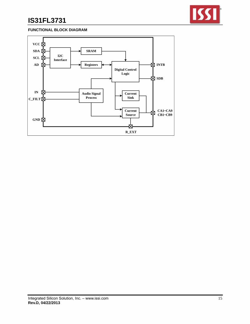
FUNCTIONAL BLOCK DIAGRAM
SDA
SCLI2C
Interface
Registers
Digital Control Logic
Current Source
SRAM
VCC
GND
Current Sink
AD
CA1~CA9CB1~CB9
R_EXT
SDB
INTB
Audio SignalProcess
IN
C_FILT

IS31FL3731
Integrated Silicon Solution, Inc. – www.issi.com 16 Rev.D, 04/22/2013
APPLICATION INFORMATION (The description below is for the Function Register unless otherwise noted.) PWM CONTROL
The brightness of 144 LEDs can be modulated with 256 steps by PWM Register. For example, if the data in PWM Register is “0000 0100”, then the PWM is the fourth step.
Writing new data continuously to the registers can modulate the brightness of the LEDs to achieve a breathing effect.
GAMMA CORRECTION
In order to perform a better visual LED breathing effect we recommend using a gamma corrected PWM value to set the LED intensity. This results in a reduced number of steps for the LED intensity setting, but causes the change in intensity to appear more linear to the human eye.
Gamma correction, also known as gamma compression or encoding, is used to encode linear luminance to match the non-linear characteristics of display. Since the IS31FL3731 can modulate the brightness of the LEDs with 256 steps, a gamma correction function can be applied when computing each subsequent LED intensity setting such that the changes in brightness matches the human eye's brightness curve.
Table 17 32 gamma steps with 256 PWM steps
C(0) C(1) C(2) C(3) C(4) C(5) C(6) C(7)
0 1 2 4 6 10 13 18
C(8) C(9) C(10) C(11) C(12) C(13) C(14) C(15)
22 28 33 39 46 53 61 69
C(16) C(17) C(18) C(19) C(20) C(21) C(22) C(23)
78 86 96 106 116 126 138 149
C(24) C(25) C(26) C(27) C(28) C(29) C(30) C(31)
161 173 186 199 212 226 240 255
0
32
64
96
128
160
192
224
256
0 4 8 12 16 20 24 28 32
PW
M D
ata
Intensity Steps Figure 9 Gamma Correction(32 Steps)
Choosing more gamma steps provides for a more continuous looking breathing effect. This is useful for very long breathing cycles. The recommended
configuration is defined by the breath cycle T. When T=1s, choose 32 gamma steps, when T=2s, choose 64 gamma steps. The user must decide the final number of gamma steps not only by the LED itself, but also based on the visual performance of the finished product.
Table 18 64 gamma steps with 256 PWM steps
C(0) C(1) C(2) C(3) C(4) C(5) C(6) C(7)
0 1 2 3 4 5 6 7
C(8) C(9) C(10) C(11) C(12) C(13) C(14) C(15)
8 10 12 14 16 18 20 22
C(16) C(17) C(18) C(19) C(20) C(21) C(22) C(23)
24 26 29 32 35 38 41 44
C(24) C(25) C(26) C(27) C(28) C(29) C(30) C(31)
47 50 53 57 61 65 69 73
C(32) C(33) C(34) C(35) C(36) C(37) C(38) C(39)
77 81 85 89 94 99 104 109
C(40) C(41) C(42) C(43) C(44) C(45) C(46) C(47)
114 119 124 129 134 140 146 152
C(48) C(49) C(50) C(51) C(52) C(53) C(54) C(55)
158 164 170 176 182 188 195 202
C(56) C(57) C(58) C(59) C(60) C(61) C(62) C(63)
209 216 223 230 237 244 251 255
0
32
64
96
128
160
192
224
256
0 8 16 24 32 40 48 56 64
PW
M D
ata
Intensity Steps Figure 10 Gamma Correction(64 Steps)
Note: The data of 32 gamma steps is the standard value and the data of 64 gamma steps is the recommended value.
OPERATING MODE
IS31FL3731 has three operating modes, Picture Mode, Auto Frame Play Mode and Audio Frame Play Mode.
PICTURE MODE
By setting the MODE bit of the Configuration Register (00h) to “00”, the IS31FL3731 operates in Picture Mode. Set the PFS bit of Picture Display Register (01h) to choose the display frame. The Picture Mode
IS31FL3731
Integrated Silicon Solution, Inc. – www.issi.com 17 Rev.D, 04/22/2013
can be operating with breath function by configuring Breath Control Register 2 (09h).
AUTO FRAME PLAY MODE
By setting the MODE bit of the Configuration Register (00h) to “01”, the IS31FL3731 operates in Auto Frame Play Mode. It stores data of 8 frames and automatically plays in order. Customers can configure the delay time between each two frames and the first playing frame by setting the FS bit of Configuration Register (00h). The Auto Play Control Register 1 (02h) can configure the display cycle and display frames.
Configure the Auto Play Control Register 2 (03h), Breath Control Register 1 (08h) and Breath Control Register 2 (09h) can set the breath time between two frames switching.
AUDIO FRAME PLAY MODE
By setting the MODE bit of the Configuration Register (00h) to “1x”, the IS31FL3731 operates in Audio Frame Play Mode. It stores data of 8 frames and the 8 frames playing follow the input signal. 0Ch register is used to set the ADC sample rate for the input signal to control frames playing. It plays the first frame when the value is the smallest and plays the eighth frame when the value is the biggest.
AUDIO MODULATED AND GAIN SETTING
By setting the AE bit of the Audio Synchronization Register (06h) to “1”, IS31FL3731 operates with audio synchronization. The intensity of LEDs is adjusted by the input signal. The audio input gain can be set by the AGC Control Register (0Bh).
BLINK FUNCTION SETTING
By setting the BE bit of the Display Option Register (05h) to “1”, blink function enable. If the BE bit is set to “1”, each LED can be controlled by the Blink Control Registers (12h~23h in Page One to Page Eight). The Display Option Register (05h) is used to set the blink period time, BPT, and the duty cycle is 50% (Figure 11).
Figure 11 Blink function
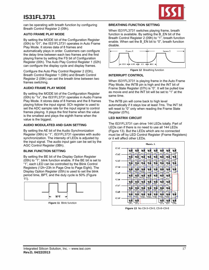
BREATHING FUNCTION SETTING
When IS31FL3731 switches playing frame, breath function is available. By setting the B_EN bit of the Breath Control Register 2 (09h) to “1”, breath function enable. When set the B_EN bit to “0”, breath function disable.
Figure 12 Breathing function
INTERRUPT CONTROL
When IS31FL3731 is playing frame in the Auto Frame Play Mode, the INTB pin is high and the INT bit of Frame State Register (07h) is “0”. It will be pulled low as movie end and the INT bit will be set to “1” at the same time.
The INTB pin will come back to high level automatically if it stays low at least 7ms. The INT bit will reset to “0” only when reading the Frame State Register (07h).
LED MATRIX CIRCUIT
The IS31FL3731 can drive 144 LEDs totally. Part of LEDs can if there is no need to use all 144 LEDs (Figure 13). But the LEDs which are no connected must be off by LED Control Register (Frame Registers) or it will affect other LEDs.
Figure 13 No C9-3~C9-5, C5-8~C9-8
IS31FL3731
Integrated Silicon Solution, Inc. – www.issi.com 18 Rev.D, 04/22/2013
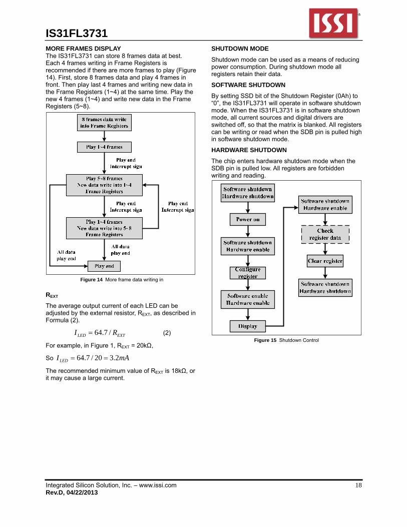
MORE FRAMES DISPLAY The IS31FL3731 can store 8 frames data at best. Each 4 frames writing in Frame Registers is recommended if there are more frames to play (Figure 14). First, store 8 frames data and play 4 frames in front. Then play last 4 frames and writing new data in the Frame Registers (1~4) at the same time. Play the new 4 frames (1~4) and write new data in the Frame Registers (5~8).
Figure 14 More frame data writing in
REXT
The average output current of each LED can be adjusted by the external resistor, REXT, as described in Formula (2).
EXTLED RI /7.64 (2)
For example, in Figure 1, REXT = 20kΩ,
So mAILED 2.320/7.64
The recommended minimum value of REXT is 18kΩ, or it may cause a large current.
SHUTDOWN MODE
Shutdown mode can be used as a means of reducing power consumption. During shutdown mode all registers retain their data.
SOFTWARE SHUTDOWN
By setting SSD bit of the Shutdown Register (0Ah) to “0”, the IS31FL3731 will operate in software shutdown mode. When the IS31FL3731 is in software shutdown mode, all current sources and digital drivers are switched off, so that the matrix is blanked. All registers can be writing or read when the SDB pin is pulled high in software shutdown mode.
HARDWARE SHUTDOWN
The chip enters hardware shutdown mode when the SDB pin is pulled low. All registers are forbidden writing and reading.
Figure 15 Shutdown Control
IS31FL3731
Integrated Silicon Solution, Inc. – www.issi.com 19 Rev.D, 04/22/2013
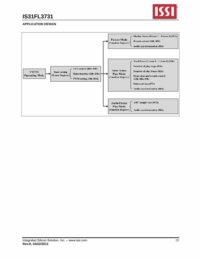
APPLICATION DESIGN
IS31FL3731
Integrated Silicon Solution, Inc. – www.issi.com 20 Rev.D, 04/22/2013
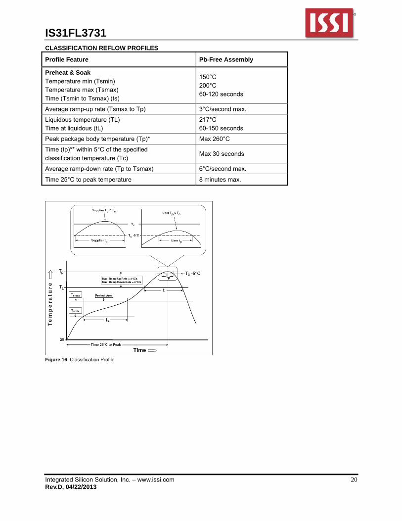
CLASSIFICATION REFLOW PROFILES
Profile Feature Pb-Free Assembly
Preheat & Soak Temperature min (Tsmin) Temperature max (Tsmax) Time (Tsmin to Tsmax) (ts)
150°C 200°C 60-120 seconds
Average ramp-up rate (Tsmax to Tp) 3°C/second max.
Liquidous temperature (TL) Time at liquidous (tL)
217°C 60-150 seconds
Peak package body temperature (Tp)* Max 260°C
Time (tp)** within 5°C of the specified classification temperature (Tc)
Max 30 seconds
Average ramp-down rate (Tp to Tsmax) 6°C/second max.
Time 25°C to peak temperature 8 minutes max.
Figure 16 Classification Profile
IS31FL3731
Integrated Silicon Solution, Inc. – www.issi.com 21 Rev.D, 04/22/2013
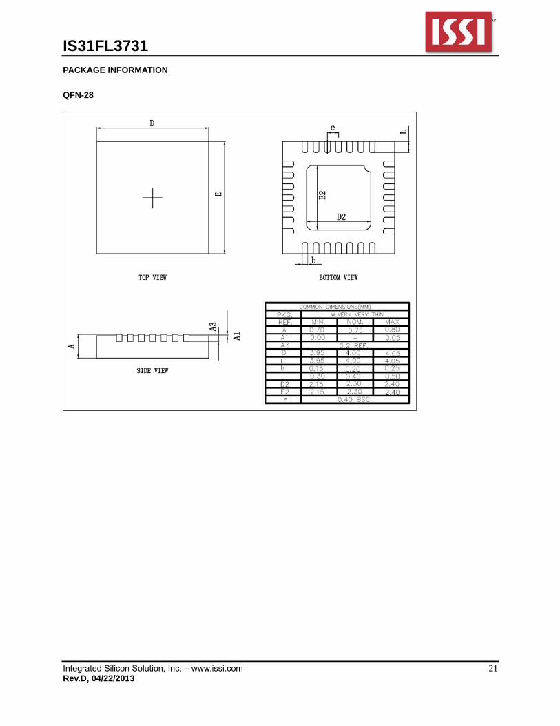
PACKAGE INFORMATION
QFN-28
IS31FL3731
Integrated Silicon Solution, Inc. – www.issi.com 22 Rev.D, 04/22/2013
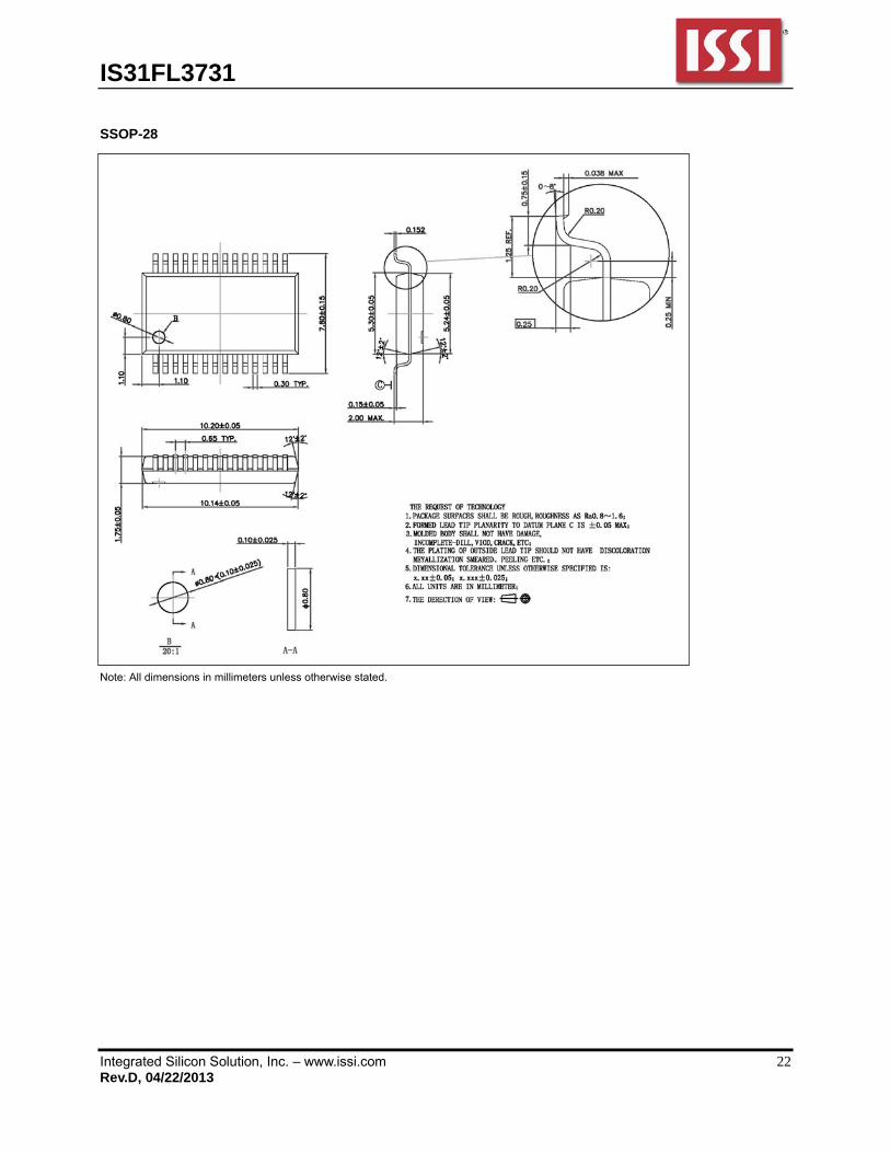
SSOP-28
Note: All dimensions in millimeters unless otherwise stated.
Recommended