6.152J / 3.155J SpringTerm 2005 Lecture 15 Handout -- Interconnects
Interconnects 1
6.152J / 3.155J Fall Term 2005 Lecture 15 -- Interconnects 1
Interconnects
Reading: Plummer, Chapter 11 – Backend TechnologyReferences: Campbell, Sections 11.9, 13.8, 15.6 - 15.10
1. Overview of Metallization2. Introduction to Deposition Methods3. Interconnect Technology4. Contact Technology5. Refractory Metals and their Silicides
OUTLINE
6.152J / 3.155J Fall Term 2005 Lecture 15 -- Interconnects 2
Interconnects
• Metal lines (within one or several layers) routed for sending signals between devices, distributing clocks, power and ground
• Metal via plugs for connecting two metal layers on different planes
• Inter Metal Dielectric (IMD) separating the metal lines
• Pads for input/output of signals
• Ohmic contact to silicon
Short interconnect delays are desired i. e. minimum resistance and minimum capacitance
NMOS PMOS
6.152J / 3.155J SpringTerm 2005 Lecture 15 Handout -- Interconnects
Interconnects 2
6.152J / 3.155J Fall Term 2005 Lecture 15 -- Interconnects 3
Interconnect Metallization
• Six layers of Cu metallization– Lower layers are finer and
are used for “local”interconnection between cells
– Middle layers are wider and are used for global interconnection between blocks
– Upper layers are wider and are used for clocks, ground and power distribution
– Oxide is the Inter Metal Dielectric (etched)
6.152J / 3.155J Fall Term 2005 Lecture 15 -- Interconnects 4
Interconnect Metallization

6.152J / 3.155J SpringTerm 2005 Lecture 15 Handout -- Interconnects
Interconnects 3
6.152J / 3.155J Fall Term 2005 Lecture 15 -- Interconnects 5
Via Plugs (typically Tungsten)
• Via-plugs connect layers of metal through holes in the dielectric• Using a via-plug as contact between two layers results in planar topography
– Eases requirements for large depth of focus (lithography)
Metal 2
Metal 1
Inter-level Dielectric (ILD)
Via-plug
6.152J / 3.155J Fall Term 2005 Lecture 15 -- Interconnects 6
CMOS Drivers & Delay
RC
VDD
NMOS
PMOS
Vin Vout
PMOS
NMOS
RCVin Vout
+
-
Vout
Vin
tp >> RC
tp << RC
timetp
tp time
( )p
p
t t )(
tt0 1)(
≥=
≤≤⎟⎠⎞⎜
⎝⎛ −=
−−
−
RCtt
DDout
RCt
DDout
p
eVtV
eVtV
VDD
CMOS Gate CMOS Gate
6.152J / 3.155J SpringTerm 2005 Lecture 15 Handout -- Interconnects
Interconnects 4
6.152J / 3.155J Fall Term 2005 Lecture 15 -- Interconnects 7
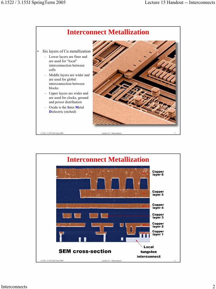
Interconnect Metal RC Delay
W
tmtox
L
Metal Ground PlaneSilicon Dioxide
Metal Line
RI =ρ
tm
LW
; CI =εitox
LW
RICI = ρtm
LW
εitox
LW
= ρtm
εitox
L2
• need low ρ to minimize RC delay• need low εi to minimize RC delay• need to increase tm and tox to minimize RC delay
ρ is the resistivity of metalεi is the dielectric constant
6.152J / 3.155J Fall Term 2005 Lecture 15 -- Interconnects 8
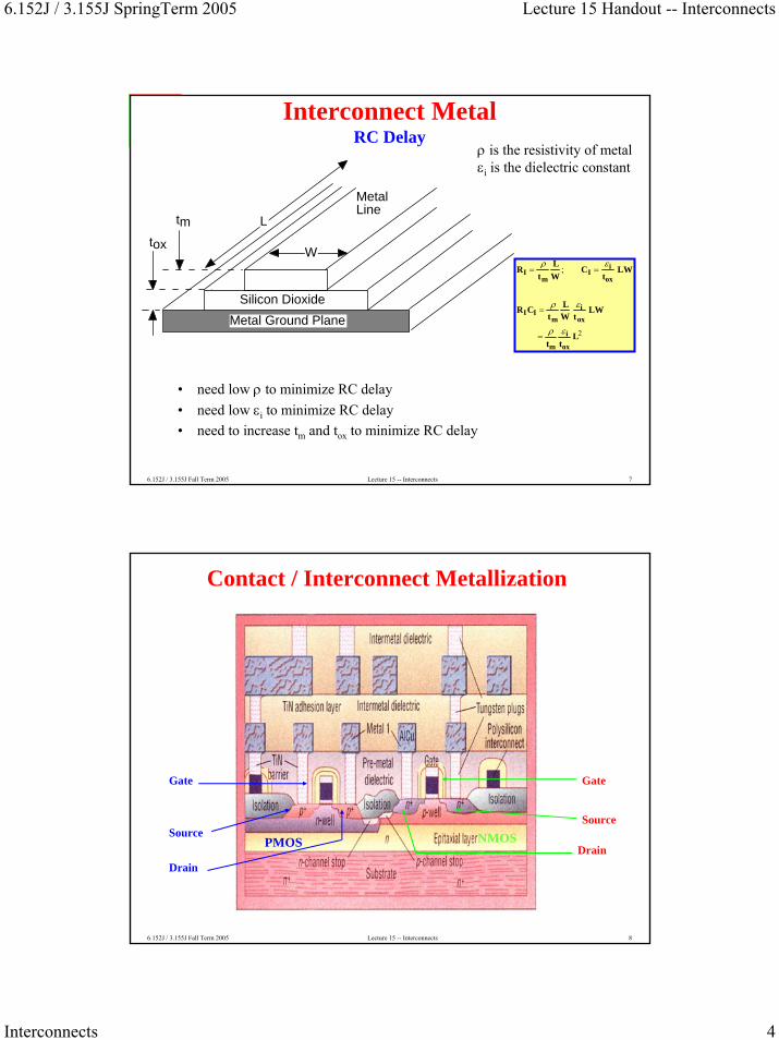
Contact / Interconnect Metallization
Gate
Source
Drain
PMOS
Gate
Source
DrainNMOS

6.152J / 3.155J SpringTerm 2005 Lecture 15 Handout -- Interconnects
Interconnects 5
6.152J / 3.155J Fall Term 2005 Lecture 15 -- Interconnects 9
Passive Devices
• Thin Film Resistors– CrSix, Pt, TaNx, ZrOx Poly-Si
• Capacitors– MOS capacitors– Parallel plate capacitors
• Inductors– Spiral inductors
Examples of Inductors
6.152J / 3.155J Fall Term 2005 Lecture 15 -- Interconnects 10
What are the desirable interconnect “wiring” properties?• Electrical
– Low resistance– Low ohmic contact resistance to Si
• Physical– Adhesion to all surfaces– Good step coverage– Stable and reliable (corrosion and electromigration resistant)
• Process Compatibility– Can easily be anisotropically etched– Survive subsequent processing steps
• Al used to be the pre-dominant metal for VLSI because it meets all the requirements stated above or has a way around any problems
• Cu is now the metal for IC interconnects
Which Metal(s)?
6.152J / 3.155J SpringTerm 2005 Lecture 15 Handout -- Interconnects
Interconnects 6
6.152J / 3.155J Fall Term 2005 Lecture 15 -- Interconnects 11
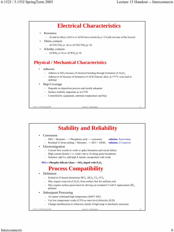
Electrical Characteristics• Resistance
– Al and its alloys (Al/Cu or Al/Si) have resistivity ρ=3.0 µΩ-cm (one of the lowest)• Ohmic contacts
– Al/TiN/TiSi2/n+-Si or Al/TiN/TiSi2/p+-Si• Schottky contacts
– Al/WSix/n--Si or Al/WSix/p--Si
Physical / Mechanical Characteristics• Adhesion
– Adheres to SiO2 because of chemical bonding through formation of Al2O3
– Adheres to Si because of formation of Al/Si Eutectic alloy @ 577°C (can lead to spiking)
• Step Coverage– Depends on deposition process and mostly adequate– Surface mobility important as in CVD– Controlled by equipment, substrate temperature and bias
6.152J / 3.155J Fall Term 2005 Lecture 15 -- Interconnects 12
Stability and Reliability• Corrossion
– PSG + Moisture —> Phosphoric acid—> corrosion; solution: Passivation– Residual Cl from etching + Moisture —> HCl + AlOH; solution: Cl removal
• Electromigration– Current flow results in voids or spike formation and circuit failure– High current desnity-> e- wind->move Al along grain boundaries– Solution: add Cu, add high Z metals, encapsulate with oxide
Process Compatibility• Definition
– Etched in Cl-based chemistries BCl3, SiCl4, Cl2, CCl4– May require removal of Al2O3 from surface first for uniform etch– May require surface passivation by driving out residual Cl with F replacement (SF6
plasma)
• Subsequent Processing– Al cannot withstand high temperature (660°C MT)– Use low temperature oxide (LTO) as inter-level dielectric (ILD)– Change metallization to refractory metals if high temp is absolutely necessary
PSG ≡ Phospho-Silicate Glass —SiO2 doped with P2O5
6.152J / 3.155J SpringTerm 2005 Lecture 15 Handout -- Interconnects
Interconnects 7
6.152J / 3.155J Fall Term 2005 Lecture 15 -- Interconnects 13
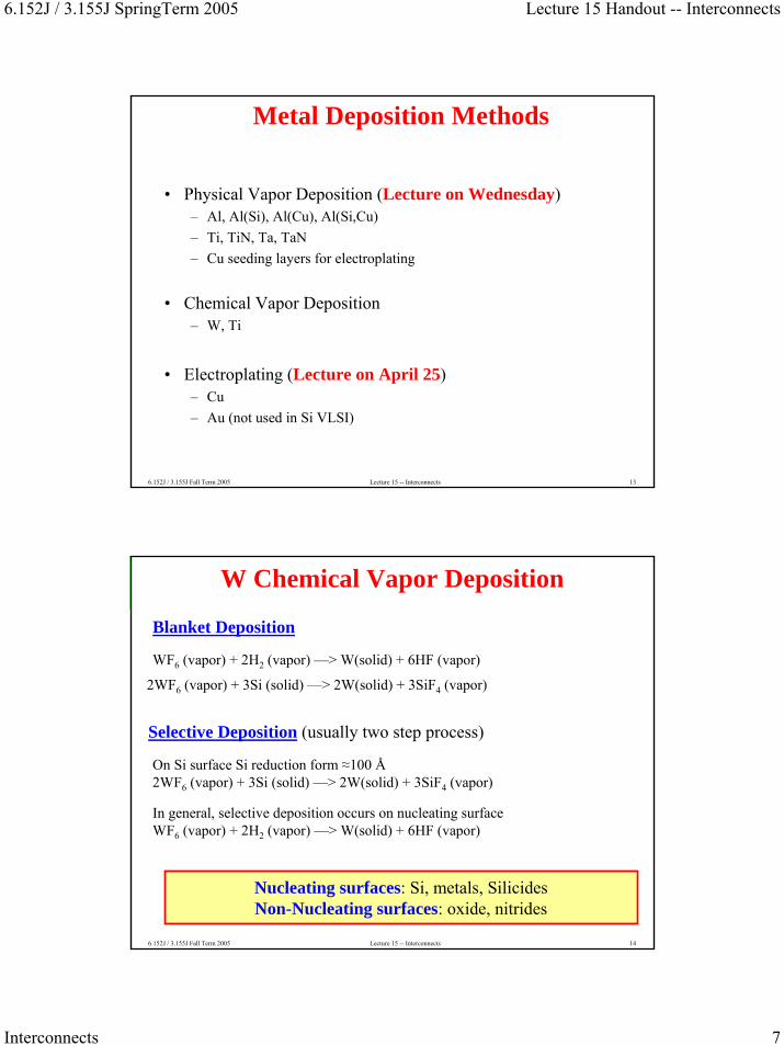
Metal Deposition Methods
• Physical Vapor Deposition (Lecture on Wednesday)– Al, Al(Si), Al(Cu), Al(Si,Cu)– Ti, TiN, Ta, TaN– Cu seeding layers for electroplating
• Chemical Vapor Deposition– W, Ti
• Electroplating (Lecture on April 25)– Cu– Au (not used in Si VLSI)
6.152J / 3.155J Fall Term 2005 Lecture 15 -- Interconnects 14
W Chemical Vapor Deposition
Blanket Deposition
WF6 (vapor) + 2H2 (vapor) —> W(solid) + 6HF (vapor)
2WF6 (vapor) + 3Si (solid) —> 2W(solid) + 3SiF4 (vapor)
Selective Deposition (usually two step process)
On Si surface Si reduction form ≈100 Å2WF6 (vapor) + 3Si (solid) —> 2W(solid) + 3SiF4 (vapor)
In general, selective deposition occurs on nucleating surfaceWF6 (vapor) + 2H2 (vapor) —> W(solid) + 6HF (vapor)
Nucleating surfaces: Si, metals, SilicidesNon-Nucleating surfaces: oxide, nitrides

6.152J / 3.155J SpringTerm 2005 Lecture 15 Handout -- Interconnects
Interconnects 8
6.152J / 3.155J Fall Term 2005 Lecture 15 -- Interconnects 15
Cu Electroplating• Copper is deposited by
– Sputtering (seeding layer for electroplating)
– Electroplating• Plating solutions contain
Copper sulfate / Sulfuric acid – Many additives to control
texture• Copper is a fast diffuser in Si
and it also a contaminant– Require a liner or diffusion
barrier such as TaN
500 Å TaNLiner/barrier layer1000 Å sputtered CuSeeding layer
6.152J / 3.155J Fall Term 2005 Lecture 15 -- Interconnects 16
Interconnect Definition• Subtractive Etch
– Deposit metal by sputtering– Pattern with photoresist– Etch metal from areas not needed– Strip photoresist
• Lift-Off– Pattern Photoresist– Deposit metal by e-beam evaporation (everywhere)– Dissolve photoresist to lift-off metal from field region
• Damascene– Deposit dielectric– Pattern photo-resist– Etch dielectric using PR as mask– Strip PR– Deposit Metal – Polish metal to be level with dielectric in field regions

6.152J / 3.155J SpringTerm 2005 Lecture 15 Handout -- Interconnects
Interconnects 9
6.152J / 3.155J Fall Term 2005 Lecture 15 -- Interconnects 17
Lift-Off(III-V Electronic /Optoelectronic Devices)
• Chlorobenzene Assisted Lift-off– Pattern Photoresist– Soak in chlorobenzene to make the photoresist swell and form a “lip”– Deposit metal by e-beam evaporation– Dissolve photoresist to lift-off metal from field region
• Dielectric assisted lift-off (DALO) avoids chlorobenzene soak– Deposit dieletric which has same thickness as metal to be deposited– Pattern resist and etch dielectric by RIE– Use BOE (or isotropic over-etch) to form “lip”
6.152J / 3.155J Fall Term 2005 Lecture 15 -- Interconnects 18
Damasene
• Pattern photoresist• Etch hole/trench in
dielectric• Fill holes / trenches with
metal• Etch back the metal
– Plasma etch back– Chemical Mechanical
Polishing
Etch back W
6.152J / 3.155J SpringTerm 2005 Lecture 15 Handout -- Interconnects
Interconnects 10
6.152J / 3.155J Fall Term 2005 Lecture 15 -- Interconnects 19
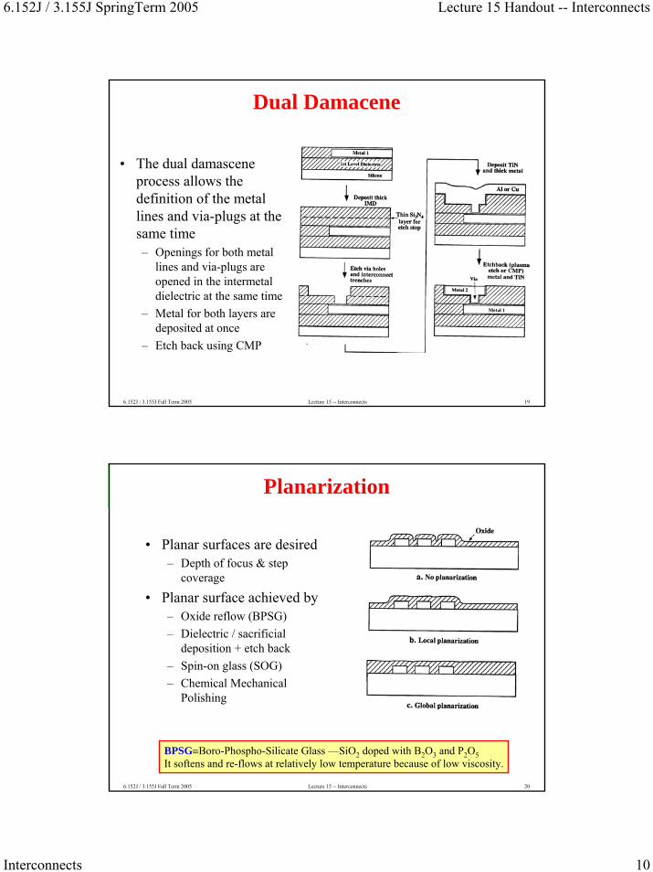
Dual Damacene
• The dual damascene process allows the definition of the metal lines and via-plugs at the same time– Openings for both metal
lines and via-plugs are opened in the intermetaldielectric at the same time
– Metal for both layers are deposited at once
– Etch back using CMP
6.152J / 3.155J Fall Term 2005 Lecture 15 -- Interconnects 20
Planarization
• Planar surfaces are desired– Depth of focus & step
coverage
• Planar surface achieved by– Oxide reflow (BPSG)– Dielectric / sacrificial
deposition + etch back– Spin-on glass (SOG)– Chemical Mechanical
Polishing
BPSG≡Boro-Phospho-Silicate Glass —SiO2 doped with B2O3 and P2O5It softens and re-flows at relatively low temperature because of low viscosity.
6.152J / 3.155J SpringTerm 2005 Lecture 15 Handout -- Interconnects
Interconnects 11
6.152J / 3.155J Fall Term 2005 Lecture 15 -- Interconnects 21
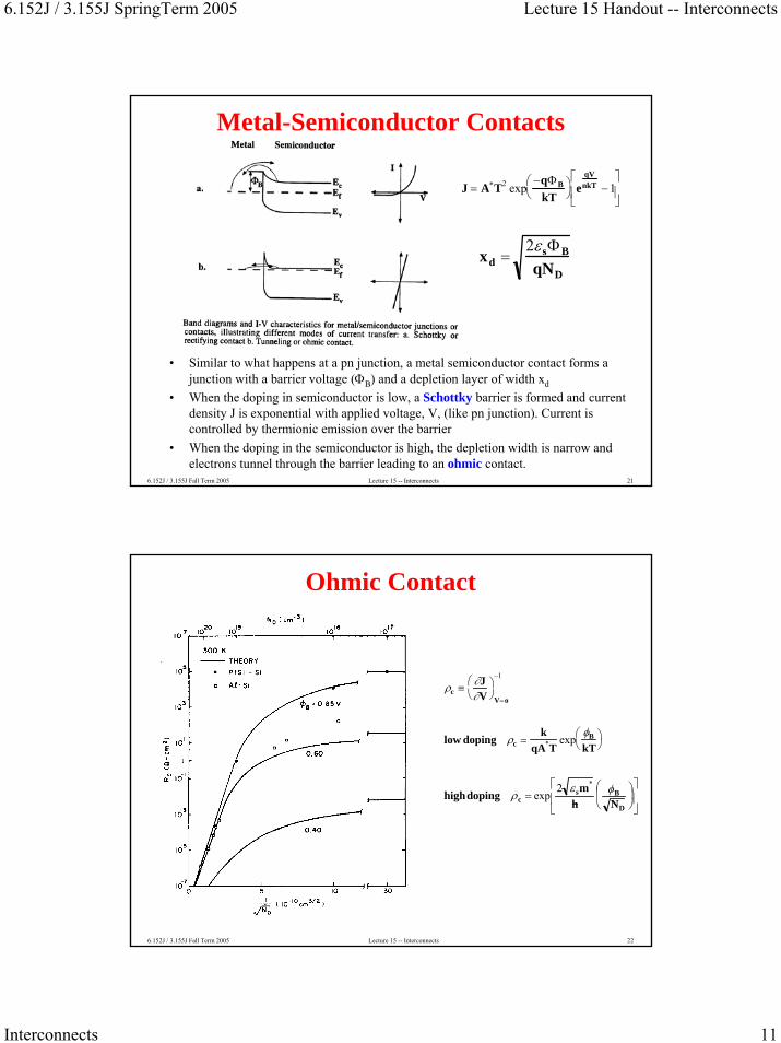
Metal-Semiconductor Contacts
• Similar to what happens at a pn junction, a metal semiconductor contact forms a junction with a barrier voltage (ΦB) and a depletion layer of width xd
• When the doping in semiconductor is low, a Schottky barrier is formed and current density J is exponential with applied voltage, V, (like pn junction). Current is controlled by thermionic emission over the barrier
• When the doping in the semiconductor is high, the depletion width is narrow and electrons tunnel through the barrier leading to an ohmic contact.
J = A∗T2 exp−qΦB
kT⎛ ⎝
⎞ ⎠ e
qVnkT −1
⎡
⎣ ⎢
⎤
⎦ ⎥
xd =2εsΦB
qND
6.152J / 3.155J Fall Term 2005 Lecture 15 -- Interconnects 22
Ohmic Contact
ρc ≡ ∂J∂V
⎛ ⎝
⎞ ⎠ V=o
−1
low doping ρc =k
qA*Texp
φB
kT⎛ ⎝
⎞ ⎠
highdoping ρc = exp2 εsm
*
h φBND
⎛
⎝ ⎜ ⎞
⎠ ⎟
⎡
⎣ ⎢
⎤
⎦ ⎥
6.152J / 3.155J SpringTerm 2005 Lecture 15 Handout -- Interconnects
Interconnects 12
6.152J / 3.155J Fall Term 2005 Lecture 15 -- Interconnects 23
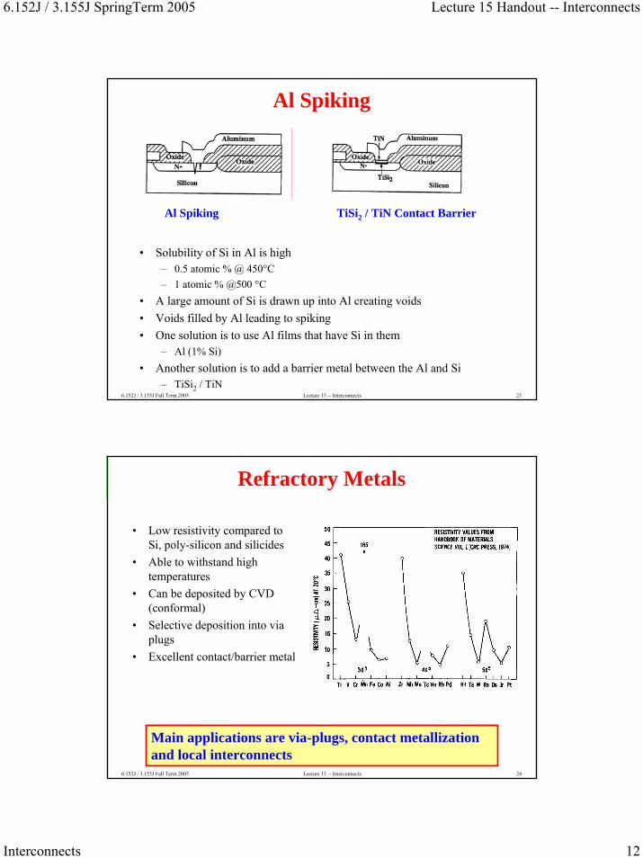
Al Spiking
• Solubility of Si in Al is high– 0.5 atomic % @ 450°C– 1 atomic % @500 °C
• A large amount of Si is drawn up into Al creating voids• Voids filled by Al leading to spiking• One solution is to use Al films that have Si in them
– Al (1% Si)• Another solution is to add a barrier metal between the Al and Si
– TiSi2 / TiN
Al Spiking TiSi2 / TiN Contact Barrier
6.152J / 3.155J Fall Term 2005 Lecture 15 -- Interconnects 24
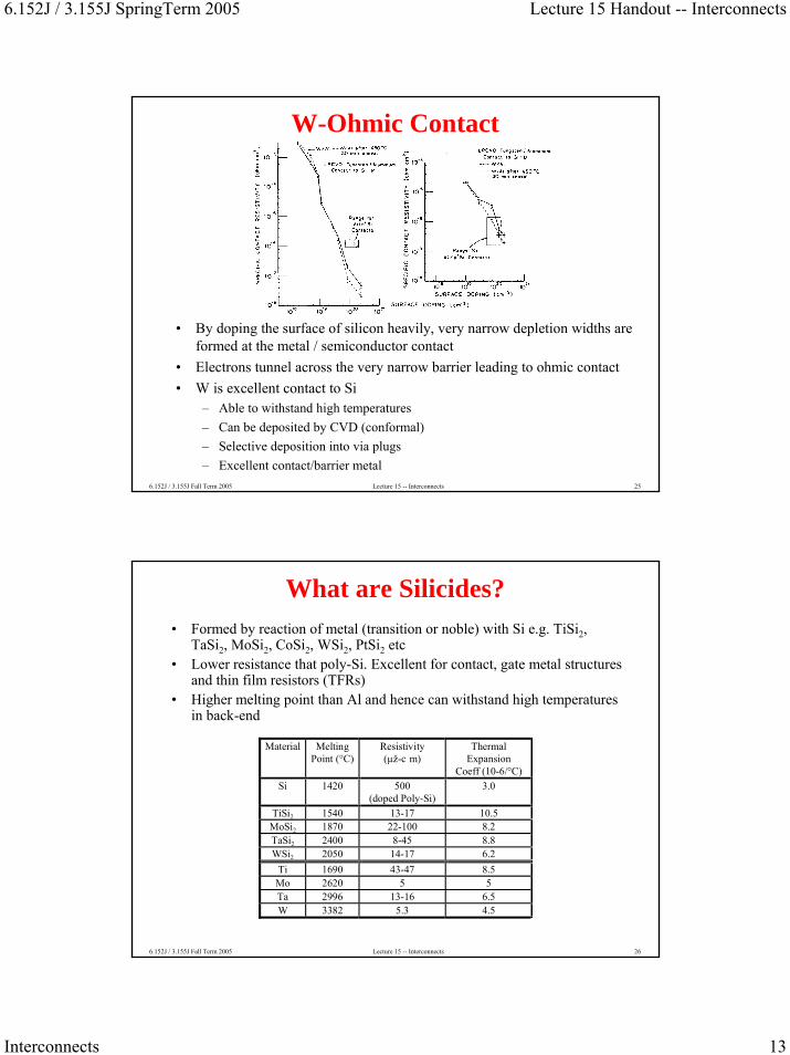
Refractory Metals
• Low resistivity compared to Si, poly-silicon and silicides
• Able to withstand high temperatures
• Can be deposited by CVD (conformal)
• Selective deposition into via plugs
• Excellent contact/barrier metal
Main applications are via-plugs, contact metallization and local interconnects
6.152J / 3.155J SpringTerm 2005 Lecture 15 Handout -- Interconnects
Interconnects 13
6.152J / 3.155J Fall Term 2005 Lecture 15 -- Interconnects 25
W-Ohmic Contact
• By doping the surface of silicon heavily, very narrow depletion widths are formed at the metal / semiconductor contact
• Electrons tunnel across the very narrow barrier leading to ohmic contact• W is excellent contact to Si
– Able to withstand high temperatures– Can be deposited by CVD (conformal)– Selective deposition into via plugs– Excellent contact/barrier metal
6.152J / 3.155J Fall Term 2005 Lecture 15 -- Interconnects 26
What are Silicides?• Formed by reaction of metal (transition or noble) with Si e.g. TiSi2,
TaSi2, MoSi2, CoSi2, WSi2, PtSi2 etc• Lower resistance that poly-Si. Excellent for contact, gate metal structures
and thin film resistors (TFRs)• Higher melting point than Al and hence can withstand high temperatures
in back-end
Material MeltingPoint (°C)
Resistivity(µž-c m)
ThermalExpansion
Coeff (10-6/°C)Si 1420 500
(doped Poly-Si)3.0
TiSi2 1540 13-17 10.5MoSi2 1870 22-100 8.2TaSi2 2400 8-45 8.8WSi2 2050 14-17 6.2
Ti 1690 43-47 8.5Mo 2620 5 5Ta 2996 13-16 6.5W 3382 5.3 4.5
6.152J / 3.155J SpringTerm 2005 Lecture 15 Handout -- Interconnects
Interconnects 14
6.152J / 3.155J Fall Term 2005 Lecture 15 -- Interconnects 27
Silicide Materials Requirements
• Low resistivity• Ease of formation• Ease of fine line
patterning• Controlled oxidation
properties• High temperature stability• Smooth surface features• Corrosion resistance
• Stable contact formation to Si and Al
• Excellent Adhesion• Low stress• Electromigration resistance• Low ohmic and contact
resistance• Stability during high
temperature processing
6.152J / 3.155J Fall Term 2005 Lecture 15 -- Interconnects 28
Methods of Silicide Formation
• Direct Metallurgical Reaction with metal deposited by evaporation, sputter or CVD– M + xSi—>MSix
• Co-evaporation from independent Si and M source• Co sputtering from Independent Si and M targets• Sputtering from a composite MSix target• Chemical vapor deposition

6.152J / 3.155J SpringTerm 2005 Lecture 15 Handout -- Interconnects
Interconnects 15
6.152J / 3.155J Fall Term 2005 Lecture 15 -- Interconnects 29
Applications of Silicides
• Gate metallization (Polycide)—1
• Ohmic contact / barrier metal (Salicide Technology) —2
• Local Interconnects—3• Thin-Film Resistors
6.152J / 3.155J Fall Term 2005 Lecture 15 -- Interconnects 30
PolycidePoly-Silicon / Silicide
• Formed by depositing metal on poly-silicon and reacting to form silicide+ poly-silicon
– Deposit Metal– Heat to form silicide– Etch excess metal selectively
• Used principally to reduce gate resistance of MOS devices• Has the workfunction of poly-Silicon• Has a reliable poly-Si/SiO2 interface• Can be passivated by oxidation
Poly-silicon
Silicide
Poly-silicon Poly-silicon
MetalMetal
Silicide
Metal Desposition
Silicide Formation
Excess Metal Etched Away
Polycide
6.152J / 3.155J SpringTerm 2005 Lecture 15 Handout -- Interconnects
Interconnects 16
6.152J / 3.155J Fall Term 2005 Lecture 15 -- Interconnects 31
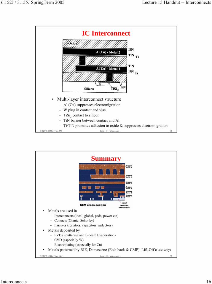
IC Interconnect
• Multi-layer interconnect structure– Al (Cu) suppresses electromigration– W plug in contact and vias– TiSi2 contact to silicon– TiN barrier between contact and Al– Ti/TiN promotes adhesion to oxide & suppresses electromigration
6.152J / 3.155J Fall Term 2005 Lecture 15 -- Interconnects 32
Summary
• Metals are used in– Interconnects (local, global, pads, power etc)– Contacts (Ohmic, Schottky)– Passives (resistors, capacitors, inductors)
• Metals deposited by– PVD (Sputtering and E-beam Evaporation)– CVD (especially W)– Electroplating (especially for Cu)
• Metals patterned by RIE, Damascene (Etch back & CMP), Lift-Off (GaAs only)
Recommended