1
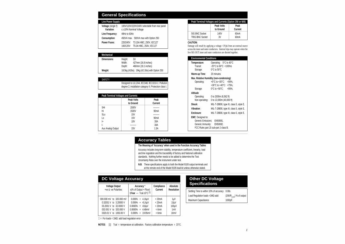
General Specifications
Line Power Supply
Voltage (single f): 100V/120V/220V/240V selectable from rear panelVariation: ≤ ±10% Nominal Voltage
Line Frequency: 48Hz to 63Hz
Consumption: 450VA max. 500VA max with Option 250
Power Fuses: 220/240V: T3.15A HBC, 250V, IEC127100/120V: T5.0A HBC, 250V, IEC127
NOTES: [1] Tcal = temperature at calibration. Factory calibration temperature = 23°C.
DC Voltage Accuracy
Voltage Output Accuracy * Compliance Absolute+ve & -ve Polarities ±(% of Output + Floor) Current Resolution
1Year — Tcal ±5°C [1]
000.000 mV to 320.000 mV 0.006% + 4.16µV < 20mA 1µV0.32001 V to 3.20000 V 0.006% + 41.6µV < 20mA 10µV03.2001 V to 32.0000 V 0.0065% + 416µV < 20mA 100µV032.001 V to 320.000 V 0.0065% + 4.48mV < 6mA 1mV0320.01 V to 1050.00 V 0.006% + 19.95mV < 6mA 10mV
∗ = For loads < 1MΩ: add load regulation error.
The Meaning of 'Accuracy' when used in the Function Accuracy Tables
Accuracy includes long-term stability, temperature coefficient, linearity, loadand line regulation and the traceability of factory and National calibrationstandards. Nothing further needs to be added to determine the TestUncertainty Ratio over the instrument under test.
N.B. These specifications apply to both the Model 9100 output terminals andat the remote end of the Model 9105 lead kit unless otherwise stated.
Accuracy Tables
Mechanical
Dimensions: Height: 3UWidth: 427mm (16.8 inches)Depth: 460mm (18.1 inches)
Weight: 18.5kg (41lbs). 19kg (42.1lbs) with Option 250
SAFETYDesigned to UL1244, IEC348, IEC1010-1: Pollutiondegree 2; installation category II; Protection class I.
Peak Terminal Voltages and CurrentsPeak Volts Peakto Ground Current
SHi 1500V ———Hi 1500V 90mASLo 15V ———Lo 15V 90mAI+ 10V 30AI- ——— 30AAux Analog Output 15V 1.5A
Environmental Conditions
Temperature: Operating: 5°C to 40°CTransit: -20°C to 60°C <100hrsStorage: 0°C to 50°C
Warm-up Time: 20 minutes
Max. Relative Humidity (non-condensing):Operating: +5°C to +30°C: <90%,
+30°C to +40°C: <75%,Storage: 0°C to +50°C: <95%,
AltitudeOperating: 0 to 2000m (6,562 ft)Non-operating: 0 to 12,000m (40,000 ft)
Shock: MIL-T-28800, type III, class 5, style E.
Vibration: MIL-T-28800, type III, class 5, style E.
Enclosure: MIL-T-28800, type III, class 5, style E.
EMC: Designed to:Generic Emissions: EN50081.Generic Immunity: EN50082.FCC Rules part 15 sub-part J class B.
Other DC VoltageSpecifications
Settling Time to within 10% of accuracy: 0.08s
Load Regulation loads <1MΩ add: (200/RLOAD) % of output
Maximum Capacitance: 1000pF.
CAUTION:Damage will result by applying a voltage >3Vpk from an external sourceacross the inner and outer conductors. Internal trips may operate when thelive SIG OUT inner and outer conductors are shorted together.
Peak Terminal Voltages and Currents (Option 250 or 600)Peak Volts Peakto Ground Current
SIG BNC Socket 140V 60mATRIG BNC Socket 3V 60mA
2
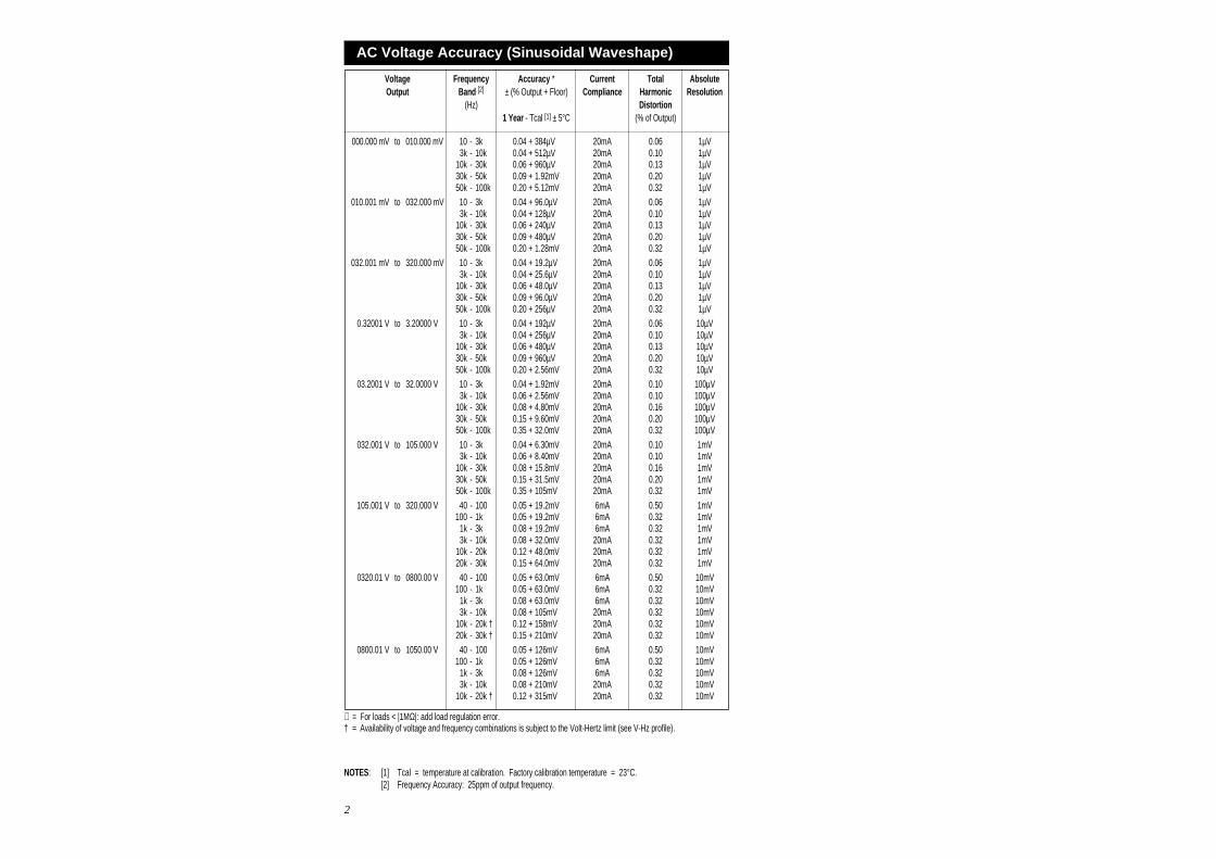
NOTES: [1] Tcal = temperature at calibration. Factory calibration temperature = 23°C.[2] Frequency Accuracy: 25ppm of output frequency.
∗ = For loads < |1MΩ|: add load regulation error.† = Availability of voltage and frequency combinations is subject to the Volt-Hertz limit (see V-Hz profile).
Voltage Frequency Accuracy * Current Total AbsoluteOutput Band [2] ± (% Output + Floor) Compliance Harmonic Resolution
(Hz) Distortion1 Year - Tcal [1] ± 5°C (% of Output)
000.000 mV to 010.000 mV 10 - 3k 0.04 + 384µV 20mA 0.06 1µV3k - 10k 0.04 + 512µV 20mA 0.10 1µV
10k - 30k 0.06 + 960µV 20mA 0.13 1µV30k - 50k 0.09 + 1.92mV 20mA 0.20 1µV50k - 100k 0.20 + 5.12mV 20mA 0.32 1µV
010.001 mV to 032.000 mV 10 - 3k 0.04 + 96.0µV 20mA 0.06 1µV3k - 10k 0.04 + 128µV 20mA 0.10 1µV
10k - 30k 0.06 + 240µV 20mA 0.13 1µV30k - 50k 0.09 + 480µV 20mA 0.20 1µV50k - 100k 0.20 + 1.28mV 20mA 0.32 1µV
032.001 mV to 320.000 mV 10 - 3k 0.04 + 19.2µV 20mA 0.06 1µV3k - 10k 0.04 + 25.6µV 20mA 0.10 1µV
10k - 30k 0.06 + 48.0µV 20mA 0.13 1µV30k - 50k 0.09 + 96.0µV 20mA 0.20 1µV50k - 100k 0.20 + 256µV 20mA 0.32 1µV
0.32001 V to 3.20000 V 10 - 3k 0.04 + 192µV 20mA 0.06 10µV3k - 10k 0.04 + 256µV 20mA 0.10 10µV
10k - 30k 0.06 + 480µV 20mA 0.13 10µV30k - 50k 0.09 + 960µV 20mA 0.20 10µV50k - 100k 0.20 + 2.56mV 20mA 0.32 10µV
03.2001 V to 32.0000 V 10 - 3k 0.04 + 1.92mV 20mA 0.10 100µV3k - 10k 0.06 + 2.56mV 20mA 0.10 100µV
10k - 30k 0.08 + 4.80mV 20mA 0.16 100µV30k - 50k 0.15 + 9.60mV 20mA 0.20 100µV50k - 100k 0.35 + 32.0mV 20mA 0.32 100µV
032.001 V to 105.000 V 10 - 3k 0.04 + 6.30mV 20mA 0.10 1mV3k - 10k 0.06 + 8.40mV 20mA 0.10 1mV
10k - 30k 0.08 + 15.8mV 20mA 0.16 1mV30k - 50k 0.15 + 31.5mV 20mA 0.20 1mV50k - 100k 0.35 + 105mV 20mA 0.32 1mV
105.001 V to 320.000 V 40 - 100 0.05 + 19.2mV 6mA 0.50 1mV100 - 1k 0.05 + 19.2mV 6mA 0.32 1mV
1k - 3k 0.08 + 19.2mV 6mA 0.32 1mV3k - 10k 0.08 + 32.0mV 20mA 0.32 1mV
10k - 20k 0.12 + 48.0mV 20mA 0.32 1mV20k - 30k 0.15 + 64.0mV 20mA 0.32 1mV
0320.01 V to 0800.00 V 40 - 100 0.05 + 63.0mV 6mA 0.50 10mV100 - 1k 0.05 + 63.0mV 6mA 0.32 10mV
1k - 3k 0.08 + 63.0mV 6mA 0.32 10mV3k - 10k 0.08 + 105mV 20mA 0.32 10mV
10k - 20k † 0.12 + 158mV 20mA 0.32 10mV20k - 30k † 0.15 + 210mV 20mA 0.32 10mV
0800.01 V to 1050.00 V 40 - 100 0.05 + 126mV 6mA 0.50 10mV100 - 1k 0.05 + 126mV 6mA 0.32 10mV
1k - 3k 0.08 + 126mV 6mA 0.32 10mV3k - 10k 0.08 + 210mV 20mA 0.32 10mV
10k - 20k † 0.12 + 315mV 20mA 0.32 10mV
AC Voltage Accuracy (Sinusoidal Waveshape)
3
TTL Signals 1V to 3V RMS Sine Input †Voltage Selected Output Phase Error Output Phase Error Output Phase ErrorOutput Frequency with respect to with respect to with respect to
f (Hz) 'Phase Lock In' 'Phase Lock Out' 'Phase Lock In'
0.30000 V to 105.000 V 10 - 40 ±0.07° ±0.07° ±0.70°40 - 65 ±0.07° ±0.07° ±0.14°65 - 1k ±(0.07 + 0.001 x f)° ±(0.07 + 0.001 x f)° ±(0.14 + 0.001 x f)°
105.001 V to 0750.00 V ♦ 45 - 65 ±0.16° ±0.16° ±0.23°65 - 1k ±(0.16 + 0.0037 x f)° ±(0.16 + 0.0037 x f)° ±(0.23 + 0.0037 x f)°
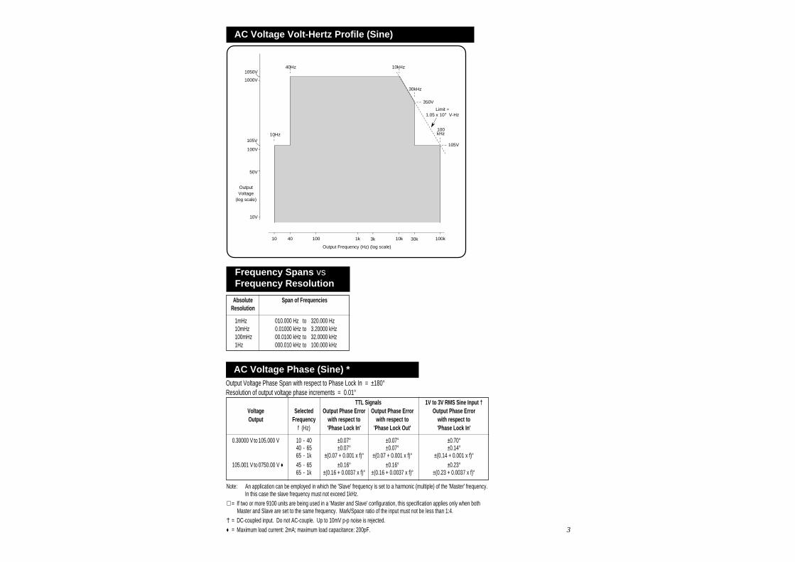
AC Voltage Volt-Hertz Profile (Sine)
100V
40Hz
Output Frequency (Hz) (log scale)
Output Voltage
(log scale)
40 3k
50V
10 1k
1000V
10V
10Hz
10kHz
30kHz
100
Limit =1.05 x 10⁷ V-Hz
350V
105V105V
1050V
100kHz
30k 100k10k
Absolute Span of FrequenciesResolution
1mHz 010.000 Hz to 320.000 Hz10mHz 0.01000 kHz to 3.20000 kHz100mHz 00.0100 kHz to 32.0000 kHz1Hz 000.010 kHz to 100.000 kHz
Frequency Spans vsFrequency Resolution
AC Voltage Phase (Sine) *Output Voltage Phase Span with respect to Phase Lock In = ±180°Resolution of output voltage phase increments = 0.01°
Note: An application can be employed in which the 'Slave' frequency is set to a harmonic (multiple) of the 'Master' frequency.In this case the slave frequency must not exceed 1kHz.
∗ = If two or more 9100 units are being used in a 'Master and Slave' configuration, this specification applies only when bothMaster and Slave are set to the same frequency. Mark/Space ratio of the input must not be less than 1:4.
† = DC-coupled input. Do not AC-couple. Up to 10mV p-p noise is rejected.♦ = Maximum load current: 2mA; maximum load capacitance: 200pF.
4
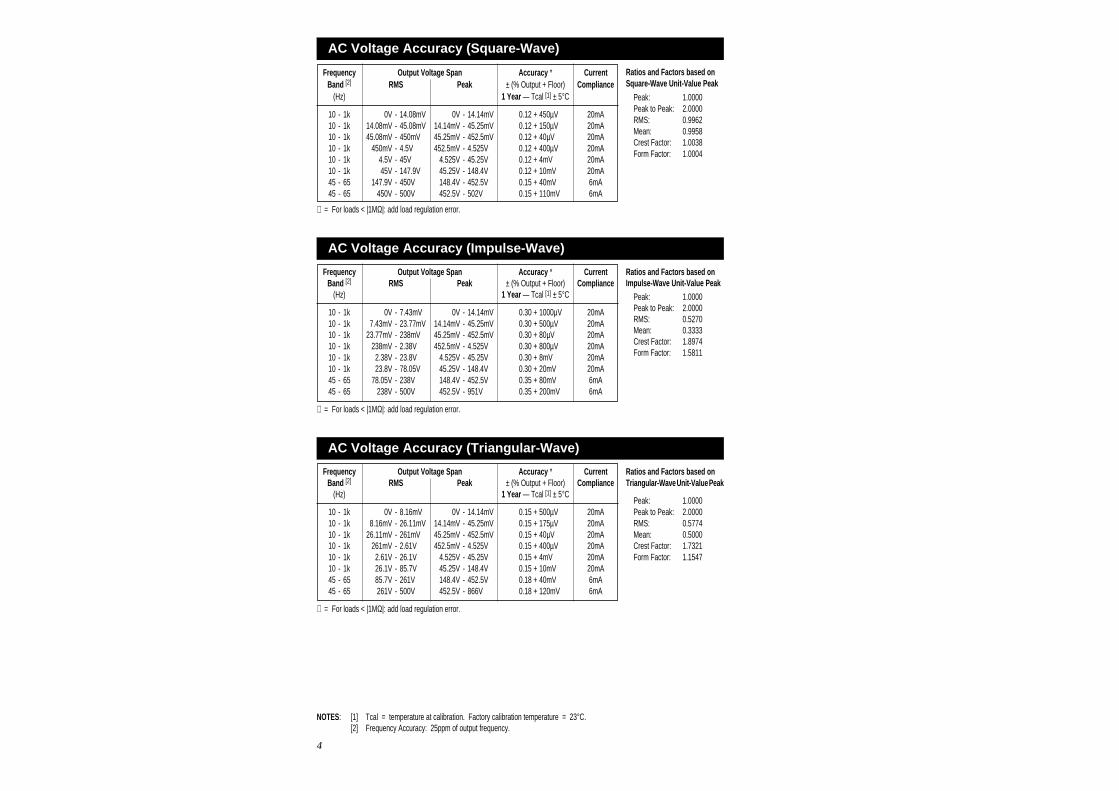
AC Voltage Accuracy (Square-Wave)
Ratios and Factors based onSquare-Wave Unit-Value Peak
Peak: 1.0000Peak to Peak: 2.0000RMS: 0.9962Mean: 0.9958Crest Factor: 1.0038Form Factor: 1.0004
∗ = For loads < |1MΩ|: add load regulation error.
Frequency Output Voltage Span Accuracy * CurrentBand [2] RMS Peak ± (% Output + Floor) Compliance
(Hz) 1 Year — Tcal [1] ± 5°C
10 - 1k 0V - 14.08mV 0V - 14.14mV 0.12 + 450µV 20mA10 - 1k 14.08mV - 45.08mV 14.14mV - 45.25mV 0.12 + 150µV 20mA10 - 1k 45.08mV - 450mV 45.25mV - 452.5mV 0.12 + 40µV 20mA10 - 1k 450mV - 4.5V 452.5mV - 4.525V 0.12 + 400µV 20mA10 - 1k 4.5V - 45V 4.525V - 45.25V 0.12 + 4mV 20mA10 - 1k 45V - 147.9V 45.25V - 148.4V 0.12 + 10mV 20mA45 - 65 147.9V - 450V 148.4V - 452.5V 0.15 + 40mV 6mA45 - 65 450V - 500V 452.5V - 502V 0.15 + 110mV 6mA
NOTES: [1] Tcal = temperature at calibration. Factory calibration temperature = 23°C.[2] Frequency Accuracy: 25ppm of output frequency.
AC Voltage Accuracy (Impulse-Wave)
∗ = For loads < |1MΩ|: add load regulation error.
Frequency Output Voltage Span Accuracy * CurrentBand [2] RMS Peak ± (% Output + Floor) Compliance
(Hz) 1 Year — Tcal [1] ± 5°C
10 - 1k 0V - 7.43mV 0V - 14.14mV 0.30 + 1000µV 20mA10 - 1k 7.43mV - 23.77mV 14.14mV - 45.25mV 0.30 + 500µV 20mA10 - 1k 23.77mV - 238mV 45.25mV - 452.5mV 0.30 + 80µV 20mA10 - 1k 238mV - 2.38V 452.5mV - 4.525V 0.30 + 800µV 20mA10 - 1k 2.38V - 23.8V 4.525V - 45.25V 0.30 + 8mV 20mA10 - 1k 23.8V - 78.05V 45.25V - 148.4V 0.30 + 20mV 20mA45 - 65 78.05V - 238V 148.4V - 452.5V 0.35 + 80mV 6mA45 - 65 238V - 500V 452.5V - 951V 0.35 + 200mV 6mA
Ratios and Factors based onImpulse-Wave Unit-Value Peak
Peak: 1.0000Peak to Peak: 2.0000RMS: 0.5270Mean: 0.3333Crest Factor: 1.8974Form Factor: 1.5811
AC Voltage Accuracy (Triangular-Wave)
∗ = For loads < |1MΩ|: add load regulation error.
Ratios and Factors based onTriangular-Wave Unit-Value Peak
Peak: 1.0000Peak to Peak: 2.0000RMS: 0.5774Mean: 0.5000Crest Factor: 1.7321Form Factor: 1.1547
Frequency Output Voltage Span Accuracy * CurrentBand [2] RMS Peak ± (% Output + Floor) Compliance
(Hz) 1 Year — Tcal [1] ± 5°C
10 - 1k 0V - 8.16mV 0V - 14.14mV 0.15 + 500µV 20mA10 - 1k 8.16mV - 26.11mV 14.14mV - 45.25mV 0.15 + 175µV 20mA10 - 1k 26.11mV - 261mV 45.25mV - 452.5mV 0.15 + 40µV 20mA10 - 1k 261mV - 2.61V 452.5mV - 4.525V 0.15 + 400µV 20mA10 - 1k 2.61V - 26.1V 4.525V - 45.25V 0.15 + 4mV 20mA10 - 1k 26.1V - 85.7V 45.25V - 148.4V 0.15 + 10mV 20mA45 - 65 85.7V - 261V 148.4V - 452.5V 0.18 + 40mV 6mA45 - 65 261V - 500V 452.5V - 866V 0.18 + 120mV 6mA
5
∗ = For loads < |1MΩ|: add load regulation error.
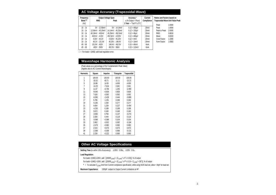
AC Voltage Accuracy (Trapezoidal-Wave)
Frequency Output Voltage Span Accuracy * CurrentBand [2] RMS Peak ± (% Output + Floor) Compliance
(Hz) 1 Year — Tcal [1] ± 5°C
10 - 1k 0V - 12.56mV 0V - 14.14mV 0.12 + 450µV 20mA10 - 1k 12.56mV - 40.19mV 14.14mV - 45.25mV 0.12 + 150µV 20mA10 - 1k 40.19mV - 402mV 45.25mV - 452.5mV 0.12 + 40µV 20mA10 - 1k 402mV - 4.02V 452.5mV - 4.525V 0.12 + 400µV 20mA10 - 1k 4.02V - 40.2V 4.525V - 45.25V 0.12 + 4mV 20mA10 - 1k 40.2V - 131.9V 45.25V - 148.4V 0.12 + 10mV 20mA45 - 65 131.9V - 402V 148.4V - 452.5V 0.15 + 40mV 6mA45 - 65 402V - 500V 452.5V - 566V 0.15 + 110mV 6mA
Ratios and Factors based onTrapezoidal-Wave Unit-Value Peak
Peak: 1.0000Peak: 1.0000Peak to Peak: 2.0000RMS: 0.8819Mean: 0.8333Crest Factor: 1.3390Form Factor: 1.0583
Waveshape Harmonic Analysis(Peak values as a percentage of the Fundamental's Peak Value)(Applies also to AC Current Waveshapes)
Harmonic Square Impulse Triangular Trapezoidal
1 100.00 100.00 100.00 100.003 -33.32 60.71 11.11 -22.225 19.98 14.93 4.000 4.0007 -14.25 -7.616 2.041 2.0419 11.07 -6.746 1.235 -2.46911 -9.040 -0.826 0.826 0.82613 7.626 -0.592 0.592 0.59215 -6.590 -2.428 0.444 -0.88917 5.795 -1.291 0.346 0.34619 -5.165 1.034 0.277 0.27721 4.654 1.239 0.227 -0.45423 -4.230 0.189 0.189 0.18925 3.872 0.160 0.160 0.16027 -3.565 0.750 0.137 -0.27429 3.300 0.444 0.119 0.11931 -3.068 -0.388 0.104 0.10433 2.862 -0.502 0.092 -0.18435 -2.679 -0.082 0.082 0.08237 2.515 -0.073 0.073 0.07339 -2.368 -0.359 0.066 -0.13141 2.230 -0.222 0.060 0.060
Other AC Voltage Specifications
Settling Time (to within 10% of accuracy): ≤105V: 0.08s; >105V: 0.5s.
Load Regulation:
For loads <|1MΩ| ≤105V, add: [(200/RLOAD) + (CLOAD* x F2 x 0.03)] % of output
For loads <|1MΩ| >105V, add: [(200/RLOAD) + (CLOAD* x F2 x 0.19 + CLOAD* • 3E7)] % of output
* = To calculate CLOAD limit from Current compliance specification, while using 9105 lead set, allow ≈ 30pF for lead set.
Maximum Capacitance: 1000pF; subject to Output Current Limitations at HF.
6
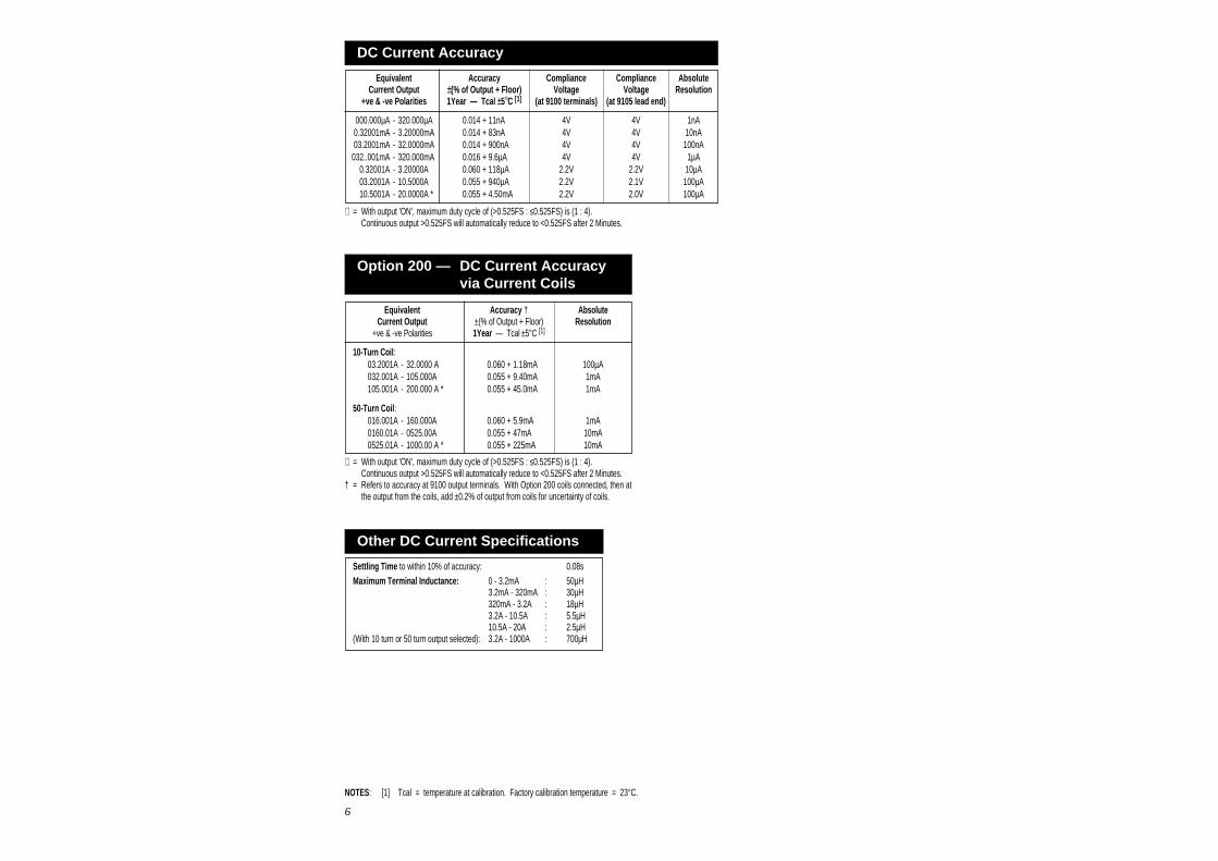
DC Current Accuracy
NOTES: [1] Tcal = temperature at calibration. Factory calibration temperature = 23°C.
Equivalent Accuracy Compliance Compliance AbsoluteCurrent Output ±(% of Output + Floor) Voltage Voltage Resolution
+ve & -ve Polarities 1Year — Tcal ±5°C [1] (at 9100 terminals) (at 9105 lead end)
000.000µA - 320.000µA 0.014 + 11nA 4V 4V 1nA0.32001mA - 3.20000mA 0.014 + 83nA 4V 4V 10nA03.2001mA - 32.0000mA 0.014 + 900nA 4V 4V 100nA
032..001mA - 320.000mA 0.016 + 9.6µA 4V 4V 1µA0.32001A - 3.20000A 0.060 + 118µA 2.2V 2.2V 10µA03.2001A - 10.5000A 0.055 + 940µA 2.2V 2.1V 100µA10.5001A - 20.0000A * 0.055 + 4.50mA 2.2V 2.0V 100µA
∗ = With output 'ON', maximum duty cycle of (>0.525FS : ≤0.525FS) is (1 : 4).Continuous output >0.525FS will automatically reduce to <0.525FS after 2 Minutes.
Option 200 — DC Current Accuracyvia Current Coils
Equivalent Accuracy † AbsoluteCurrent Output ±(% of Output + Floor) Resolution
+ve & -ve Polarities 1Year — Tcal ±5°C [1]
10-Turn Coil:03.2001A - 32.0000 A 0.060 + 1.18mA 100µA032.001A - 105.000A 0.055 + 9.40mA 1mA105.001A - 200.000 A * 0.055 + 45.0mA 1mA
50-Turn Coil:016.001A - 160.000A 0.060 + 5.9mA 1mA0160.01A - 0525.00A 0.055 + 47mA 10mA0525.01A - 1000.00 A * 0.055 + 225mA 10mA
∗ = With output 'ON', maximum duty cycle of (>0.525FS : ≤0.525FS) is (1 : 4).Continuous output >0.525FS will automatically reduce to <0.525FS after 2 Minutes.
† = Refers to accuracy at 9100 output terminals. With Option 200 coils connected, then atthe output from the coils, add ±0.2% of output from coils for uncertainty of coils.
Other DC Current Specifications
Settling Time to within 10% of accuracy: 0.08sMaximum Terminal Inductance: 0 - 3.2mA : 50µH
3.2mA - 320mA : 30µH320mA - 3.2A : 18µH3.2A - 10.5A : 5.5µH10.5A - 20A : 2.5µH
(With 10 turn or 50 turn output selected): 3.2A - 1000A : 700µH
7
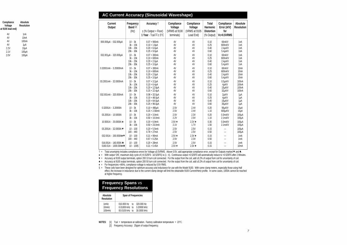
AC Current Accuracy (Sinusoidal Waveshape)
Current Frequency Accuracy † Compliance Compliance Total Compliance AbsoluteOutput Band [2] Voltage Voltage Harmonic Error (A/V) Resolution
(Hz) ± (% Output + Floor) (VRMS at 9100 (VRMS at 9105 Distortion for1 Year - Tcal [1] ± 5°C terminals) Lead End) (% Output) Vc>0.5VRMS
000.000µA - 032.000µA 10 - 3k 0.07 + 900nA 4V 4V 0.10 60nA/V 1nA3k - 10k 0.10 + 1.8µA 4V 4V 0.25 600nA/V 1nA
10k - 20k 0.20 + 6.0µA 4V 4V 0.40 2.4µA/V 1nA20k - 30k 0.25 + 9.0µA 4V 4V 0.60 5.4µA/V 1nA
032.001µA - 320.000µA 10 - 3k 0.07 + 300nA 4V 4V 0.10 60nA/V 1nA3k - 10k 0.10 + 600nA 4V 4V 0.25 600nA/V 1nA
10k - 20k 0.20 + 2.0µA 4V 4V 0.40 2.4µA/V 1nA20k - 30k 0.25 + 3.0µA 4V 4V 0.60 5.4µA/V 1nA
0.32001mA - 3.20000mA 10 - 3k 0.07 + 300nA 4V 4V 0.10 60nA/V 10nA3k - 10k 0.10 + 600nA 4V 4V 0.25 600nA/V 10nA
10k - 20k 0.20 + 2.0µA 4V 4V 0.40 2.4µA/V 10nA20k - 30k 0.25 + 3.0µA 4V 4V 0.60 5.4µA/V 10nA
03.2001mA - 32.0000mA 10 - 3k 0.07 + 3.2µA 4V 4V 0.10 0.5µA/V 100nA3k - 10k 0.10 + 6.4µA 4V 4V 0.25 4µA/V 100nA
10k - 20k 0.20 + 12.8µA 4V 4V 0.40 15µA/V 100nA20k - 30k 0.25 + 22.4µA 4V 4V 0.60 32µA/V 100nA
032.001mA - 320.000mA 10 - 3k 0.08 + 32.0µA 4V 4V 0.10 2µA/V 1µA3k - 10k 0.10 + 48.0µA 4V 4V 0.25 4µA/V 1µA
10k - 20k 0.20 + 64.0µA 4V 4V 0.40 15µA/V 1µA20k - 30k 0.25 + 96.0µA 4V 4V 0.60 35µA/V 1µA
0.32001A - 3.20000A 10 - 3k 0.10 + 480µA 2.5V 2.4V 0.20 90µA/V 10µA3k - 10k 0.25 + 2.56mA 2.5V 2.4V 1.10 600µA/V 10µA
03.2001A - 10.5000A 10 - 3k 0.20 + 3.0mA 2.5V 2.3V 0.20 0.3mA/V 100µA3k - 10k 0.50 + 10.0mA 2.2V 2.0V 1.10 2.1mA/V 100µA
10.5001A - 20.0000A ♠ 10 - 3k 0.20 + 6.9mA 2.5V ♦ 2.2V ♦ 0.30 0.3mA/V 100µA3k - 10k 0.50 + 23.0mA 2.1V 1.7V 1.50 2.1mA/V 100µA
03.2001A - 32.0000A ♥ 10 - 100 0.20 + 5.5mA 2.5V 2.5V 0.15 --- 100µA100 - 440 0.78 + 27mA 2.5V 2.5V 0.50 --- 100µA
032.001A - 200.000A♠♥ 10 - 100 0.21 + 90mA 2.5V ♦ 2.3V ♦ 0.15 --- 1mA100 - 440 0.67 + 0.25A 2.5V 2.3V 0.50 --- 1mA
016.001A - 160.000A ♣ 10 - 100 0.20 + 28mA 2.5V 2.5V 0.15 --- 1mA0160.01A - 1000.00A♠♣ 10 - 100§ 0.21 + 0.45A 2.5V ♦ 2.3V ♦ 0.15 --- 10mA
† = Total uncertainty includes compliance errors for Voltage ≤0.5VRMS. Above 0.5V, add appropriate compliance error, except for Outputs marked ♥ and ♣ .♠ = With output 'ON', maximum duty cycle of (>0.525FS : ≤0.525FS) is (1 : 4). Continuous output >0.525FS will automatically reduce to <0.525FS after 2 Minutes.♥ = Accuracy at 9100 output terminals, option 200 10 turn coil connected. For the output from the coil, add ±0.2% of output from coil for uncertainty of coil.♣ = Accuracy at 9100 output terminals, option 200 50 turn coil connected. For the output from the coil, add ±0.2% of output from coil for uncertainty of coil.♦ = For frequencies <40Hz, compliance voltage is reduced by 0.5V RMS.§ = These coils have been designed for optimum accuracy and inductance for use with the Model 9100. With some clamp meters, especially those using Hall
effect, the increase in inductance due to the current clamp design will limit the obtainable 9100 Current/Hertz profile. In some cases, 1000A cannot be reachedat higher frequency.
NOTES: [1] Tcal = temperature at calibration. Factory calibration temperature = 23°C.[2] Frequency Accuracy: 25ppm of output frequency.
Compliance AbsoluteVoltage Resolution
at 9105 lead end)
4V 1nA4V 10nA4V 100nA4V 1µA
2.2V 10µA2.1V 100µA2.0V 100µA
Frequency Spans vsFrequency Resolutions
Absolute Span of FrequenciesResolution
1mHz 010.000 Hz to 320.000 Hz10mHz 0.01000 kHz to 3.20000 kHz100mHz 00.0100 kHz to 30.0000 kHz
8
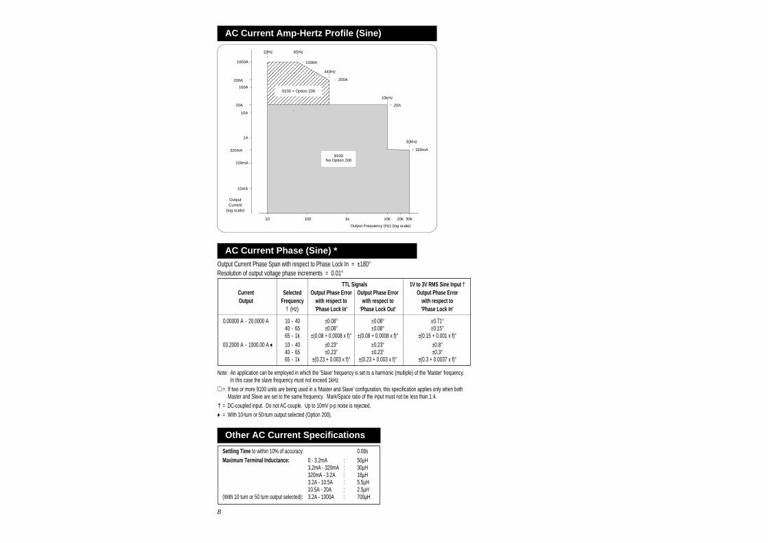
AC Current Amp-Hertz Profile (Sine)
AAAAAAAAAAAAAAAAAAAAAAAAAAAAAAAAAAA
Output Frequency (Hz) (log scale)
Output Current
(log scale)
10Hz
10kHz
30kHz
320mA
30k10 10k 20k
20A
320mA
20A
10mA
100mA
1A
10A
100A
1000A
1k100
1000A
65Hz
9100 + Option 200
440Hz
200A 200A
9100No Option 200
Other AC Current Specifications
Settling Time to within 10% of accuracy: 0.08sMaximum Terminal Inductance: 0 - 3.2mA : 50µH
3.2mA - 320mA : 30µH320mA - 3.2A : 18µH3.2A - 10.5A : 5.5µH10.5A - 20A : 2.5µH
(With 10 turn or 50 turn output selected): 3.2A - 1000A : 700µH
AC Current Phase (Sine) *Output Current Phase Span with respect to Phase Lock In = ±180°Resolution of output voltage phase increments = 0.01°
TTL Signals 1V to 3V RMS Sine Input †Current Selected Output Phase Error Output Phase Error Output Phase ErrorOutput Frequency with respect to with respect to with respect to
f (Hz) 'Phase Lock In' 'Phase Lock Out' 'Phase Lock In'
0.00000 A - 20.0000 A 10 - 40 ±0.08° ±0.08° ±0.71°40 - 65 ±0.08° ±0.08° ±0.15°65 - 1k ±(0.08 + 0.0008 x f)° ±(0.08 + 0.0008 x f)° ±(0.15 + 0.001 x f)°
03.2000 A - 1000.00 A ♠ 10 - 40 ±0.23° ±0.23° ±0.8°40 - 65 ±0.23° ±0.23° ±0.3°65 - 1k ±(0.23 + 0.003 x f)° ±(0.23 + 0.003 x f)° ±(0.3 + 0.0037 x f)°
Note: An application can be employed in which the 'Slave' frequency is set to a harmonic (multiple) of the 'Master' frequency.In this case the slave frequency must not exceed 1kHz.
∗ = If two or more 9100 units are being used in a 'Master and Slave' configuration, this specification applies only when bothMaster and Slave are set to the same frequency. Mark/Space ratio of the input must not be less than 1:4.
† = DC-coupled input. Do not AC-couple. Up to 10mV p-p noise is rejected.♠ = With 10-turn or 50-turn output selected (Option 200).
9
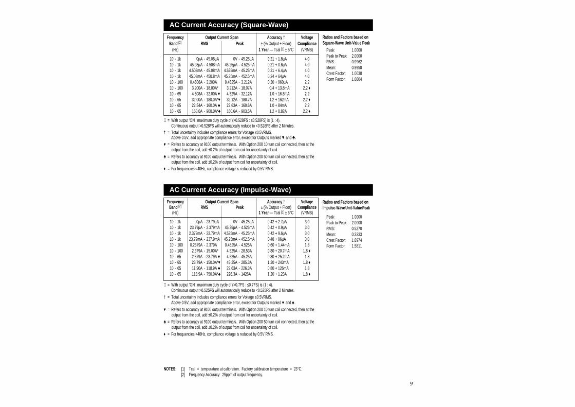
Frequency Output Current Span Accuracy † VoltageBand [2] RMS Peak ± (% Output + Floor) Compliance
(Hz) 1 Year — Tcal [1] ± 5°C (VRMS)
10 - 1k 0µA - 45.08µA 0V - 45.25µA 0.21 + 1.8µA 4.010 - 1k 45.08µA - 4.508mA 45.25µA - 4.525mA 0.21 + 0.6µA 4.010 - 1k 4.508mA - 45.08mA 4.525mA - 45.25mA 0.21 + 6.4µA 4.010 - 1k 45.08mA - 450.8mA 45.25mA - 452.5mA 0.24 + 64µA 4.010 - 100 0.4508A - 3.200A 0.4525A - 3.212A 0.30 + 960µA 2.210 - 100 3.200A - 18.00A* 3.212A - 18.07A 0.4 + 13.8mA 2.2 ♦10 - 65 4.508A - 32.00A ♥ 4.525A - 32.12A 1.0 + 16.8mA 2.210 - 65 32.00A - 180.0A*♥ 32.12A - 180.7A 1.2 + 162mA 2.2 ♦10 - 65 22.54A - 160.0A ♣ 22.63A - 160.6A 1.0 + 84mA 2.210 - 65 160.0A - 900.0A*♣ 160.6A - 903.5A 1.2 + 0.82A 2.2 ♦
AC Current Accuracy (Square-Wave)
Ratios and Factors based onSquare-Wave Unit-Value Peak
Peak: 1.0000Peak to Peak: 2.0000RMS: 0.9962Mean: 0.9958Crest Factor: 1.0038Form Factor: 1.0004
∗ = With output 'ON', maximum duty cycle of (>0.528FS : ≤0.528FS) is (1 : 4).Continuous output >0.528FS will automatically reduce to <0.528FS after 2 Minutes.
† = Total uncertainty includes compliance errors for Voltage ≤0.5VRMS.Above 0.5V, add appropriate compliance error, except for Outputs marked ♥ and ♣ .
♥ = Refers to accuracy at 9100 output terminals. With Option 200 10 turn coil connected, then at theoutput from the coil, add ±0.2% of output from coil for uncertainty of coil.
♣ = Refers to accuracy at 9100 output terminals. With Option 200 50 turn coil connected, then at theoutput from the coil, add ±0.2% of output from coil for uncertainty of coil.
♦ = For frequencies <40Hz, compliance voltage is reduced by 0.5V RMS.
AC Current Accuracy (Impulse-Wave)
Frequency Output Current Span Accuracy † VoltageBand [2] RMS Peak ± (% Output + Floor) Compliance
(Hz) 1 Year — Tcal [1] ± 5°C (VRMS)
10 - 1k 0µA - 23.79µA 0V - 45.25µA 0.42 + 2.7µA 3.010 - 1k 23.79µA - 2.379mA 45.25µA - 4.525mA 0.42 + 0.9µA 3.010 - 1k 2.379mA - 23.79mA 4.525mA - 45.25mA 0.42 + 9.6µA 3.010 - 1k 23.79mA - 237.9mA 45.25mA - 452.5mA 0.48 + 96µA 3.010 - 100 0.2379A - 2.379A 0.4525A - 4.525A 0.60 + 1.44mA 1.810 - 100 2.379A - 15.00A* 4.525A - 28.53A 0.80 + 20.7mA 1.8 ♦10 - 65 2.379A - 23.79A ♥ 4.525A - 45.25A 0.80 + 25.2mA 1.810 - 65 23.79A - 150.0A*♥ 45.25A - 285.3A 1.20 + 243mA 1.8 ♦10 - 65 11.90A - 118.9A ♣ 22.63A - 226.3A 0.80 + 126mA 1.810 - 65 118.9A - 750.0A*♣ 226.3A - 1426A 1.20 + 1.23A 1.8 ♦
Ratios and Factors based onImpulse-Wave Unit-Value Peak
Peak: 1.0000Peak to Peak: 2.0000RMS: 0.5270Mean: 0.3333Crest Factor: 1.8974Form Factor: 1.5811
∗ = With output 'ON', maximum duty cycle of (>0.7FS : ≤0.7FS) is (1 : 4).Continuous output >0.525FS will automatically reduce to <0.525FS after 2 Minutes.
† = Total uncertainty includes compliance errors for Voltage ≤0.5VRMS.Above 0.5V, add appropriate compliance error, except for Outputs marked ♥ and ♣ .
♥ = Refers to accuracy at 9100 output terminals. With Option 200 10 turn coil connected, then at theoutput from the coil, add ±0.2% of output from coil for uncertainty of coil.
♣ = Refers to accuracy at 9100 output terminals. With Option 200 50 turn coil connected, then at theoutput from the coil, add ±0.2% of output from coil for uncertainty of coil.
♦ = For frequencies <40Hz, compliance voltage is reduced by 0.5V RMS.
NOTES: [1] Tcal = temperature at calibration. Factory calibration temperature = 23°C.[2] Frequency Accuracy: 25ppm of output frequency.
10
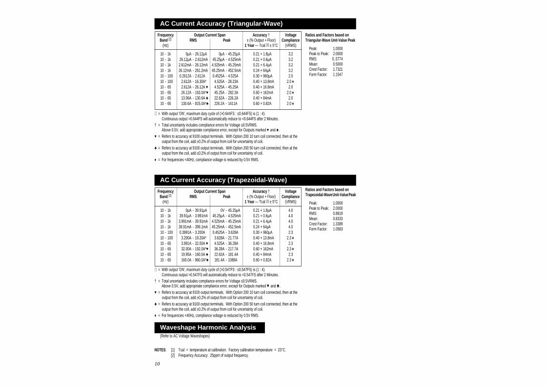
AC Current Accuracy (Triangular-Wave)
Frequency Output Current Span Accuracy † VoltageBand [2] RMS Peak ± (% Output + Floor) Compliance
(Hz) 1 Year — Tcal [1] ± 5°C (VRMS)
10 - 1k 0µA - 26.12µA 0µA - 45.25µA 0.21 + 1.8µA 3.210 - 1k 26.12µA - 2.612mA 45.25µA - 4.525mA 0.21 + 0.6µA 3.210 - 1k 2.612mA - 26.12mA 4.525mA - 45.25mA 0.21 + 6.4µA 3.210 - 1k 26.12mA - 261.2mA 45.25mA - 452.5mA 0.24 + 64µA 3.210 - 100 0.2612A - 2.612A 0.4525A - 4.525A 0.30 + 960µA 2.010 - 100 2.612A - 16.30A* 4.525A - 28.23A 0.40 + 13.8mA 2.0 ♦10 - 65 2.612A - 26.12A ♥ 4.525A - 45.25A 0.40 + 16.8mA 2.010 - 65 26.12A - 163.0A*♥ 45.25A - 282.3A 0.60 + 162mA 2.0 ♦10 - 65 13.06A - 130.6A ♣ 22.62A - 226.2A 0.40 + 84mA 2.010 - 65 130.6A - 815.0A*♣ 226.2A - 1411A 0.60 + 0.82A 2.0 ♦
Ratios and Factors based onTriangular-Wave Unit-Value Peak
Peak: 1.0000Peak to Peak: 2.0000RMS: 0..5774Mean: 0.5000Crest Factor: 1.7321Form Factor: 1.1547
∗ = With output 'ON', maximum duty cycle of (>0.644FS : ≤0.644FS) is (1 : 4).Continuous output >0.644FS will automatically reduce to <0.644FS after 2 Minutes.
† = Total uncertainty includes compliance errors for Voltage ≤0.5VRMS.Above 0.5V, add appropriate compliance error, except for Outputs marked ♥ and ♣.
♥ = Refers to accuracy at 9100 output terminals. With Option 200 10 turn coil connected, then at theoutput from the coil, add ±0.2% of output from coil for uncertainty of coil.
♣ = Refers to accuracy at 9100 output terminals. With Option 200 50 turn coil connected, then at theoutput from the coil, add ±0.2% of output from coil for uncertainty of coil.
♦ = For frequencies <40Hz, compliance voltage is reduced by 0.5V RMS.
AC Current Accuracy (Trapezoidal-Wave)
Frequency Output Current Span Accuracy † VoltageBand [2] RMS Peak ± (% Output + Floor) Compliance
(Hz) 1 Year — Tcal [1] ± 5°C (VRMS)
10 - 1k 0µA - 39.91µA 0V - 45.25µA 0.21 + 1.8µA 4.010 - 1k 39.91µA - 3.991mA 45.25µA - 4.525mA 0.21 + 0.6µA 4.010 - 1k 3.991mA - 39.91mA 4.525mA - 45.25mA 0.21 + 6.4µA 4.010 - 1k 39.91mA - 399.1mA 45.25mA - 452.5mA 0.24 + 64µA 4.010 - 100 0.3991A - 3.200A 0.4525A - 3.628A 0.30 + 960µA 2.310 - 100 3.200A - 19.20A* 3.628A - 21.77A 0.40 + 13.8mA 2.3 ♦10 - 65 3.991A - 32.00A ♥ 4.525A - 36.28A 0.40 + 16.8mA 2.310 - 65 32.00A - 192.0A*♥ 36.28A - 217.7A 0.60 + 162mA 2.3 ♦10 - 65 19.95A - 160.0A ♣ 22.62A - 181.4A 0.40 + 84mA 2.310 - 65 160.0A - 960.0A*♣ 181.4A - 1088A 0.60 + 0.82A 2.3 ♦
Ratios and Factors based onTrapezoidal-Wave Unit-Value Peak
Peak: 1.0000Peak to Peak: 2.0000RMS: 0.8819Mean: 0.8333Crest Factor: 1.3389Form Factor: 1.0583
∗ = With output 'ON', maximum duty cycle of (>0.547FS : ≤0.547FS) is (1 : 4).Continuous output >0.547FS will automatically reduce to <0.547FS after 2 Minutes.
† = Total uncertainty includes compliance errors for Voltage ≤0.5VRMS.Above 0.5V, add appropriate compliance error, except for Outputs marked ♥ and ♣ .
♥ = Refers to accuracy at 9100 output terminals. With Option 200 10 turn coil connected, then at theoutput from the coil, add ±0.2% of output from coil for uncertainty of coil.
♣ = Refers to accuracy at 9100 output terminals. With Option 200 50 turn coil connected, then at theoutput from the coil, add ±0.2% of output from coil for uncertainty of coil.
♦ = For frequencies <40Hz, compliance voltage is reduced by 0.5V RMS.
Waveshape Harmonic Analysis(Refer to AC Voltage Waveshapes)
NOTES: [1] Tcal = temperature at calibration. Factory calibration temperature = 23°C.[2] Frequency Accuracy: 25ppm of output frequency.
11
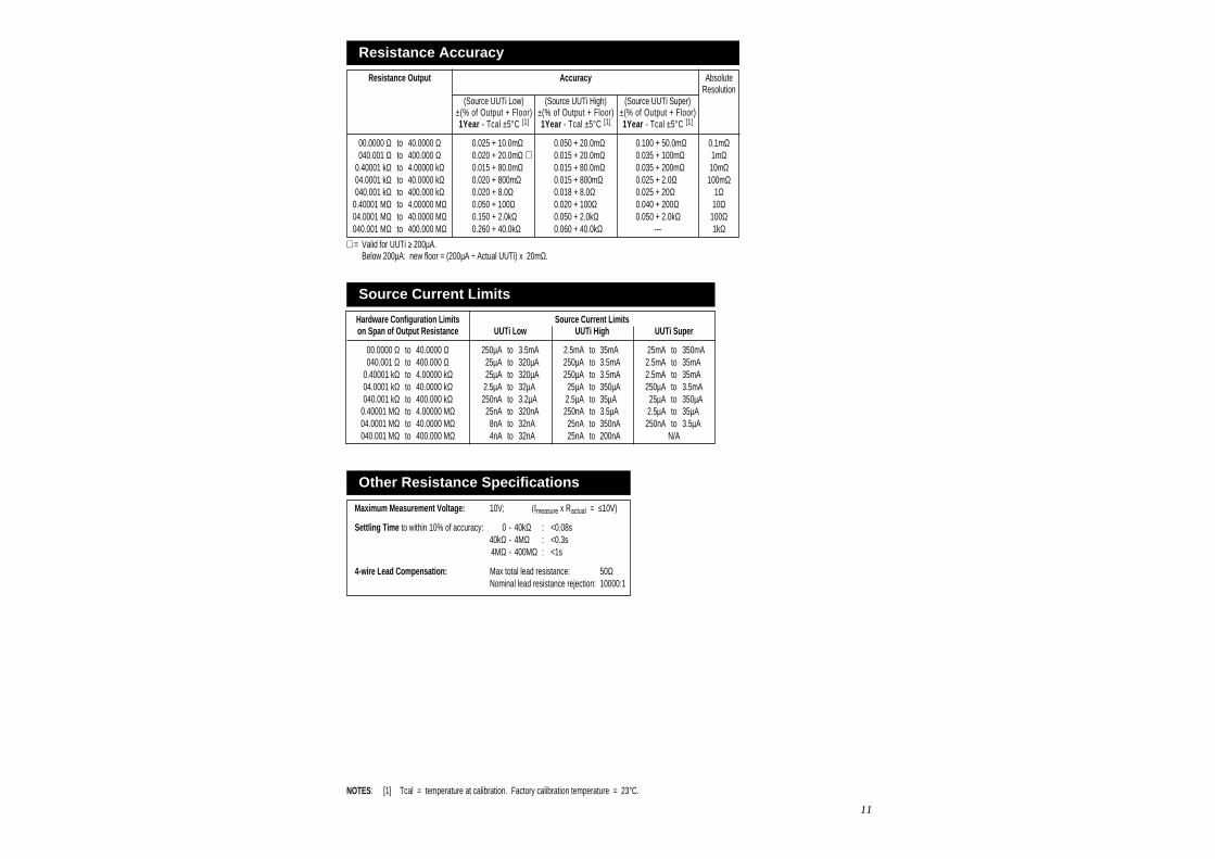
Source Current Limits
Hardware Configuration Limits Source Current Limitson Span of Output Resistance UUTi Low UUTi High UUTi Super
00.0000 Ω to 40.0000 Ω 250µA to 3.5mA 2.5mA to 35mA 25mA to 350mA040.001 Ω to 400.000 Ω 25µA to 320µA 250µA to 3.5mA 2.5mA to 35mA
0.40001 kΩ to 4.00000 kΩ 25µA to 320µA 250µA to 3.5mA 2.5mA to 35mA04.0001 kΩ to 40.0000 kΩ 2.5µA to 32µA 25µA to 350µA 250µA to 3.5mA040.001 kΩ to 400.000 kΩ 250nA to 3.2µA 2.5µA to 35µA 25µA to 350µA
0.40001 MΩ to 4.00000 MΩ 25nA to 320nA 250nA to 3.5µA 2.5µA to 35µA04.0001 MΩ to 40.0000 MΩ 8nA to 32nA 25nA to 350nA 250nA to 3.5µA040.001 MΩ to 400.000 MΩ 4nA to 32nA 25nA to 200nA N/A
Other Resistance Specifications
Maximum Measurement Voltage: 10V; (Imeasure x Ractual = ≤10V)
Settling Time to within 10% of accuracy: 0 - 40kΩ : <0.08s40kΩ - 4MΩ : <0.3s4MΩ - 400MΩ : <1s
4-wire Lead Compensation: Max total lead resistance: 50ΩNominal lead resistance rejection: 10000:1
NOTES: [1] Tcal = temperature at calibration. Factory calibration temperature = 23°C.
Resistance Accuracy
Resistance Output Accuracy AbsoluteResolution
(Source UUTi Low) (Source UUTi High) (Source UUTi Super)±(% of Output + Floor) ±(% of Output + Floor) ±(% of Output + Floor)1Year - Tcal ±5°C [1] 1Year - Tcal ±5°C [1] 1Year - Tcal ±5°C [1]
00.0000 Ω to 40.0000 Ω 0.025 + 10.0mΩ 0.050 + 20.0mΩ 0.100 + 50.0mΩ 0.1mΩ040.001 Ω to 400.000 Ω 0.020 + 20.0mΩ ∗ 0.015 + 20.0mΩ 0.035 + 100mΩ 1mΩ
0.40001 kΩ to 4.00000 kΩ 0.015 + 80.0mΩ 0.015 + 80.0mΩ 0.035 + 200mΩ 10mΩ04.0001 kΩ to 40.0000 kΩ 0.020 + 800mΩ 0.015 + 800mΩ 0.025 + 2.0Ω 100mΩ040.001 kΩ to 400.000 kΩ 0.020 + 8.0Ω 0.018 + 8.0Ω 0.025 + 20Ω 1Ω
0.40001 MΩ to 4.00000 MΩ 0.050 + 100Ω 0.020 + 100Ω 0.040 + 200Ω 10Ω04.0001 MΩ to 40.0000 MΩ 0.150 + 2.0kΩ 0.050 + 2.0kΩ 0.050 + 2.0kΩ 100Ω040.001 MΩ to 400.000 MΩ 0.260 + 40.0kΩ 0.060 + 40.0kΩ --- 1kΩ
∗ = Valid for UUTi ≥ 200µA.Below 200µA: new floor = (200µA ÷ Actual UUTi) x 20mΩ.
12
Ω
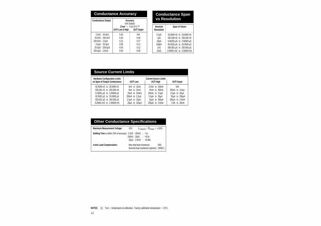
Conductance Accuracy
Conductance Output Accuracy±(% Output)
1Year — Tcal ±5°C [1]
UUTi Low & High UUTi Super
2.5nS - 25.0nS 0.40 N/A25.0nS - 250.0nS 0.20 0.45
250.0nS - 2.5µS 0.12 0.272.5µS - 25.0µS 0.05 0.12
25.0µS - 250.0µS 0.05 0.12250.0µS - 2.5mS 0.04 0.09
Absolute Span of ValuesResolution
0.1pS 02.5000 nS to 25.0000 nS1pS 002.500 nS to 250.000 nS
10pS 0.00250 µS to 2.50000 µS100pS 00.0025 µS to 25.0000 µS
1nS 000.002 µS to 250.000 µS10nS 0.00001 mS to 2.50000 mS
Conductance Spanvs Resolution
Source Current Limits
Hardware Configuration Limits Current Source Limitson Span of Output Conductance UUTi Low UUTi High UUTi Super
02.5000 nS to 25.0000 nS 4nA to 32nA 2.5nA to 200nA N/A025.001 nS to 250.000 nS 8nA to 32nA 25nA to 350nA 250nA to 3.5µA0.25001 µS to 2.50000 µS 25nA to 320nA 250nA to 3.5µA 2.5µA to 35µA02.5001 µS to 25.0000 µS 250nA to 3.2µA 2.5µA to 35µA 25µA to 350µA025.001 µS to 250.000 µS 2.5µA to 32µA 25µA to 350µA 250µA to 3.5mA0.25001 mS to 2.50000 mS 25µA to 320µA 250µA to 3.5mA 2.5A to 35mA
Other Conductance Specifications
Maximum Measurement Voltage: 10V; (I measure ÷ actual = ≤10V)
Settling Time to within 10% of accuracy: 2.5nS - 250nS : <1s250nS - 25µS : <0.3s25µS - 2.5mS : <0.08s
4-wire Lead Compensation: Max total lead resistance: 50ΩNominal lead resistance rejection: 10000:1
NOTES: [1] Tcal = temperature at calibration. Factory calibration temperature = 23°C.
13
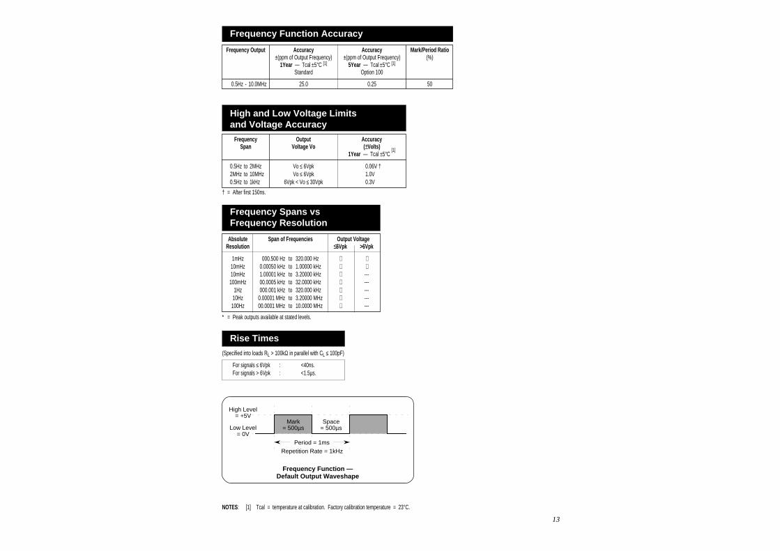
Frequency Function Accuracy
Frequency Output Accuracy Accuracy Mark/Period Ratio±(ppm of Output Frequency) ±(ppm of Output Frequency) (%)
1Year — Tcal ±5°C [1] 5Year — Tcal ±5°C [1]
Standard Option 100
0.5Hz - 10.0MHz 25.0 0.25 50
Frequency Output AccuracySpan Voltage Vo (±Volts)
1Year — Tcal ±5°C [1]
0.5Hz to 2MHz Vo ≤ 6Vpk 0.06V †2MHz to 10MHz Vo ≤ 6Vpk 1.0V0.5Hz to 1kHz 6Vpk < Vo ≤ 30Vpk 0.3V
High and Low Voltage Limitsand Voltage Accuracy
Frequency Spans vsFrequency Resolution
Absolute Span of Frequencies Output VoltageResolution ≤6Vpk >6Vpk
1mHz 000.500 Hz to 320.000 Hz ∗ ∗10mHz 0.00050 kHz to 1.00000 kHz ∗ ∗10mHz 1.00001 kHz to 3.20000 kHz ∗ ---100mHz 00.0005 kHz to 32.0000 kHz ∗ ---
1Hz 000.001 kHz to 320.000 kHz ∗ ---10Hz 0.00001 MHz to 3.20000 MHz ∗ ---100Hz 00.0001 MHz to 10.0000 MHz ∗ ---
* = Peak outputs available at stated levels.
For signals ≤ 6Vpk : <40ns.For signals > 6Vpk : <1.5µs.
Rise Times
(Specified into loads RL > 100kΩ in parallel with CL ≤ 100pF)
Mark= 500µs
Space= 500µs
Period = 1msRepetition Rate = 1kHz
High Level= +5V
Low Level= 0V
NOTES: [1] Tcal = temperature at calibration. Factory calibration temperature = 23°C.
Frequency Function —Default Output Waveshape
† = After first 150ns.
14
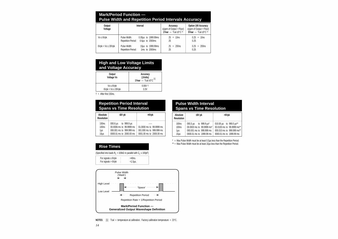
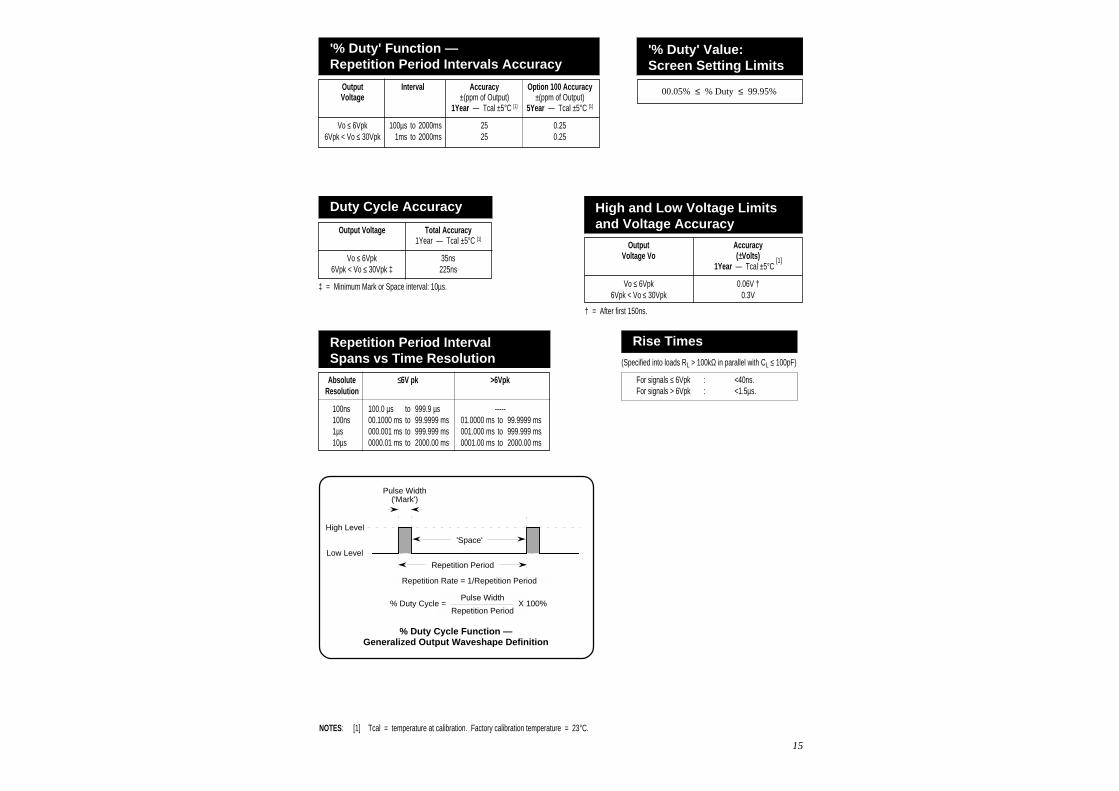
Mark/Period Function —Pulse Width and Repetition Period Intervals Accuracy
Output Interval Accuracy Option 100 AccuracyVoltage ±(ppm of Output + Floor) ±(ppm of Output + Floor)
1Year — Tcal ±5°C [1] 5Year — Tcal ±5°C [1]
Vo ≤ 6Vpk Pulse Width: 0.30µs to 1999.99ms 25 + 10ns 0.25 + 10nsRepetition Period: 0.6µs to 2000ms 25 0.25
6Vpk < Vo ≤ 30Vpk Pulse Width: 10µs to 1999.99ms 25 + 200ns 0.25 + 200nsRepetition Period: 1ms to 2000ms 25 0.25
Output AccuracyVoltage Vo (±Volts)
1Year — Tcal ±5°C [1]
Vo ≤ 6Vpk 0.06V †6Vpk < Vo ≤ 30Vpk 0.3V
High and Low Voltage Limitsand Voltage Accuracy
NOTES: [1] Tcal = temperature at calibration. Factory calibration temperature = 23°C.
Pulse Width IntervalSpans vs Time Resolution
Absolute ≤6V pk >6VpkResolution
100ns 000.3 µs to 999.9 µs* 010.00 µs to 990.0 µs**100ns 00.0003 ms to 99.9999 ms* 00.0100 ms to 99.9999 ms**1µs 000.001 ms to 999.999 ms 000.010 ms to 999.999 ms**10µs 0000.01 ms to 1999.99 ms 0000.01 ms to 1999.99 ms
* = Max Pulse Width must be at least 0.3µs less than the Repetition Period.** = Max Pulse Width must be at least 10µs less than the Repetition Period.
Repetition Period IntervalSpans vs Time Resolution
Absolute ≤6V pk >6VpkResolution
100ns 000.6 µs to 999.9 µs -----100ns 00.0006 ms to 99.9999 ms 01.0000 ms to 99.9999 ms1µs 000.001 ms to 999.999 ms 001.000 ms to 999.999 ms10µs 0000.01 ms to 2000.00 ms 0001.00 ms to 2000.00 ms
For signals ≤ 6Vpk : <40ns.For signals > 6Vpk : <1.5µs.
Rise Times
(Specified into loads RL > 100kΩ in parallel with CL ≤ 100pF)
Pulse Width('Mark')
Repetition Period
Repetition Rate = 1/Repetition Period
High Level
Low Level
'Space'
Mark/Period Function —Generalized Output Waveshape Definition
† = After first 150ns.
15
NOTES: [1] Tcal = temperature at calibration. Factory calibration temperature = 23°C.
'% Duty' Function —Repetition Period Intervals Accuracy
'% Duty' Value:Screen Setting Limits
00.05% ≤ % Duty ≤ 99.95%Output Interval Accuracy Option 100 AccuracyVoltage ±(ppm of Output) ±(ppm of Output)
1Year — Tcal ±5°C [1] 5Year — Tcal ±5°C [1]
Vo ≤ 6Vpk 100µs to 2000ms 25 0.256Vpk < Vo ≤ 30Vpk 1ms to 2000ms 25 0.25
Duty Cycle Accuracy
Output Voltage Total Accuracy1Year — Tcal ±5°C [1]
Vo ≤ 6Vpk 35ns6Vpk < Vo ≤ 30Vpk ‡ 225ns
‡ = Minimum Mark or Space interval: 10µs.
Output AccuracyVoltage Vo (±Volts)
1Year — Tcal ±5°C [1]
Vo ≤ 6Vpk 0.06V †6Vpk < Vo ≤ 30Vpk 0.3V
High and Low Voltage Limitsand Voltage Accuracy
Repetition Period IntervalSpans vs Time Resolution
Absolute ≤6V pk >6VpkResolution
100ns 100.0 µs to 999.9 µs -----100ns 00.1000 ms to 99.9999 ms 01.0000 ms to 99.9999 ms1µs 000.001 ms to 999.999 ms 001.000 ms to 999.999 ms10µs 0000.01 ms to 2000.00 ms 0001.00 ms to 2000.00 ms
For signals ≤ 6Vpk : <40ns.For signals > 6Vpk : <1.5µs.
Rise Times
(Specified into loads RL > 100kΩ in parallel with CL ≤ 100pF)
Pulse Width('Mark')
Repetition Period
Repetition Rate = 1/Repetition Period
High Level
Low Level
'Space'
Pulse Width
Repetition Period% Duty Cycle = X 100%
% Duty Cycle Function —Generalized Output Waveshape Definition
† = After first 150ns.
16
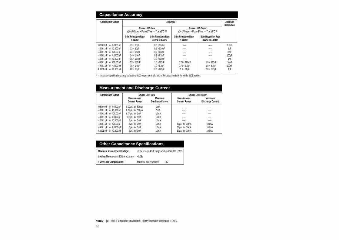
Capacitance Accuracy
Capacitance Output Accuracy * AbsoluteResolution
Source UUTi Low Source UUTi Super±(% of Output + Floor) 1Year — Tcal ±5°C [1] ±(% of Output + Floor) 1Year — Tcal ±5°C [1]
Stim Repetition Rate Stim Repetition Rate Stim Repetition Rate Stim Repetition Rate≤ 350Hz 350Hz to 1.5kHz ≤ 350Hz 350Hz to 1.5kHz
0.5000 nF to 4.0000 nF 0.3 + 15pF 0.6 +30.0pF ----- ----- 0.1pF4.0001 nF to 40.000 nF 0.3 + 30pF 0.6 +60.0pF ----- ----- 1pF40.001 nF to 400.00 nF 0.3 + 160pF 0.6 +320pF ----- ----- 10pF400.01 nF to 4.0000 µF 0.4 + 1.6nF 0.8 +3.2nF ----- ----- 100pF4.0001 µF to 40.000 µF 0.5 + 16.0nF 1.0 +32.0nF ----- ----- 1nF40.001 µF to 400.00 µF 0.5 + 160nF 1.0 +320nF 0.75 + 160nF 1.0 + 320nF 10nF400.01 µF to 4.0000 mF 0.5 + 1.6µF 1.0 +3.2µF 0.75 + 1.6µF 1.0 + 3.2µF 100nF4.0001 mF to 40.000 mF 1.0 + 60µF 2.0 +120µF 1.0 + 60µF 2.0 + 120µF 1µF
* = Accuracy specifications apply both at the 9100 output terminals, and at the output leads of the Model 9105 leadset.
Measurement and Discharge Current
Capacitance Output Source UUTi Low Source UUTi SuperMeasurement Maximum Measurement MaximumCurrent Range Discharge Current Current Range Discharge Current
0.5000 nF to 4.0000 nF 0.02µA to 500µA 1mA ----- -----4.0001 nF to 40.000 nF 0.02µA to 500µA 5mA ----- -----40.001 nF to 400.00 nF 0.04µA to 1mA 10mA ----- -----400.01 nF to 4.0000 µF 0.5µA to 1mA 10mA ----- -----4.0001 µF to 40.000 µF 5µA to 3mA 10mA ----- -----40.001 µF to 400.00 µF 5µA to 3mA 10mA 50µA to 30mA 100mA400.01 µF to 4.0000 mF 5µA to 3mA 10mA 50µA to 30mA 100mA4.0001 mF to 40.000 mF 5µA to 3mA 10mA 50µA to 30mA 100mA
Other Capacitance Specifications
Maximum Measurement Voltage: ±3.5V (except 40µF range which is limited to ±2.5V)
Settling Time to within 10% of accuracy: <0.08s
4-wire Lead Compensation: Max total lead resistance: 10Ω
NOTES: [1] Tcal = temperature at calibration. Factory calibration temperature = 23°C.
17
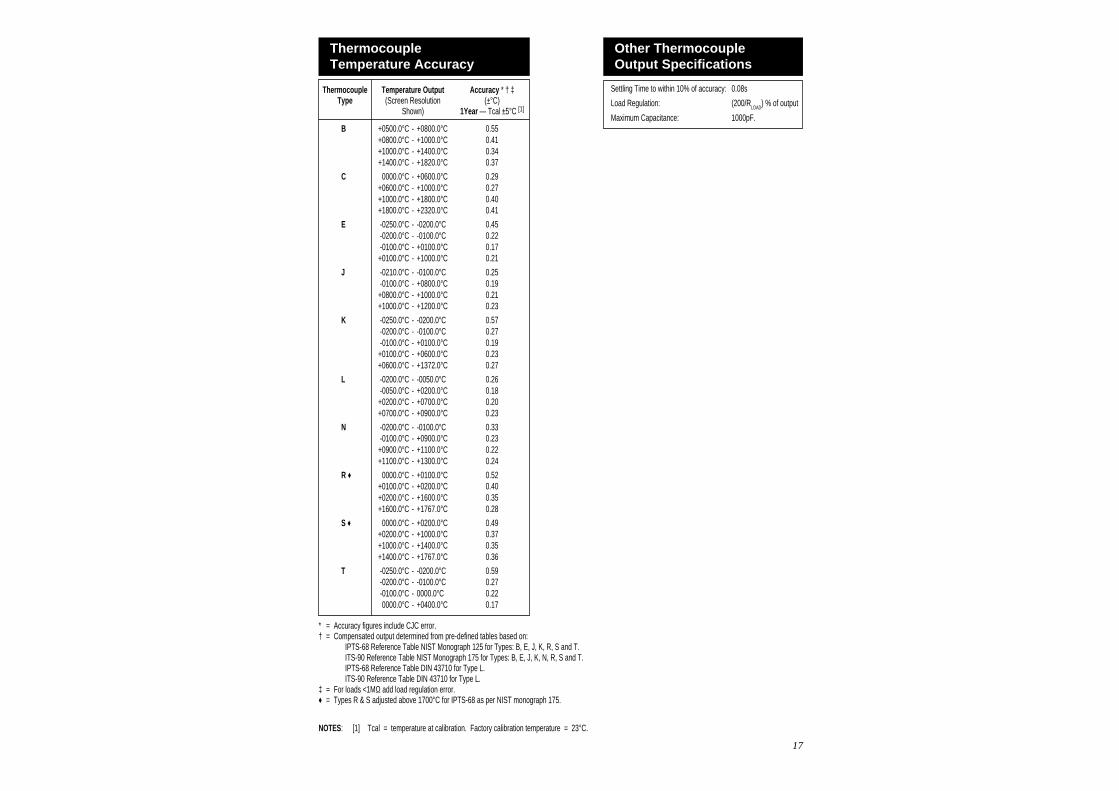
ThermocoupleTemperature Accuracy
Thermocouple Temperature Output Accuracy * † ‡Type (Screen Resolution (±°C)
Shown) 1Year — Tcal ±5°C [1]
B +0500.0°C - +0800.0°C 0.55+0800.0°C - +1000.0°C 0.41+1000.0°C - +1400.0°C 0.34+1400.0°C - +1820.0°C 0.37
C 0000.0°C - +0600.0°C 0.29+0600.0°C - +1000.0°C 0.27+1000.0°C - +1800.0°C 0.40+1800.0°C - +2320.0°C 0.41
E -0250.0°C - -0200.0°C 0.45-0200.0°C - -0100.0°C 0.22-0100.0°C - +0100.0°C 0.17+0100.0°C - +1000.0°C 0.21
J -0210.0°C - -0100.0°C 0.25-0100.0°C - +0800.0°C 0.19+0800.0°C - +1000.0°C 0.21+1000.0°C - +1200.0°C 0.23
K -0250.0°C - -0200.0°C 0.57-0200.0°C - -0100.0°C 0.27-0100.0°C - +0100.0°C 0.19+0100.0°C - +0600.0°C 0.23+0600.0°C - +1372.0°C 0.27
L -0200.0°C - -0050.0°C 0.26-0050.0°C - +0200.0°C 0.18+0200.0°C - +0700.0°C 0.20+0700.0°C - +0900.0°C 0.23
N -0200.0°C - -0100.0°C 0.33-0100.0°C - +0900.0°C 0.23+0900.0°C - +1100.0°C 0.22+1100.0°C - +1300.0°C 0.24
R ♦ 0000.0°C - +0100.0°C 0.52+0100.0°C - +0200.0°C 0.40+0200.0°C - +1600.0°C 0.35+1600.0°C - +1767.0°C 0.28
S ♦ 0000.0°C - +0200.0°C 0.49+0200.0°C - +1000.0°C 0.37+1000.0°C - +1400.0°C 0.35+1400.0°C - +1767.0°C 0.36
T -0250.0°C - -0200.0°C 0.59-0200.0°C - -0100.0°C 0.27-0100.0°C - 0000.0°C 0.220000.0°C - +0400.0°C 0.17
* = Accuracy figures include CJC error.† = Compensated output determined from pre-defined tables based on:
IPTS-68 Reference Table NIST Monograph 125 for Types: B, E, J, K, R, S and T.ITS-90 Reference Table NIST Monograph 175 for Types: B, E, J, K, N, R, S and T.IPTS-68 Reference Table DIN 43710 for Type L.ITS-90 Reference Table DIN 43710 for Type L.
‡ = For loads <1MΩ add load regulation error.♦ = Types R & S adjusted above 1700°C for IPTS-68 as per NIST monograph 175.
Other ThermocoupleOutput Specifications
Settling Time to within 10% of accuracy: 0.08s
Load Regulation: (200/RLOAD
) % of output
Maximum Capacitance: 1000pF.
NOTES: [1] Tcal = temperature at calibration. Factory calibration temperature = 23°C.
18
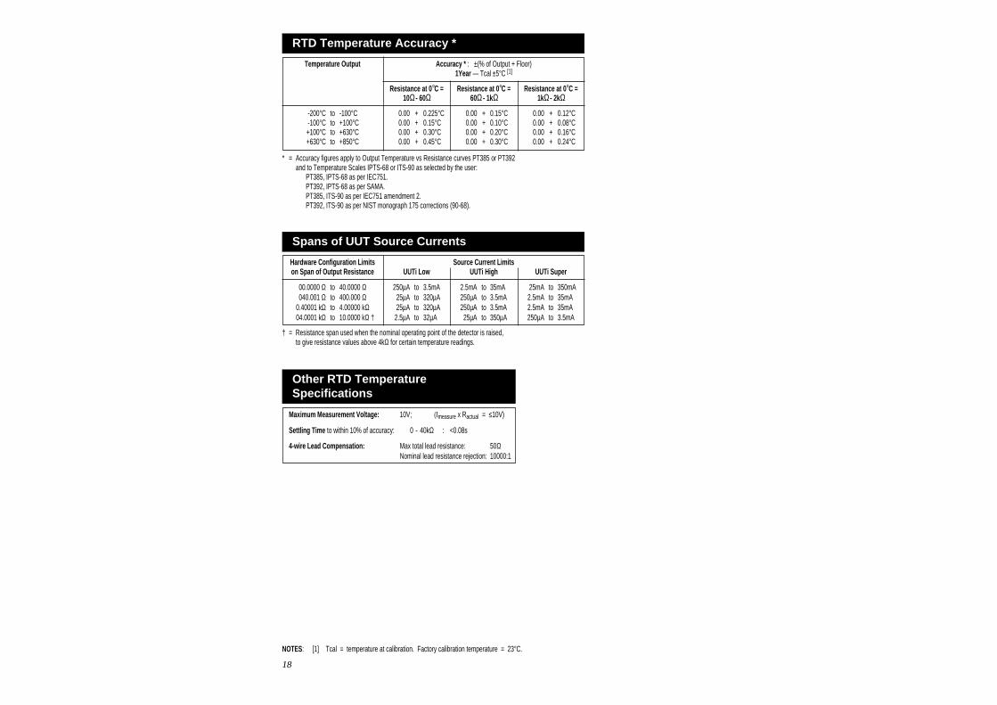
RTD Temperature Accuracy *
Temperature Output Accuracy * : ±(% of Output + Floor)1Year — Tcal ±5°C [1]
Resistance at 0°C = Resistance at 0°C = Resistance at 0°C =10Ω - 60Ω 60Ω - 1kΩ 1kΩ - 2kΩ
-200°C to -100°C 0.00 + 0.225°C 0.00 + 0.15°C 0.00 + 0.12°C-100°C to +100°C 0.00 + 0.15°C 0.00 + 0.10°C 0.00 + 0.08°C+100°C to +630°C 0.00 + 0.30°C 0.00 + 0.20°C 0.00 + 0.16°C+630°C to +850°C 0.00 + 0.45°C 0.00 + 0.30°C 0.00 + 0.24°C
* = Accuracy figures apply to Output Temperature vs Resistance curves PT385 or PT392and to Temperature Scales IPTS-68 or ITS-90 as selected by the user:
PT385, IPTS-68 as per IEC751.PT392, IPTS-68 as per SAMA.PT385, ITS-90 as per IEC751 amendment 2.PT392, ITS-90 as per NIST monograph 175 corrections (90-68).
Spans of UUT Source Currents
Hardware Configuration Limits Source Current Limitson Span of Output Resistance UUTi Low UUTi High UUTi Super
00.0000 Ω to 40.0000 Ω 250µA to 3.5mA 2.5mA to 35mA 25mA to 350mA040.001 Ω to 400.000 Ω 25µA to 320µA 250µA to 3.5mA 2.5mA to 35mA
0.40001 kΩ to 4.00000 kΩ 25µA to 320µA 250µA to 3.5mA 2.5mA to 35mA04.0001 kΩ to 10.0000 kΩ † 2.5µA to 32µA 25µA to 350µA 250µA to 3.5mA
† = Resistance span used when the nominal operating point of the detector is raised,to give resistance values above 4kΩ for certain temperature readings.
NOTES: [1] Tcal = temperature at calibration. Factory calibration temperature = 23°C.
Other RTD TemperatureSpecifications
Maximum Measurement Voltage: 10V; (Imeasure x Ractual = ≤10V)
Settling Time to within 10% of accuracy: 0 - 40kΩ : <0.08s
4-wire Lead Compensation: Max total lead resistance: 50ΩNominal lead resistance rejection: 10000:1
19
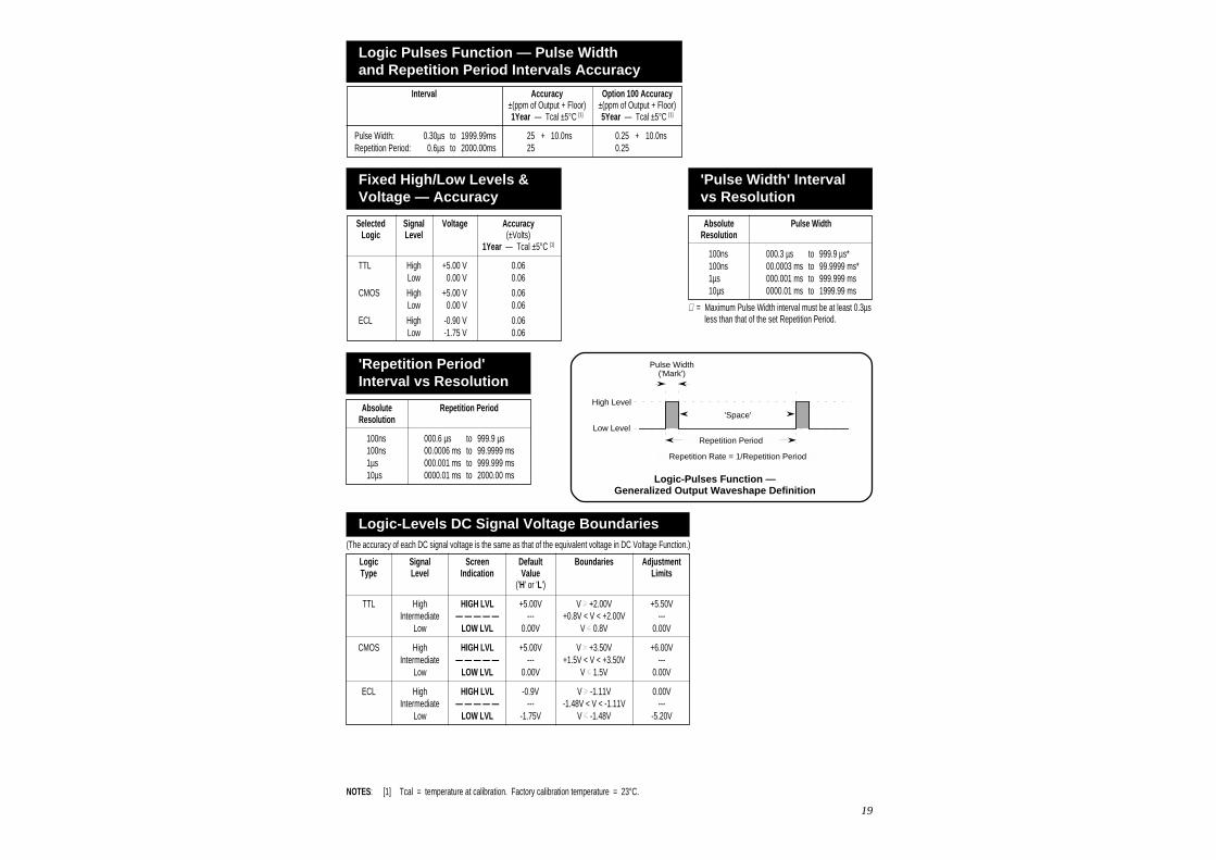
Logic Pulses Function — Pulse Widthand Repetition Period Intervals Accuracy
Interval Accuracy Option 100 Accuracy±(ppm of Output + Floor) ±(ppm of Output + Floor)1Year — Tcal ±5°C [1] 5Year — Tcal ±5°C [1]
Pulse Width: 0.30µs to 1999.99ms 25 + 10.0ns 0.25 + 10.0nsRepetition Period: 0.6µs to 2000.00ms 25 0.25
NOTES: [1] Tcal = temperature at calibration. Factory calibration temperature = 23°C.
Fixed High/Low Levels &Voltage — Accuracy
Selected Signal Voltage AccuracyLogic Level (±Volts)
1Year — Tcal ±5°C [1]
TTL High +5.00 V 0.06Low 0.00 V 0.06
CMOS High +5.00 V 0.06Low 0.00 V 0.06
ECL High -0.90 V 0.06Low -1.75 V 0.06
'Pulse Width' Intervalvs Resolution
Absolute Pulse WidthResolution
100ns 000.3 µs to 999.9 µs*100ns 00.0003 ms to 99.9999 ms*1µs 000.001 ms to 999.999 ms10µs 0000.01 ms to 1999.99 ms
∗ = Maximum Pulse Width interval must be at least 0.3µsless than that of the set Repetition Period.
Pulse Width('Mark')
Repetition Period
Repetition Rate = 1/Repetition Period
High Level
Low Level
'Space'
Logic-Pulses Function —Generalized Output Waveshape Definition
'Repetition Period'Interval vs Resolution
Absolute Repetition PeriodResolution
100ns 000.6 µs to 999.9 µs100ns 00.0006 ms to 99.9999 ms1µs 000.001 ms to 999.999 ms10µs 0000.01 ms to 2000.00 ms
Logic-Levels DC Signal Voltage Boundaries(The accuracy of each DC signal voltage is the same as that of the equivalent voltage in DC Voltage Function.)
Logic Signal Screen Default Boundaries AdjustmentType Level Indication Value Limits
('H' or 'L')
TTL High HIGH LVL +5.00V V +2.00V +5.50VIntermediate — — — — — --- +0.8V < V < +2.00V ---
Low LOW LVL 0.00V V 0.8V 0.00V
CMOS High HIGH LVL +5.00V V +3.50V +6.00VIntermediate — — — — — --- +1.5V < V < +3.50V ---
Low LOW LVL 0.00V V 1.5V 0.00V
ECL High HIGH LVL -0.9V V -1.11V 0.00VIntermediate — — — — — --- -1.48V < V < -1.11V ---
Low LOW LVL -1.75V V -1.48V -5.20V
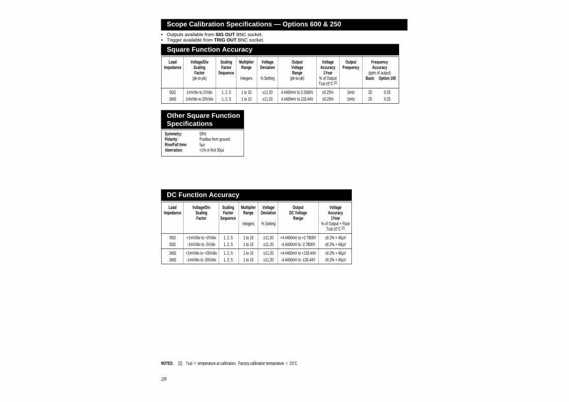
20
Load Voltage/Div Scaling Multiplier Voltage Output Voltage Output FrequencyImpedance Scaling Factor Range Deviation Voltage Accuracy Frequency Accuracy
Factor Sequence Range 1Year (ppm of output)(pk-to-pk) Integers % Setting (pk-to-pk) % of Output Basic Option 100
Tcal ±5°C [2]
50Ω 1mV/div to 2V/div 1, 2, 5 1 to 10 ±11.20 4.4400mV to 3.3360V ±0.25% 1kHz 25 0.251MΩ 1mV/div to 20V/div 1, 2, 5 1 to 10 ±11.20 4.4400mV to 133.44V ±0.25% 1kHz 25 0.25
Symmetry: 50%Polarity: Positive from groundRise/Fall time: 5µsAberration: <1% in first 30µs
Scope Calibration Specifications — Options 600 & 250• Outputs available from SIG OUT BNC socket.• Trigger available from TRIG OUT BNC socket.
Square Function Accuracy
Other Square FunctionSpecifications
DC Function Accuracy
Load Voltage/Div Scaling Multiplier Voltage Output VoltageImpedance Scaling Factor Range Deviation DC Voltage Accuracy
Factor Sequence Range 1YearIntegers % Setting % of Output + Floor
Tcal ±5°C [2]
50Ω +1mV/div to +2V/div 1, 2, 5 1 to 10 ±11.20 +4.4400mV to +2.7800V ±0.2% + 40µV50Ω -1mV/div to -2V/div 1, 2, 5 1 to 10 ±11.20 -4.4400mV to -2.7800V ±0.2% + 40µV
1MΩ +1mV/div to +20V/div 1, 2, 5 1 to 10 ±11.20 +4.4400mV to +133.44V ±0.2% + 40µV1MΩ -1mV/div to -20V/div 1, 2, 5 1 to 10 ±11.20 -4.4400mV to -133.44V ±0.2% + 40µV
NOTES: [2] Tcal = temperature at calibration. Factory calibration temperature = 23°C.
21
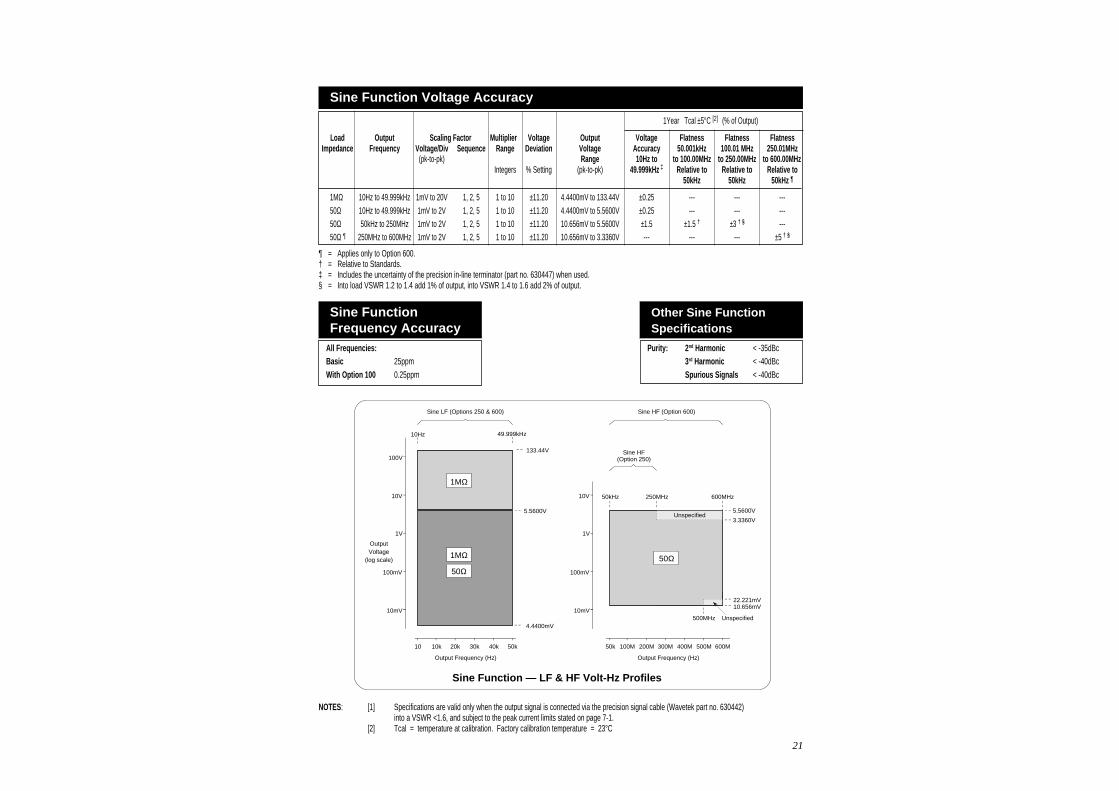
1Year Tcal ±5°C [2] (% of Output)
Load Output Scaling Factor Multiplier Voltage Output Voltage Flatness Flatness FlatnessImpedance Frequency Voltage/Div Sequence Range Deviation Voltage Accuracy 50.001kHz 100.01 MHz 250.01MHz
(pk-to-pk) Range 10Hz to to 100.00MHz to 250.00MHz to 600.00MHzIntegers % Setting (pk-to-pk) 49.999kHz ‡ Relative to Relative to Relative to
50kHz 50kHz 50kHz ¶
1MΩ 10Hz to 49.999kHz 1mV to 20V 1, 2, 5 1 to 10 ±11.20 4.4400mV to 133.44V ±0.25 --- --- ---50Ω 10Hz to 49.999kHz 1mV to 2V 1, 2, 5 1 to 10 ±11.20 4.4400mV to 5.5600V ±0.25 --- --- ---50Ω 50kHz to 250MHz 1mV to 2V 1, 2, 5 1 to 10 ±11.20 10.656mV to 5.5600V ±1.5 ±1.5 † ±3 † § ---50Ω ¶ 250MHz to 600MHz 1mV to 2V 1, 2, 5 1 to 10 ±11.20 10.656mV to 3.3360V --- --- --- ±5 † §
All Frequencies:Basic 25ppmWith Option 100 0.25ppm
Sine Function Voltage Accuracy
Sine FunctionFrequency Accuracy
Sine Function — LF & HF Volt-Hz Profiles
NOTES: [1] Specifications are valid only when the output signal is connected via the precision signal cable (Wavetek part no. 630442)into a VSWR <1.6, and subject to the peak current limits stated on page 7-1.
[2] Tcal = temperature at calibration. Factory calibration temperature = 23°C
¶ = Applies only to Option 600.† = Relative to Standards.‡ = Includes the uncertainty of the precision in-line terminator (part no. 630447) when used.§ = Into load VSWR 1.2 to 1.4 add 1% of output, into VSWR 1.4 to 1.6 add 2% of output.
Purity: 2nd Harmonic < -35dBc3rd Harmonic < -40dBcSpurious Signals < -40dBc
Other Sine FunctionSpecifications
Output Frequency (Hz)
600M
1V
10V
10mV
100mV
50kHz 250MHz
5.5600V
10.656mV
50Ω
3.3360V
600MHz
500M300M 400M200M100M50k
49.999kHz
Output Frequency (Hz)
Output Voltage
(log scale)
10Hz
10 10k
1V
10V
100V
10mV
100mV
4.4400mV
133.44V
1MΩ
50Ω
1MΩ
5.5600V
20k 30k 40k 50k
Sine LF (Options 250 & 600) Sine HF (Option 600)
Sine HF(Option 250)
Unspecified
Unspecified
22.221mV
500MHz
22
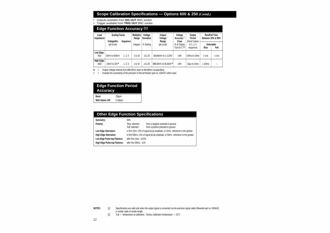
Scope Calibration Specifications — Options 600 & 250 (Contd.)
• Outputs available from SIG OUT BNC socket.• Trigger available from TRIG OUT BNC socket.
Edge Function Accuracy [1]
Load Scaling Factor Multiplier Voltage Output Voltage Output Rise/Fall TimeImpedance Range Deviation Voltage Accuracy ‡ Period Between 10% & 90%
Voltage/Div Sequence Range 1Year (Fixed Values(pk-to-pk) Integers % Setting (pk-to-pk) % of Output in 1, 2, 5 Selectable
Tcal ±5°C [2] sequence) Rise Fall
Low Edge:50Ω 20mV to 500mV 1, 2, 5 1 to 10 ±11.20 88.800mV to 1.1120V ±3% 100ns to 10ms ≤ 1ns ≤ 1ns
High Edge:1MΩ 20mV to 20V ♣ 1, 2, 5 1 to 10 ±11.20 888.00mV to 55.600V ♣ ±3% 10µs to 10ms ≤ 100ns ---
Symmetry: 50%Polarity: 'Rise' selected: from a negative potential to ground.
'Fall' selected: from a positive potential to ground.Low Edge Aberration: in first 10ns: ±2% of signal pk-pk ampliude, or 10mV, whichever is the greater.High Edge Aberration: in first 500ns: ±2% of signal pk-pk ampliude, or 50mV, whichever is the greater.Low Edge Pulse-top Flatness: after first 10ns: ±0.5%High Edge Pulse-top Flatness: after first 500ns: ±1%
♣ = Output Voltage extends from 888.00mV down to 88.800mV (unspecified).‡ = Includes the uncertainty of the precision in-line terminator (part no. 630447) when used.
NOTES: [1] Specifications are valid only when the output signal is connected via the precision signal cable (Wavetek part no. 630442)or similar cable of similar length.
[2] Tcal = temperature at calibration. Factory calibration temperature = 23°C
Basic 25ppmWith Option 100 0.25ppm
Edge Function PeriodAccuracy
Other Edge Function Specifications
23
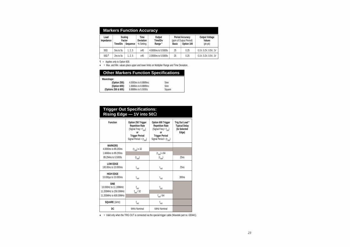
¶ = Applies only to Option 600.♦ = Max. and Min. values place upper and lower limits on Multiplier Range and Time Deviation.
Load Scaling Time Output Period Accuracy Output VoltageImpedance Factor Deviation Time/Div (ppm of Output Period) Values
Time/Div Sequence % Setting Range ♦ Basic Option 100 (pk-pk)
50Ω 5ns to 5s 1, 2, 5 ±45 4.0000ns to 5.5000s 25 0.25 0.1V, 0.2V, 0.5V, 1V
50Ω ¶ 2ns to 5s 1, 2, 5 ±45 2.0000ns to 5.5000s 25 0.25 0.1V, 0.2V, 0.5V, 1V
Markers Function Accuracy
Function Option 250 Trigger Option 600 Trigger Trig Out Lead ♠
Repetition Rate Repetition Rate Typical Delay(Signal Freq = fout) (Signal Freq = fout) (to Selected
or or Edge)Trigger Period Trigger Period
Signal Period = (τout) Signal Period = (τout)
MARKERS4.0000ns to 89.293ns (τout) x 321.6666ns to 89.293ns (τout) x 6489.294ns to 5.5000s (τout) (τout) 25ns
LOW EDGE100.00ns to 10.000ms τout τout 25ns
HIGH EDGE10.000µs to 10.000ms τout τout 300ns
SINE10.000Hz to 11.199MHz fout fout
11.200MHz to 250.00MHz fout / 3211.200MHz to 600.00MHz fout / 64
SQUARE (1kHz) fout fout
DC 64Hz Nominal 64Hz Nominal
♠ = Valid only when the TRIG OUT is connected via the special trigger cable (Wavetek part no. 630441).
Trigger Out Specifications:Rising Edge — 1V into 50Ω
Waveshape:(Option 250): 4.0000ns to 8.8889ns: Sine(Option 600): 1.6666ns to 8.8889ns: Sine
(Options 250 & 600): 8.8888ns to 5.5000s: Square
Other Markers Function Specifications
25
9100 Universal Calibration SystemIncluding Thermocouple Pod, 9105 Lead Kit Assembly andTraceable Calibration CertificateOption PLC Procedure Library Card (each). (See
'Procedure Library' on www.wavetek.com)Option 10 Blank 256k Byte, Programmable (FLASH)
Memory Card. (Use only for procedures)Option 30 Blank 256k Byte, Static (SRAM) Memory Card.
(Use for Results Data)Option 50 Tracker BallOption 60 Soft Carrying CaseOption 90 Rack Mounting KitOption 100 High Stability Crystal Reference.
(Recommended for use with options 250 and600)
Option 200 10 and 50 turn Current CoilsOption 250 250MHz Oscilloscope Calibration Module
(installs internally — includes 4 cables, teeadapter and 50 ohm terminators)
orOption 600 600MHz Oscilloscope Calibration Module
(installs internally — includes 4 cables, teeadapter and 50 ohm terminators)
9010 Windows Automated Calibration Software and ISO 9000Database Manager (including full networking capabilitiesand procedure library). Includes: CD-ROM, user handbook,R & R Report Writer package. Suitable for use with 9x00calibrators.Notes: To control equipment using GPIB interface you will
require Option 20.To generate procedure cards you will require Option40.To run an additional Networked Workstation you willrequire the Network Node
Option 10 Software SupportAn Annual maintenance program whichprovides telephone support, software upgradesand access to new procedures released onwebsite: www.wavetek.com, during themaintenance period (12 months from date ofdelivery). Customer details (i.e. contact name)must be supplied with order.
Option 20 GPIB Interface and Security KeyOption 40 PCMCIA Read/Write module (for desktop
computer only)Option 60 Upgrade to version 1.6Option 70 Hewlett Packard™ Bar Code ReaderNetwork Node Additional Network Node
Ordering Information
26
AustriaWavetek Gesellschaft mbH.Pharos HausNordbahnstrasse 36/TOP 1.4 Tel: (43) 1-214-5110A-1020 Vienna, Austria Fax: (43) 1-214-5109
ChinaWavetek CorporationRoom 2701, Citic BuildingNo. 19 Jianguomenwai Dajie Tel: (86) 10-6592-8044Beijing 100004, China Fax: (86) 10-6500-8199
FranceWavetek S. A.Immeuble le Seine St Germain12, Bd des iles, Bat B 3ème étage,92130 Issy-Les-Moulineaux, Tel: (33) 1-4190-6666France Fax: (33) 1-4190-6650
GermanyWavetek GmbHGutenbergstrasse 2-4 Tel: (49) 89-996-41085737 Ismaning, Germany Fax: (49) 89-996-41160
Hong KongWavetek Hong Kong Ltd.3A HKPC Building78 Tat Chee Avenue Tel: (852) 2788-6221Kowloon, Hong Kong Fax: (852) 2788-6220
JapanYokogawa Electric CorporationKofu General Business Division155 Takamuro-ChoKofu-Shi Tel: 81 552 43 0332Yamanashi-ken, Japan 400 Fax: 81 552 43 0399
SingaporeWavetek Asia-Pacific Pte Ltd51 Goldhill Plaza#14-04/05 Tel: (65) 356-2522Singapore 308900 Fax: (65) 356-2553
United KingdomWavetek LtdHurricane Way Tel: (44) 1603-404824Norwich, Norfolk NR6 6JB, U.K. Fax: (44) 1603-483670
United StatesWavetek Corporation9045 Balboa Avenue Tel: (1) 619-279-2200San Diego, CA 92123, U.S.A. Fax (1) 619-450-0325
Web Sitewww.wavetek.com
Worldwide Sales Offices
Recommended


![Dion[1] 9100](https://img.pdfslide.us/doc/110x75/5549052eb4c90565458b4d76/dion1-9100.jpg)