1
ELE 312Digital Electronics
• DeMassa and Ciccone, Digital Integrated Circuits, John Wiley & Sons.
• Taub and Schilling, Digital Integrated Electronics, McGraw-Hill
Textbooks

2
Contents
• Basic Properties of Digital Integrated Circuits• Diode Digital Circuits• BJT Digital Circuits
– Ebers & Moll equations– Transistor modelling– State of transistor in a circuit
• Resistor-Transistor Logic (RTL)• Diode-Transistor Logic (DTL)• Transistor-Transistor Logic (TTL)• Schottky Transistor – Transistor Logic (STTL)• Different TTL Gates• Emitter-Coupled Logic (ECL)• MOS Digital Circuits• NMOS Gates• CMOS Gates
Properties of Digital Integrated Circuits

3
Most important elements: Inverter and Noninverter
Idealized Inverter and Voltage Transfer Characteristics( VTCs)

4
Propagation Delays
Rise and fall times and turn-on and turn-off times

5
Power dissipation
Logic Element Equivalent Circuit and Fan-out
6
Speed-power product = (Average Power Diss) x (Propagation Delay)
Power - Delay Product:
PD = PDISS(avg) x tP(avg)
Diode Digital Circuits

7
Diodes
)1(eII TD/VVSD −=
Shockleys Eq
VD ≅ V0 = 0.7 V
for Forward Bias

8
IV Characteristics
for MN Schottky diodesfor PN Junction diodes
SPICE model
)1(eII TD/VVSD −=′

9
Basic Logic Gates: AND
Basic Logic Gates: OR

10
Clamping Diodes
Level shifting diodes
Level Shifting Diode AND Gate
Level Shifting Diode OR Gate
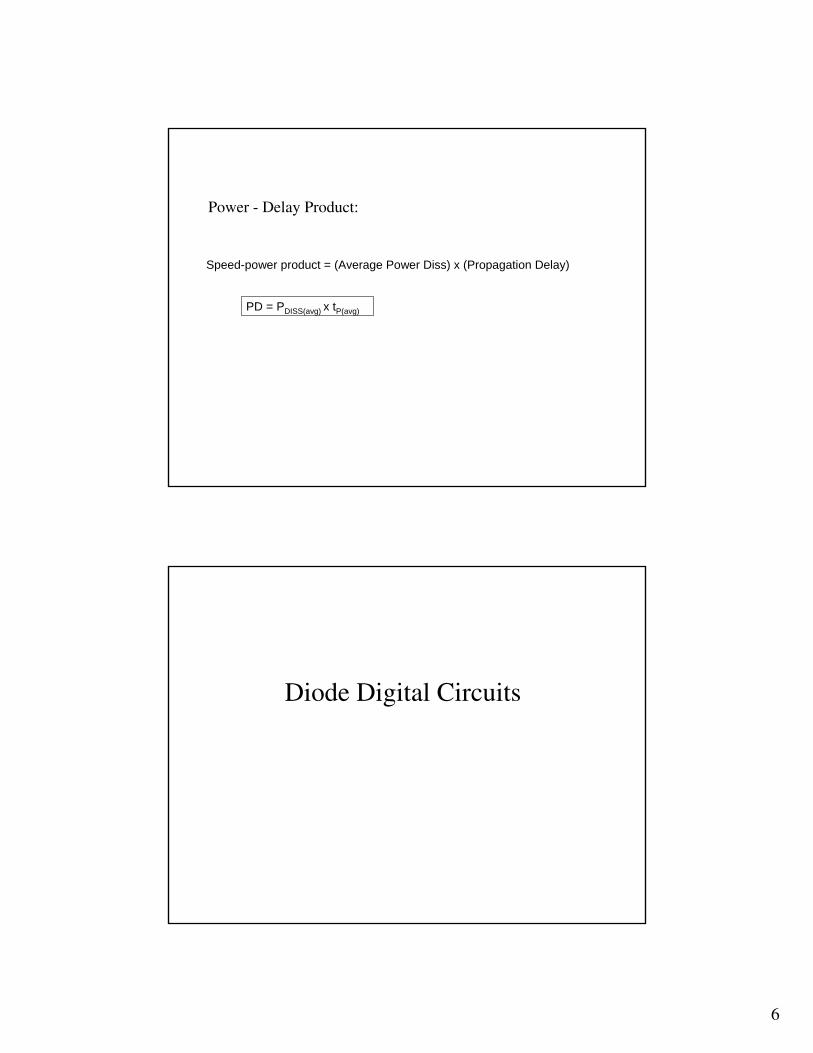
1
BJT Transistors
BJT Fabrication Example

2
Multi-Emitter Fabrication Examples
NPN BJT

3
Ebers-Moll NPN BJT Model
)1e(II TBE V/VESBE,D −=
)1e(II TBC V/VCSBC,D −=
BC,DRBE,DE III α−=
BC,DBE,DFC III −=α
CEB III −=
CSRESF II αα ==SIReciprocity theorem
transport saturation current
Reverse active (RA)ForwardReverse
Saturation (SAT)ForwardForward
Forward active (FA)ReverseForward
Cutoff (OFF)ReverseReverse
ModeBC junctionBE junction
BJT Modes of Operation

4
Reduced models of the operation modes
(a) Cutoff (b) Forward active
(c) Saturation (d) Reverse active
F
FF 1 α
αβ−
=
R
RR 1 α
αβ−
=
1II BFC
≤=
σσβ
IV Characteristics

5
Modes of Operation
Examples
βF = 65IC, IB = ?
Base and emitter voltages = ?

6
TTL Circuit Design
Output-High Pull-up Driver
Output-Low Pull-down Driver
Discharge path and Base-Driving circuitry
7
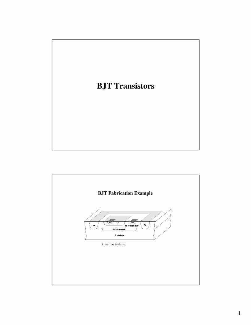
Power Dissipation Example
Resistor-Transistor Logic(RTL)
8
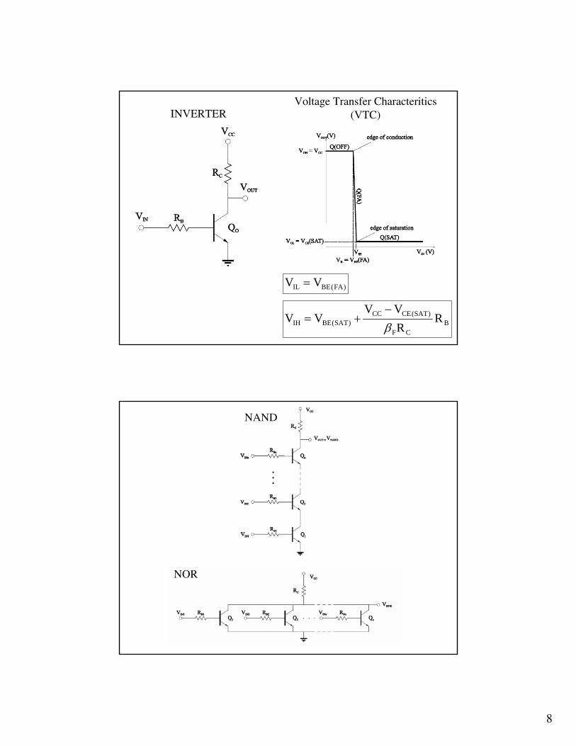
INVERTERVoltage Transfer Characteritics
(VTC)
)FA(BEIL VV =
BCF
)SAT(CECC)SAT(BEIH R
RVV
VVβ−
+=
NOR
NAND

9
RTL Fan-out
RTL fan-out analysis
10
RTL fan-out analysis
Maximum fan-out?
⎥⎦
⎥⎢⎣
⎢=
IN
OUT
IIN
C
OUTCCOUT R
VVI −=
B
)SAT(BEOUTIN R
VVI
−=
IHOUT VV =
BCF
)SAT(CECC)SAT(BEIH R
RVV
VVβ−
+=

11
RTL NONINVERTER

12
AND
OR

1
RTL with Active Pull-up
Fan-out of RTL with Active Pull-up
Determined by the output high state as QS is cut-off for low-inputs
Simplified output high state Simplified input high state

2
Simplified output-high fan-out configuration
⎥⎦
⎥⎢⎣
⎢=
IH
OH
IIN
CP
OUT)SAT(CECCEPOUT R
VVVII
−−≅=
2/RVV
IB
)SAT(BEOUTIN
−=
IH(min)OUT VV =
BCF
)SAT(CECC)SAT(BEIH R
RVV
VVβ−
+=

3
Diode-Transistor Logic(DTL)
Basic DTL Inverter
Basic DTL NAND Gate

4
Diode Modified DTL Inverter
Transistor Modified DTL Inverter

5
VTC of Transistor Modified DTL Inverter
VOH = VCC
VOL = VCE,O(SAT) VIH = VBE,O(SAT) + VBE,L(FA)
VIL = VBE,O(FA) + VBE,L(FA)
DTL Fan-out
Determined by the output low state as DI is off for high-inputs

6
Cascaded DTL
⎥⎦
⎥⎢⎣
⎢=
IL
OL
IIN
RC)SAT(O,COL III −=
C
)SAT(O,CECCRC R
VVI
−= Path 2
)SAT(O,BF)SAT(O,C II σβ=
RDL,EO,B III −=
D
)SAT(O,BERD R
VI =
B
)SAT(O,BE)ON(L,D)FA(L,BECCL,E R
VVVVI
σ−−−
≅
1=σFor maximum fan-outB
)SAT(O,CE)ON(I,DCCIL R
VVVI
−−= Path 3
Example: Calculate the DTL fan-out for βF = 49 and σ = 0.85.
Power Dissipation
Example: Calculate the average power dissipation for the above example?

7
Tansistor-Transistor Logic(TTL)
Basic TTL Inverter
Basic TTL NAND GateBasic DTL Inverter (compare)

8
Actual TTL NAND Gate with Totem Pole Output
VTC of an actual TTL Inverter
VOH = VCC – VBE,P(FA) – VD,L(ON)
VOL = VCE,O(SAT) VIH = VBE,O(SAT) + VBE,S(SAT) – VCE,I(SAT)
VIL = VBE,S(FA) – VCE,I(SAT))
VIB = VBE,O(FA) + VBE,S(FA) – VCE,I(SAT)VOB = VCC – IRCRC – VBE,P(FA) – VD,L(ON)
D
)FA(O,BERDRC R
VII ==

9
States of diodes and BJTs
EOC: Edge of conduction
TTL Fan-out
Determined by the output low state as QI is cut-off for high-inputs

10
Cascaded TTL
⎥⎦
⎥⎢⎣
⎢=
IL
OL
IIN
)SAT(O,BF)SAT(O,COL III σβ==C
)SAT(O,BE)SAT(S,CECCS,C R
VVVI
−−=
Path 2RD)SAT(S,E)SAT(O,B III −=
D
)SAT(O,BERD R
VI =
B
)SAT(O,BE)SAT(S,BE)RA(I,BCCCI,B R
VVVVI
−−−=
1=σFor maximum fan-out
S,CS,B)SAT(S,E III +=
B
)SAT(O,CE)SAT(I,BECCIL R
VVVI
−−=
Path 1
I,BR)RA(I,CS,B I)1(II β+==
Example: Calculate the TTL fan-out for βF = 25, σ = 0.85 and βR = 0.1
Example (Power Dissipation)
Example: Calculate the average power dissipation for the above example?
PCC(avg) = 10.4 mW
IRB(OL) = 675 μA
IRC(OL) = 2.5 mA
IIL= IRB(OH) = 1 mA
IOL= 51.9 mA51
IIN
IL
OL =⎥⎦
⎥⎢⎣
⎢=
Example (TTL Fan-out)

1
Open-Collector TTL
Mostly used in data busses where multiple gate outputs must be ANDed.
• This can be accomplished by using a single pull-up resistor with open-collector TTL gates• This type of connection is referred to as wired-AND.
Low Power TTL (LTTL)
Accomplished simply by increasing the resistance values. However this results in
• Decreased fan-out• Longer transient-response times

2
LTTL Example
Compare the power dissipation of the LTTL and TTL gates.
IRB(OL) = 67.5 μA
IRC(OL) = 200 μA
IRB(OH) = 100 μA PCC(avg) = 919 μW
TTL vs LTTL power dissipation ratio = 10.4 / 0.919 = 11.3
High Speed TTL (HTTL)
Accomplished simply by decreasing the resistance values. However this results in
• Increased power dissipation

3
Schottky Tansistor-Transistor Logic(STTL)
Schottky Barrier MN diode
Schottky-clamped BJT (Schottky Transistor)

4
Multi-Emitter Fabrication Examples
Modes of Operation for SBJT
1. OFF2. FA3. On Hard4. Reverse Schottky

5
Example (SBJT)
Example: Draw the VTC graph of the SBJT inverter shown below
STTL NAND Gate

6
STTL NAND Gate (VTC)
VOH = VCC – VBE,P(FA) – VBE,P2(FA)
VOL = VCE,O(HARD) VIH = VBE,O(HARD) + VBE,S(HARD) – VCE,I(HARD)
VIL = VBE,O(FA) + VBE,S(FA)– VCE,I(HARD)
STTL NAND Gate (Device states)
Device state table

7
STTL Fan-out
Determined by the output low state as QI is cut-off for high-inputs
Cascaded STTL
⎥⎦
⎥⎢⎣
⎢=
IL
OL
IIN
)HARD(O,BF)HARD(O,COL III β==C
)HARD(O,BE)HARD(S,CECCS,C R
VVVI
−−=
Path 2, 3)HARD(D,C)HARD(S,E)HARD(O,B III −=
CD
)HARD(D,CE)HARD(O,BE)HARD(D,C R
VVI
−=
B
)HARD(O,BE)HARD(S,BE)RS(I,BCCCSBD R
VVVVI
−−−=
S,CS,B)HARD(S,E III +=
B
)HARD(O,CE)HARD(I,BECCIL R
VVVI
−−=
Path 1
SBD)RS(I,CS,B III ==

8
Example: Calculate the STTL maximum fan-out for βF = 49.
Example (Power Dissipation)
Example: Calculate the average power dissipation for the above example?
PCC(avg) = 20.05 mW
IRB(OL) = 1.11 mA
IRC(OL) = 4.11 mAIIL= IRB(OH) = 1.32 mA
IOL= 197 mA
149IIN
IL
OL =⎥⎦
⎥⎢⎣
⎢=
Example (TTL Fan-out)
IRCD(OL) = 1.20 mA
IR,O(OL) = 4.02 mA
IE,S(OL) = 4.22 mA
IE,P(OL) = 0.182 mA
IE,P(OH) = 1.3 mA
Low Power STTL (LSTTL)
Accomplished by 1. Increasing the resistance value2. Diode input section3. Pull-down enhancements
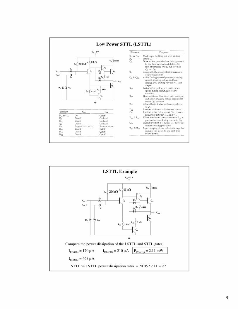
9
Low Power STTL (LSTTL)
LSTTL Example
Compare the power dissipation of the LSTTL and STTL gates.
IRB(OL) = 170 μA
IRC(OL) = 463 μA
IRB(OH) = 210 μA PCC(avg) = 2.11 mW
STTL vs LSTTL power dissipation ratio = 20.05 / 2.11 = 9.5

10
Advanced Schottky Tansistor-Transistor Logic
(ASTTL)
Advanced Schottky Transistor Logic
• Advanced Low-Power Schottky TTL (ALSTTL)
• Fairchild Advanced Schottky TTL (FAST)
• Advanced Schottky TTL (ASTTL)

11
ALSTTL
ALSTTL VTC
VOH = VCC – VBE,P(FA)
VOL = VCE,O(HARD)
VIH = VBE,O(HARD) + VBE,S(HARD) + VBE,SB(HARD) – VBE,IPA(FA)
VIL = VBE,O(FA) + VEB,IPA(FA)

12
ALSTTL VTC
FAST

13
FAST VTC
VOH = VCC – VBE,P(FA)
VOL = VCE,O(HARD)
VIH = VBE,O(HARD) + VBE,S(HARD) + VBE,SB(HARD) – VD,IA(ON)
VIL = VBE,O(FA) + VBE,S(FA) + VBE,SB(FA) – VD,IA(ON)
ASTTL

14
ASTTL

1
Other TTL Gates
Other TTL Gates
• AND gates• NOR gates• OR gates• AND-OR-INVERT (AOI) gates• XOR gates• Schmitt Trigger Inverters and NAND gates• Tri-State buffers

2
TTL AND gate
TTL AND gate - VTC

3
TTL NOR gate
Power Dissipation Example
ICC(LL) = 2 mA
ICC(HL) = 4.175 mA
ICC(LH) = 4.175 mA
PCC(avg) = 17.75 mWICC(HH) = 3.85 mA
IRB(IL) = 1 mA IRB(IH) = 675 μA IRC(OL) = 2.5 mA
TTL NAND gate
TTL OR gate
TTL AND gate
Example: Noise margins VNMH , VNML?
4
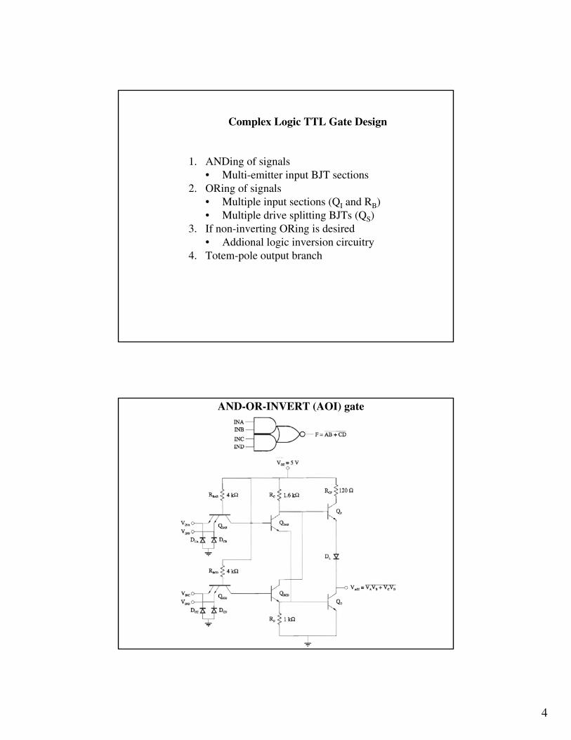
Complex Logic TTL Gate Design
1. ANDing of signals • Multi-emitter input BJT sections
2. ORing of signals • Multiple input sections (QI and RB)• Multiple drive splitting BJTs (QS)
3. If non-inverting ORing is desired• Addional logic inversion circuitry
4. Totem-pole output branch
AND-OR-INVERT (AOI) gate

5
Example
Design a complex logic TTL gate that VOUT = VAVB + VC + VDVEVF
Example
Design a complex logic TTL gate that VOUT = VAVB + VC + VDVEVF

6
TTL XOR gate
Hysteresis and Schmitt Trigger Gates

7
Hysteresis
Base-Emitter coupled Schmitt Trigger Non-inverting circuit
Hysteresis
CCOHS VV =
)SAT(CEeq2CS
)SAT(CECC
1CS
)SAT(BECCOLS VR
RVV
RVV
V +⎟⎟⎠
⎞⎜⎜⎝
⎛ −−
−=
E2CS1CSeq R||R||RR =
)FA(1S,BEeq2CS
)SAT(CECC
1CS
)SAT(BECCIUS VR
RVV
RVV
V +⎟⎟⎠
⎞⎜⎜⎝
⎛ −−
−=
αVVαV
V )FA(2S,BE)SAT(1S,BECCIDS
−+=
1RRα
E
1CS +=

8
Example
Find the VOHS, VOLS, VIUS and VIDS points where RCS1 = 4kΩ, RCS2 = 2.5kΩ, and RES = 1kΩ.
VOHS = 5VVOLS = 2V VIUS = 2.5V
VIDS = 1.66V
Req = 606Ω
ICS1 = 1.05mA
ICS1 = 1.92mA
TTL Schmitt Trigger NAND gate
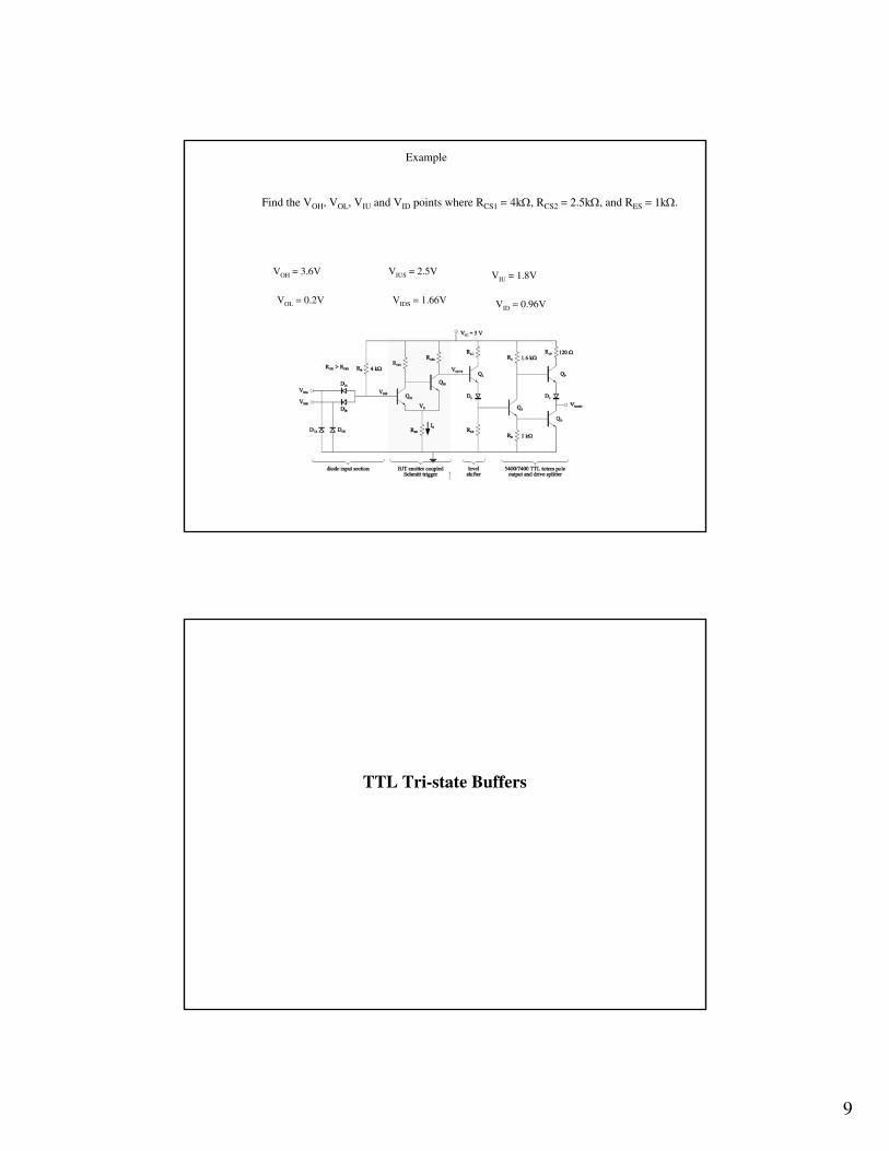
9
Example
Find the VOH, VOL, VIU and VID points where RCS1 = 4kΩ, RCS2 = 2.5kΩ, and RES = 1kΩ.
VOH = 3.6V
VOL = 0.2V
VIUS = 2.5V
VIDS = 1.66V
VIU = 1.8V
VID = 0.96V
TTL Tri-state Buffers

10
TTL Tri-state Buffers
Connecting TTL Tri-state buffers to a Bus

11

1
Emitter-Coupled Logic(ECL)
Basic ECL Inverter/Non-inverter(ECL Current Switch)

2
Basic ECL Inverter/Non-inverter VTC
VOH = VCC
According to inverting output: VINV
CIE
EE)ECL(BEIHCCOL R
RVVV
VV+−
−=
VIL = VBB – 0.05 VIH = VBB + 0.05
E
CI
EE)SAT(BEE
CI)SAT(BCCC
S
RR1
)VV(RRVV
V+
−++=
Example
Calculate the critical VTC points for the ECL current switch
VCC = 5V, VEE = 0V, VBB = 2.6V, RCI = RCR = RE = 1kΩ,
VBE(ECL) = 0.75V, VBE(SAT) = 0.8V, VBC(SAT) = 0.6V
VOH = 5V
VOL = 3.10V
VIL = 2.55V
VIH = 2.65V
VS = 3.2V
VINV (VIN = VS) = 2.6V

3
Basic ECL NOR/OR Gate
4
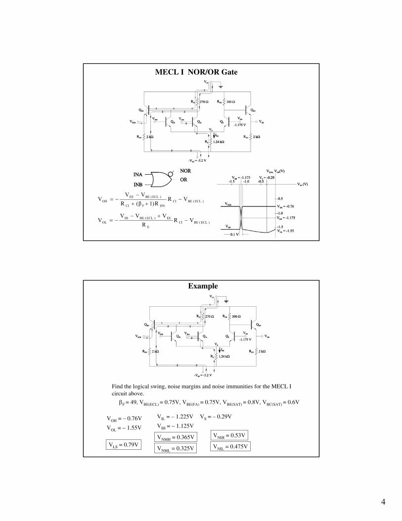
MECL I NOR/OR Gate
)ECL(BECIDNFCI
)ECL(BEEEOH VR
R)1(βRVV
V −++
−−=
)ECL(BECIE
EE)ECL(BEIHOL VR
RVVV
V −+−
−=
Example
Find the logical swing, noise margins and noise immunities for the MECL I circuit above.
βF = 49, VBE(ECL) = 0.75V, VBE(FA) = 0.75V, VBE(SAT) = 0.8V, VBC(SAT) = 0.6V
VOH = – 0.76V
VOL = – 1.55V
VIL = – 1.225V
VIH = – 1.125V
VS = – 0.29V
VLS = 0.79VVNMH = 0.365V
VNML = 0.325V
VNIH = 0.53V
VNIL = 0.475V
5
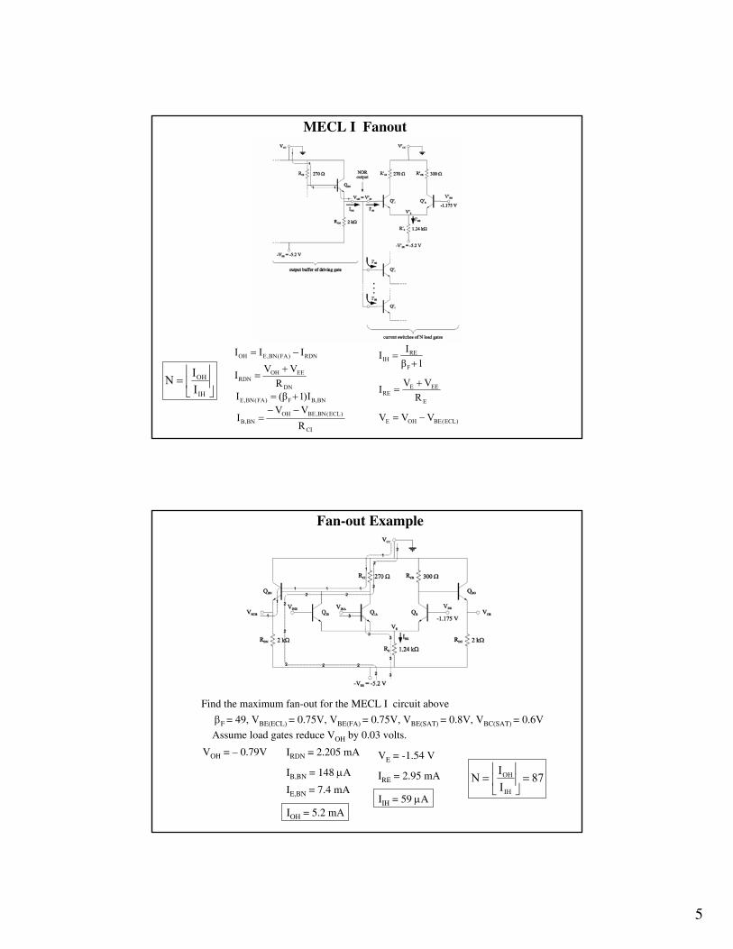
MECL I Fanout
⎥⎦
⎥⎢⎣
⎢=
IH
OH
IIN
RDN)FA(BN,EOH III −=
DN
EEOHRDN R
VVI +=
BN,BF)FA(BN,E I)1(βI +=
CI
)ECL(BN,BEOHBN,B R
VVI
−−=
1βIIF
REIH +=
E
EEERE R
VVI +=
)ECL(BEOHE VVV −=
Fan-out Example
Find the maximum fan-out for the MECL I circuit above
βF = 49, VBE(ECL) = 0.75V, VBE(FA) = 0.75V, VBE(SAT) = 0.8V, VBC(SAT) = 0.6V
Assume load gates reduce VOH by 0.03 volts.
VOH = – 0.79V IRDN = 2.205 mA
IB,BN = 148 μA
IE,BN = 7.4 mA
IOH = 5.2 mA
VE = -1.54 V
IRE = 2.95 mA
IIH = 59 μA
87IINIH
OH =⎥⎦
⎥⎢⎣
⎢=

6
Power Dissipation Example
Find the average power dissipated in the MECL I circuit above
IRE(NOH) = 2.64 mA
IRDN(NOH) = 2.22 mA
IEE(NOH) = 6.685 mA
IRDO(NOH) = 1.825 mA
IRE(NOL) = 2.98 mA
IRDN(NOL) = 1.825 mA
IEE(NOL) = 7.035 mA
IRDO(NOL) = 2.22 mA
PEE(avg) = 35.6 mW
Other ECL Gates
7
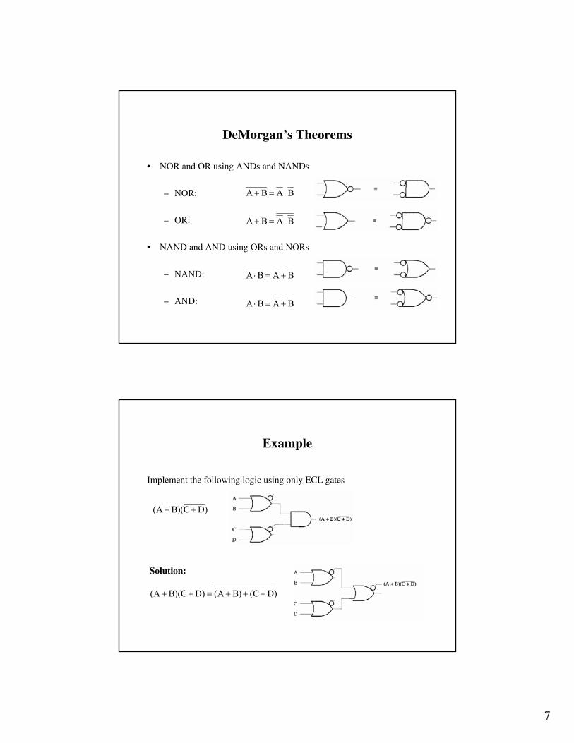
DeMorgan’s Theorems
• NOR and OR using ANDs and NANDs
– NOR:
– OR:
• NAND and AND using ORs and NORs
– NAND:
– AND:
BABA ⋅=+
BABA ⋅=+
BABA +=⋅
BABA +=⋅
Example
Implement the following logic using only ECL gates
)DC)(BA( ++
Solution:
)DC()BA()DC)(BA( +++≡++

8
Collector Dotting Wired-AND Gates
Complex Logic Gates with Collector Dotting

9
Example
Series Gating – Basic ECL NAND/AND Current Switch

10
Series Gating NAND/AND Gate
Complex Logic Gates with Series Gating

11
Example
ECL XOR/XNOR Gates

12
ECL Decoding Tree

1
MOS Logic
MOS Logic
• NMOS gates– Fabrication– Modes of operation
• NMOS Inverters and Analysis– General NMOS Inverter– Resistor Loaded NMOS Inverter– E-MOSFET loaded NMOS Inverter– D-MOSFET loaded NMOS Inverter

2
NMOS (n-channel E-MOSFET) Fabrication Examples
CMOS Fabrication Example

3
IV Characteristics
NMOS modes of operation
(a) Cutoff mode (b) Linear mode
(c) Saturation mode (d) body-bias effect on threshold voltage
4
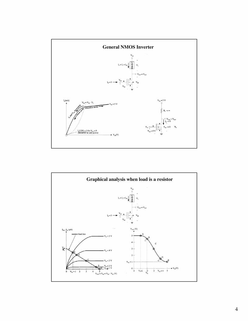
General NMOS Inverter
Graphical analysis when load is a resistor

5
Load capacitance
Power dissipation
PDD = VDD (IDD(OH) + IDD(OL)) / 2
≅ VDD IDD(OL) / 2
(a) Static power dissipation
(b) Transient power dissipation
PD = CL ƒV2DD
ƒ: frequency at which the gate is switched
PTOTAL = PDD + PD

6
Resistor Loaded NMOS
Resistor Loaded NMOS Inverter

7
Propagation Delay
Fall time

8
E-MOSFET Loaded NMOS
E-MOSFET Loaded NMOS Inverter

9
D-MOSFET Loaded NMOS
D-MOSFET Loaded NMOS Inverter

10
NMOS Gates
Symbol Shorthands

11
NOR Gate
NOR Gates

12
NAND Gate
⎟⎟⎠
⎞⎜⎜⎝
⎛+
=BA
OO LL
Wk
)Inverter(V)NAND(V OLOL >
OR Gates
13
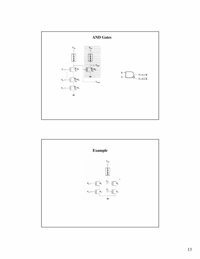
AND Gates
Example

14
AOI (AND-OR-INVERT) Gates
Examples

15
XOR/XNOR Gates
Hysteresis

16
Schmitt Trigger
Transmission Gate

17
Transmission Gate Array
CMOS Logic

18
CMOS Inverter
CMOS Inverter

19
Symmetric CMOS Inverter
Capacitance Effect on Transition - 1

20
Capacitance Effect on Transition - 2
Electrostatic Discharge (ESD) Protection

21
CMOS Gates
Symbol Shorthands

22
CMOS NAND Gate
CMOS NAND Gates

23
CMOS NOR Gate
CMOS NOR Gates

24
CMOS AND/NAND Gate
CMOS OR/NOR Gate

25
CMOS AOI Gates
CMOS AOI Gates

26
CMOS AND-OR Gate
CMOS OAI Gates

27
CMOS AOI Gates
Example

28
Example

29
XOR Gate
Recommended