1Copyright © by Jose E. Schutt-Aine , All Rights ReservedECE 497-JS, Spring 2004
ECE 497 JS Lecture - 18Impact of Scaling
Spring 2004
Jose E. Schutt-AineElectrical & Computer Engineering
University of [email protected]
2Copyright © by Jose E. Schutt-Aine , All Rights ReservedECE 497-JS, Spring 2004
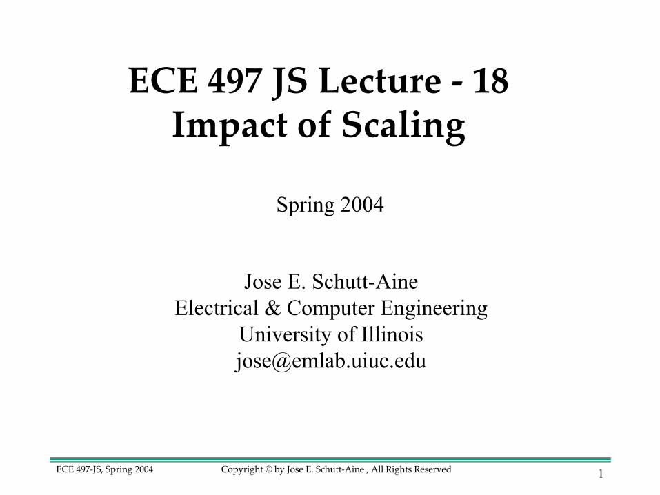
Thursday April 8th Speaker:
Prof. Umberto Ravaioli
Announcements
- NTRA document updated
- Problems using jsa4?
3Copyright © by Jose E. Schutt-Aine , All Rights ReservedECE 497-JS, Spring 2004
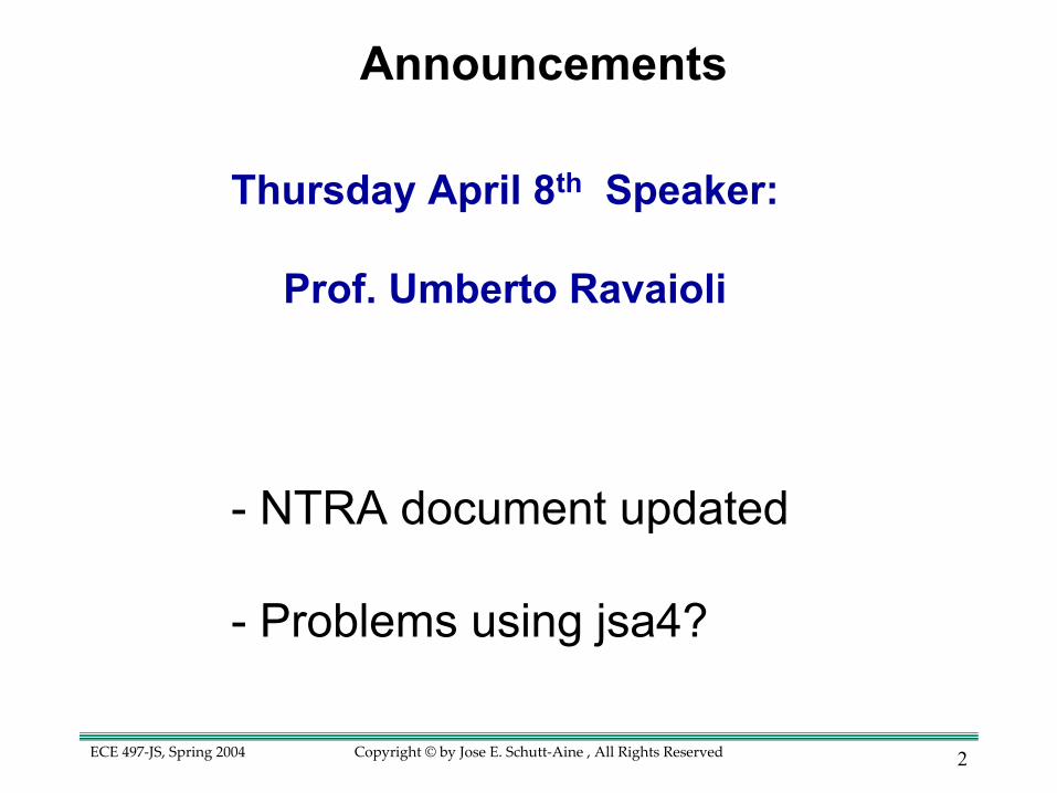
On-Chip IR Drop
• Large Voltage Drop– Example: VIR=0.78V local supply down by 1.56V:unacceptable– Voltage drop across global buses is dependent only on the fraction of
metal layer devoted to each bus
• Remedy– Use area bonded chip so that power need not be distributed from chip
edge– Use more or thicker metal layers– Use on-chip bypass capacitors
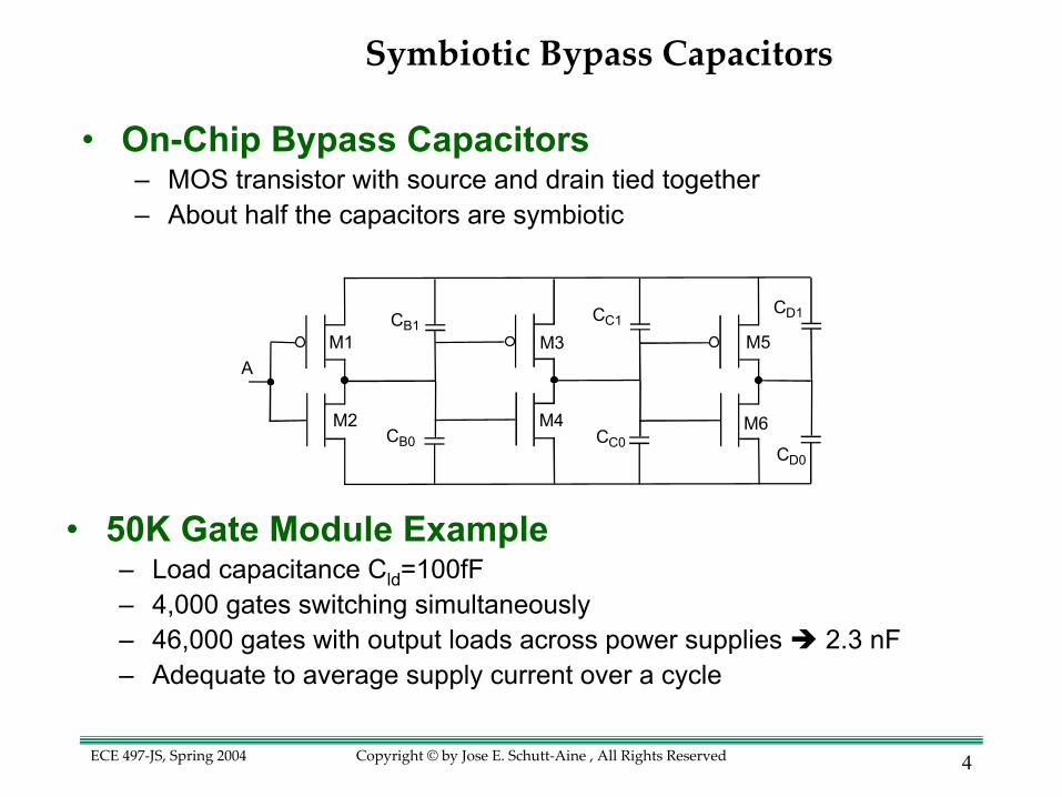
4Copyright © by Jose E. Schutt-Aine , All Rights ReservedECE 497-JS, Spring 2004
M1
M2
M3
M4
M5
M6
CB1
CB0
CC1
CC0
CD1
CD0
A
Symbiotic Bypass Capacitors
• 50K Gate Module Example– Load capacitance Cld=100fF– 4,000 gates switching simultaneously– 46,000 gates with output loads across power supplies 2.3 nF– Adequate to average supply current over a cycle
• On-Chip Bypass Capacitors– MOS transistor with source and drain tied together– About half the capacitors are symbiotic
5Copyright © by Jose E. Schutt-Aine , All Rights ReservedECE 497-JS, Spring 2004
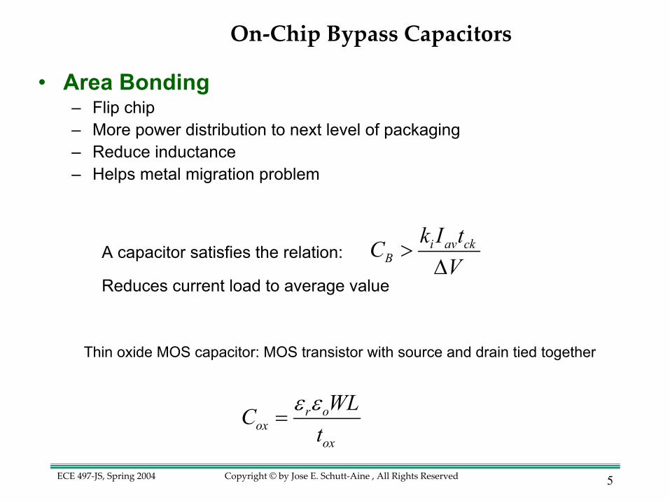
• Area Bonding– Flip chip– More power distribution to next level of packaging– Reduce inductance– Helps metal migration problem
A capacitor satisfies the relation: i av ckB
k I tCV
>∆
Reduces current load to average value
r oox
ox
WLCt
ε ε=
Thin oxide MOS capacitor: MOS transistor with source and drain tied together
On-Chip Bypass Capacitors
6Copyright © by Jose E. Schutt-Aine , All Rights ReservedECE 497-JS, Spring 2004
time time
curr
ent
curr
ent
Before Today
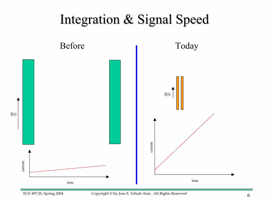
Integration & Signal SpeedIntegration & Signal Speed
I(t)
I(t)
7Copyright © by Jose E. Schutt-Aine , All Rights ReservedECE 497-JS, Spring 2004
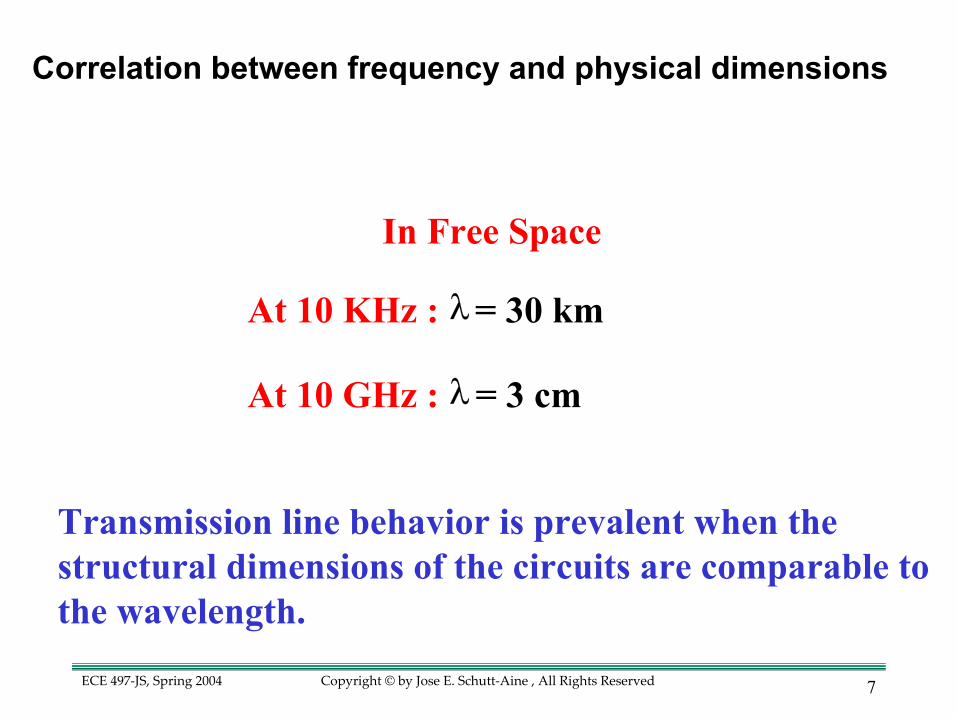
Correlation between frequency and physical dimensions
In Free Space
At 10 KHz : λ= 30 km
At 10 GHz : λ = 3 cm
Transmission line behavior is prevalent when the structural dimensions of the circuits are comparable to the wavelength.
8Copyright © by Jose E. Schutt-Aine , All Rights ReservedECE 497-JS, Spring 2004
Chip size(mm2)
Number of transistors(million)
Interconnect width(nm)
Total interconnect length(km)
1997 2003 20122006
300 430 750520
11 76 200 1400
200 100 70 35
2.16 2.84 5.14 24
Semiconductor Technology TrendsSemiconductor Technology Trends
9Copyright © by Jose E. Schutt-Aine , All Rights ReservedECE 497-JS, Spring 2004
0
5
10
15
20
25
Del
ay (p
s)
30
35
40
45
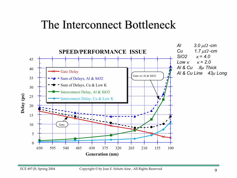
650 595 540 485Generation (nm)
SPEED/PERFORMANCE ISSUE
Gate Delay
Sum of Delays, Al & SiO2
Sum of Delays, Cu & Low K
Interconnect Delay, Al & SiO2
Interconnect Delay, Cu & Low K
430 375 320 265 210 155 100
Gate wi Al & SiO2
Gate
Al 3.0 µΩ -cmCu 1.7 µΩ -cmSiO2 κ = 4.0Low κ κ = 2.0Al & Cu .8µ ThickAl & Cu Line 43µ Long
The Interconnect BottleneckThe Interconnect Bottleneck
10Copyright © by Jose E. Schutt-Aine , All Rights ReservedECE 497-JS, Spring 2004
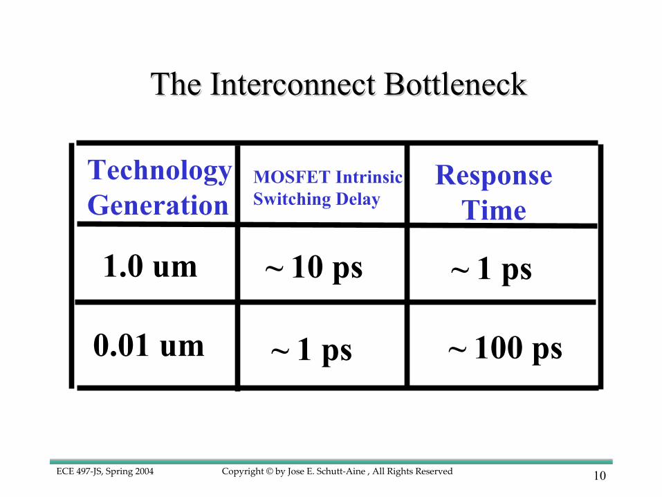
The Interconnect BottleneckThe Interconnect Bottleneck
TechnologyGeneration
MOSFET IntrinsicSwitching Delay
ResponseTime
1.0 um
0.01 um
~ 10 ps
~ 1 ps
~ 1 ps
~ 100 ps
11Copyright © by Jose E. Schutt-Aine , All Rights ReservedECE 497-JS, Spring 2004
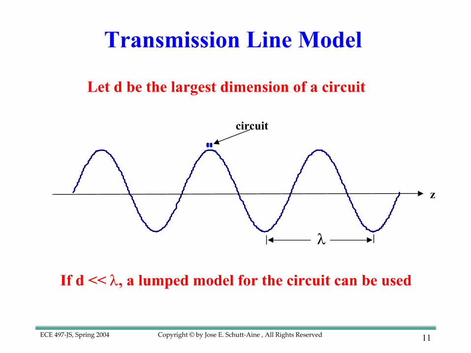
Let d be the largest dimension of a circuit
If d << λ, a lumped model for the circuit can be used
Transmission Line Model
circuit
z
λ
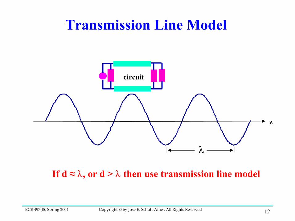
12Copyright © by Jose E. Schutt-Aine , All Rights ReservedECE 497-JS, Spring 2004
Transmission Line Model
circuit
z
λ
If d ≈ λ, or d > λ then use transmission line model
13Copyright © by Jose E. Schutt-Aine , All Rights ReservedECE 497-JS, Spring 2004
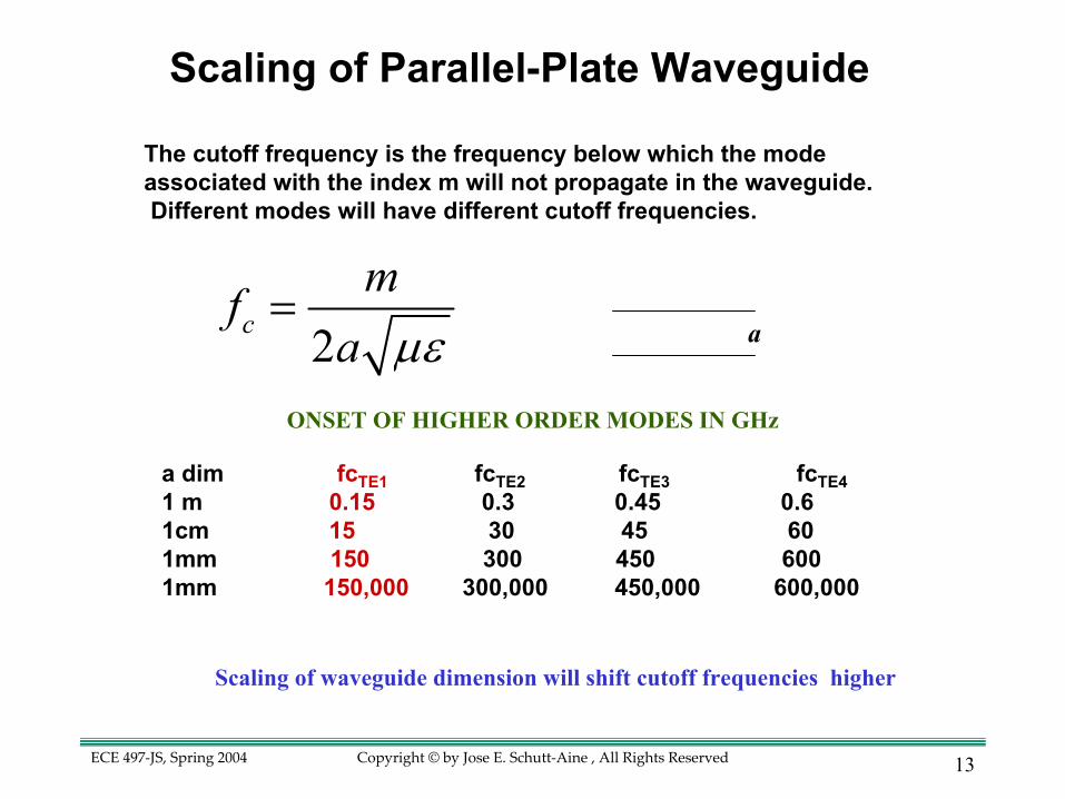
The cutoff frequency is the frequency below which the mode associated with the index m will not propagate in the waveguide. Different modes will have different cutoff frequencies.
2cmf
a µε=
a dim fcTE1 fcTE2 fcTE3 fcTE41 m 0.15 0.3 0.45 0.6 1cm 15 30 45 601mm 150 300 450 6001mm 150,000 300,000 450,000 600,000
ONSET OF HIGHER ORDER MODES IN GHz
a
Scaling of Parallel-Plate Waveguide
Scaling of waveguide dimension will shift cutoff frequencies higher
14Copyright © by Jose E. Schutt-Aine , All Rights ReservedECE 497-JS, Spring 2004
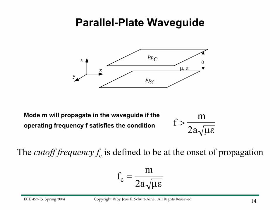
x
zy
PEC
PEC
µ, ε
f >m
2a µε
The cutoff frequency fc is defined to be at the onset of propagation
fc =m
2a µε
a
Parallel-Plate Waveguide
Mode m will propagate in the waveguide if the operating frequency f satisfies the condition
15Copyright © by Jose E. Schutt-Aine , All Rights ReservedECE 497-JS, Spring 2004
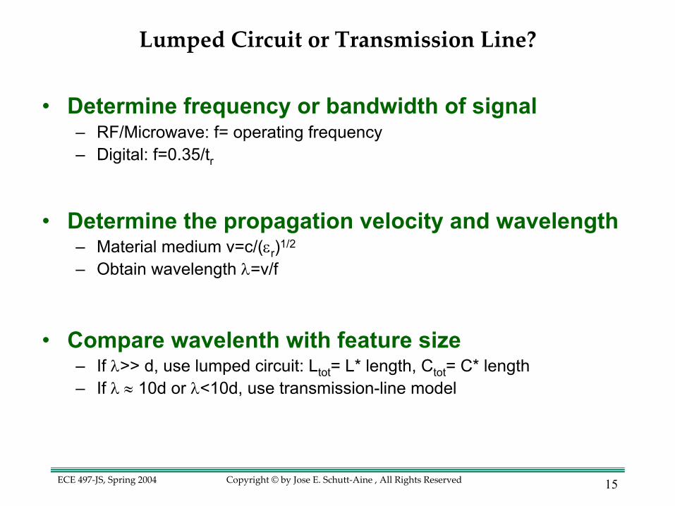
Lumped Circuit or Transmission Line?
• Determine frequency or bandwidth of signal– RF/Microwave: f= operating frequency– Digital: f=0.35/tr
• Determine the propagation velocity and wavelength– Material medium v=c/(εr)1/2
– Obtain wavelength λ=v/f
• Compare wavelenth with feature size – If λ>> d, use lumped circuit: Ltot= L* length, Ctot= C* length– If λ ≈ 10d or λ<10d, use transmission-line model
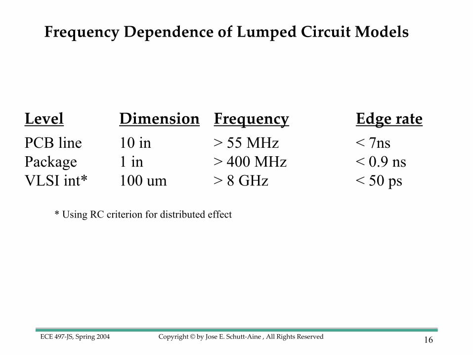
16Copyright © by Jose E. Schutt-Aine , All Rights ReservedECE 497-JS, Spring 2004
PCB line 10 in > 55 MHz < 7nsPackage 1 in > 400 MHz < 0.9 nsVLSI int* 100 um > 8 GHz < 50 ps
Level Dimension Frequency Edge rate
* Using RC criterion for distributed effect
Frequency Dependence of Lumped Circuit Models
17Copyright © by Jose E. Schutt-Aine , All Rights ReservedECE 497-JS, Spring 2004
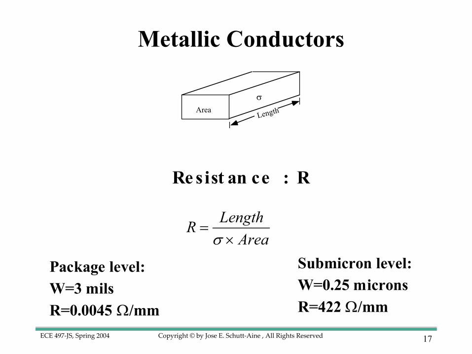
Metallic Conductors
Length
σArea
Re sist an ce : R
Package level:W=3 milsR=0.0045 Ω/mm
Submicron level:W=0.25 micronsR=422 Ω/mm
LengthRAreaσ
=×
18Copyright © by Jose E. Schutt-Aine , All Rights ReservedECE 497-JS, Spring 2004
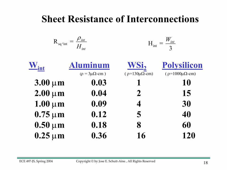
3.00 µm 0.03 1 102.00 µm 0.04 2 151.00 µm 0.09 4 300.75 µm 0.12 5 400.50 µm 0.18 8 600.25 µm 0.36 16 120
Wint Aluminum WSi2 Polysilicon(ρ = 3µΩ-cm ) ( ρ=130µΩ-cm) ( ρ=1000µΩ-cm)
sq intR . = int
intHρ
intH = 3intW
Sheet Resistance of Interconnections
19Copyright © by Jose E. Schutt-Aine , All Rights ReservedECE 497-JS, Spring 2004
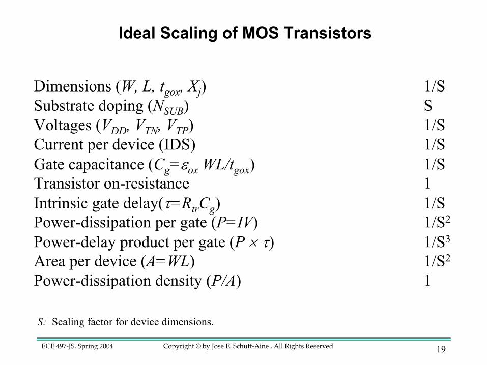
Dimensions (W, L, tgox, Xj) 1/SSubstrate doping (NSUB) SVoltages (VDD, VTN, VTP) 1/SCurrent per device (IDS) 1/SGate capacitance (Cg=εox WL/tgox) 1/STransistor on-resistance 1Intrinsic gate delay(τ=RtrCg) 1/SPower-dissipation per gate (P=IV) 1/S2
Power-delay product per gate (P × τ) 1/S3
Area per device (A=WL) 1/S2
Power-dissipation density (P/A) 1
Ideal Scaling of MOS Transistors
S: Scaling factor for device dimensions.
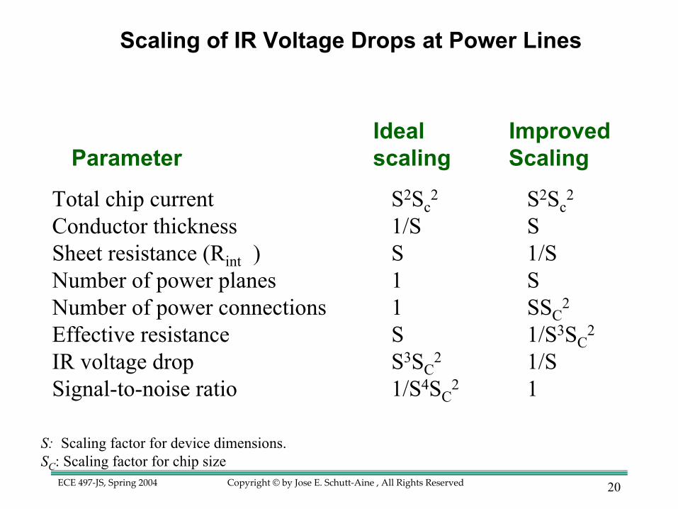
20Copyright © by Jose E. Schutt-Aine , All Rights ReservedECE 497-JS, Spring 2004
Total chip current S2Sc2 S2Sc
2
Conductor thickness 1/S SSheet resistance (Rint) S 1/SNumber of power planes 1 SNumber of power connections 1 SSC
2
Effective resistance S 1/S3SC2
IR voltage drop S3SC2 1/S
Signal-to-noise ratio 1/S4SC2 1
Ideal ImprovedParameter scaling Scaling
Scaling of IR Voltage Drops at Power Lines
S: Scaling factor for device dimensions.SC: Scaling factor for chip size
21Copyright © by Jose E. Schutt-Aine , All Rights ReservedECE 497-JS, Spring 2004
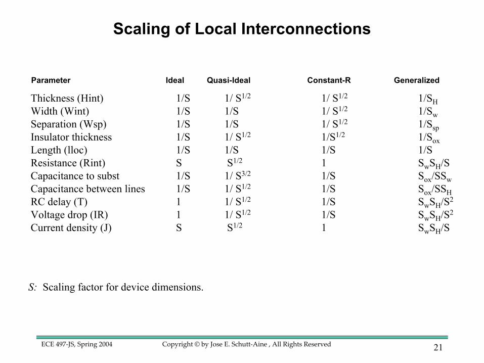
Thickness (Hint) 1/S 1/ S1/2 1/ S1/2 1/SHWidth (Wint) 1/S 1/S 1/ S1/2 1/SwSeparation (Wsp) 1/S 1/S 1/ S1/2 1/SspInsulator thickness 1/S 1/ S1/2 1/S1/2 1/SoxLength (lloc) 1/S 1/S 1/S 1/SResistance (Rint) S S1/2 1 SwSH/SCapacitance to subst 1/S 1/ S3/2 1/S Sox/SSwCapacitance between lines 1/S 1/ S1/2 1/S Sox/SSHRC delay (T) 1 1/ S1/2 1/S SwSH/S2
Voltage drop (IR) 1 1/ S1/2 1/S SwSH/S2
Current density (J) S S1/2 1 SwSH/S
Scaling of Local Interconnections
Parameter Ideal Quasi-Ideal Constant-R Generalized
S: Scaling factor for device dimensions.
22Copyright © by Jose E. Schutt-Aine , All Rights ReservedECE 497-JS, Spring 2004
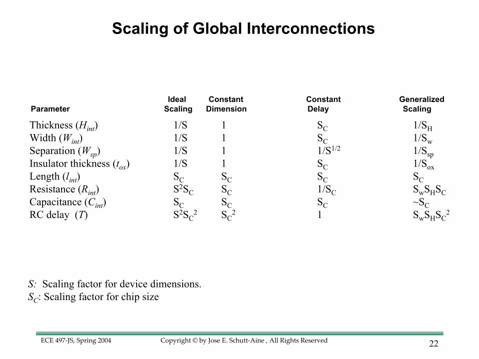
Thickness (Hint) 1/S 1 SC 1/SHWidth (Wint) 1/S 1 SC 1/SwSeparation (Wsp) 1/S 1 1/S1/2 1/SspInsulator thickness (tox) 1/S 1 SC 1/SoxLength (lint) SC SC SC SCResistance (Rint) S2SC SC 1/SC SwSHSCCapacitance (Cint) SC SC SC ~SCRC delay (T) S2SC
2 SC2 1 SwSHSC
2
Ideal Constant Constant Generalized Parameter Scaling Dimension Delay Scaling
Scaling of Global Interconnections
S: Scaling factor for device dimensions.SC: Scaling factor for chip size
23Copyright © by Jose E. Schutt-Aine , All Rights ReservedECE 497-JS, Spring 2004
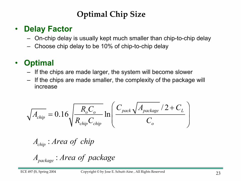
Optimal Chip Size
• Delay Factor– On-chip delay is usually kept much smaller than chip-to-chip delay– Choose chip delay to be 10% of chip-to-chip delay
• Optimal– If the chips are made larger, the system will become slower– If the chips are made smaller, the complexity of the package will
increase
/ 20.16 ln pack package Lo o
chipchip chip o
C A CR CAR C C
+ =
: chipA Area of chip
: packageA Area of package
24Copyright © by Jose E. Schutt-Aine , All Rights ReservedECE 497-JS, Spring 2004
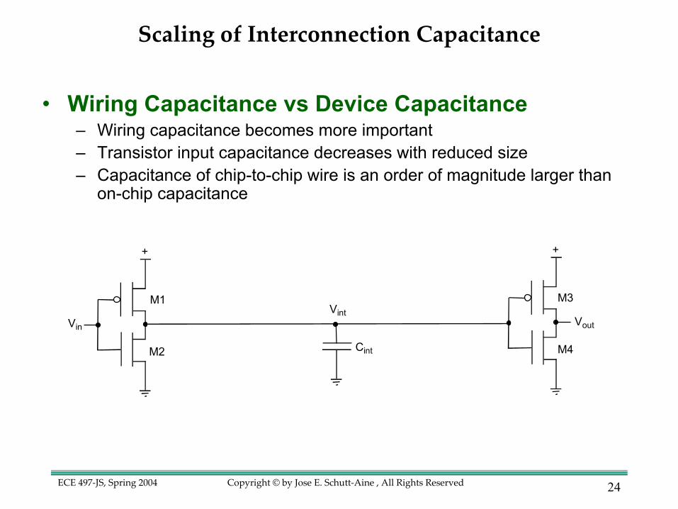
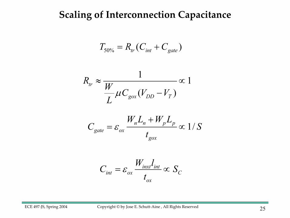
Scaling of Interconnection Capacitance
• Wiring Capacitance vs Device Capacitance– Wiring capacitance becomes more important– Transistor input capacitance decreases with reduced size– Capacitance of chip-to-chip wire is an order of magnitude larger than
on-chip capacitance
+ +
M1
M2
Vin
VintVout
M3
M4Cint
25Copyright © by Jose E. Schutt-Aine , All Rights ReservedECE 497-JS, Spring 2004
50% ( )tr int gateT R C C= +
1 1( )
tr
gox DD T
R W C V VL
µ≈ ∝
−
1/n n p pgate ox
gox
W L W LC S
tε
+= ∝
inxt intint ox C
ox
W lC St
ε= ∝
Scaling of Interconnection Capacitance
26Copyright © by Jose E. Schutt-Aine , All Rights ReservedECE 497-JS, Spring 2004
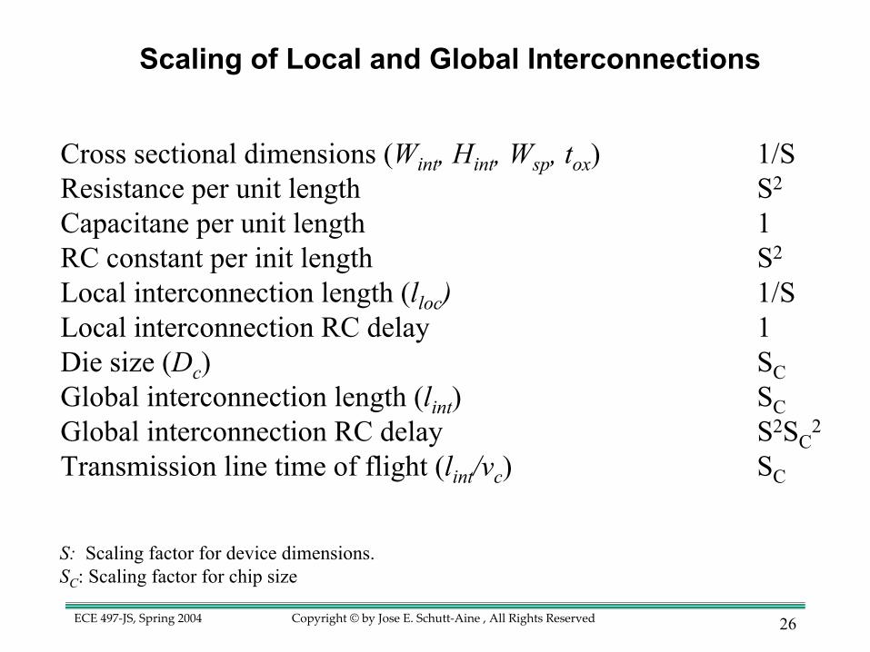
Cross sectional dimensions (Wint, Hint, Wsp, tox) 1/SResistance per unit length S2
Capacitane per unit length 1RC constant per init length S2
Local interconnection length (lloc) 1/SLocal interconnection RC delay 1Die size (Dc) SCGlobal interconnection length (lint) SCGlobal interconnection RC delay S2SC
2
Transmission line time of flight (lint/vc) SC
Scaling of Local and Global Interconnections
S: Scaling factor for device dimensions.SC: Scaling factor for chip size
27Copyright © by Jose E. Schutt-Aine , All Rights ReservedECE 497-JS, Spring 2004
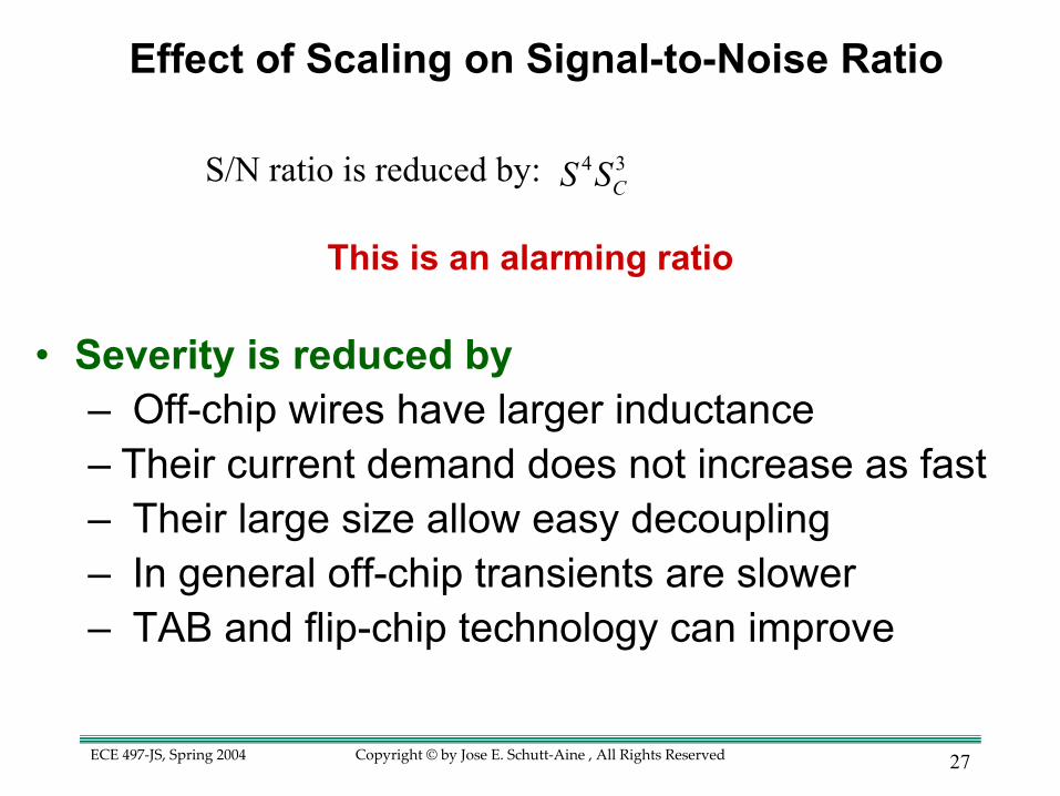
• Severity is reduced by– Off-chip wires have larger inductance– Their current demand does not increase as fast– Their large size allow easy decoupling– In general off-chip transients are slower– TAB and flip-chip technology can improve
Effect of Scaling on Signal-to-Noise Ratio
S/N ratio is reduced by:
This is an alarming ratio
4 3CS S
Recommended


![ECE 598 JS Lecture 02 Resistance, Capacitance, Inductancejsa.ece.illinois.edu/ece598js/Lect_03.pdf · Title: Microsoft PowerPoint - Lect_03 [Compatibility Mode] Author: StoneCreek](https://img.pdfslide.us/doc/110x75/5fa714828dd2e76b7644a833/ece-598-js-lecture-02-resistance-capacitance-title-microsoft-powerpoint-lect03.jpg)
![ECE 598 JS Lecture 06 Multiconductorsjsa.ece.illinois.edu/ece598js/Lect_06.pdf · 2013-03-23 · Title: Microsoft PowerPoint - Lect_06 [Compatibility Mode] Author: jose Created Date:](https://img.pdfslide.us/doc/110x75/5e89ff4b3514a836a87544bf/ece-598-js-lecture-06-2013-03-23-title-microsoft-powerpoint-lect06-compatibility.jpg)