E84 Lab 3: Transistor
Cherie Ho and Siyi Hu
April 18, 2016

Transistor Testing 1. Take screenshots of both the input and output characteristic plots observed on the
semiconductor curve tracer with the following clear labeled (with meaningful increment): ○ The voltage (horizontal axis) or V BE V CE ○ The current (vertical axis) or IB IC ○ For the output plot, each one of the 12 values in the familyIB
Figure 1: Input characteristic plot (Vertical 1mA increment)
Figure 1 shows that when is greater than 1mA..7VV BE ≈ 0 IB
Figure 2: Output characteristic plot

● Determine the value (also referred to as the ``forward transfer current ratio''I /Iβ = C B and denoted by or on the 2N3904 datasheet (also see class notes) from thehf hFE output plot for each of the 5 transistors. From the output characteristic plot, . According to the00β = ΔIB
ΔIC = 1.9 mA−0.9 mA0.01 mA−0.005 mA = 2
datasheet, for . Therefore, the value calculated from Figure 20070 < hf < 3 mAIC ≈ 1 β is consistent with the datasheet value.
● Determine from the input plot when is within the range of 0.01 to 0.1 mA, i.e.,V BE IB
is within the range of to . IC .01β0 .1β0
Figure 3: Input characteristic plot (Vertical 0.1mA increment)
Figure 3 shows that for in the range of 0.01 to 0.1 mA, . This is prettyIB .6VV BE ≈ 0 close to when . We can still approximate as 0.7V when .7VV BE ≈ 0 0.1 mAIB > V BE IB is in the range of 0.01 to 0.1 mA to simplify calculation.
● Describe how the load line changes in the output plot when and are increased orRC V CC decreased.

Figure 4: Load line and output characteristic plot
The light gray plots in Figure 4 are the output characteristic plots. The load lines are
straight lines with slope vertical intersection and horizontal intersection . As Rc− 1RC RC
V CC V CC
increases, the slope of the load line is less negative as shown in the plot on the right. Similarly, as Rc decreases, the slope will be more negative. As Vcc increases, the slope of the load line stays the same, but the load line shifts to the right. That means as Vcc decreases, the load line shifts to the left.
Transistor Circuit Construction 1. Design and build the voltage amplifier based on fixed biasing shown below. Determine
the value of , , and to achieve maximum voltage amplification and minimumRB RC V CC distortion by setting the DC operating point to be in the middle of the linear range of the output characteristic plot. The values of capacitors should be large enough so theC impedance can be assumed to be zero approximately for the signal/jωCZC = 1 frequency .ω

Figure 5: Transistor amplification circuit I
We set . For DC operating point, and can be ignored, since they only2VV CC = 1 V in Rs produce AC voltage. Assume , so ..7VV BE ≈ 0 IB = RB
V −VCC BE = RB11.3V
Since the DC operating point is expected to be in the middle of the linear range of the output characteristic plot, we get , so .I 00IIC = β B = 2 B = RB
2260V RV out = V CC − IC C Given and , we wanted to find and such thatIC = RB
2260V 2V RV out = 1 − IC C RB RC
./2 VV out ≈ V CC = 6 Although we wanted high values to increase the gain, we need to ensure is atRC IB least 0.1 mA so that the approximation still holds. We chose.7VV BE ≈ 0
,20kΩRB = 8 00ΩRC = 2 We used and to achieve maximum gain. The impedance of the0 μCC = 1 80 kHzω = 2 capacitor is , which is negligible compared with the resistor values.Z | .36 Ω| C = 1
ωC = 0
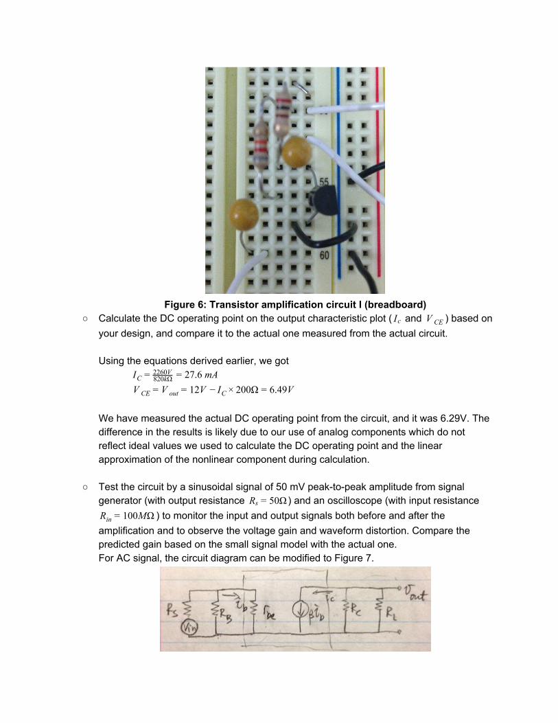
Figure 6: Transistor amplification circuit I (breadboard)
○ Calculate the DC operating point on the output characteristic plot ( and ) based onIc V CE your design, and compare it to the actual one measured from the actual circuit. Using the equations derived earlier, we got
7.6 mAIC = 820kΩ2260V = 2
2V 00Ω .49VV CE = V out = 1 − IC × 2 = 6 We have measured the actual DC operating point from the circuit, and it was 6.29V. The difference in the results is likely due to our use of analog components which do not reflect ideal values we used to calculate the DC operating point and the linear approximation of the nonlinear component during calculation.
○ Test the circuit by a sinusoidal signal of 50 mV peaktopeak amplitude from signal generator (with output resistance ) and an oscilloscope (with input resistance0ΩRs = 5
) to monitor the input and output signals both before and after the00MΩRin = 1 amplification and to observe the voltage gain and waveform distortion. Compare the predicted gain based on the small signal model with the actual one. For AC signal, the circuit diagram can be modified to Figure 7.

Figure 7: AC amplification circuit I On the input side, the input resistance is , since , where||rRin = RB be ≈ rbe rbe ≈ η IB
V T
and , is a few hundred ohms and is in kΩ. ThenIB = RBV −0.7Vcc .026VV T ≈ 0 RB
, so .vbe = vinRin
R +Rin s= vin
rber +Rbe s
ib =vbrbe≈ vinr +Rbe s
The output resistance is , since is in kΩ and Then,||RRout = RC L ≈ RC RC M.RL = 1 . The AC gain is− R − i R −vout = ic out = β b C = β v Rin C
r +Rbe s
−A = vinvout = β RC
r +Rbe S
For the parameters used in this design problem, the expected gain is 168. The negative sign means there is a phase shift of 180°.
Figure 8: Output with Vpp = 50 mV Sinusoidal Input of 280 kHz
Input Vpp Output Vpp Experimental gain Expected gain
50 mV 5.71 V 114 168
The experimental gain measured is lower than expected. This is possibly due to the distortion as the DC operating point is not half of Vcc. It is most likely due to our use of analog components which do not reflect ideal values we used to calculate the DC operating point.
○ Observe the polarity inversion and the signal distortion. Increase the amplitude of the input sinusoid from 50 mV to 1 V and observe the output in terms of the amount of distortion and clipping at both the positive and negative peaks of the sinusoid.

Figure 9: Output with Vpp = 1 V Sinusoidal Input of 280 kHz
(the top cursor is at 0V) From Figures 8 and 9, we see that there is more distortion and clipping for an input sinusoid of a larger amplitude. There is more clipping at 1V as the output amplitude is larger than at 50 mV and is higher than the threshold of the transistor. Distortion is caused if the AC component is too high, which means the transistor is not operating in the linear region. When the input sinusoid is higher, there is more distortion as the input is closer to the saturation or the limit of the transistor circuit.
2. Repeat the above for the amplifier based on a selfbiasing circuit shown in the figure below. Determine the values of , , , and to achieve maximum voltageR1 R2 Rc RE amplification and minimum distortion by setting the DC operating point to be in the middle of the linear range of the output characteristic plot. Hint 1: To minimize distortion, the DC operating point should be around the center of the linear region of the output characteristic plot, i.e., .V CE ≈ V cc/2 Hint 2: write a piece of Matlab code based on the equations for the selfbiasing circuit given here to calculates the DC operating point ( , , , , , andIB Ic V B V c V E V CE = V C − V E
), based on the circuit parameters , , , and that you choose for yourV CC R1 R2 RC RE design.

Figure 10: Transistor amplification circuit II
For the DC operating point, the capacitors are considered as opencircuit. For the source side, using Thevenin’s rule, . Assume ,V , RV Th =
R2R +R1 2 CC Th =
R R1 2R +R1 2
.7VV BE = 0
and IB =V −0.7VTh(β+1)R +RE Th
IC = (β+1)R +RE Th
β(V −0.7V )Th
Again, . We needed to be approximately = 6V2VV CC = 1 (R )V out ≈ V CE − IC C + RE /2V CC while making sure is greater than 0.1 mA. Thus, we choseIB
, .8kΩR1 = 2 0kΩ, R 00Ω, R 40ΩR2 = 2 C = 2 E = 2 The capacitance was kept at .0μF1
Figure 11: Transistor amplification circuit II (breadboard)

○ Calculate the DC operating point on the output characteristic plot ( and ) basedIC V CE on your design, and compare it to the actual one measured from the circuit. Substituting in the designed parameters, we get
2V 0.71VV Th = 200kΩ200kΩ+24kΩ × 1 = 1
.138 mAIB =V −0.7VTh(β+1)R +RE B
= 10.71−0.7V201×240Ω+21.4kΩ = 0
I 00 .138 mA 8.7 mAIC = β B = 2 × 0 = 2 R .13VV C = V out = V CC − IC C = 9
R .45VV E ≈ IC E = 3 .13V .45V .68VV CE = V C − V E = 9 − 3 = 5 .45V .7V .15VV B = V E + V BE = 3 + 0 = 4
The measured DC operating point is around 6.1V. Again the difference might be caused by the uncertainties in the electrical components as well as the linear approximation of the nonlinear semiconductor component. The approximation is less accurate for this circuit than the previous circuit probably because there are more simplifications used in this case for linearizing semiconductor components and eliminating the impedance capacitors.
○ Test the circuit by a sinusoidal signal of 50 mV peaktopeak amplitude from signal generator and an oscilloscope monitor the input and output signals both before and after the amplification and to observe the voltage gain and waveform distortion. Compare the predicted gain based on the small signal model with the actual one.
Figure 12: AC amplification circuit II
The AC amplification of this circuit is similar to the previous circuit. The same derivation and approximation method can be used so that the approximated AC gain is the same.
− − 68A = vinvout = β RC
r +Rbe S= 1
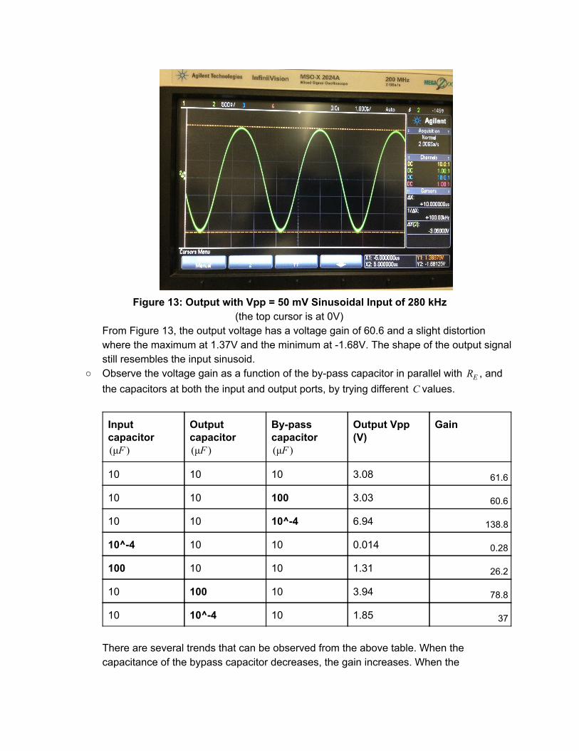
Figure 13: Output with Vpp = 50 mV Sinusoidal Input of 280 kHz
(the top cursor is at 0V) From Figure 13, the output voltage has a voltage gain of 60.6 and a slight distortion where the maximum at 1.37V and the minimum at 1.68V. The shape of the output signal still resembles the input sinusoid.
○ Observe the voltage gain as a function of the bypass capacitor in parallel with , andRE the capacitors at both the input and output ports, by trying different values.C
Input capacitor μF )(
Output capacitor μF )(
Bypass capacitor μF )(
Output Vpp (V)
Gain
10 10 10 3.08 61.6
10 10 100 3.03 60.6
10 10 10^4 6.94 138.8
10^4 10 10 0.014 0.28
100 10 10 1.31 26.2
10 100 10 3.94 78.8
10 10^4 10 1.85 37 There are several trends that can be observed from the above table. When the capacitance of the bypass capacitor decreases, the gain increases. When the

capacitance of the output capacitor increases, the gain also increases. The trend of the input capacitor is interesting. We expect the gain to be larger when the capacitance of the input capacitor increases. However, when the input capacitor is 100, the gain is 26.2 which is much lower than the gain at 10. This may suggest the relationship between the input capacitor and gain is not linear.
○ Observe the voltage gain as a function of the signal frequency. Generate a Bode plot of the magnitude of the voltage gain for the frequency range of 10 Hz to 1 MHz. Find the maximum voltage gain and the frequency range in which this maximum gain isAmax achieved.
Frequency Output Vpp (V) Gain
280 kHz (maximum Amax) 3.08 61.6
10Hz 0.10 2
100 Hz 0.10 2
1 kHz 0.70 14
10 kHz 2.63 52.6
100 kHz 2.93 58.6
1000 kHz 2.83 56.6

Figure 14: Bode Plot of Amplification Circuit Gain vs. Frequency
The bode plot above shows that the frequency range at which there is maximum gain is between 100kHz to 600kHz. From the bode plot, we can see when the frequency is low, the gain is greatly attenuated, this is due to the high impedance of the capacitors which causes some voltage drop. This is ignored during our calculation. The maximum voltage gain is 61.6, which is at 280 kHz. At very high frequencies, the transistor behavior is nonideal, so the amplification will be lower than expected.
○ Observe the polarity inversion and the signal distortion. Increase the amplitude of the input sinusoid from 50 mV to 1 V and observe the output in terms of the amount of distortion and clipping at both the positive and negative peaks of the sinusoid.

Figure 15: Output with Vpp = 1 V Sinusoidal Input of 280 kHz
(the top cursor is at 0V)
From Figure 13 and 15, the output signal of Vpp = 1V has more clipping and more distortion. When Vpp = 50mV, the output signal is relatively centered and there is no clipping, as the maximum and minimum are within the sensor range. For Vpp=1V, there is more clipping as the output range is above the sensor range. Additionally, there is more distortion for a larger AC input signal. Similar to circuit I, this is because the circuit is not operating in the linear region. Distortion occurs when the input is close to the saturation or limit of amplification.
3. Connect a load resistor to the amplification circuit above, measure the output voltageRL across as its value varies from to in decade scale. Then build an emitterRL MΩ1 0Ω1 follower as shown below and insert it in between the amplification circuit and the load RL. Remeasure the output voltage across when its values varies as before. ExplainRL what you observe.

Figure 16: Actual Emitter Follower Circuit
Amplification Circuit:
RL Output Vpp (V) Gain
10 Ω 0.22 4.4
100 Ω 1.35 27
1 kΩ 3.24 64.8
10 kΩ 3.86 77.2
100 kΩ 3.90 78
1 MΩ 3.94 78.8 For the amplification circuit, as the load resistance increases, the gain also increases. This is expected as the load resistor affects the voltage gain of the amplifier by drawing current from the transistor circuit. When the load resistor is larger, the voltage output is larger.

Figure 17: Emitter Follower Circuit
Figure 18: Output of Emitter Follower Circuit with a 50mV input

Emitter Follower Circuit:
RL Output Vpp (V) Gain
10 Ω 4.98 99.6
100 Ω 4.62 92.4
1 kΩ 4.02 80.4
10 kΩ 3.70 74
100 kΩ 3.72 74.4
1 MΩ 3.70 74 For the emitter follower circuit, the gain does not change a lot and is much (74 to 99.6) and is higher than the gain without the emitter follower circuit for the given range of load resistance. This is as expected because an emitter follower tries to keep the output voltage relatively constant, acting as a buffer. Also, we found the output gain decreases as load increases. This does not make sense. From Figure 18, the output shape of the emitter circuit is quite irregular, not sinusoidal. We believe this is caused by loose connection in the circuit. This problem is more significant when the load is high and the current through the load is small. Due to the size of the circuit, we could not improve the circuit, but we expect the gain to be more constant for different load resistance or higher for larger load resistance.
Recommended