Copyright Cirrus Logic, Inc. 2014(All Rights Reserved)
Cirrus Logic, Inc.http://www.cirrus.com
CS1680
Dimmable LED Driver ICfor Low-voltage Lighting
Features• Best-in-class Transformer Compatibility
- Magnetic Transformers- Electronic Transformers
• Best-in-class Dimmer Compatibility- Leading-edge (TRIAC) Dimmers- Trailing-edge Dimmers
• High Efficiency- Up to 80% for CS1680-00 Applications- Up to 83% for CS1680-02 Applications
• Flicker-free Dimming• 5% Minimum Dimming Level• Cascade Boost-buck Topology with Constant-current
Output- CS1680-00 Output Voltage 15V- CS1680-02 Output Voltage 21V
• Fast Startup• Tight LED Current Regulation: Better than ±10%• >0.9 Power Factor on Magnetic Transformers• Soft Start• Protections:
- Output Open/Short- Boost Overvoltage- Overcurrent Detection- External Overtemperature Using NTC
OverviewThe CS1680 is a cascade boost-buck dimmable LEDdriver for the 12V halogen lamp-replacement market.The CS1680 uses a Cirrus Logic proprietary intelligentdigital control that provides exceptional single-lamp andmulti-lamp transformer compatibility for non-dimmer sys-tems and dimmer systems paired with electronic andmagnetic low-voltage transformers.
The CS1680 integrates a continuous conduction mode(CCM) boost converter that provides transformer com-patibility and dimmer compatibility. An adaptive digitalalgorithm controls the boost stage and dimmer compati-bility operation mode to enable flicker-free operationdown to 5% output current with leading-edge and trail-ing-edge dimmers.
Applications• MR16 Lamps• All 12VAC/VDC Low-voltage Lighting Applications
Ordering InformationSee page 15.
LED +
LED -
COUT
NTC
CBST
DBST
QBUCK
CS1680
VAC
BUCKGD
BSTOUT
9
CLAMP
BUCKZCD
BUCKSENSE
eOTP
12
2
13
RCLAMP
RS
CNTC
RBST
D1
12VAC/VDC
D2
Vrect VBST
DBUCK
QCLAMP
C5VDD
GPIO
BSTSENSE
BSTGD
Crect
6
7
3
11
15
RBUCK(Sense)RBST(Sense)
QBST
R4
Z2
D3
D4
GND
1
CTRL1
16RCTRL1
R1
C4
RCTRL2
CTRL2
4
5
14
Q1
Z1
R5
C1 C3
R3
U1
D5
D6
Rrect
C2Q2
LBST
LBUCK
R2
OCT’14DS1055F1
CS1680
2 DS1055F1
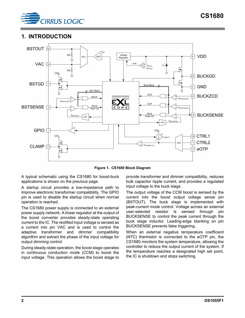
1. INTRODUCTION
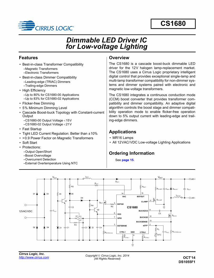
A typical schematic using the CS1680 for boost-buckapplications is shown on the previous page.
A startup circuit provides a low-impedance path toimprove electronic transformer compatibility. The GPIOpin is used to disable the startup circuit when normaloperation is reached.
The CS1680 power supply is connected to an externalpower supply network. A linear regulator at the output ofthe boost converter provides steady-state operatingcurrent to the IC. The rectified input voltage is sensed asa current into pin VAC and is used to control theadaptive transformer and dimmer compatibilityalgorithm and extract the phase of the input voltage foroutput dimming control.
During steady-state operation, the boost stage operatesin continuous conduction mode (CCM) to boost theinput voltage. This operation allows the boost stage to
provide transformer and dimmer compatibility, reducesbulk capacitor ripple current, and provides a regulatedinput voltage to the buck stage.
The output voltage of the CCM boost is sensed by thecurrent into the boost output voltage sense pin(BSTOUT). The buck stage is implemented withpeak-current mode control. Voltage across an externaluser-selected resistor is sensed through pinBUCKSENSE to control the peak current through thebuck stage inductor. Leading-edge blanking on pinBUCKSENSE prevents false triggering.
When an external negative temperature coefficient(NTC) thermistor is connected to the eOTP pin, theCS1680 monitors the system temperature, allowing thecontroller to reduce the output current of the system. Ifthe temperature reaches a designated high set point,the IC is shutdown and stops switching.
VZ
POR+
-
Voltage
Regulator6 VDD
13 BUCKSENSE+
-
9 BUCKZCD+
-
12 BUCKGD
VAC
DAC
+
-
ZCD
4 GND
15BSTOUT
OCP
11CLAMP
VST(th)
VSTP(th)
VBUCKOCP(th)
VBUCKZCD(th)
VBUCKPK(th)
ADC
Iref
5BSTGD
VDD
7GPIO
3BSTSENSE +
-
DAC
+
-
Boost
Peak Ctrl
BOCP
2
VBSTOCP(th)
VBSTPK(th)
+
-
ICONNECT
VCONNECT (th)
VDD
Buck
Peak Ctrl
MUX CTRL21
14
eOTP2
CTRL116
20k
20k
MUX
BST Blank
3Buck Blank
VDD
Figure 1. CS1680 Block Diagram
CS1680
DS1055F1 3
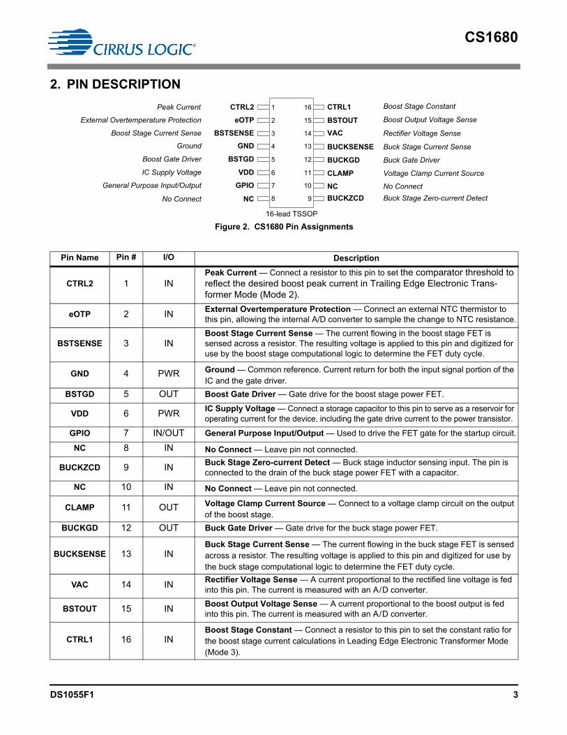
2. PIN DESCRIPTION
Pin Name Pin # I/O Description
CTRL2 1 INPeak Current — Connect a resistor to this pin to set the comparator threshold to reflect the desired boost peak current in Trailing Edge Electronic Trans-former Mode (Mode 2).
eOTP 2 INExternal Overtemperature Protection — Connect an external NTC thermistor to this pin, allowing the internal A/D converter to sample the change to NTC resistance.
BSTSENSE 3 INBoost Stage Current Sense — The current flowing in the boost stage FET is sensed across a resistor. The resulting voltage is applied to this pin and digitized for use by the boost stage computational logic to determine the FET duty cycle.
GND 4 PWR Ground — Common reference. Current return for both the input signal portion of the IC and the gate driver.
BSTGD 5 OUT Boost Gate Driver — Gate drive for the boost stage power FET.
VDD 6 PWRIC Supply Voltage — Connect a storage capacitor to this pin to serve as a reservoir for operating current for the device, including the gate drive current to the power transistor.
GPIO 7 IN/OUT General Purpose Input/Output — Used to drive the FET gate for the startup circuit.
NC 8 IN No Connect — Leave pin not connected.
BUCKZCD 9 INBuck Stage Zero-current Detect — Buck stage inductor sensing input. The pin is connected to the drain of the buck stage power FET with a capacitor.
NC 10 IN No Connect — Leave pin not connected.
CLAMP 11 OUT Voltage Clamp Current Source — Connect to a voltage clamp circuit on the output of the boost stage.
BUCKGD 12 OUT Buck Gate Driver — Gate drive for the buck stage power FET.
BUCKSENSE 13 INBuck Stage Current Sense — The current flowing in the buck stage FET is sensed across a resistor. The resulting voltage is applied to this pin and digitized for use by the buck stage computational logic to determine the FET duty cycle.
VAC 14 INRectifier Voltage Sense — A current proportional to the rectified line voltage is fed into this pin. The current is measured with an A/D converter.
BSTOUT 15 INBoost Output Voltage Sense — A current proportional to the boost output is fed into this pin. The current is measured with an A/D converter.
CTRL1 16 INBoost Stage Constant — Connect a resistor to this pin to set the constant ratio for the boost stage current calculations in Leading Edge Electronic Transformer Mode (Mode 3).
General Purpose Input/Output
Boost Gate Driver
Ground
Peak Current
External Overtemperature Protection
No Connect
GPIOVDDIC Supply Voltage
BSTGDGND
CTRL2
NCCLAMPBUCKGDBUCKSENSE
VACBSTOUT
CTRL1eOTP
BSTSENSEBoost Stage Current Sense
16-lead TSSOP
NC BUCKZCD7
6
5
4
3
2
1
10
11
12
13
14
15
16
8 9
No Connect
Voltage Clamp Current Source
Buck Gate Driver
Buck Stage Current Sense
Rectifier Voltage Sense
Boost Output Voltage Sense
Boost Stage Constant
Buck Stage Zero-current Detect
Figure 2. CS1680 Pin Assignments
CS1680
4 DS1055F1
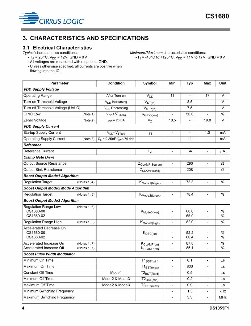
3. CHARACTERISTICS AND SPECIFICATIONS
3.1 Electrical CharacteristicsTypical characteristics conditions:
- TA = 25 °C, VDD = 12V, GND = 0 V- All voltages are measured with respect to GND.- Unless otherwise specified, all currents are positive when flowing into the IC.
Minimum/Maximum characteristics conditions:- TJ = -40°C to +125 °C, VDD = 11V to 17V, GND = 0 V
Parameter Condition Symbol Min Typ Max Unit
VDD Supply Voltage
Operating Range After Turn-on VDD 11 - 17 V
Turn-on Threshold Voltage VDD Increasing VST(th) - 8.5 - V
Turn-off Threshold Voltage (UVLO) VDD Decreasing VSTP(th) - 7.5 - V
GPIO Low (Note 1) VDD >VST(th) KGPIO(low) - 50.0 - %
Zener Voltage (Note 2) IDD = 20mA VZ 18.5 - 19.8 V
VDD Supply Current
Startup Supply Current VDD<VST(th) IST - - 1.0 mA
Operating Supply Current (Note 3) CL = 0.25nF, fsw 70 kHz - 11 - mA
Reference
Reference Current Iref - 64 - A
Clamp Gate Drive
Output Source Resistance ZCLAMP(Source) - 290 -
Output Sink Resistance ZCLAMP(Sink) - 208 -
Boost Output Mode1 Algorithm
Regulation Target (Notes 1, 4) KMode1(target) - 73.3 - %
Boost Output Mode2 Mode Algorithm
Regulation Target (Notes 1, 5) KMode2(target) - 78.4 - %
Boost Output Mode3 Algorithm
Regulation Range Low (Notes 1, 6)CS1680-00CS1680-02
KMode3(low) --
60.065.9
--
%%
Regulation Range High (Notes 1, 6) KMode3(high) - 82.0 - %
Accelerated Decrease OnCS1680-00CS1680-02
KDEC(on) --
52.260.4
--
%%
Accelerated Increase On (Notes 1, 7)Accelerated Increase Off (Notes 1, 7)
KCLAMP(on)KCLAMP(off)
--
87.885.1
--
%%
Boost Pulse Width Modulator
Minimum On Time T1BST(min) - 0.1 - s
Maximum On Time T1BST(max) - 800 - s
Constant Off Time Mode1 T2BST(fixed) - 0.5 - s
Minimum Off Time Mode2 & Mode3 T2BST(min) - 0.2 - s
Maximum Off Time Mode2 & Mode3 T2BST(max) - 0.9 - s
Minimum Switching Frequency - 1.3 - kHz
Maximum Switching Frequency - 3.3 - MHz
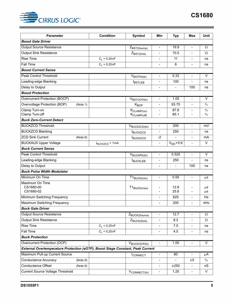
CS1680
DS1055F1 5
Boost Gate Driver
Output Source Resistance ZBST(Source) - 19.9 -
Output Sink Resistance ZBST(Sink) - 10.5 -
Rise Time CL = 0.25nF - 11 - ns
Fall Time CL = 0.25nF - 6 - ns
Boost Current Sense
Peak Control Threshold VBSTPK(th) - 0.33 - V
Leading-edge Blanking tBSTLEB - 100 - ns
Delay to Output - - 100 ns
Boost Protection
Overcurrent Protection (BOCP) VBSTOCP(th) - 1.05 - V
Overvoltage Protection (BOP) (Note 1) KBOP - 93.75 -
Clamp Turn-onClamp Turn-off
KCLAMP(on)KCLAMP(off)
--
87.885.1
--
Buck Zero-Current Detect
BUCKZCD Threshold VBUCKZCD(th) - 200 - mV
BUCKZCD Blanking tBUCKZCD - 250 - ns
ZCD Sink Current (Note 8) IBUCKZCD -2 - - mA
BUCKAUX Upper Voltage IBUCKZCD = 1mA - VDD+0.6 - V
Buck Current Sense
Peak Control Threshold VBUCKPK(th) - 0.525 - V
Leading-edge Blanking tBUCKLEB - 250 - ns
Delay to Output - - 100 ns
Buck Pulse Width Modulator
Minimum On Time T1BUCK(min) - 0.55 - s
Maximum On TimeCS1680-00CS1680-02
T1BUCK(max) --
12.825.6
--
ss
Minimum Switching Frequency - 625 - Hz
Maximum Switching Frequency - 200 - kHz
Buck Gate Driver
Output Source Resistance ZBUCK(Source) - 12.7 -
Output Sink Resistance ZBUCK(Sink) - 8.2 -
Rise Time CL = 0.25nF - 7.0 - ns
Fall Time CL = 0.25nF - 4.5 - ns
Buck Protection
Overcurrent Protection (OCP) VBUCKOCP(th) - 1.05 - V
External Overtemperature Protection (eOTP), Boost Stage Constant, Peak Current
Maximum Pull-up Current Source ICONNECT - 80 - A
Conductance Accuracy (Note 9) - - ±5
Conductance Offset (Note 9) - ±250 - nS
Current Source Voltage Threshold VCONNECT(th) - 1.25 - V
Parameter Condition Symbol Min Typ Max Unit
CS1680
6 DS1055F1
Notes: 1. Threshold is characterized as a percentage of the full-scale boost output voltage, VBST(full)2. The CS1680 has an internal shunt regulator that limits the voltage on the VDD pin. VZ, the shunt regulation voltage, is defined in
the VDD Supply Voltage section on page 4.3. For test purposes, load capacitance CL is connected to gate drive pins and is equal to 0.25nF.4. Mode1 algorithm regulates value at the trough of the rectified waveform.5. Mode2 algorithm regulates boost output voltage at the phase cut of each rectified waveform.6. LED output current begins changing if boost output voltage is outside the Mode3 algorithm regulation range.7. Accelerated increase in LED output current begins at clamp on and continues until the boost output voltage falls to clamp off.8. External circuitry should be designed to ensure that the ZCD current drawn from the internal clamp diode when it is forward biased
does not exceed specification.9. The conductance is specified in Siemens (S or 1/). Each LSB of the internal ADC corresponds to 250nS or one parallel 4M
resistor. Full scale corresponds to 256 parallel 4M resistors or 15.625k. 10. Specifications are guaranteed by design and are characterized and correlated using statistical process methods.
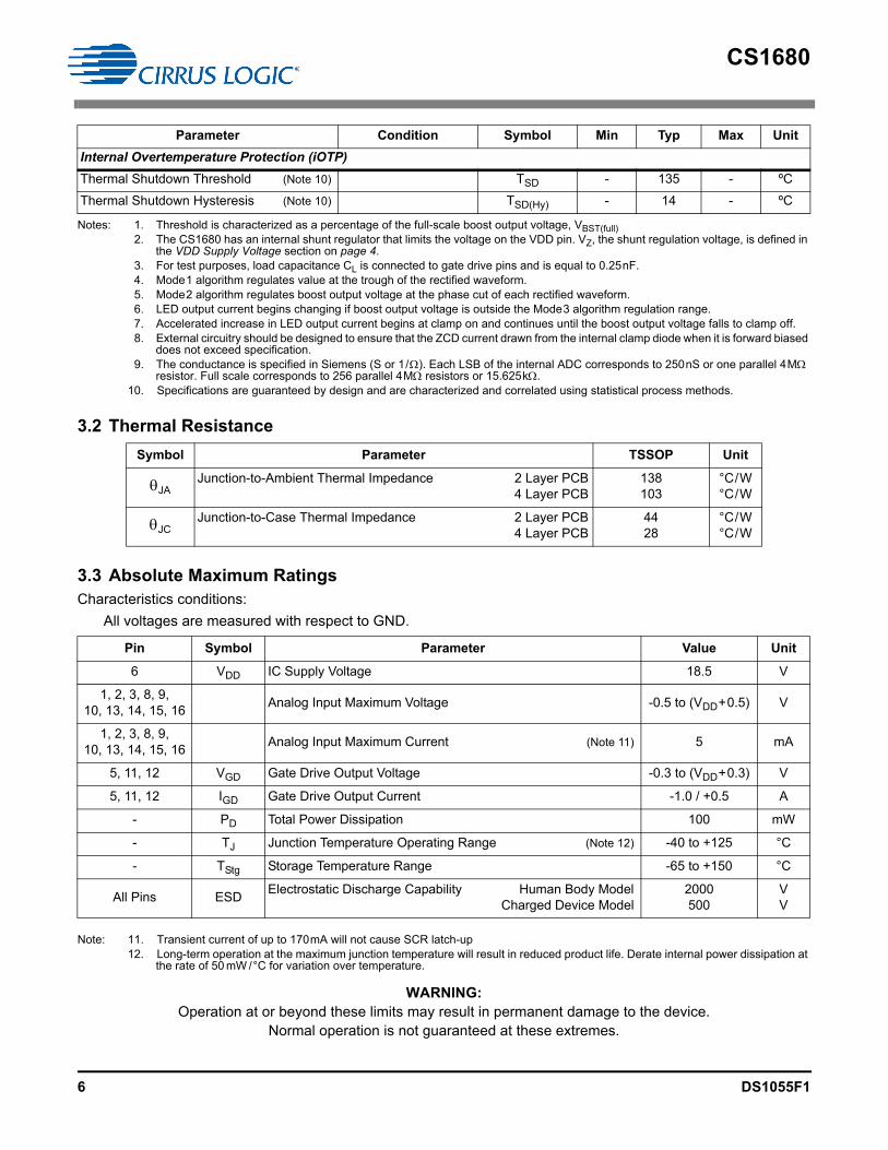
3.2 Thermal Resistance
3.3 Absolute Maximum RatingsCharacteristics conditions:
All voltages are measured with respect to GND.
Note: 11. Transient current of up to 170mA will not cause SCR latch-up12. Long-term operation at the maximum junction temperature will result in reduced product life. Derate internal power dissipation at
the rate of 50 mW /°C for variation over temperature.
WARNING:Operation at or beyond these limits may result in permanent damage to the device.
Normal operation is not guaranteed at these extremes.
Internal Overtemperature Protection (iOTP)
Thermal Shutdown Threshold (Note 10) TSD - 135 - ºC
Thermal Shutdown Hysteresis (Note 10) TSD(Hy) - 14 - ºC
Symbol Parameter TSSOP Unit
JAJunction-to-Ambient Thermal Impedance 2 Layer PCB
4 Layer PCB138103
°C/W°C/W
JCJunction-to-Case Thermal Impedance 2 Layer PCB
4 Layer PCB4428
°C/W°C/W
Pin Symbol Parameter Value Unit
6 VDD IC Supply Voltage 18.5 V
1, 2, 3, 8, 9,10, 13, 14, 15, 16
Analog Input Maximum Voltage -0.5 to (VDD+0.5) V
1, 2, 3, 8, 9,10, 13, 14, 15, 16
Analog Input Maximum Current (Note 11) 5 mA
5, 11, 12 VGD Gate Drive Output Voltage -0.3 to (VDD+0.3) V
5, 11, 12 IGD Gate Drive Output Current -1.0 / +0.5 A
- PD Total Power Dissipation 100 mW
- TJ Junction Temperature Operating Range (Note 12) -40 to +125 °C
- TStg Storage Temperature Range -65 to +150 °C
All Pins ESDElectrostatic Discharge Capability Human Body Model
Charged Device Model2000500
VV
Parameter Condition Symbol Min Typ Max Unit
CS1680
DS1055F1 7
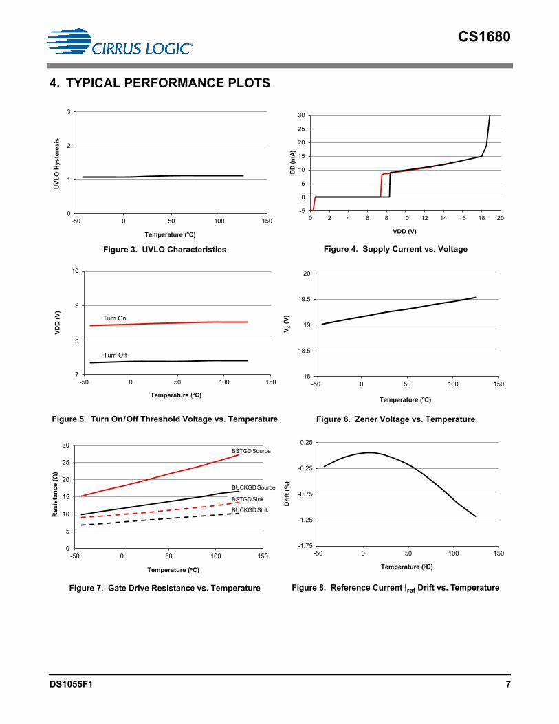
4. TYPICAL PERFORMANCE PLOTS
Figure 3. UVLO Characteristics Figure 4. Supply Current vs. Voltage
Figure 5. Turn On/Off Threshold Voltage vs. Temperature Figure 6. Zener Voltage vs. Temperature
Figure 7. Gate Drive Resistance vs. Temperature Figure 8. Reference Current Iref Drift vs. Temperature
0
1
2
3
-50 0 50 100 150
UVL
O H
yste
resi
s
Temperature (ºC)
-5
0
5
10
15
20
25
30
0 2 4 6 8 10 12 14 16 18 20
IDD
(mA)
VDD (V)
7
8
9
10
-50 0 50 100 150
VDD
(V)
Temperature (ºC)
Turn Off
Turn On
18
18.5
19
19.5
20
-50 0 50 100 150
V Z(V
)
Temperature (ºC)
0
5
10
15
20
25
30
-50 0 50 100 150
Res
ista
nce
()
Temperature (oC)
BSTGD Source
BUCKGDSource
BSTGD Sink
BUCKGDSink
-1.75
-1.25
-0.75
-0.25
0.25
-50 0 50 100 150
Drif
t (%
)
Temperature (�C)
CS1680
8 DS1055F1
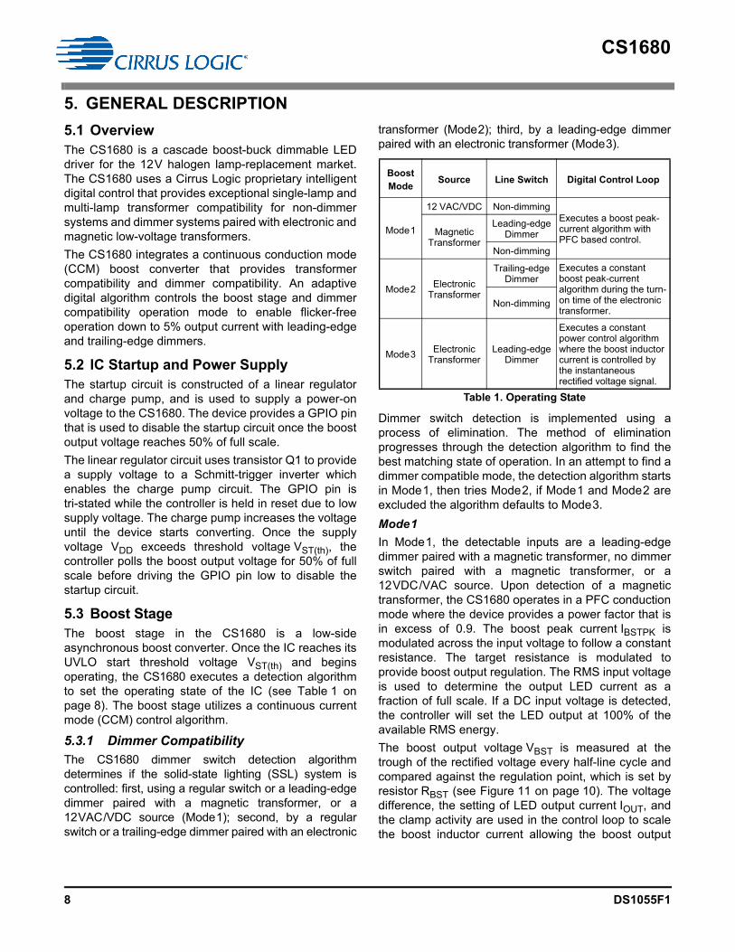
5. GENERAL DESCRIPTION
5.1 OverviewThe CS1680 is a cascade boost-buck dimmable LEDdriver for the 12V halogen lamp-replacement market.The CS1680 uses a Cirrus Logic proprietary intelligentdigital control that provides exceptional single-lamp andmulti-lamp transformer compatibility for non-dimmersystems and dimmer systems paired with electronic andmagnetic low-voltage transformers.
The CS1680 integrates a continuous conduction mode(CCM) boost converter that provides transformercompatibility and dimmer compatibility. An adaptivedigital algorithm controls the boost stage and dimmercompatibility operation mode to enable flicker-freeoperation down to 5% output current with leading-edgeand trailing-edge dimmers.
5.2 IC Startup and Power SupplyThe startup circuit is constructed of a linear regulatorand charge pump, and is used to supply a power-onvoltage to the CS1680. The device provides a GPIO pinthat is used to disable the startup circuit once the boostoutput voltage reaches 50% of full scale.
The linear regulator circuit uses transistor Q1 to providea supply voltage to a Schmitt-trigger inverter whichenables the charge pump circuit. The GPIO pin istri-stated while the controller is held in reset due to lowsupply voltage. The charge pump increases the voltageuntil the device starts converting. Once the supplyvoltage VDD exceeds threshold voltage VST(th), thecontroller polls the boost output voltage for 50% of fullscale before driving the GPIO pin low to disable thestartup circuit.
5.3 Boost StageThe boost stage in the CS1680 is a low-sideasynchronous boost converter. Once the IC reaches itsUVLO start threshold voltage VST(th) and beginsoperating, the CS1680 executes a detection algorithmto set the operating state of the IC (see Table 1 onpage 8). The boost stage utilizes a continuous currentmode (CCM) control algorithm.
5.3.1 Dimmer Compatibility
The CS1680 dimmer switch detection algorithmdetermines if the solid-state lighting (SSL) system iscontrolled: first, using a regular switch or a leading-edgedimmer paired with a magnetic transformer, or a12VAC/VDC source (Mode1); second, by a regularswitch or a trailing-edge dimmer paired with an electronic
transformer (Mode2); third, by a leading-edge dimmerpaired with an electronic transformer (Mode3).
Dimmer switch detection is implemented using aprocess of elimination. The method of eliminationprogresses through the detection algorithm to find thebest matching state of operation. In an attempt to find adimmer compatible mode, the detection algorithm startsin Mode1, then tries Mode2, if Mode1 and Mode2 areexcluded the algorithm defaults to Mode3.
Mode1
In Mode1, the detectable inputs are a leading-edgedimmer paired with a magnetic transformer, no dimmerswitch paired with a magnetic transformer, or a12VDC/VAC source. Upon detection of a magnetictransformer, the CS1680 operates in a PFC conductionmode where the device provides a power factor that isin excess of 0.9. The boost peak current IBSTPK ismodulated across the input voltage to follow a constantresistance. The target resistance is modulated toprovide boost output regulation. The RMS input voltageis used to determine the output LED current as afraction of full scale. If a DC input voltage is detected,the controller will set the LED output at 100% of theavailable RMS energy.
The boost output voltage VBST is measured at thetrough of the rectified voltage every half-line cycle andcompared against the regulation point, which is set byresistor RBST (see Figure 11 on page 10). The voltagedifference, the setting of LED output current IOUT, andthe clamp activity are used in the control loop to scalethe boost inductor current allowing the boost output
Boost Mode
Source Line Switch Digital Control Loop
Mode1
12 VAC/VDC Non-dimmingExecutes a boost peak-current algorithm with PFC based control.
Magnetic Transformer
Leading-edge Dimmer
Non-dimming
Mode2Electronic
Transformer
Trailing-edge Dimmer
Executes a constant boost peak-current algorithm during the turn-on time of the electronic transformer.
Non-dimming
Mode3 Electronic Transformer
Leading-edge Dimmer
Executes a constant power control algorithm where the boost inductor current is controlled by the instantaneous rectified voltage signal.
Table 1. Operating State
CS1680
DS1055F1 9
voltage to reach the regulation target set byconstant KMode1(target). If boost output voltage VBST isbelow the target regulation point or the boost outputvoltage is falling, the boost inductor current is increased.If the boost output voltage is above the target regulationpoint, the boost output voltage is rising, or the clamp hasbeen activated recently the boost current is decreased.The LED output current is set using a third-orderpolynomial of the rectified RMS voltage, computed overa half-line cycle and filtered to avoid lamp flicker.
Mode2
In Mode2, the CS1680 will detect if the input is a trailingedge dimmer paired with an electronic transformer or nodimmer switch paired with an electronic transformer. Thedetection algorithm determines its operation based onthe falling edge of the input voltage waveform. To provideproper dimmer operation, the CS1680 executes theboost algorithm on the falling edge of the input linevoltage, which will maintain a charge in the dimmercapacitor. To ensure maximum compatibility with dimmercomponents, the device boosts during this falling edgeevent using a peak current that must meet a minimumvalue.
The boost output voltage VBST is measured at thetrailing edge of the rectified voltage every half-line cycleand compared against the regulation point, which is setby resistor RBST (see Figure 11 on page 10). Thevoltage difference, the setting of LED outputcurrent IOUT, and the clamp activity are used in thecontrol loop to modulate the boost turn-on time everyhalf-line cycle which allows the boost output voltage toreach the regulation target set by constantKMode2(target). If boost output voltage VBST is below thetarget regulation point or the boost output voltage isfalling, the total turn-on time over a half-line cycle isincreased. If the boost output voltage is above the targetregulation point, the boost output voltage is rising, or theclamp has been activated recently, the total turn-on timeover a half-line cycle is decreased. The Mode2algorithm estimates the turn-on time of the transformerby measuring the conduction angle of the rectifiedvoltage every half-line cycle. The LED output current isset based on the output power requirements for aparticular conduction angle by the regulation loop.
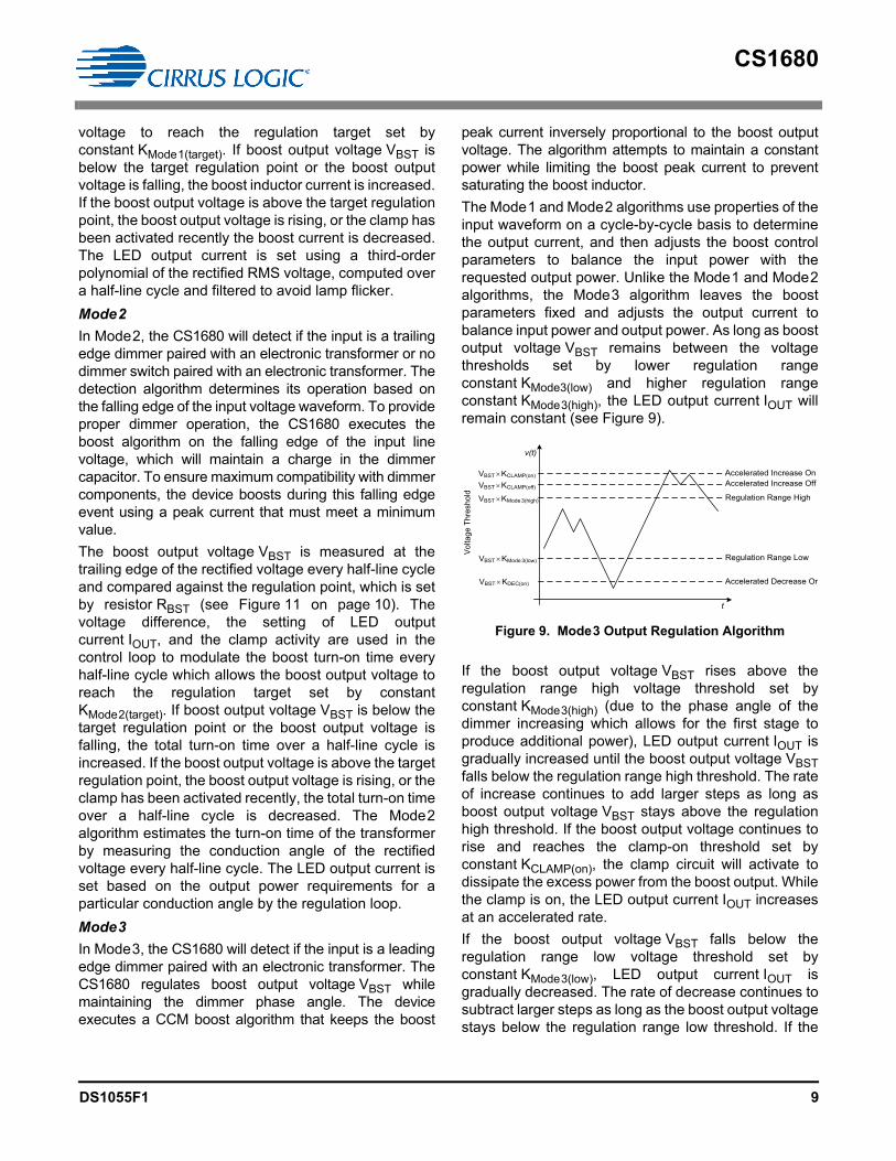
Mode3
In Mode3, the CS1680 will detect if the input is a leadingedge dimmer paired with an electronic transformer. TheCS1680 regulates boost output voltage VBST whilemaintaining the dimmer phase angle. The deviceexecutes a CCM boost algorithm that keeps the boost
peak current inversely proportional to the boost outputvoltage. The algorithm attempts to maintain a constantpower while limiting the boost peak current to preventsaturating the boost inductor.
The Mode1 and Mode2 algorithms use properties of theinput waveform on a cycle-by-cycle basis to determinethe output current, and then adjusts the boost controlparameters to balance the input power with therequested output power. Unlike the Mode1 and Mode2algorithms, the Mode3 algorithm leaves the boostparameters fixed and adjusts the output current tobalance input power and output power. As long as boostoutput voltage VBST remains between the voltagethresholds set by lower regulation rangeconstant KMode3(low) and higher regulation rangeconstant KMode3(high), the LED output current IOUT willremain constant (see Figure 9).
If the boost output voltage VBST rises above theregulation range high voltage threshold set byconstant KMode3(high) (due to the phase angle of thedimmer increasing which allows for the first stage toproduce additional power), LED output current IOUT isgradually increased until the boost output voltage VBSTfalls below the regulation range high threshold. The rateof increase continues to add larger steps as long asboost output voltage VBST stays above the regulationhigh threshold. If the boost output voltage continues torise and reaches the clamp-on threshold set byconstant KCLAMP(on), the clamp circuit will activate todissipate the excess power from the boost output. Whilethe clamp is on, the LED output current IOUT increasesat an accelerated rate.
If the boost output voltage VBST falls below theregulation range low voltage threshold set byconstant KMode3(low), LED output current IOUT isgradually decreased. The rate of decrease continues tosubtract larger steps as long as the boost output voltagestays below the regulation range low threshold. If the
Regulation Range High
Regulation Range Low
Accelerated Decrease On
Accelerated Increase On
Accelerated Increase Off
VBST KMode 3(high)
VBST KCLAMP(off)
VBST KCLAMP(on)
VBST KMode 3(low)
VBST KDEC(on)
t
v(t)
Voltage T
hre
shold
Figure 9. Mode3 Output Regulation Algorithm
CS1680
10 DS1055F1
boost output voltage continues to fall and reaches thelowest threshold set by constant KDEC(on), the LEDoutput current is decreased at an accelerated rate.
If the LED output current IOUT is at a maximum andboost output voltage VBST is still above the regulationhigh threshold, the controller begins scaling down theboost inductor current instead of increasing the LEDoutput current. If this happens, when the boost outputvoltage falls below the regulation low threshold, theboost input current is gradually increased back tonominal before the LED output current begins to reduceoff from the maximum.
5.3.2 Boost Stage Control
The boost stage uses continuous conduction modeoperation for high compatibility with electronictransformers. For current regulation, the controllervaries the peak current IBSTPK as necessary for dimmerand transformer compatibility. When the dimmer ispaired with an electronic transformer, period T2BST ismodulated to maintain a constant ripple current on theboost inductor. When the dimmer is paired with amagnetic transformer, the demagnetization period hasa constant T2BST(fixed) time.
Maximum Peak Current
The maximum boost inductor peak current IBSTPK(max)is set using the current sense resistor RBST(Sense) onpin BSTSENSE, which is sampled by a comparatorreferenced to an internal DAC. Boost peak currentIBSTPK(max) is calculated using Equation 1:
Boost overcurrent protection (BOCP) is provided usinga higher threshold to detect the event of inductorsaturation. If the voltage on the BSTSENSE pinexceeds a threshold voltage VBSTOCP(th) of 1.05V, thecontroller enters a BOCP fault. The IC output isdisabled, the gate drive output pins BSTGD andBUCKGD turn off, and the controller attempts to restart
after one second. The boost overcurrent protectioncurrent IBSTPK(OCP) is calculated using Equation 2:
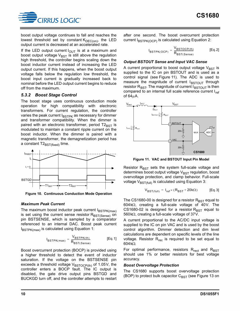
Output BSTOUT Sense and Input VAC Sense
A current proportional to boost output voltage VBST issupplied to the IC on pin BSTOUT and is used as acontrol signal (see Figure 11). The ADC is used tomeasure the magnitude of current IBSTOUT throughresistor RBST. The magnitude of current IBSTOUT is thencompared to an internal full scale reference current Irefof 64A.
Resistor RBST sets the system full-scale voltage anddetermines boost output voltage VBST regulation, boostovervoltage protection, and clamp behavior. Full-scalevoltage VBST(full) is calculated using Equation 3:
The CS1680-00 is designed for a resistor RBST equal to604k, creating a full-scale voltage of 40V. TheCS1680-02 is designed for a resistor RBST equal to560k, creating a full-scale voltage of 37V.
A current proportional to the AC/DC input voltage issupplied to the IC on pin VAC and is used by the boostcontrol algorithm. Dimmer detection and dim levelcalculations are dependent on specific levels of the linevoltage. Resistor Rrec is required to be set equal to604kFor optimal performance, resistors Rrect and RBSTshould use 1% or better resistors for best voltageaccuracy.
Boost Overvoltage Protection
The CS1680 supports boost overvoltage protection(BOP) to protect bulk capacitor CBST (see Figure 13 on
T1BSTi T2BSTi
BSTGD
IL
IPKBST
IL = 0
Figure 10. Continuous Conduction Mode Operation
IBSTPK max VBSTPK th
RBST Sense ---------------------------------= [Eq.1]
IBSTPK OCP VBSTOCP th RBST Sense ---------------------------------= [Eq.2]
DBST
Vrect VBST
Rrect
CS1680
IBSTOUT
BSTOUT
VAC
ADC
Iref
20k
20k
MUX
15
14
IVAC
RBST
LBST
Figure 11. VAC and BSTOUT Input Pin Model
VBST full Iref RBST 20k+ = [Eq.3]
CS1680
DS1055F1 11
page 11). If the boost output voltage exceeds theovervoltage protection threshold, a BOP fault signal isgenerated. Boost overvoltage threshold VBOP(th) iscalculated using Equation 4:
For a nominal system design where resistor RBSTequals 604k and full-scale voltage VBST(full) equals40V, this sets threshold voltage VBOP(th) to 37.4V.
The control logic continuously averages this BOP faultsignal, and if at any point in time the average exceeds aset event threshold, the boost stage is disabled.
5.3.3 Voltage Clamp CircuitDuring transient events and interactions with electronictransformers, it is possible for the boost stage togenerate more power than is consumed by the secondstage. A clamping circuit is added to the system todissipate the excess power. The CS1680 providesactive clamp circuitry on pin CLAMP, as shown inFigure 12.
The clamp circuit is enabled when boost outputvoltage VBST exceeds the clamp turn-on thresholdvoltage VCLAMP(on). The clamp circuit will remain turnedon until boost output voltage VBST is lowered below theclamp turn-off threshold voltage VCLAMP(off). Thresholdvoltage VCLAMP(on) is calculated using Equation 5:
Threshold voltage VCLAMP(off) is calculated usingEquation 6:
Clamp Overpower Protection
The CS1680 clamp overpower protection (COP) controllogic continuously monitors the turn-on time of the
clamp circuit. If the cumulative turn-on time exceeds200ms during the internally generated 2-secondwindow time, a COP event is actuated, disabling theboost and buck stages. The clamp circuitry is turned offduring the fault event.
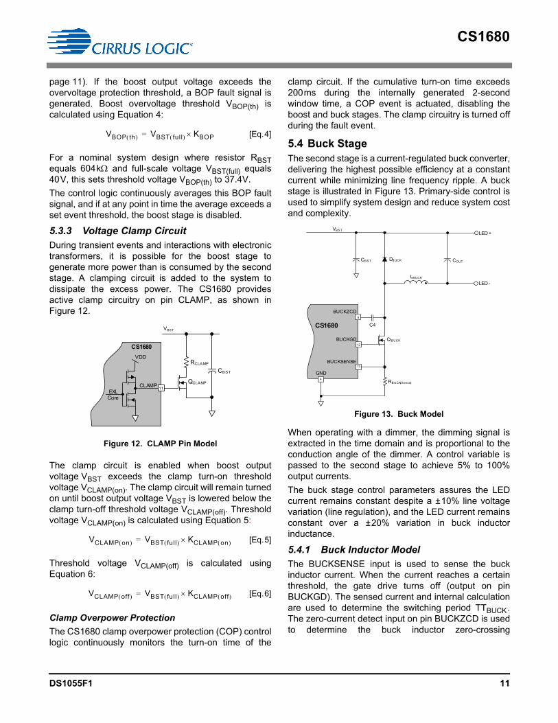
5.4 Buck StageThe second stage is a current-regulated buck converter,delivering the highest possible efficiency at a constantcurrent while minimizing line frequency ripple. A buckstage is illustrated in Figure 13. Primary-side control isused to simplify system design and reduce system costand complexity.
When operating with a dimmer, the dimming signal isextracted in the time domain and is proportional to theconduction angle of the dimmer. A control variable ispassed to the second stage to achieve 5% to 100%output currents.
The buck stage control parameters assures the LEDcurrent remains constant despite a ±10% line voltagevariation (line regulation), and the LED current remainsconstant over a ±20% variation in buck inductorinductance.
5.4.1 Buck Inductor ModelThe BUCKSENSE input is used to sense the buckinductor current. When the current reaches a certainthreshold, the gate drive turns off (output on pinBUCKGD). The sensed current and internal calculationare used to determine the switching period TTBUCK.The zero-current detect input on pin BUCKZCD is usedto determine the buck inductor zero-crossing
VBOP th VBST full KBOP= [Eq.4]
CLAMP
RCLAMP
VBST
CS1680
11
CB ST
VDD
EXLCore
QCLAMP
Figure 12. CLAMP Pin Model
VCLAMP on VBST full KCLAMP on = [Eq.5]
VCLAMP off VBST full KCLAMP off = [Eq.6]
GND
BUCKGD
BUCKSENSE
CS1680
RBUCK(Sense)
QBUCK
LED +
LED -
VBST
CBST DBUCK COUT
13
12
4
C4
BUCKZCD9
LBUCK
Figure 13. Buck Model
CS1680
12 DS1055F1
period T2BUCK. The controller then uses thetime TTBUCK to determine gate turn-on time.
5.4.2 Current Sense Resistor Model
The digital algorithm ensures monotonic dimming from5% to 100% of the dimming range with a linearrelationship between the dimming signal and the LEDcurrent. The buck stage is regulated by peak currentcontrol with a 1% external sense resistor RBUCK(Sense)connected to the BUCKSENSE pin. Buck peak currentIBUCKPK(max) is calculated using Equation 7:
Overcurrent protection (OCP) is implemented bymonitoring the voltage across buck senseresistor RBUCK(Sense). If this voltage exceeds athreshold voltage VBUCKOCP(th) of 1.05 V, a faultcondition occurs. The IC output is disabled, the gatedrive output pins BSTGD and BUCKGD turn off, and thecontroller attempts to restart after one second. The buckovercurrent protection current IBUCKPK(OCP) iscalculated using Equation 8:
5.4.3 Zero-current Detection
Zero-current switching is achieved by detecting thebuck inductor current zero-crossing using a capacitivecoupling network. The digital control algorithm rejectsline-frequency ripple created on the second-stage inputby the front-end boost stage, resulting in the highestpossible LED efficiency and long LED life.
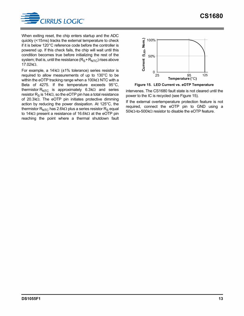
5.5 Overtemperature ProtectionThe CS1680 incorporates both internal overtemperatureprotection (iOTP) and the ability to connect an externalovertemperature sense circuit for IC protection. Typical-ly, a negative temperature coefficient (NTC) thermistor isused.
5.5.1 Internal Overtemperature Protection
Internal overtemperature protection (iOTP) is activated,and switching is disabled when the die temperature ofthe devices exceeds 135°C. There is a hysteresis ofabout 14°C before resuming normal operation.
5.5.2 External Overtemperature Protection
The external overtemperature protection (eOTP) pin isused to implement overtemperature protection. A negative
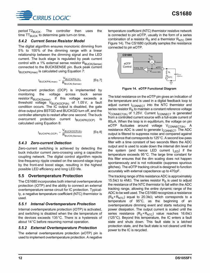
temperature coefficient (NTC) thermistor resistive networkis connected to pin eOTP, usually in the form of a seriescombination of a resistor RS and a thermistor RNTC (seeFigure 14). The CS1680 cyclically samples the resistanceconnected to pin eOTP.
The total resistance on the eOTP pin gives an indication ofthe temperature and is used in a digital feedback loop toadjust current ICONNECT into the NTC thermistor andseries resistor RS to maintain a constant reference voltageVCONNECT(th) of 1.25V. Current ICONNECT is generatedfrom a controlled current source with a full-scale current of80A. When the loop is in equilibrium, the voltage on pineOTP fluctuates around voltage VCONNECT(th). Aresistance ADC is used to generate ICONNECT. The ADCoutput is filtered to suppress noise and compared againsta reference that corresponds to 125°C. A second low-passfilter with a time constant of two seconds filters the ADCoutput and is used to scale down the internal dim level ofthe system (and hence LED current ILED) if thetemperature exceeds 95°C. The large time constant forthis filter ensures that the dim scaling does not happenspontaneously and is not noticeable (suppress spuriousglitches). The eOTP tracking circuit is designed to functionaccurately with external capacitance up to 470pF.
The tracking range of this resistance ADC is approximately15.5k to 4M. The series resistor RS is used to adjustthe resistance of the NTC thermistor to fall within the ADCtracking range, allowing the entire dynamic range of theADC to be well used. The CS1680 recognizes a resistance(RS+RNTC) equal to 20.3k which corresponds to atemperature of 95°C, as the beginning of anovertemperature dimming event and starts reducing thepower dissipation. The output current is scaled until theseries resistance (RS+RNTC) value reaches 16.6k(125°C). Beyond this temperature, the IC enters a faultstate and shuts down. This fault state is a latchedprotection state, and the fault state is not cleared until thepower to the IC is recycled.
IBUCKPK max VBUCKPK th
RBUCK Sense -------------------------------------= [Eq.7]
IBUCKPK OCP VBUCKOCP th RBUCK Sense -------------------------------------= [Eq.8]
CS1680
+-
ICONNECT
VCONNECT(th)
Comp_Out
eOTP Control eOTP
RS
CNTC
NTC
VDD
2
(Optional )
Figure 14. eOTP Functional Diagram
CS1680
DS1055F1 13
When exiting reset, the chip enters startup and the ADCquickly (<15ms) tracks the external temperature to checkif it is below 120°C reference code before the controller ispowered up. If this check fails, the chip will wait until thiscondition becomes true before initializing the rest of thesystem; that is, until the resistance (RS+RNTC) rises above17.02k.
For example, a 14k (±1% tolerance) series resistor isrequired to allow measurements of up to 130°C to bewithin the eOTP tracking range when a 100k NTC with aBeta of 4275. If the temperature exceeds 95°C,thermistor RNTC is approximately 6.3k and seriesresistor RS is 14k, so the eOTP pin has a total resistanceof 20.3k. The eOTP pin initiates protective dimmingaction by reducing the power dissipation. At 125°C, thethermistor RNTC has 2.6k plus a series resistor RS equalto 14k present a resistance of 16.6k at the eOTP pinreaching the point where a thermal shutdown fault
intervenes. The CS1680 fault state is not cleared until thepower to the IC is recycled (see Figure 15).
If the external overtemperature protection feature is notrequired, connect the eOTP pin to GND using a50k-to-500k resistor to disable the eOTP feature.
Temperature (°C)
Cu
rre
nt
(I L
ED,
No
m.)
12595
50%
100%
025
Figure 15. LED Current vs. eOTP Temperature
CS1680
14 DS1055F1
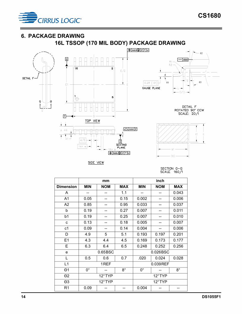
6. PACKAGE DRAWING
mm inch
Dimension MIN NOM MAX MIN NOM MAX
A -- -- 1.1 -- -- 0.043
A1 0.05 -- 0.15 0.002 -- 0.006
A2 0.85 -- 0.95 0.033 -- 0.037
b 0.19 -- 0.27 0.007 -- 0.011
b1 0.19 -- 0.25 0.007 -- 0.010
c 0.13 -- 0.18 0.005 -- 0.007
c1 0.09 -- 0.14 0.004 -- 0.006
D 4.9 5 5.1 0.193 0.197 0.201
E1 4.3 4.4 4.5 0.169 0.173 0.177
E 6.3 6.4 6.5 0.248 0.252 0.256
e 0.65BSC 0.026BSC
L 0.5 0.6 0.7 .020 0.024 0.028
L1 1REF 0.039REF
Θ1 0° -- 8° 0° -- 8°
Θ2 12°TYP 12°TYP
Θ3 12°TYP 12°TYP
R1 0.09 -- -- 0.004 -- --
16L TSSOP (170 MIL BODY) PACKAGE DRAWING
CS1680
DS1055F1 15
Notes:
1. Controlling dimensions are in millimeters.2. Dimensions and tolerances per ASME Y14.5M.3. This drawing conforms to JEDEC outline MS-012, variation AC for standard 16L TSSOP narrow body.4. Recommended reflow profile is per JEDEC/IPC J-STD-020.
7. ORDERING INFORMATION
8. ENVIRONMENTAL, MANUFACTURING, & HANDLING INFORMATION
a. MSL (Moisture Sensitivity Level) as specified by IPC/JEDEC J-STD-020.b. Stored at 30°C, 60% relative humidity.
R2 0.09 -- -- 0.004 -- --
S 0.2 -- -- 0.008 - --
aaa 0.2 0.008
bbb 0.1 0.004
ccc 0.1 0.004
ddd 0.05 0.002
mm inch
Dimension MIN NOM MAX MIN NOM MAX
Ordering Number AC Line Voltage Temperature Package DescriptionConfiguration
Version
CS1680-FZZ Bulk12VAC/VDC -40 °C to +125 °C
16-lead TSSOP,Lead (Pb) Free
3.09.1
CS1680-FZZR Tape & Reel 3.09.1
CS168002-FZZ Bulk12VAC/VDC -40 °C to +125 °C
16-lead TSSOP,Lead (Pb) Free
3.07.2
CS168002-FZZR Tape & Reel 3.07.2
Part Number Peak Reflow Temp MSL Ratinga Max Floor Lifeb
CS1680-FZZ 260 °C 3 7 Days
CS168002-FZZ 260 °C 3 7 Days
CS1680
16 DS1055F1
REVISION HISTORY
Contacting Cirrus Logic SupportFor all product questions and inquiries contact a Cirrus Logic Sales Representative. To find one nearest you go to http://www.cirrus.com
IMPORTANT NOTICE
Cirrus Logic, Inc. and its subsidiaries (“Cirrus”) believe that the information contained in this document is accurate and reliable. However, the information is subjectto change without notice and is provided “AS IS” without warranty of any kind (express or implied). Customers are advised to obtain the latest version of relevantinformation to verify, before placing orders, that information being relied on is current and complete. All products are sold subject to the terms and conditions of salesupplied at the time of order acknowledgment, including those pertaining to warranty, indemnification, and limitation of liability. No responsibility is assumed by Cirrusfor the use of this information, including use of this information as the basis for manufacture or sale of any items, or for infringement of patents or other rights of thirdparties. This document is the property of Cirrus and by furnishing this information, Cirrus grants no license, express or implied under any patents, mask work rights,copyrights, trademarks, trade secrets or other intellectual property rights. Cirrus owns the copyrights associated with the information contained herein and gives con-sent for copies to be made of the information only for use within your organization with respect to Cirrus integrated circuits or other products of Cirrus. This consentdoes not extend to other copying such as copying for general distribution, advertising or promotional purposes, or for creating any work for resale.
CERTAIN APPLICATIONS USING SEMICONDUCTOR PRODUCTS MAY INVOLVE POTENTIAL RISKS OF DEATH, PERSONAL INJURY, OR SEVERE PROP-ERTY OR ENVIRONMENTAL DAMAGE (“CRITICAL APPLICATIONS”). CIRRUS PRODUCTS ARE NOT DESIGNED, AUTHORIZED OR WARRANTED FOR USEIN PRODUCTS SURGICALLY IMPLANTED INTO THE BODY, AUTOMOTIVE SAFETY OR SECURITY DEVICES, LIFE SUPPORT PRODUCTS OR OTHER CRIT-ICAL APPLICATIONS. INCLUSION OF CIRRUS PRODUCTS IN SUCH APPLICATIONS IS UNDERSTOOD TO BE FULLY AT THE CUSTOMER'S RISK AND CIR-RUS DISCLAIMS AND MAKES NO WARRANTY, EXPRESS, STATUTORY OR IMPLIED, INCLUDING THE IMPLIED WARRANTIES OF MERCHANTABILITY ANDFITNESS FOR PARTICULAR PURPOSE, WITH REGARD TO ANY CIRRUS PRODUCT THAT IS USED IN SUCH A MANNER. IF THE CUSTOMER OR CUSTOM-ER'S CUSTOMER USES OR PERMITS THE USE OF CIRRUS PRODUCTS IN CRITICAL APPLICATIONS, CUSTOMER AGREES, BY SUCH USE, TO FULLYINDEMNIFY CIRRUS, ITS OFFICERS, DIRECTORS, EMPLOYEES, DISTRIBUTORS AND OTHER AGENTS FROM ANY AND ALL LIABILITY, INCLUDING AT-TORNEYS' FEES AND COSTS, THAT MAY RESULT FROM OR ARISE IN CONNECTION WITH THESE USES.
Use of the formulas, equations, calculations, graphs, and/or other design guide information is at your sole discretion and does not guarantee any specific results orperformance. The formulas, equations, graphs, and/or other design guide information are provided as a reference guide only and are intended to assist but not to besolely relied upon for design work, design calculations, or other purposes. Cirrus Logic makes no representations or warranties concerning the formulas, equations,graphs, and/or other design guide information.
Cirrus Logic, Cirrus, the Cirrus Logic logo designs, EXL Core, and the EXL Core logo design are trademarks of Cirrus Logic, Inc. All other brand and product namesin this document may be trademarks or service marks of their respective owners.
Revision Date Changes
PP1 JAN 2014 Content updates for revision B silicon
PP2 FEB 2014 Content update for configuration version 3.07.2
F1 OCT 2014 Final release
Recommended