Embed Size (px)
Citation preview
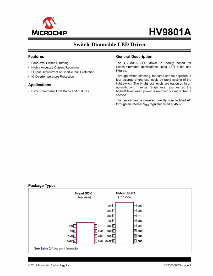
HV9801ASwitch-Dimmable LED Driver
Features
• Four-level Switch Dimming
• Highly Accurate Current Regulator
• Output Overcurrent or Short-circuit Protection
• IC Overtemperature Protection
Applications
• Switch-dimmable LED Bulbs and Fixtures
General Description
The HV9801A LED driver is ideally suited for switch-dimmable applications using LED bulbs and fixtures.
Through switch dimming, the lamp can be adjusted to four discrete brightness levels by rapid cycling of the light switch. The brightness levels are traversed in an up-and-down manner. Brightness resumes at the highest level when power is removed for more than a second.
The device can be powered directly from rectified AC through an internal VDD regulator rated at 450V.
Package Type
See Table 2-1 for pin information.
8-lead SOIC(Top view)
16-lead SOIC(Top view)
1
2
3
4
5
6
7
8
16
15
14
13
12
11
10
9
8
7
6
5
1
2
3
4
VIN
CS
GND
GATE
RT
DNC
VDD
DNC
VIN
DNC
DNC
CS
GND
DNC
DNC
GATE
DNC
DNC
RT
DNC
VDD
DNC
DNC
DNC
s
2017 Microchip Technology Inc. DS20005692A-page 1
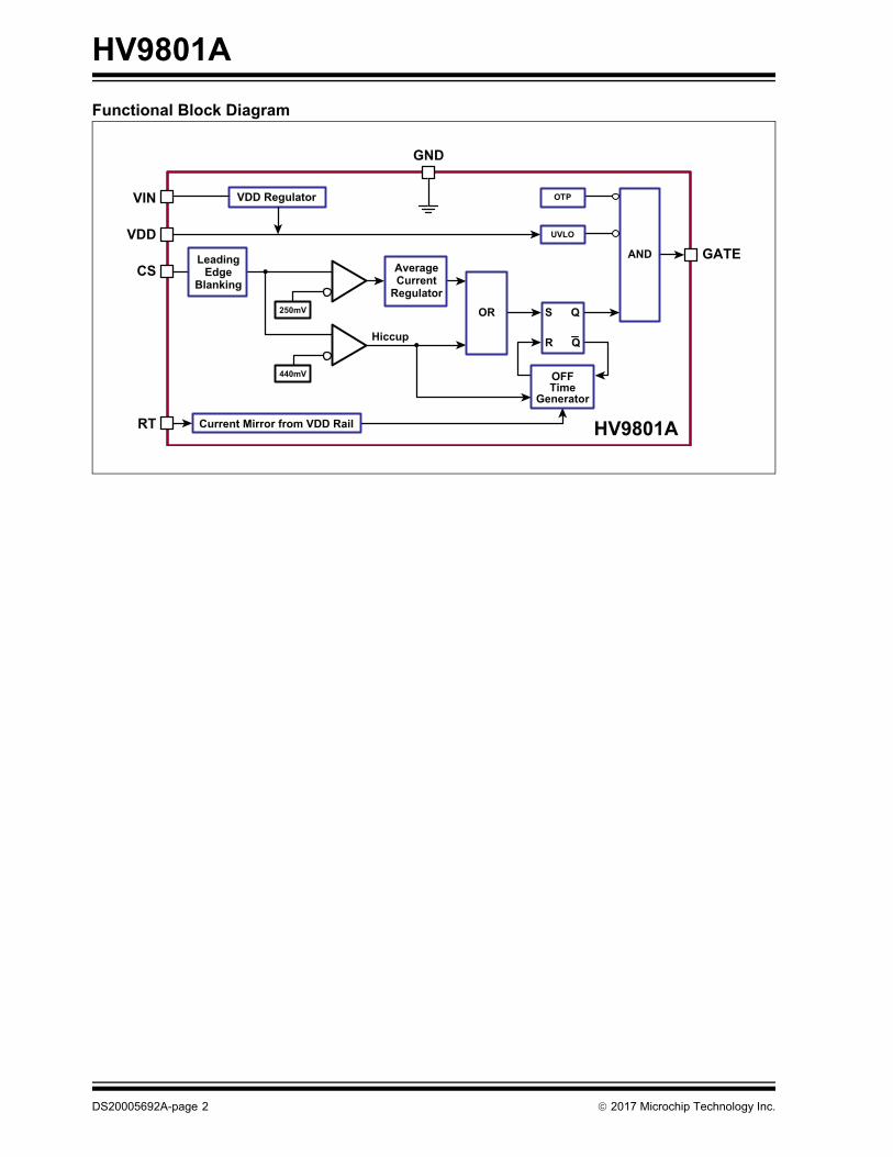
HV9801A
VIN
VDD
CS
RT
GATE
HV9801A
250mV
440mV
VDD Regulator
Current Mirror from VDD Rail
LeadingEdge
Blanking
S Q
R Q
OR
AverageCurrent
Regulator
OFFTime
Generator
OTP
AND
UVLO
GND
Hiccup
Functional Block Diagram
DS20005692A-page 2 2017 Microchip Technology Inc.
HV9801A
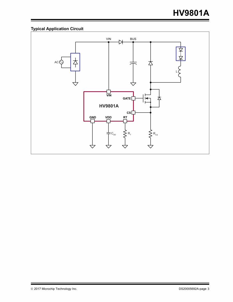
Typical Application Circuit
VINGATE
CSGND VDD RT
HV9801A
CDD RT RCS
L
AC
VIN BUS
2017 Microchip Technology Inc. DS20005692A-page 3
HV9801A
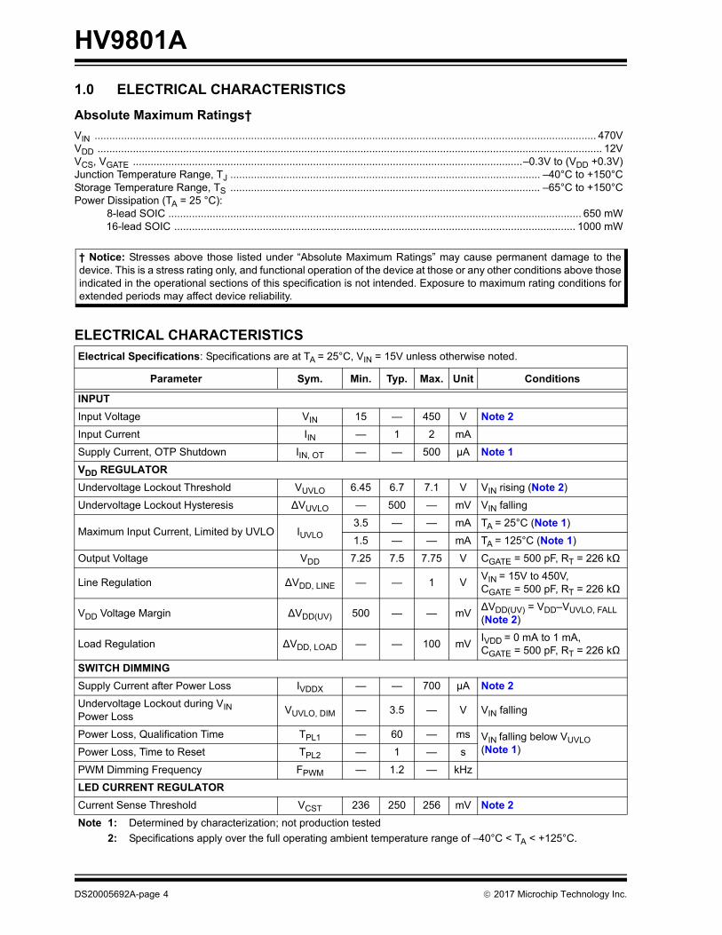
1.0 ELECTRICAL CHARACTERISTICS
Absolute Maximum Ratings†
VIN .......................................................................................................................................................................... 470VVDD ........................................................................................................................................................................... 12VVCS, VGATE ....................................................................................................................................–0.3V to (VDD +0.3V)Junction Temperature Range, TJ ......................................................................................................... –40°C to +150°CStorage Temperature Range, TS ......................................................................................................... –65°C to +150°CPower Dissipation (TA = 25 °C):
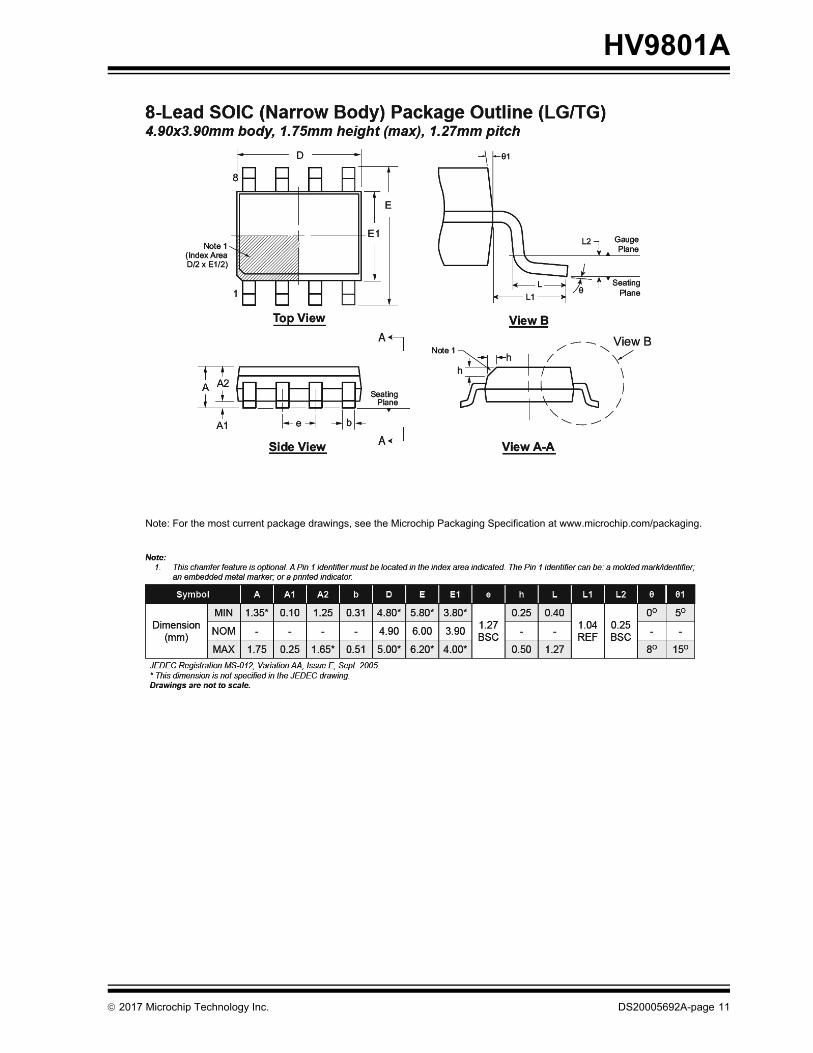
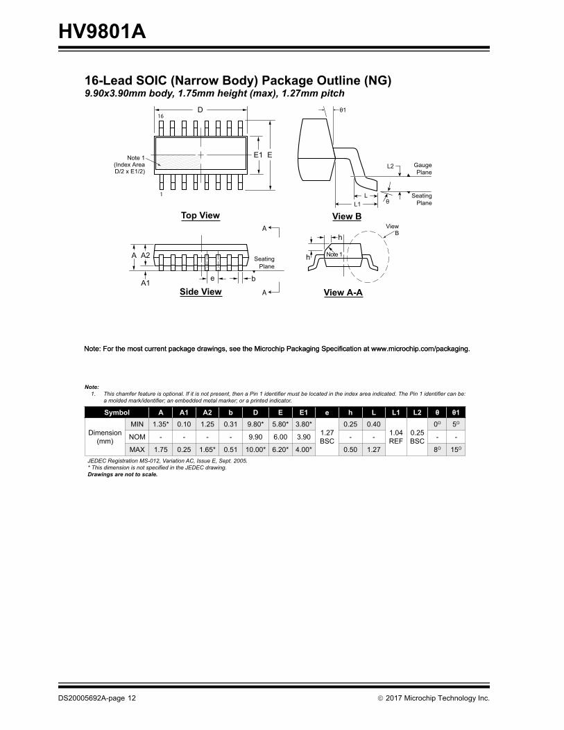
8-lead SOIC ............................................................................................................................................ 650 mW16-lead SOIC ........................................................................................................................................ 1000 mW
† Notice: Stresses above those listed under “Absolute Maximum Ratings” may cause permanent damage to the device. This is a stress rating only, and functional operation of the device at those or any other conditions above those indicated in the operational sections of this specification is not intended. Exposure to maximum rating conditions for extended periods may affect device reliability.
ELECTRICAL CHARACTERISTICS
Electrical Specifications: Specifications are at TA = 25°C, VIN = 15V unless otherwise noted.
Parameter Sym. Min. Typ. Max. Unit Conditions
INPUT
Input Voltage VIN 15 — 450 V Note 2
Input Current IIN — 1 2 mA
Supply Current, OTP Shutdown IIN, OT — — 500 μA Note 1
VDD REGULATOR
Undervoltage Lockout Threshold VUVLO 6.45 6.7 7.1 V VIN rising (Note 2)
Undervoltage Lockout Hysteresis ∆VUVLO — 500 — mV VIN falling
Maximum Input Current, Limited by UVLO IUVLO3.5 — — mA TA = 25°C (Note 1)
1.5 — — mA TA = 125°C (Note 1)
Output Voltage VDD 7.25 7.5 7.75 V CGATE = 500 pF, RT = 226 kΩ
Line Regulation ∆VDD, LINE — — 1 VVIN = 15V to 450V, CGATE = 500 pF, RT = 226 kΩ
VDD Voltage Margin ∆VDD(UV) 500 — — mV∆VDD(UV) = VDD–VUVLO, FALL (Note 2)
Load Regulation ∆VDD, LOAD — — 100 mVIVDD = 0 mA to 1 mA, CGATE = 500 pF, RT = 226 kΩ
SWITCH DIMMING
Supply Current after Power Loss IVDDX — — 700 μA Note 2
Undervoltage Lockout during VIN Power Loss
VUVLO, DIM — 3.5 — V VIN falling
Power Loss, Qualification Time TPL1 — 60 — ms VIN falling below VUVLO (Note 1)Power Loss, Time to Reset TPL2 — 1 — s
PWM Dimming Frequency FPWM — 1.2 — kHz
LED CURRENT REGULATOR
Current Sense Threshold VCST 236 250 256 mV Note 2
Note 1: Determined by characterization; not production tested
2: Specifications apply over the full operating ambient temperature range of –40°C < TA < +125°C.
DS20005692A-page 4 2017 Microchip Technology Inc.

HV9801A
Leading Edge Blanking Time TLEB 110 — 260 ns Note 2
Minimum On-time TONX — — 760 ns VCS = VCST + 30 mV
Maximum Duty Cycle Maintaining Regulation
DMAX 80 — — %LED current falls beyond this duty cycle
SHORT-CIRCUIT PROTECTION
Hiccup Threshold VCSH — 440 — mV
VCS High to Gate Low Delay TDLY — — 180 ns VCS = VCSH + 30 mV
Hiccup Time TSCH — 750 — μs
Minimum On-time TONXSC — — 430 ns VCS = VDD
TOFF TIMER
Off-time TOFF32 40 48
μsRT = 1 MΩ
8 10 12 RT = 226 kΩ
GATE DRIVER
Sourcing Current ISRC 165 — — mA VGATE = 0V
Sinking Current ISINK 165 — — mA VGATE = VDD
Rise Time tr — 30 50 ns CGATE = 500 pF
Fall Time tf — 30 50 ns CGATE = 500 pF
OVERTEMPERATURE PROTECTION
Trip Temperature TTRIP — 140 — °C Note 1
Hysteresis ∆TTRIP — 20 — °C Note 1
TEMPERATURE SPECIFICATIONS
Parameter Sym. Min. Typ. Max. Unit Conditions
TEMPERATURE RANGE
Operating Ambient Temperature TA –40 — +125 °C
Maximum Junction Temperature TJ –40 — +150 °C
Storage Temperature TS –65 — +150 °C
PACKAGE THERMAL RESISTANCE
8-lead SOIC JA — 101 — °C/W
16-lead SOIC JA — 83 — °C/W
ELECTRICAL CHARACTERISTICS (CONTINUED)
Electrical Specifications: Specifications are at TA = 25°C, VIN = 15V unless otherwise noted.
Parameter Sym. Min. Typ. Max. Unit Conditions
Note 1: Determined by characterization; not production tested
2: Specifications apply over the full operating ambient temperature range of –40°C < TA < +125°C.
2017 Microchip Technology Inc. DS20005692A-page 5
HV9801A
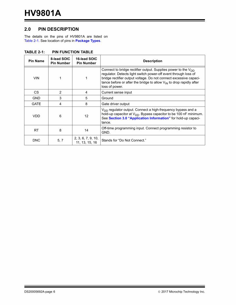
2.0 PIN DESCRIPTION
The details on the pins of HV9801A are listed on Table 2-1. See location of pins in Package Types.
TABLE 2-1: PIN FUNCTION TABLE
Pin Name8-lead SOICPin Number
16-lead SOICPin Number
Description
VIN 1 1
Connect to bridge rectifier output. Supplies power to the VDD regulator. Detects light switch power-off event through loss of bridge rectifier output voltage. Do not connect excessive capaci-tance before or after the bridge to allow VIN to drop rapidly after loss of power.
CS 2 4 Current sense input
GND 3 5 Ground
GATE 4 8 Gate driver output
VDD 6 12
VDD regulator output. Connect a high-frequency bypass and a hold-up capacitor at VDD. Bypass capacitor to be 100 nF minimum. See Section 3.0 “Application Information” for hold-up capaci-tance.
RT 8 14Off-time programming input. Connect programming resistor to GND.
DNC 5, 72, 3, 6, 7, 9, 10, 11, 13, 15, 16
Stands for “Do Not Connect.”
DS20005692A-page 6 2017 Microchip Technology Inc.

HV9801A
3.0 APPLICATION INFORMATION
3.1 Current Control
3.1.1 CONTINUOUS CONDUCTION MODE (CCM)
The HV9801A is designed to control a buck converter operating in CCM.
Continuous Conduction Mode operation is characterized by converter operation with non-zero inductor current throughout the switching cycle. Such operation can be achieved by proper selection of the inductance.
3.1.2 LED CURRENT
The HV9801A regulates the LED current with an accuracy far superior to that of competing Peak Current mode controllers.
Average LED current is set by the current sense resistor RCS and the current regulator reference voltage. See Equation 3-1 and Equation 3-2.
EQUATION 3-1:
V I R=
EQUATION 3-2:
250mV ILED RCS=
For example, a 2Ω resistor corresponds to a 125 mA (average) LED current.
3.1.3 CURRENT CONTROL PERFORMANCE
The control method of the HV9801A virtually eliminates the regulation errors associated with Peak Current mode controllers, such as errors caused by inductor tolerance, propagation delay of the current sense comparator, tolerance in the oscillator frequency or off-timer and changes in line and load voltage.
Figure 3-1 compares the load regulation of the HV9801A and that of a device with peak current control. The graph clearly shows the difference in load regulation between the HV9801A and the HV9910B, which is a peak current regulator.
0.60
0.55
0.50
0.45
0.40
0.35
0.30
0.250 10 20 30 40 50 60
HV9910B
HV9801AVIN = 170VDC
Output Voltage, V
LED
Cur
rent
, A
FIGURE 3-1: Output Characteristics of the HV9801A LED Driver.
3.2 Duty Cycle, Off-time, On-time and Inductor
3.2.1 DUTY CYCLE
The duty cycle (D) is related to the load voltage (VLED) and input voltage (VBUS) by the simple relation shown in Equation 3-3 and Equation 3-4.
EQUATION 3-3:
VOUT D VIN=
EQUATION 3-4:
VLED D VBUS=
3.2.2 OFF-TIME
The HV9801A operates with constant off-time control, which avoids subharmonic oscillation.
Switching period and switching frequency are related to on-time and off-time as shown in Equation 3-5 and Equation 3-6.
EQUATION 3-5:
TSW TON TOFF+=
EQUATION 3-6:
FSW1TSW----------=
2017 Microchip Technology Inc. DS20005692A-page 7
HV9801A
On-time is related to off-time and duty cycle. See Equation 3-7.
EQUATION 3-7:
DTON
TON TOFF+ -----------------------------------=
TON D 1 D– TOFF=
With a given TOFF, the HV9801A dynamically adjusts TON to regulate the LED current. Specifically, TONadapts to the duty cycle associated with the given VBUSand VLED.
3.2.3 OFF-TIME PROGRAMMING
Off-time is programmed by the RT resistor as illustrated in Equation 3-8.
EQUATION 3-8:
TOFF A RT B+=
Where: A = 40 ps / Ω and B = 300 ns
For instance, a 200 kΩ resistor corresponds to 8.3 μs off-time.
An acceptable range for RT is 30 kΩ to 1 MΩ, corresponding to an off-time range between 1.5 µs and 40.3 µs.
3.2.4 INDUCTOR
Because the converter should operate in CCM, the inductor current should not fall to zero within a switching cycle and the inductor current ripple should be sized accordingly.
A common choice for peak-to-peak inductor current ripple (PPR) is 30% to 40% of nominal LED current.
Inductance can be calculated from the current drop during off-time as shown in Equation 3-9 and Equation 3-10.
EQUATION 3-9:
L I V T=
EQUATION 3-10:
L PPR ILED VLED TOFF=
For example, 30% PPR on 350 mA average current equates to 105 mA ripple, which together with 5 µs off-time and 30V LED string voltage corresponds to 1.43 mH inductance.
A design with 30V LED voltage and 150V bus voltage corresponds to a 20% duty cycle, while a 120V bus voltage coincides with a 25% duty cycle. A 20% duty cycle corresponds to 1.25 µs on-time, and a 25% duty
cycle corresponds to 1.67 µs on-time. Hence, the switching frequency is 160 kHz at 150V bus voltage and 150 kHz at 120V bus voltage.
3.2.5 MAXIMUM DUTY CYCLE
Duty cycle should be limited to the specified maximum of 80%. Accordingly, the targeted LED string voltage and the bus voltage are limited to the same ratio. Operation at a larger desired duty cycle than the maximum duty cycle results in an LED current lower than programmed.
3.2.6 MINIMUM DUTY CYCLE
Duty cycle is limited on the low side by the minimum on-time specification (760 ns). Operation at a smaller desired on-time than the minimum causes the LED current to exceed the programmed value.
LED string voltage cannot be made arbitrarily low. Minimum LED string voltage can be determined with Equation 3-11.
EQUATION 3-11:
DMINTONX
TOFF TONX+ --------------------------------------=
VLED DMIN VBUS=
For instance, with 5 µs off-time, the duty cycle should be kept above 13%. Such a duty cycle corresponds to an LED string voltage of 19.5V at 150V bus voltage.
A design that needs a lower LED string voltage requires a longer off-time.
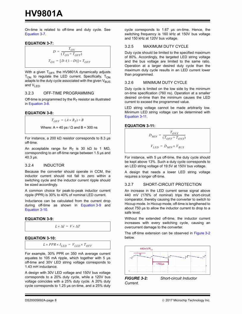
3.2.7 SHORT-CIRCUIT PROTECTION
An increase in the LED current sense signal above 440 mV (176% of nominal) trips the short-circuit comparator, thereby causing the converter to switch to Hiccup mode. In Hiccup mode, off-time is lengthened to about 750 µs to allow the inductor current to drop to a safe level.
Without the extended off-time, the inductor current increases with every switching cycle, causing an overcurrent damage to the converter.
The off-time extension can be observed in Figure 3-2 below.
~750µs
440mV/RCS
S
FIGURE 3-2: Short-circuit Inductor Current.
DS20005692A-page 8 2017 Microchip Technology Inc.
HV9801A
3.2.8 LEADING EDGE BLANKING
The MOSFET drain current and the current sense signal exhibit a spike at the start of a switching cycle, which arises from the MOSFET gate charging current and the current required for discharging the MOSFET drain node. These two currents typically exceed the inductor by quite a margin.
The current sense signal is blanked at the start of the switching cycle in order to avoid a premature trigger of the current sense and the short-circuit protection comparators.
3.2.9 VDD REGULATOR
The VDD regulator generates a source of regulated voltage for operation of internal and external circuits from the power applied at the VIN pin. Alternatively, the VDD voltage can be supplied from a source directly connected to the VDD pin.
3.3 Switch Dimming
3.3.1 GENERAL
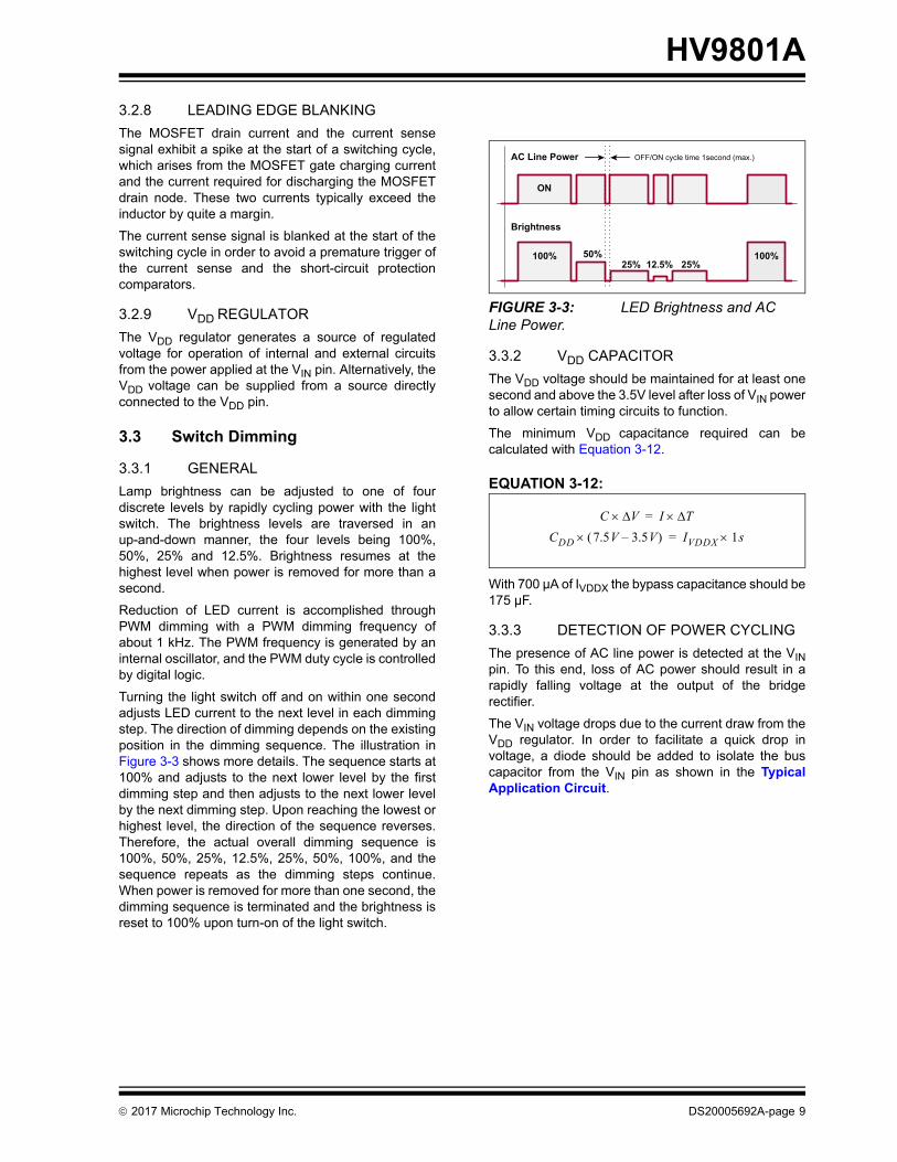
Lamp brightness can be adjusted to one of four discrete levels by rapidly cycling power with the light switch. The brightness levels are traversed in an up-and-down manner, the four levels being 100%, 50%, 25% and 12.5%. Brightness resumes at the highest level when power is removed for more than a second.
Reduction of LED current is accomplished through PWM dimming with a PWM dimming frequency of about 1 kHz. The PWM frequency is generated by an internal oscillator, and the PWM duty cycle is controlled by digital logic.
Turning the light switch off and on within one second adjusts LED current to the next level in each dimming step. The direction of dimming depends on the existing position in the dimming sequence. The illustration in Figure 3-3 shows more details. The sequence starts at 100% and adjusts to the next lower level by the first dimming step and then adjusts to the next lower level by the next dimming step. Upon reaching the lowest or highest level, the direction of the sequence reverses. Therefore, the actual overall dimming sequence is 100%, 50%, 25%, 12.5%, 25%, 50%, 100%, and the sequence repeats as the dimming steps continue. When power is removed for more than one second, the dimming sequence is terminated and the brightness is reset to 100% upon turn-on of the light switch.
OFF/ON cycle time 1second (max.)
100% 50%25% 12.5% 25%
100%
Brightness
AC Line Power
ON
FIGURE 3-3: LED Brightness and AC Line Power.
3.3.2 VDD CAPACITOR
The VDD voltage should be maintained for at least one second and above the 3.5V level after loss of VIN power to allow certain timing circuits to function.
The minimum VDD capacitance required can be calculated with Equation 3-12.
EQUATION 3-12:
C V I T=
CDD 7.5V 3.5V– IVDDX 1s=
With 700 µA of IVDDX the bypass capacitance should be 175 µF.
3.3.3 DETECTION OF POWER CYCLING
The presence of AC line power is detected at the VINpin. To this end, loss of AC power should result in a rapidly falling voltage at the output of the bridge rectifier.
The VIN voltage drops due to the current draw from the VDD regulator. In order to facilitate a quick drop in voltage, a diode should be added to isolate the bus capacitor from the VIN pin as shown in the Typical Application Circuit.
2017 Microchip Technology Inc. DS20005692A-page 9
HV9801A
4.0 PACKAGING INFORMATION
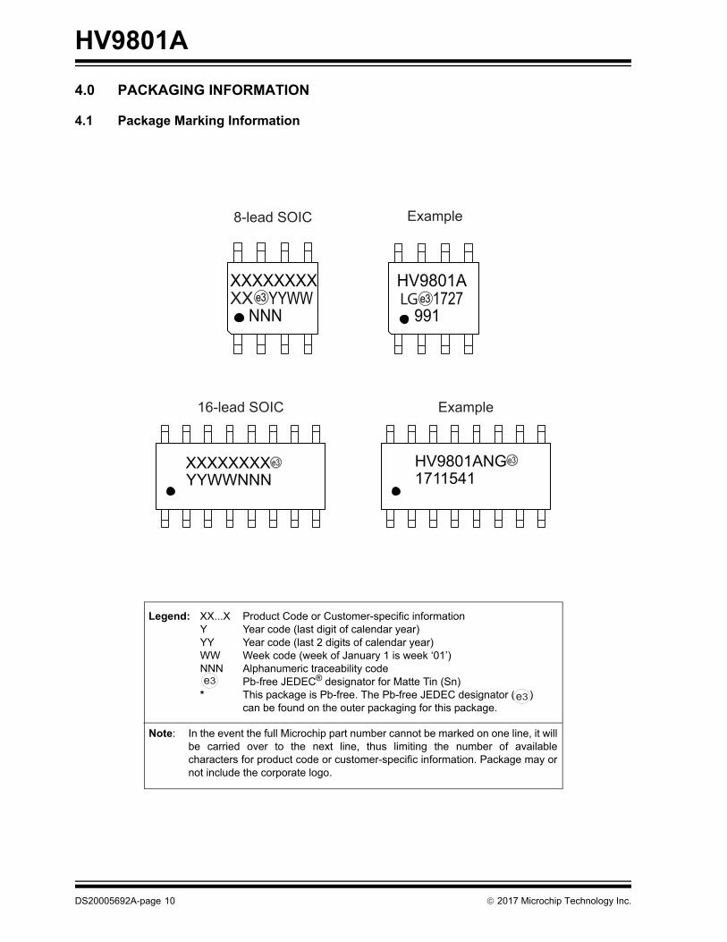
4.1 Package Marking Information
Legend: XX...X Product Code or Customer-specific informationY Year code (last digit of calendar year)YY Year code (last 2 digits of calendar year)WW Week code (week of January 1 is week ‘01’)NNN Alphanumeric traceability code Pb-free JEDEC® designator for Matte Tin (Sn)* This package is Pb-free. The Pb-free JEDEC designator ( )
can be found on the outer packaging for this package.
Note: In the event the full Microchip part number cannot be marked on one line, it will be carried over to the next line, thus limiting the number of available characters for product code or customer-specific information. Package may or not include the corporate logo.
3e
3e
8-lead SOIC Example
NNN
XXXXXXXXYYWWe3
991
HV9801A1727LGXX e3
16-lead SOIC
XXXXXXXXYYWWNNN
e3
Example
HV9801ANG1711541
e3
DS20005692A-page 10 2017 Microchip Technology Inc.
HV9801A
Note: For the most current package drawings, see the Microchip Packaging Specification at www.microchip.com/packaging.
2017 Microchip Technology Inc. DS20005692A-page 11
HV9801A
16-Lead SOIC (Narrow Body) Package Outline (NG)9.90x3.90mm body, 1.75mm height (max), 1.27mm pitch
Symbol A A1 A2 b D E E1 e h L L1 L2
Dimension(mm)
MIN 1.35* 0.10 1.25 0.31 9.80* 5.80* 3.80*1.27BSC
0.25 0.401.04REF
0.25BSC
0O 5O
NOM - - - - 9.90 6.00 3.90 - - - -
MAX 1.75 0.25 1.65* 0.51 10.00* 6.20* 4.00* 0.50 1.27 8O 15O
JEDEC Registration MS-012, Variation AC, Issue E, Sept. 2005.
Drawings are not to scale.
D
SeatingPlane
GaugePlane
LL1
L2
Top View
Side View View A-A
View BView
B
θ1
θ
E1 E
A A2
A1
A
A
SeatingPlane
e b
h
h
16
1
Note 1
Note 1(Index AreaD/2 x E1/2)
Note:1.
Note: For the most current package drawings, see the Microchip Packaging Specification at www.microchip.com/packaging.Note: For the most current package drawings, see the Microchip Packaging Specification at www.microchip.com/packaging.
DS20005692A-page 12 2017 Microchip Technology Inc.
2017 Microchip Technology Inc. DS20005692A-page 13
HV9801A
APPENDIX A: REVISION HISTORY
Revision A (September 2017)
• Converted Supertex Doc# DSFP-HV9801A to Microchip DS20005692A
• Updated the part marking format
• Removed the 16-lead SOIC Narrow (NG) M934 media type
• Changed the quantity of the 8-lead SOIC (Nar-row) LG package from 2500/Reel to 3300/Reel
• Made minor text changes throughout the document

HV9801A
DS20005692A-page 14 2017 Microchip Technology Inc.
PRODUCT IDENTIFICATION SYSTEM
To order or obtain information, e.g., on pricing or delivery, contact your local Microchip representative or sales office.
Examples:
a) HV9801ALG-G: Switch-Dimmable LED Driver, 8-lead SOIC Package, 3300/Reel
b) HV9801ANG-G: Switch-Dimmable LED Driver, 16-lead SOIC Package, 45/Tube
PART NO.
Device
Device: HV9801A = Switch-Dimmable LED Driver
Packages: LG = 8-lead SOIC
NG = 16-lead SOIC
Environmental: G = Lead (Pb)-free/RoHS-compliant Package
Media Type: (blank) = 3300/Reel for an LG Package
= 45/Tube for an NG Package
XX
Package
- X - X
Environmental Media Type Options
Note the following details of the code protection feature on Microchip devices:
• Microchip products meet the specification contained in their particular Microchip Data Sheet.
• Microchip believes that its family of products is one of the most secure families of its kind on the market today, when used in the intended manner and under normal conditions.
• There are dishonest and possibly illegal methods used to breach the code protection feature. All of these methods, to our knowledge, require using the Microchip products in a manner outside the operating specifications contained in Microchip’s Data Sheets. Most likely, the person doing so is engaged in theft of intellectual property.
• Microchip is willing to work with the customer who is concerned about the integrity of their code.
• Neither Microchip nor any other semiconductor manufacturer can guarantee the security of their code. Code protection does not mean that we are guaranteeing the product as “unbreakable.”
Code protection is constantly evolving. We at Microchip are committed to continuously improving the code protection features of our products. Attempts to break Microchip’s code protection feature may be a violation of the Digital Millennium Copyright Act. If such acts allow unauthorized access to your software or other copyrighted work, you may have a right to sue for relief under that Act.
Information contained in this publication regarding device applications and the like is provided only for your convenience and may be superseded by updates. It is your responsibility to ensure that your application meets with your specifications. MICROCHIP MAKES NO REPRESENTATIONS OR WARRANTIES OF ANY KIND WHETHER EXPRESS OR IMPLIED, WRITTEN OR ORAL, STATUTORY OR OTHERWISE, RELATED TO THE INFORMATION, INCLUDING BUT NOT LIMITED TO ITS CONDITION, QUALITY, PERFORMANCE, MERCHANTABILITY OR FITNESS FOR PURPOSE. Microchip disclaims all liability arising from this information and its use. Use of Microchip devices in life support and/or safety applications is entirely at the buyer’s risk, and the buyer agrees to defend, indemnify and hold harmless Microchip from any and all damages, claims, suits, or expenses resulting from such use. No licenses are conveyed, implicitly or otherwise, under any Microchip intellectual property rights unless otherwise stated.
2017 Microchip Technology Inc.
Microchip received ISO/TS-16949:2009 certification for its worldwide headquarters, design and wafer fabrication facilities in Chandler and Tempe, Arizona; Gresham, Oregon and design centers in California and India. The Company’s quality system processes and procedures are for its PIC® MCUs and dsPIC® DSCs, KEELOQ® code hopping devices, Serial EEPROMs, microperipherals, nonvolatile memory and analog products. In addition, Microchip’s quality system for the design and manufacture of development systems is ISO 9001:2000 certified.
QUALITYMANAGEMENTSYSTEMCERTIFIEDBYDNV
== ISO/TS16949==
Trademarks
The Microchip name and logo, the Microchip logo, AnyRate, AVR, AVR logo, AVR Freaks, BeaconThings, BitCloud, CryptoMemory, CryptoRF, dsPIC, FlashFlex, flexPWR, Heldo, JukeBlox, KEELOQ, KEELOQ logo, Kleer, LANCheck, LINK MD, maXStylus, maXTouch, MediaLB, megaAVR, MOST, MOST logo, MPLAB, OptoLyzer, PIC, picoPower, PICSTART, PIC32 logo, Prochip Designer, QTouch, RightTouch, SAM-BA, SpyNIC, SST, SST Logo, SuperFlash, tinyAVR, UNI/O, and XMEGA are registered trademarks of Microchip Technology Incorporated in the U.S.A. and other countries.
ClockWorks, The Embedded Control Solutions Company, EtherSynch, Hyper Speed Control, HyperLight Load, IntelliMOS, mTouch, Precision Edge, and Quiet-Wire are registered trademarks of Microchip Technology Incorporated in the U.S.A.
Adjacent Key Suppression, AKS, Analog-for-the-Digital Age, Any Capacitor, AnyIn, AnyOut, BodyCom, chipKIT, chipKIT logo, CodeGuard, CryptoAuthentication, CryptoCompanion, CryptoController, dsPICDEM, dsPICDEM.net, Dynamic Average Matching, DAM, ECAN, EtherGREEN, In-Circuit Serial Programming, ICSP, Inter-Chip Connectivity, JitterBlocker, KleerNet, KleerNet logo, Mindi, MiWi, motorBench, MPASM, MPF, MPLAB Certified logo, MPLIB, MPLINK, MultiTRAK, NetDetach, Omniscient Code Generation, PICDEM, PICDEM.net, PICkit, PICtail, PureSilicon, QMatrix, RightTouch logo, REAL ICE, Ripple Blocker, SAM-ICE, Serial Quad I/O, SMART-I.S., SQI, SuperSwitcher, SuperSwitcher II, Total Endurance, TSHARC, USBCheck, VariSense, ViewSpan, WiperLock, Wireless DNA, and ZENA are trademarks of Microchip Technology Incorporated in the U.S.A. and other countries.
SQTP is a service mark of Microchip Technology Incorporated in the U.S.A.
Silicon Storage Technology is a registered trademark of Microchip Technology Inc. in other countries.
GestIC is a registered trademark of Microchip Technology Germany II GmbH & Co. KG, a subsidiary of Microchip Technology Inc., in other countries.
All other trademarks mentioned herein are property of their respective companies.
© 2017, Microchip Technology Incorporated, All Rights Reserved.
ISBN: 978-1-5224-2134-4
DS20005692A-page 15

DS20005692A-page 16 2017 Microchip Technology Inc.
AMERICASCorporate Office2355 West Chandler Blvd.Chandler, AZ 85224-6199Tel: 480-792-7200 Fax: 480-792-7277Technical Support: http://www.microchip.com/supportWeb Address: www.microchip.com
AtlantaDuluth, GA Tel: 678-957-9614 Fax: 678-957-1455
Austin, TXTel: 512-257-3370
BostonWestborough, MA Tel: 774-760-0087 Fax: 774-760-0088
ChicagoItasca, IL Tel: 630-285-0071 Fax: 630-285-0075
DallasAddison, TX Tel: 972-818-7423 Fax: 972-818-2924
DetroitNovi, MI Tel: 248-848-4000
Houston, TX Tel: 281-894-5983
IndianapolisNoblesville, IN Tel: 317-773-8323Fax: 317-773-5453Tel: 317-536-2380
Los AngelesMission Viejo, CA Tel: 949-462-9523Fax: 949-462-9608Tel: 951-273-7800
Raleigh, NC Tel: 919-844-7510
New York, NY Tel: 631-435-6000
San Jose, CA Tel: 408-735-9110Tel: 408-436-4270
Canada - TorontoTel: 905-695-1980 Fax: 905-695-2078
ASIA/PACIFICAsia Pacific OfficeSuites 3707-14, 37th FloorTower 6, The GatewayHarbour City, Kowloon
Hong KongTel: 852-2943-5100Fax: 852-2401-3431
Australia - SydneyTel: 61-2-9868-6733Fax: 61-2-9868-6755
China - BeijingTel: 86-10-8569-7000 Fax: 86-10-8528-2104
China - ChengduTel: 86-28-8665-5511Fax: 86-28-8665-7889
China - ChongqingTel: 86-23-8980-9588Fax: 86-23-8980-9500
China - DongguanTel: 86-769-8702-9880
China - GuangzhouTel: 86-20-8755-8029
China - HangzhouTel: 86-571-8792-8115 Fax: 86-571-8792-8116
China - Hong Kong SARTel: 852-2943-5100 Fax: 852-2401-3431
China - NanjingTel: 86-25-8473-2460Fax: 86-25-8473-2470
China - QingdaoTel: 86-532-8502-7355Fax: 86-532-8502-7205
China - ShanghaiTel: 86-21-3326-8000 Fax: 86-21-3326-8021
China - ShenyangTel: 86-24-2334-2829Fax: 86-24-2334-2393
China - ShenzhenTel: 86-755-8864-2200 Fax: 86-755-8203-1760
China - WuhanTel: 86-27-5980-5300Fax: 86-27-5980-5118
China - XianTel: 86-29-8833-7252Fax: 86-29-8833-7256
ASIA/PACIFICChina - XiamenTel: 86-592-2388138 Fax: 86-592-2388130
China - ZhuhaiTel: 86-756-3210040 Fax: 86-756-3210049
India - BangaloreTel: 91-80-3090-4444 Fax: 91-80-3090-4123
India - New DelhiTel: 91-11-4160-8631Fax: 91-11-4160-8632
India - PuneTel: 91-20-3019-1500
Japan - OsakaTel: 81-6-6152-7160 Fax: 81-6-6152-9310
Japan - TokyoTel: 81-3-6880- 3770 Fax: 81-3-6880-3771
Korea - DaeguTel: 82-53-744-4301Fax: 82-53-744-4302
Korea - SeoulTel: 82-2-554-7200Fax: 82-2-558-5932 or 82-2-558-5934
Malaysia - Kuala LumpurTel: 60-3-6201-9857Fax: 60-3-6201-9859
Malaysia - PenangTel: 60-4-227-8870Fax: 60-4-227-4068
Philippines - ManilaTel: 63-2-634-9065Fax: 63-2-634-9069
SingaporeTel: 65-6334-8870Fax: 65-6334-8850
Taiwan - Hsin ChuTel: 886-3-5778-366Fax: 886-3-5770-955
Taiwan - KaohsiungTel: 886-7-213-7830
Taiwan - TaipeiTel: 886-2-2508-8600 Fax: 886-2-2508-0102
Thailand - BangkokTel: 66-2-694-1351Fax: 66-2-694-1350
EUROPEAustria - WelsTel: 43-7242-2244-39Fax: 43-7242-2244-393
Denmark - CopenhagenTel: 45-4450-2828 Fax: 45-4485-2829
Finland - EspooTel: 358-9-4520-820
France - ParisTel: 33-1-69-53-63-20 Fax: 33-1-69-30-90-79
France - Saint CloudTel: 33-1-30-60-70-00
Germany - GarchingTel: 49-8931-9700Germany - HaanTel: 49-2129-3766400
Germany - HeilbronnTel: 49-7131-67-3636
Germany - KarlsruheTel: 49-721-625370
Germany - MunichTel: 49-89-627-144-0 Fax: 49-89-627-144-44
Germany - RosenheimTel: 49-8031-354-560
Israel - Ra’anana Tel: 972-9-744-7705
Italy - Milan Tel: 39-0331-742611 Fax: 39-0331-466781
Italy - PadovaTel: 39-049-7625286
Netherlands - DrunenTel: 31-416-690399 Fax: 31-416-690340
Norway - TrondheimTel: 47-7289-7561
Poland - WarsawTel: 48-22-3325737
Romania - BucharestTel: 40-21-407-87-50
Spain - MadridTel: 34-91-708-08-90Fax: 34-91-708-08-91
Sweden - GothenbergTel: 46-31-704-60-40
Sweden - StockholmTel: 46-8-5090-4654
UK - WokinghamTel: 44-118-921-5800Fax: 44-118-921-5820
Worldwide Sales and Service
11/07/16