CESDig & CEletro 2018/19 / Elect. Fundamentals Floyd & Buchla © Pearson Education. © Trustees of Boston University 03-12-2018
Circuitos Elétricos e Sistemas Digitais2018-2019 - 1.º Semestre
Técnicas sistemáticas de análise de circuitos
• Método das malhas e dos nós para análise de circuitos– Nó, ramo, malha – Elemento, característica i-v do elemento – Leis de Kirchhoff dos nós e das malhas
• Etapas da aplicação do método das malhas e dos nós
• Exemplos de circuitos resistivos
• Introdução a Ferramentas de Projeto (CAD): O Simulador SPICE
1CESDig 2018/2019 03-12-2018

CESDig & CEletro 2018/19 / Elect. Fundamentals Floyd & Buchla © Pearson Education. © Trustees of Boston University 03-12-2018
Métodos das malhas e dos nós para análise de circuitos
Node & Mesh Method of Circuit Analysis
2

CESDig & CEletro 2018/19 / Elect. Fundamentals Floyd & Buchla © Pearson Education. © Trustees of Boston University 03-12-2018
Kirchhoff’s Voltage Law (KVL): “A somas das tensões ao longo de uma malha é igual a zero.”(Ter em atenção a polaridade das tensões.) Exemplos:
v1 + v2 + v3 = 0
+v1–
–v2+
+– v3
v1 - v2 + v3 = 0
+v1–
+v2-
+– v3
Leis de Kirchhoff das malhas e dos nós
3
Kirchhoff’s Current Law (KCL): “A somas das corrente que entram num nó é igual a zero.” (Ter em atenção os sentidos das correntes. Consideram-se positivas as correntes que entram no nó.) Exemplos:
i1 i2
i3 i1 + i2 + i3 = 0
i1 i2
i3 i1 - i2 + i3 = 0
Sentido de circulação na malha

CESDig & CEletro 2018/19 / Elect. Fundamentals Floyd & Buchla © Pearson Education. © Trustees of Boston University 03-12-2018
Equação características tensão-corrente (V-I)
4
Caraterística tensão corrente (V-I) [Voltage-Current (V-I) Characteristic] de um
elemento do circuito: equação que relaciona a tensão aos terminais do componente
com a corrente que o atravessa: v = f(i)
v = i R
i+ v –
Exemplos: característica V-I para uma resistência (Lei de Ohm)
+_+
v
–
i
v = - i R
i- v +
Fonte de tensão independente
v =constante+
v
–i
i =constante
Fonte de corrente independente
A corrente é determinada pelo circuito
A tensão é determinada pelo circuito

CESDig & CEletro 2018/19 / Elect. Fundamentals Floyd & Buchla © Pearson Education. © Trustees of Boston University 03-12-2018
Métodos de análise de circuitos
5
Os circuitos que vimos “até agora” não são muito difíceis de analisar usando as leis dos circuitos (lei de Ohm, leis de Kirchhoff, etc.) e as técnicas de simplificação de circuitos (associação de componentes em série e paralelo). Contudo, na vida real deparámo-nos, por vezes, com circuito complexos em que é mais difícil apontar o procedimento de análise mais expedito. Torna-se pois necessário ter um procedimento de análise que pode ser aplicado de forma quase mecânica. A técnica de exame de um circuito mais comum é a análise nodal (método dos nós). Considere-se o circuito da figura ao lado. Uma forma simples de ficarmos a conhecer quantas tensões diferentes devemos determinar na análise a efetuar, é remover os componentes e deixar as conexões, figura seguinte. As zonas sombreadas indicam regiões de tensão constante, e são conhecidas como nós. Neste caso podemos concluir que o circuito tem 4 nós.Se ligarmos uma das pontas de prova de um voltímetro a um destes nós, há três valores diferentes de tensão no circuito que podem ser medidos com a outra prova. É por isso conveniente definir um nó a partir do qual se medem todas as tensões no circuito (nó terra /comum). Este é o primeiro de 4 passos de uma metodologias de análise sistemática. O segundo passo consiste em nomear os restantes nós (neste caso A, B e C), e identificar as respetivas tensões VA, VB, e VC.
O terceiro passo consiste em aplicar a lei de Kirchhoff da corrente em cada nó, substituindo cada uma das correntes nessas equações pelas expressões que resultam da lei de Ohm, obtendo-se assim as equações das tensões nodais. O quarto passo consiste em resolver as equações.

CESDig & CEletro 2018/19 / Elect. Fundamentals Floyd & Buchla © Pearson Education. © Trustees of Boston University 03-12-2018
Métodos de análise de circuitos
6
Lei dos nós (“A somas das correntes entrando num nó é nula”) aplicada o nó A (unidades A, V, Ω):
Lei dos nós aplicada o nó B (mA, V, kΩ):
Em mA, V, kΩ:
Lei dos nós aplicada o nó C (mA, V, kΩ):
Seja o circuito da Figura.
Estas três equações formam o sistema de equações das tensões nodais. Temos tantas equações quantas as tensões desconhecidas (incógnitas). Estas equação são lineares na tensão e podem ser resolvidas de forma convencional (por exemplo, eliminação sucessiva) ou por um método numérico apropriado. Por forma a facilitar o processo de resolução é conveniente reescrever as equações na forma:
Obtendo-se:
A partir destes valores obtém-se todas as tensões e correntes.

CESDig & CEletro 2018/19 / Elect. Fundamentals Floyd & Buchla © Pearson Education. © Trustees of Boston University 03-12-2018 7
Basic engineering circuit analysis 11E irwin

CESDig & CEletro 2018/19 / Elect. Fundamentals Floyd & Buchla © Pearson Education. © Trustees of Boston University 03-12-2018
Exemplo de aplicação do método dos nós
8
CESDig & CEletro 2018/19 / Elect. Fundamentals Floyd & Buchla © Pearson Education. © Trustees of Boston University 03-12-2018 9
Basic engineering circuit analysis 11E irwin

CESDig & CEletro 2018/19 / Elect. Fundamentals Floyd & Buchla © Pearson Education. © Trustees of Boston University 03-12-2018
Exemplo de aplicação método das malhas
10

CESDig & CEletro 2018/19 / Elect. Fundamentals Floyd & Buchla © Pearson Education. © Trustees of Boston University 03-12-2018
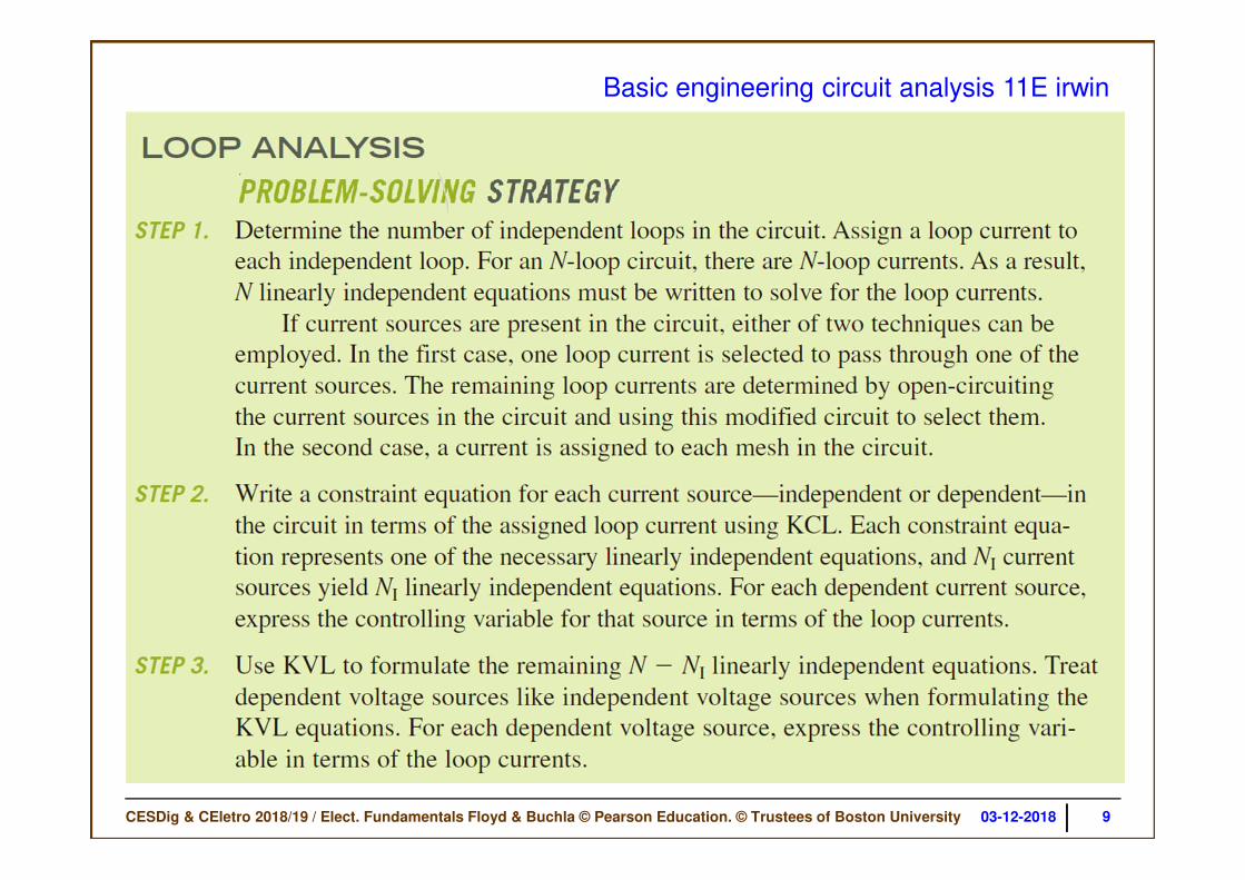
Análise de circuitos usando o método das malhas e dos nós
Passos para a aplicação do método:
• Escolher o nó comum/terra e numerar/identificar os restantes nós
• Escrever a lei de Kirchhoff das corrente (KCL) para cada nó do circuito, excluindo
o nó designado como comum.
• Escrever a lei de Kirchhoff das malhas (KVL) para cada malha do circuito.
• Escrever as equações características tensão-corrente (V-I) para cada elemento
no circuito, e fazer a respetiva substituição nas equações anteriores.
• Resolver o conjunto de equações em ordem às tensões e às correntes.
11
malha
Sentido de circulação na malha
O método dos nós/malhas é um procedimento formal de usar as lei de Kirchhoffdos nós (KCL) e das malhas (KVL).

CESDig & CEletro 2018/19 / Elect. Fundamentals Floyd & Buchla © Pearson Education. © Trustees of Boston University 03-12-2018
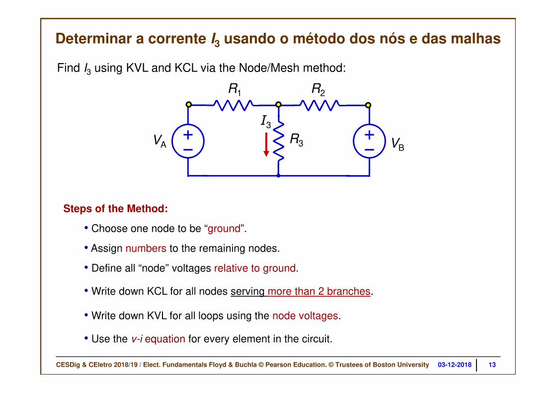
Find I3 in the following circuit:
VA VB
R1 R2
R3
I3
• The circuit is driven by two sources, VA and VB .
• Both sources contribute to I3 .
Q: How can we find the current I3 ?
What do we know?
• The circuit contains only sources and resistors.
A: One way: Solve for I3 using the node & mesh method
Resistive Circuit
Exemplo de aplicação: Determinar a corrente I3
12
CESDig & CEletro 2018/19 / Elect. Fundamentals Floyd & Buchla © Pearson Education. © Trustees of Boston University 03-12-2018
Find I3 using KVL and KCL via the Node/Mesh method:
• Write down KVL for all loops using the node voltages.
• Choose one node to be “ground”.
VA VB
R1 R2
R3
I3
• Define all “node” voltages relative to ground.
• Write down KCL for all nodes serving more than 2 branches.
Steps of the Method:
• Use the v-i equation for every element in the circuit.
• Assign numbers to the remaining nodes.
Determinar a corrente I3 usando o método dos nós e das malhas
13
CESDig & CEletro 2018/19 / Elect. Fundamentals Floyd & Buchla © Pearson Education. © Trustees of Boston University 03-12-2018
VA VB
1 2 3
I1 I
2
BA
• Assign numbers to the remaining nodes.
• Choose one node to be “ground”.
• Define all “node” voltages relative to ground.
+v1
–
+v3
–
• Voltages between two nodes defined as their difference:
v12 = v1 – v21 2
R1
+ v12 –
+ v12 –
I3
Escolher o nó comum/terra, numerar os restantes nós, e definir a tensão em cada nó
14
R1 +v2
–
R2
- v23 +
R3

CESDig & CEletro 2018/19 / Elect. Fundamentals Floyd & Buchla © Pearson Education. © Trustees of Boston University 03-12-2018
• Write down KCL for node 2:
VA VB
R1 R2
I3
1 2 3
I1 I2
BA
I1 + I2 − I3 = 0
• Write down KCL for all nodes serving more than 2 branches.
Escrever a equação dos nós para cada nó
15
R3
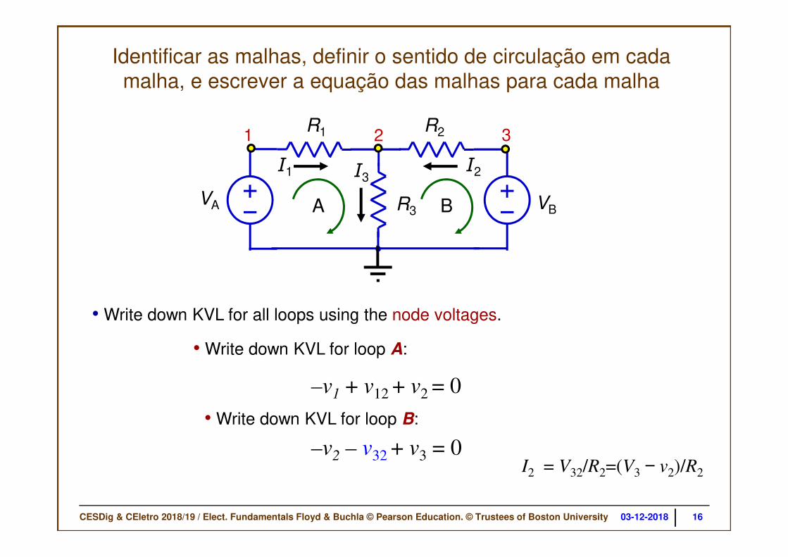
CESDig & CEletro 2018/19 / Elect. Fundamentals Floyd & Buchla © Pearson Education. © Trustees of Boston University 03-12-2018
VA VB
R1 R2
R3
I3
1 2 3
I1 I2
BA
• Write down KVL for loop A:
–v1
+ v12 + v2 = 0
• Write down KVL for loop B:
• Write down KVL for all loops using the node voltages.
–v2
– v32 + v3 = 0
Identificar as malhas, definir o sentido de circulação em cada malha, e escrever a equação das malhas para cada malha
16
I2 = V32/R2=(V3 − v2)/R2

CESDig & CEletro 2018/19 / Elect. Fundamentals Floyd & Buchla © Pearson Education. © Trustees of Boston University 03-12-2018
VA VB
R1 R2
R3
I3
1 2 3
I1 I2
BA
From Ohm’s Law:
I1 = (VA
− v2)/R1
I2 = (VB
− v2)/R2
I3 = v2/R3
• Use the v-i equation for every element in the circuit.
By Inspection:
v1 = VA
v3 = VB
Escrever as equações i-v para cada elemento
17
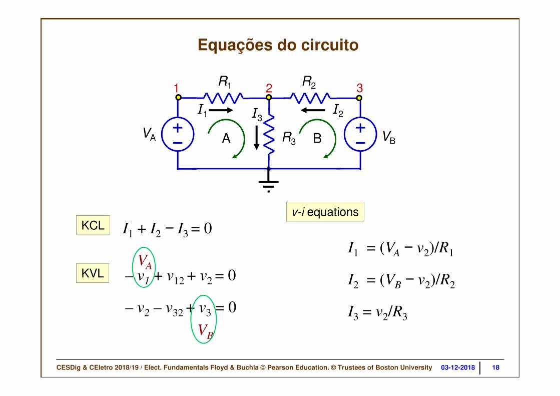
CESDig & CEletro 2018/19 / Elect. Fundamentals Floyd & Buchla © Pearson Education. © Trustees of Boston University 03-12-2018
VA VB
R1 R2
R3
I3
1 2 3
I1 I2
BA
I1 + I2 − I3 = 0KCL
I1 = (VA
− v2)/R1
I2 = (VB
− v2)/R2
I3 = v2/R3
v-i equations
KVL – v1
+ v12 + v2 = 0
– v2
– v32 + v3 = 0
VA
VB
Equações do circuito
18
CESDig & CEletro 2018/19 / Elect. Fundamentals Floyd & Buchla © Pearson Education. © Trustees of Boston University 03-12-2018
I1 = (VA
− v2)/R1
I2 = (VB
− v2)/R2
I3 = v2/R3
v-i equations
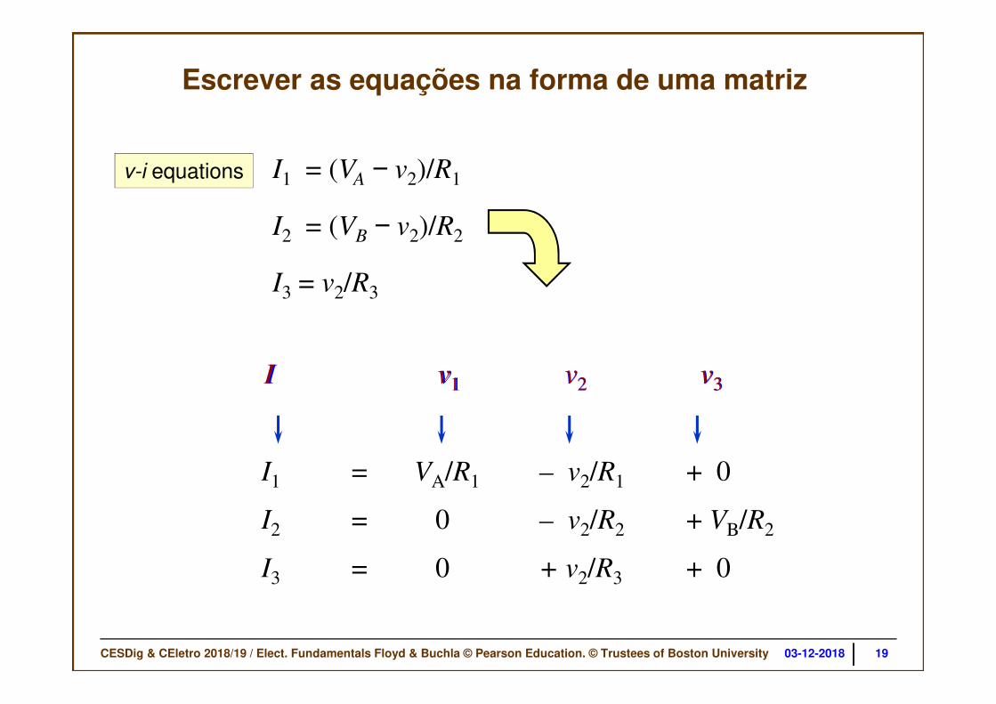
I v1 v2 v3
I1 = VA/R1 – v2/R1 + 0
I2 = 0 – v2/R2 + VB/R2
I3 = 0 + v2/R3 + 0
Escrever as equações na forma de uma matriz
I v1 v2 v3
19

CESDig & CEletro 2018/19 / Elect. Fundamentals Floyd & Buchla © Pearson Education. © Trustees of Boston University 03-12-2018
I v1 v2 v3
I1 = VA/R1 – v2/R1 + 0
I2 = 0 – v2/R2 + VB/R2
I3 = 0 + v2/R3 + 0
I v1 v2 v3
I1 + I2 − I3 = 0KCL
= 0VA/R1 – v2/R1 – v2/R2 + VB/R2 – v2/R3
1
R1
1
R2
1
R3+ +v2
VA
R1
VB
R2
+ =
Determinação de v2
20
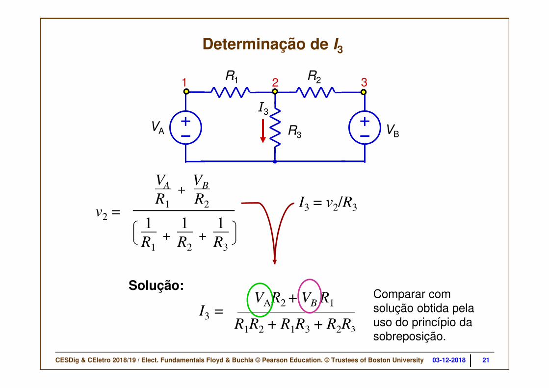
CESDig & CEletro 2018/19 / Elect. Fundamentals Floyd & Buchla © Pearson Education. © Trustees of Boston University 03-12-2018
Solução:VAR2 + V
B R1
I3 = R1R2 + R1R3 + R2R3
VA VB
R1 R2
R3
I3
1 2 3
v2 =1
R1
1
R2
1
R3+ +
VA
R1
VB
R2
+I3 = v2/R3
21
Determinação de I3
Comparar com solução obtida pela uso do princípio da sobreposição.
CESDig & CEletro 2018/19 / Elect. Fundamentals Floyd & Buchla © Pearson Education. © Trustees of Boston University 03-12-2018
Ferramentas de simulação e análise de circuitos elétricos
O Simulador PSPICE
(ver guia do trabalho n.º 3)
22
http://webpages.ciencias.ulisboa.pt/%7Ejmfigueiredo/aulas/CEeSD_CE_201819.htm#Guiasp

CESDig & CEletro 2018/19 / Elect. Fundamentals Floyd & Buchla © Pearson Education. © Trustees of Boston University 03-12-2018
PSpice e MultiSim
23
SPICE (acrónimo de Simulated Program with Integrated Circuits Emphasis, ou Programa de Simulação com ênfase em Circuitos Integrados) é um software de simulação de circuitos analógicos. É uma poderosa ferramenta usada para testar, e antever comportamento de circuitos contendo circuitos integrados, resistências, bobines, transístores, condensadores, díodos e outros componentes elétricos e eletrónicos. Versões comerciais: PSpice/OrCAD, HSpice (para UNIX), HSIM, MicroCad, NG-spice, MultiSIM, SmartSpice, TINA, MacSpice, NanoSim, NSPICE, LTSpice, ….
Electronics Workbench Inc. é uma subsidiária da National Instruments e desenvolve o MultiSIM, um programa de simulação e análise de circuitos elétricos. O programa chamava-se anteriormente Electronics Workbench.
O OrCAD representa pacote de software proprietário usado na simulação e projeto de circuitos eletrónicos, principalmente no desenho de placas de circuitos impressos. O nome OrCAD reflete a origem do software: Oregon + CAD. A linha de produtos OrCAD é propriedade da Cadence Design Systems.
Ver: PSpice 9.1 student version + guia_versão_0.1
(http://webpages.ciencias.ulisboa.pt/~jmfigueiredo/aulas/CEeSD_CE_201819.htm#Guiasp)

CESDig & CEletro 2018/19 / Elect. Fundamentals Floyd & Buchla © Pearson Education. © Trustees of Boston University 03-12-2018
Circuitos Elétricos e Sistemas Digitais2018-2019 - 1.º Semestre
Exemplos de circuitos resistivos práticos
• Exemplos de circuitos resistivos e aplicações
• Fonte alimentando várias cargas simultaneamente
• Potencia fornecida a vários altifalantes
• Atenuador resistivo
• Amplificadores com transístores
• Circuitos com potenciómetros
• Redes R-2R para conversores digitais-analógicos (Digital-to-Analog
Converter (R-2R Ladder)
24CESDig 2018/2019 03-12-2018

CESDig & CEletro 2018/19 / Elect. Fundamentals Floyd & Buchla © Pearson Education. © Trustees of Boston University 03-12-2018
A Resistive Circuit contains one or more of the following:
Review: Definition of Resistive Circuit
• Resistors
• Independent Voltage Sources +_
• Independent Current Sources
+_• Dependent Voltage Sources
• Dependent Current Sources
25
CESDig & CEletro 2018/19 / Elect. Fundamentals Floyd & Buchla © Pearson Education. © Trustees of Boston University 03-12-2018
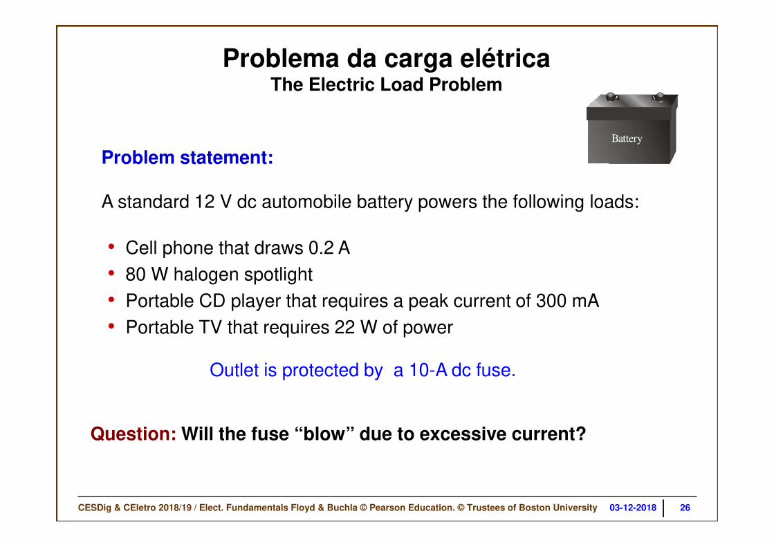
Problema da carga elétricaThe Electric Load Problem
Problem statement:
A standard 12 V dc automobile battery powers the following loads:
• Cell phone that draws 0.2 A• 80 W halogen spotlight• Portable CD player that requires a peak current of 300 mA• Portable TV that requires 22 W of power
Question: Will the fuse “blow” due to excessive current?
Outlet is protected by a 10-A dc fuse.
26
Battery
CESDig & CEletro 2018/19 / Elect. Fundamentals Floyd & Buchla © Pearson Education. © Trustees of Boston University 03-12-2018
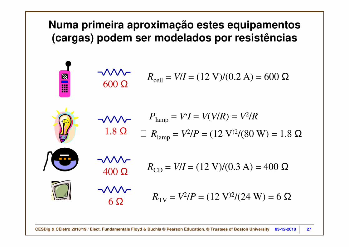
Numa primeira aproximação estes equipamentos (cargas) podem ser modelados por resistências
Rcell = V/I = (12 V)/(0.2 A) = 600 Ω600 Ω
∴ Rlamp = V2/P = (12 V)2/(80 W) = 1.8 Ω
Plamp = V.I = V(V/R) = V2/R
1.8 Ω
RCD = V/I = (12 V)/(0.3 A) = 400 Ω400 Ω
RTV = V2/P = (12 V)2/(24 W) = 6 Ω6 Ω
27

CESDig & CEletro 2018/19 / Elect. Fundamentals Floyd & Buchla © Pearson Education. © Trustees of Boston University 03-12-2018
All of the loads are connected in parallel.
Rcell = 600 Ω
Rlamp = 1.8 Ω
RCD = 400 Ω
RTV = 6 Ω
Draw the schematic of the entire circuit:
FUSE
+_ VBAT =12 V
Outlet is protected by a 10-A dc fuse.
Esquema grosseiro do circuito
28

CESDig & CEletro 2018/19 / Elect. Fundamentals Floyd & Buchla © Pearson Education. © Trustees of Boston University 03-12-2018
A simpler way to view the circuit:
Use the formula for resistors connected in parallel:
1 1 1 1 1——— = ––– + ––– + ––– + –––
Requiv Rcell Rlamp RCD RTV
(Add the conductances):
= 1/(600 Ω) + 1/(1.8 Ω) + 1/(400 Ω) + 1/(6 Ω) = 0.726 Ω–1
Requiv = 1/(0.726 Ω–1) = 1.38 Ω
+_ VBAT 12 V Rcell RTVRCDRlamp
10 A FUSE
Requiv
Esquema do circuito
29
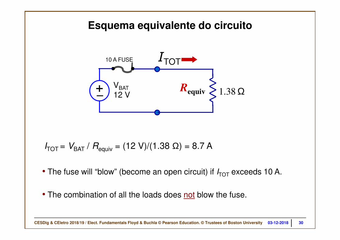
CESDig & CEletro 2018/19 / Elect. Fundamentals Floyd & Buchla © Pearson Education. © Trustees of Boston University 03-12-2018
+_VBAT 12 V
Requiv 1.38 Ω
ITOT
ITOT = VBAT / Requiv = (12 V)/(1.38 Ω) = 8.7 A
• The fuse will “blow” (become an open circuit) if ITOT exceeds 10 A.
10 A FUSE
• The combination of all the loads does not blow the fuse.
Esquema equivalente do circuito
30

CESDig & CEletro 2018/19 / Elect. Fundamentals Floyd & Buchla © Pearson Education. © Trustees of Boston University 03-12-2018
Problema da potência fornecida aos altifalantes
Problem:
• Public address amplifier powers loudspeakers as shown below. • Amplifier produces an average voltage of 11.3 V.
Question: How much power does each speaker receive?
S1
S2
S3
S4
S5
S6
S1 = 8 ΩS2 = 16 ΩS3 = 8 ΩS4 = 4 ΩS5 = 4 ΩS6 = 8 Ω
Amplifier
11.3 V
31

CESDig & CEletro 2018/19 / Elect. Fundamentals Floyd & Buchla © Pearson Education. © Trustees of Boston University 03-12-2018
Model the system by a resistive circuit:
11.3 VVamp
<
R1 = 8 Ω
R2 = 16 Ω
R3 = 8 Ω
R4 = 4 Ω
R5 = 4 Ω
R6 = 8 Ω
i1
i2
i3
i4
i5
i6
• The power to any given speaker will be i2R
• Use KVL and KCL to find the various values of in
S1
S2
S3
S4
S5
S6
Altifalantes podem ser representados por resistências
32

CESDig & CEletro 2018/19 / Elect. Fundamentals Floyd & Buchla © Pearson Education. © Trustees of Boston University 03-12-2018
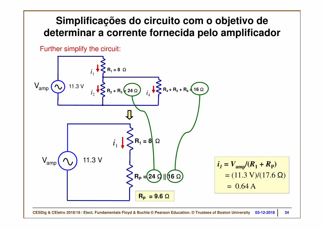
Simplify the circuit as follows:
11.3 VVamp
R1 = 8 Ω
R2 = 16 Ω
R3 = 8 Ω
R4 = 4 Ω
R5 = 4 Ω
R6 = 8 Ω
i2 i4R4 + R5 + R6 = 16 Ω
R1 = 8 Ωi1
11.3 V
Vamp R2 + R3 = 24 Ω
Simplificações do circuito com o objetivo de determinar a corrente fornecida pelo amplificador
33
CESDig & CEletro 2018/19 / Elect. Fundamentals Floyd & Buchla © Pearson Education. © Trustees of Boston University 03-12-2018
Further simplify the circuit:
RP = 24 Ω || 16 Ω
R1 = 8 Ωi1
11.3 VVamp
R2 + R3 = 24 Ω R4 + R5 + R6 = 16 Ωi2 i4
R1 = 8 Ωi1
11.3 VVamp
i1 = Vamp/(R1 + RP)
= (11.3 V)/(17.6 Ω)
= 0.64 A
RP = 9.6 Ω
Simplificações do circuito com o objetivo de determinar a corrente fornecida pelo amplificador
34

CESDig & CEletro 2018/19 / Elect. Fundamentals Floyd & Buchla © Pearson Education. © Trustees of Boston University 03-12-2018
RB =R4+R5+R6 = 16 ΩRA = R2+R3 = 24 Ωi2i4
R1 = 8 Ωi1= 0.64 A
11.3 V
Vamp
Now use current division to find i2 and i4:
Current Division
i4
RA 24 Ωi4 = i1 = 0.64 A = 0.38 A
RA + RB 24 Ω + 16 ΩSimilarly:
RB 16 Ωi2 = i1 = 0.64 A = 0.26 A
RA + RB 24 Ω + 16 ΩCurrent Division:
Note that: i2 + i4 = 0.26 A + 0.38 A = 0.64 A
Determinação das correntes nos ramos
35

CESDig & CEletro 2018/19 / Elect. Fundamentals Floyd & Buchla © Pearson Education. © Trustees of Boston University 03-12-2018
KCL
KCL11.3 VVamp
R1 = 8 Ω
R2 = 16 Ω
R3 = 8 Ω
R4 = 4 Ω
R5 = 4 Ω
R6 = 8 Ω
i2 = 0.26 A
i1= 0.64 A
i3 = 0.26 A
i4 = 0.38 A
i5 = 0.38 A
i6 = 0.38 A
KCL
Now find all the currents in the circuit:
Determinação das correntes em cada ramo
36

CESDig & CEletro 2018/19 / Elect. Fundamentals Floyd & Buchla © Pearson Education. © Trustees of Boston University 03-12-2018
Given:
S1 = 8 ΩS2 = 16 ΩS3 = 8 ΩS4 = 4 ΩS5 = 4 ΩS6 = 8 Ω
S1
S2
S3
S4
S5
S6
Amplifier
11.3 V
Find the power into each speaker using i2R:
P1 = i12R1 = (0.64 A)2(8 Ω) = 3.28 W
Currents:
i1= 0.64 A
i2 = i3 = 0.26 A
i4 = i5 = i6 = 0.38 A P2 = i2
2R2 = (0.26 A)2(16 Ω) = 1.08 W
P3 = i32R3 = (0.26 A)2(8 Ω) = 0.54 W
P4 = i42R4 = (0.38 A)2(4 Ω) = 0.58 W
P5 = i52R5 = (0.38 A)2(4 Ω) = 0.58 W
P6 = i62R6 = (0.38 A)2(8 Ω) = 1.16 W
Solutions:
+ = 7.22 W
V• i1 = (11.3 V)(0.64 A) = 7.22 W
Determinação das potências fornecidas aos altifalantes
37

CESDig & CEletro 2018/19 / Elect. Fundamentals Floyd & Buchla © Pearson Education. © Trustees of Boston University 03-12-2018
Atenuador resistivo
38

CESDig & CEletro 2018/19 / Elect. Fundamentals Floyd & Buchla © Pearson Education. © Trustees of Boston University 03-12-2018
R1 R1
R1 R1
R2 R2
+vin
–
+vout
–
Objetivo: determinar a razão de atenuação vout/vin
Let’s go over the steps…
• Use voltage division to find vout
• Find voltage v2
+v2
–
Atenuador resistivo
39

CESDig & CEletro 2018/19 / Elect. Fundamentals Floyd & Buchla © Pearson Education. © Trustees of Boston University 03-12-2018 40
R1 R1
R1 R1
R2 R2
+vin
–
+vout
–
+v2
–
• Find voltage v2
R1
R1
R2
+vin
–2R1+ R2
+vout–
Atenuador resistivo

CESDig & CEletro 2018/19 / Elect. Fundamentals Floyd & Buchla © Pearson Education. © Trustees of Boston University 03-12-2018 41
• Find voltage v2
R1
R1
R2
+vin
–2R1+ R2
R1
R1
+vin
–RP = R2 || (2R1+ R2)
+
v2
–
+
v2
–
v2 =RP
RP + 2R1vin
Atenuador resistivo

CESDig & CEletro 2018/19 / Elect. Fundamentals Floyd & Buchla © Pearson Education. © Trustees of Boston University 03-12-2018
R1 R1
R1 R1
R2 R2
+vin
–
+vout
–
+v2
–
v2 =RP
RP + 2R1vin
Voltando ao circuito original
vout =R2
R2 + 2R1v2 =
R2R2 + 2R1
vin
RPRp + 2R1
=R2
R2 + 2R1vin
RPRp + 2R1
vout
Attenuation Factors
Atenuador resistivo
42
RP = R2 || (2R1+ R2)
CESDig & CEletro 2018/19 / Elect. Fundamentals Floyd & Buchla © Pearson Education. © Trustees of Boston University 03-12-2018
Amplificadores com transístores
43

CESDig & CEletro 2018/19 / Elect. Fundamentals Floyd & Buchla © Pearson Education. © Trustees of Boston University 03-12-2018
+_VBB
vs
RB
RC
+
_vOUTinput
Output
+VCC
–
BC
E
Transistor Amplifier
Amplificador com transístor I(para rever)
44
CESDig & CEletro 2018/19 / Elect. Fundamentals Floyd & Buchla © Pearson Education. © Trustees of Boston University 03-12-2018 45
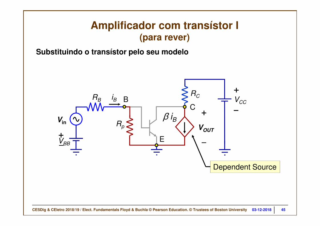
Substituindo o transístor pelo seu modelo
RC
+
_
VOUT
RB
+_VBB
Vin
Dependent Source
+VCC
–
Rp
β iB
iB BC
Amplificador com transístor I(para rever)
E

CESDig & CEletro 2018/19 / Elect. Fundamentals Floyd & Buchla © Pearson Education. © Trustees of Boston University 03-12-2018
Find iB: RC
+
_VOUT
RB
+_VBB
vs
Dependent Source
Rpβ iB
iB
KVL: VBB + vs = iB (RB + Rp) RB + Rp
VBB + vsiB =
We know iB Find vOUT
KVL
+VCC
–
Amplificador com transístor I(para rever)
46
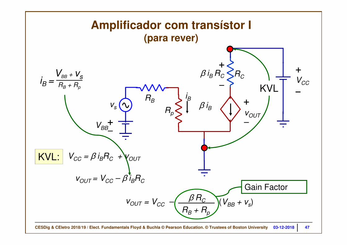
CESDig & CEletro 2018/19 / Elect. Fundamentals Floyd & Buchla © Pearson Education. © Trustees of Boston University 03-12-2018
RB + Rp
VBB + vsiB =
RC
RB
+_VBB
vs Rp
β iB
iB +
_vOUT
+VCC
–
KVL: VCC = β iBRC + vOUT
+
_β iB RC
vOUT = VCC – β iBRC
β RC
RB + Rp
(VBB + vs)
Gain Factor
KVL
Amplificador com transístor I(para rever)
= VCC –vOUT
47

CESDig & CEletro 2018/19 / Elect. Fundamentals Floyd & Buchla © Pearson Education. © Trustees of Boston University 03-12-2018
vs
vOUT
VCC
β RC
RB + Rp
(VBB + vs)vOUT
Fator de ganho
VCC –RB + Rp
β RC
VBBSlope = –β RC /(RB + Rp)
Amplificador com transístor I(para rever)
= VCC –
48
CESDig & CEletro 2018/19 / Elect. Fundamentals Floyd & Buchla © Pearson Education. © Trustees of Boston University 03-12-2018
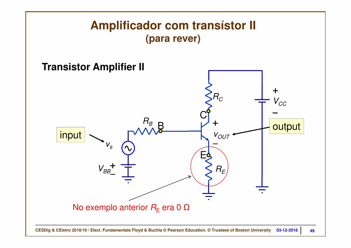
+_VBB
vs
RB
RC
RE
+
_vOUTinput
output
+VCC
–
Transistor Amplifier II
C
E
B
49
Amplificador com transístor II(para rever)
No exemplo anterior RE era 0 Ω

CESDig & CEletro 2018/19 / Elect. Fundamentals Floyd & Buchla © Pearson Education. © Trustees of Boston University 03-12-2018
Substitute the transistor model:
RE
RC
+
_vOUT
RB
+_VBB
vs
Dependent source
Rp βiBiB
+VCC
–
Amplificador com transístor II(para rever)
No exemplo anterior RE era 0 Ω
50
CESDig & CEletro 2018/19 / Elect. Fundamentals Floyd & Buchla © Pearson Education. © Trustees of Boston University 03-12-2018 51
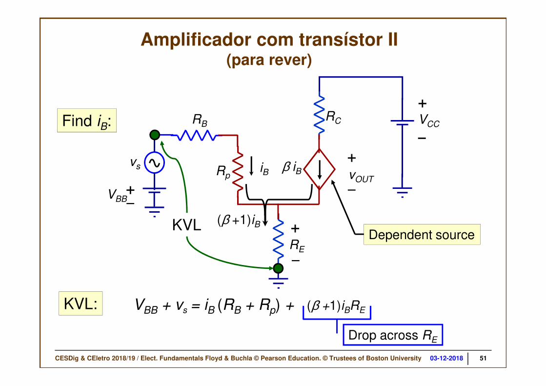
Find iB:
RE
RC
+
_vOUT
RB
+_VBB
vs
Dependent source
Rpβ iBiB
KVL
KVL: VBB + vs = iB (RB + Rp) + (β +1)iBRE
Drop across RE
(β +1)iB +
_
+VCC
–
Amplificador com transístor II(para rever)

CESDig & CEletro 2018/19 / Elect. Fundamentals Floyd & Buchla © Pearson Education. © Trustees of Boston University 03-12-2018
VBB + vs = iB(RB + Rp) + (β +1)iBRE RB + Rp + (β +1)RE
VBB + vsiB =
We know iB Find vOUT
RCRB
+_VBB
vs
RE
Rp
β iB
iB +
_vOUT
+VCC
–
Amplificador com transístor II(para rever)
52
CESDig & CEletro 2018/19 / Elect. Fundamentals Floyd & Buchla © Pearson Education. © Trustees of Boston University 03-12-2018
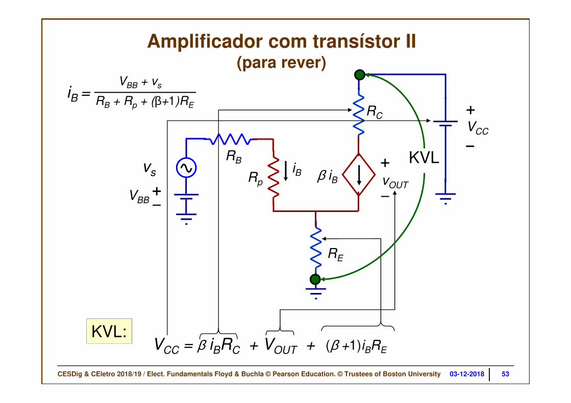
RB + Rp + (β+1)RE
VBB + vsiB =
RC
RB
+_VBB
vs
RE
Rpβ iB
iB+
_vOUT
KVL
+VCC
–
KVL:VCC = β iBRC + VOUT + (β +1)iBRE
Amplificador com transístor II(para rever)
53

CESDig & CEletro 2018/19 / Elect. Fundamentals Floyd & Buchla © Pearson Education. © Trustees of Boston University 03-12-2018
VCC = β iBRC + VOUT + (β +1)iBRE
Solve for vOUT
vOUT = VCC – [ β iBRC + (β +1)iBRE ]
= VCC – iB [β RC + (β +1)RE ]
vOUT = VCC – (VBB + vs) RB + Rp + (β +1)RE
β RC + (β +1)RE
Fator de ganho
(from output loop)
RB + Rp + (β +1)RE
VBB + vsiB =
(from input loop)
Amplificador com transístor II(para rever)
54
CESDig & CEletro 2018/19 / Elect. Fundamentals Floyd & Buchla © Pearson Education. © Trustees of Boston University 03-12-2018
Circuitos com potenciómetros
55
CESDig & CEletro 2018/19 / Elect. Fundamentals Floyd & Buchla © Pearson Education. © Trustees of Boston University 03-12-2018
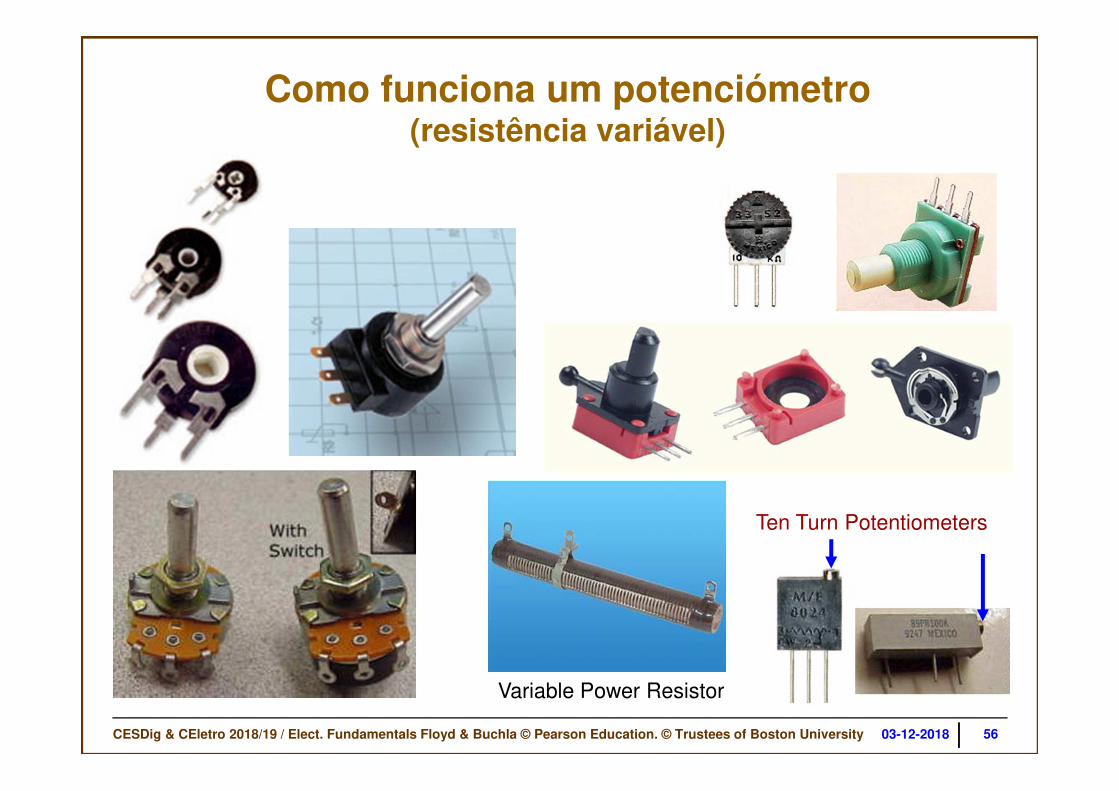
Como funciona um potenciómetro (resistência variável)
Variable Power Resistor
Ten Turn Potentiometers
56
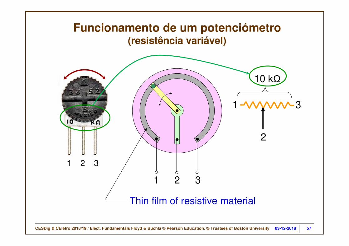
CESDig & CEletro 2018/19 / Elect. Fundamentals Floyd & Buchla © Pearson Education. © Trustees of Boston University 03-12-2018 57
1 2 3
1
2
3
10 kΩ
1 2 3
Thin film of resistive material
Funcionamento de um potenciómetro (resistência variável)

CESDig & CEletro 2018/19 / Elect. Fundamentals Floyd & Buchla © Pearson Education. © Trustees of Boston University 03-12-2018 58
1 2 3
1 3 RTOT
Potenciómetro como divisor resistivo
1 2 3
1 3 RTOT
2
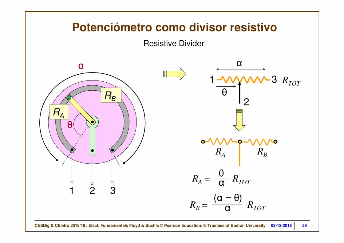
CESDig & CEletro 2018/19 / Elect. Fundamentals Floyd & Buchla © Pearson Education. © Trustees of Boston University 03-12-2018 59
1 2 3
α
Resistive Divider
RA
RB
RA
= RTOT
θα
RB
= RTOT
(α − θ)α
RA
RB
1 3
α
θR
TOT
2
θ
Potenciómetro como divisor resistivo

CESDig & CEletro 2018/19 / Elect. Fundamentals Floyd & Buchla © Pearson Education. © Trustees of Boston University 03-12-2018 •60
vin +v1
–
A v1Loudspeakerload
Volume Control Dependent Source
Uso do potenciómetro para controlar o volume de um amplificador de som
Vin αθ V1= (θ/α)Vin
RA
RB
v1 = Vin
= Vin
RA
RA
+ RB
RA
RTOT
v1 = Vinθα
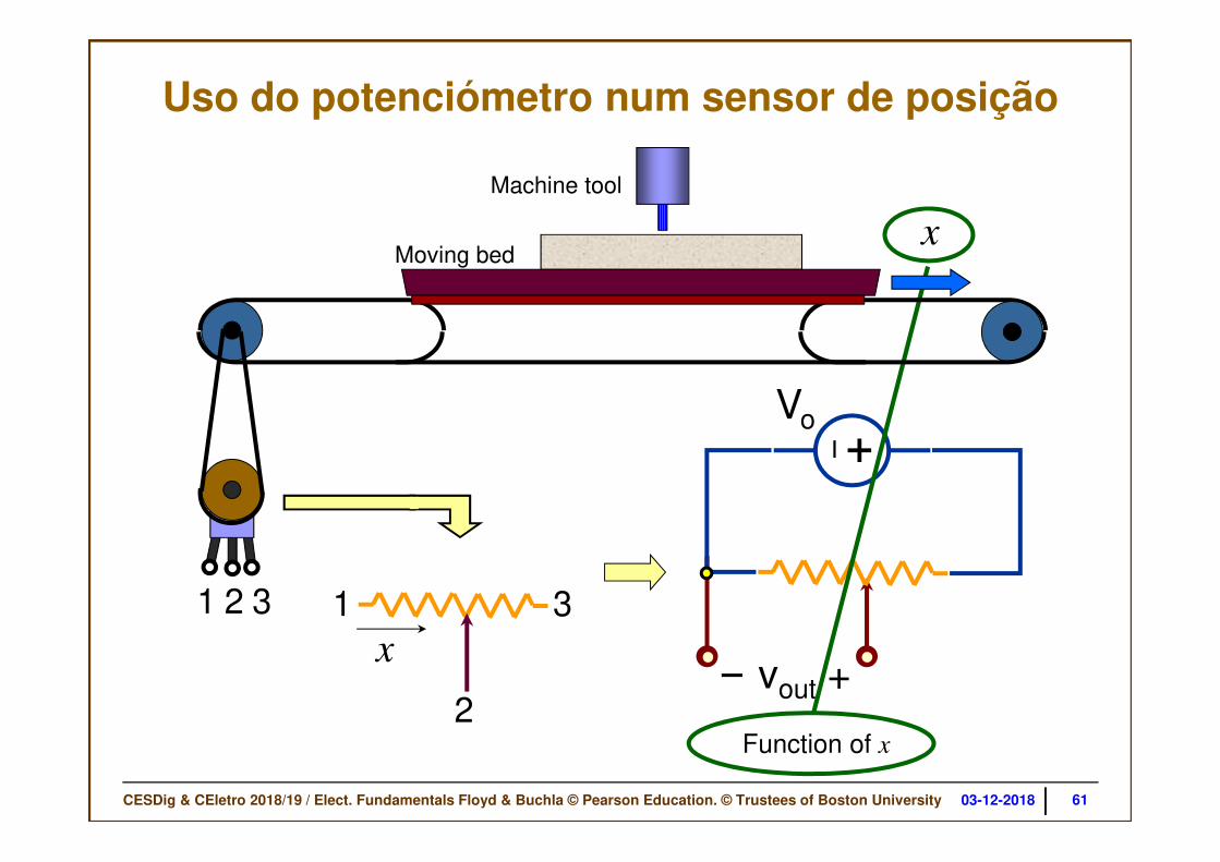
CESDig & CEletro 2018/19 / Elect. Fundamentals Floyd & Buchla © Pearson Education. © Trustees of Boston University 03-12-2018
1 3x
2
+_Vo
vout +
Function of x
1 2 3
x
Machine tool
Moving bed
Uso do potenciómetro num sensor de posição
61

CESDig & CEletro 2018/19 / Elect. Fundamentals Floyd & Buchla © Pearson Education. © Trustees of Boston University 03-12-2018
Rede R-2R / R-2R Ladder Network
(componente de conversor digital-analógico simples)
62

CESDig & CEletro 2018/19 / Elect. Fundamentals Floyd & Buchla © Pearson Education. © Trustees of Boston University 03-12-2018
Logic 0 Logic 1
R R
R2R 2R 2R 2R 2R 2R
D0 D1 D2 D3
Digital Inputs
Analog Output
VREF
Conversor digital-analógico simples
Rede R-2R / R-2R Ladder Network
Num conversor prático o interruptor é substituído por um transístor.
63

CESDig & CEletro 2018/19 / Elect. Fundamentals Floyd & Buchla © Pearson Education. © Trustees of Boston University 03-12-2018
R R R
2R 2R 2 R 2R 2R 2R
Analog Output
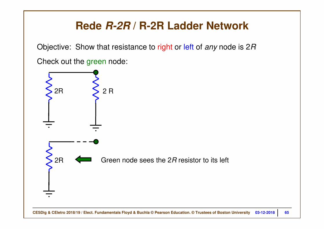
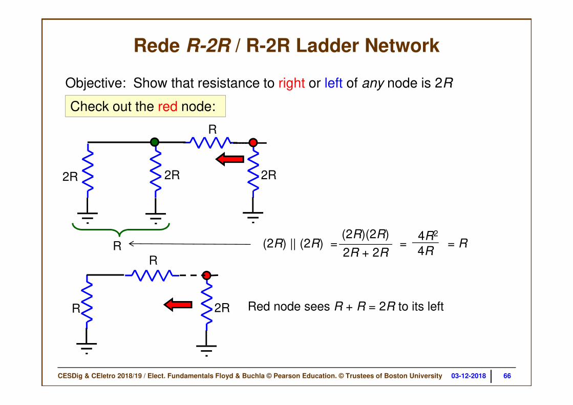
Objective: Show that resistance to right or left of any node is 2R
Specific value of R does not matter
Req
Req
Rede R-2R / R-2R Ladder Network
64
CESDig & CEletro 2018/19 / Elect. Fundamentals Floyd & Buchla © Pearson Education. © Trustees of Boston University 03-12-2018
2R 2 R
Objective: Show that resistance to right or left of any node is 2R
Check out the green node:
Rede R-2R / R-2R Ladder Network
2R Green node sees the 2R resistor to its left
65
CESDig & CEletro 2018/19 / Elect. Fundamentals Floyd & Buchla © Pearson Education. © Trustees of Boston University 03-12-2018 66
R
2R 2R 2R
Check out the red node:
Red node sees R + R = 2R to its left
(2R)(2R)
2R + 2R= = R
4R2
4R(2R) || (2R) =
Objective: Show that resistance to right or left of any node is 2R
Rede R-2R / R-2R Ladder Network
R
2RR
R
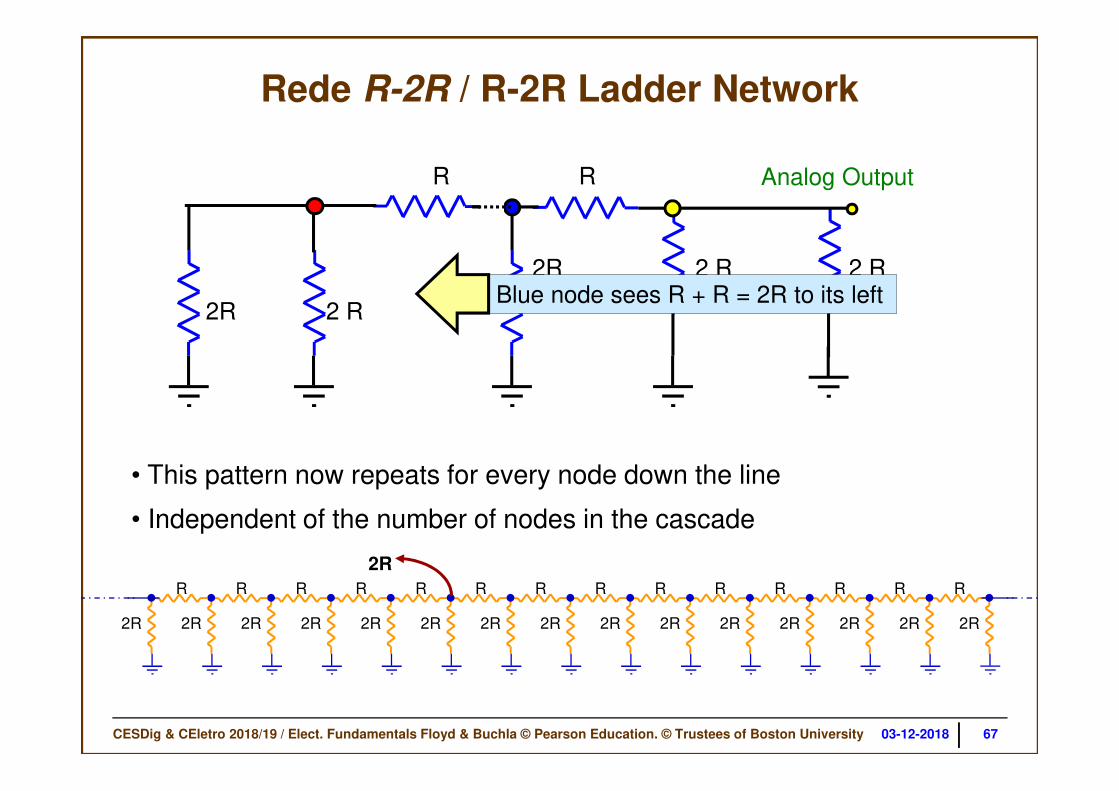
CESDig & CEletro 2018/19 / Elect. Fundamentals Floyd & Buchla © Pearson Education. © Trustees of Boston University 03-12-2018 67
R R
2R 2 R
2R 2 R 2 R
Analog Output
• This pattern now repeats for every node down the line
• Independent of the number of nodes in the cascade
R
2R
R
2R
R
2R
R
2R
R
2R
R
2R
R
2R
R
2R
R
2R
R
2R
R
2R 2R
R
2R
R
2R
R
2R
2R
Blue node sees R + R = 2R to its left
Rede R-2R / R-2R Ladder Network
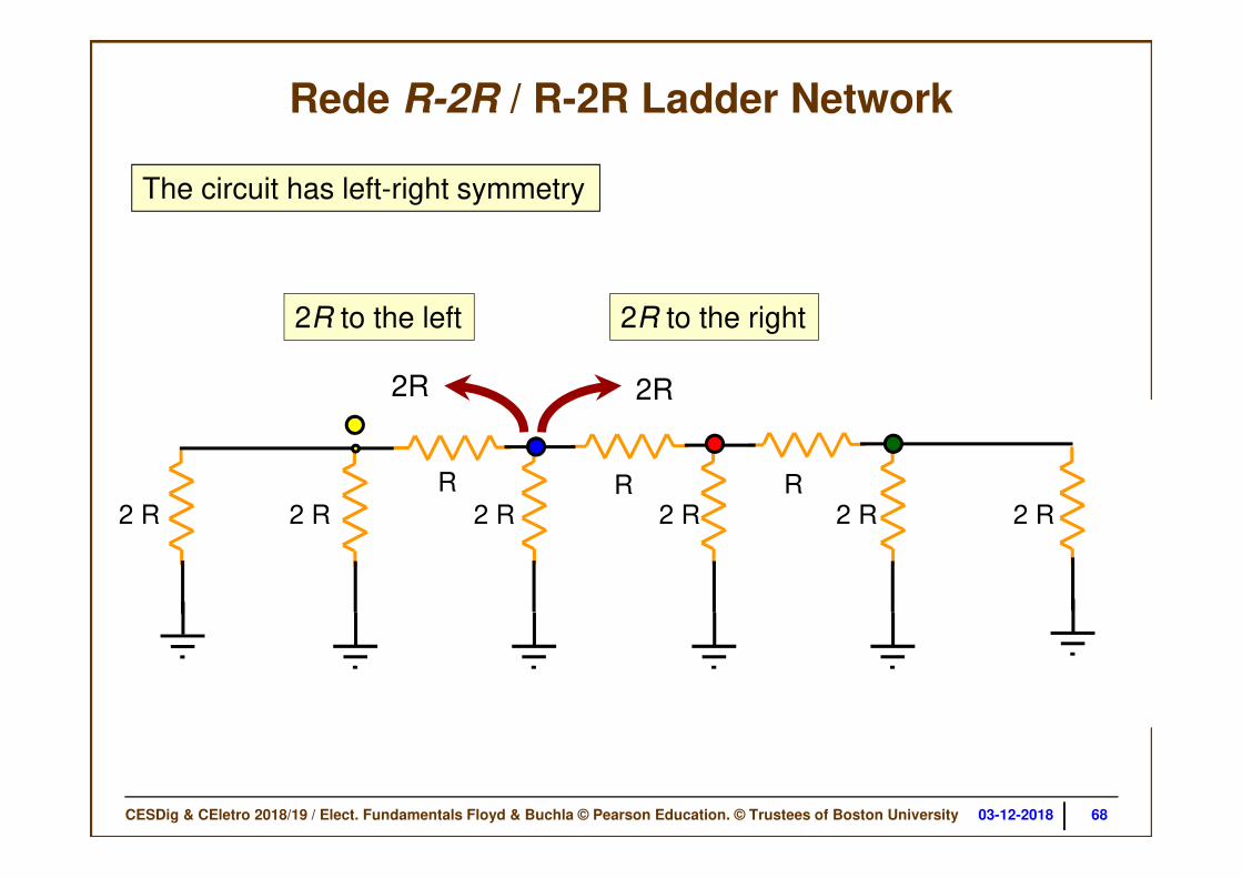
CESDig & CEletro 2018/19 / Elect. Fundamentals Floyd & Buchla © Pearson Education. © Trustees of Boston University 03-12-2018 68
2 R 2 R 2 R 2 R 2 R 2 RRRR
2 R2 R2 R2 R2 R2 R
The circuit has left-right symmetry
2R 2R
2R to the left 2R to the right
Rede R-2R / R-2R Ladder Network
Recommended