Chapter 4 – Combinational Logic Circuits
Copyright © 2011, 2007, 2004, 2001, 1998 by Pearson Education, Inc.
Upper Saddle River, New Jersey 07458 • All rights reserved Digital Systems: Principles and Applications, 11/e
Ronald J. Tocci, Neal S. Widmer, Gregory L. Moss
• Selected areas covered in this chapter:
– Converting logic expressions to sum-of-products
expressions.
– Boolean algebra and the Karnaugh map as tools to
simplify and design logic circuits.
– Operation of exclusive-OR & exclusive-NOR circuits.
– Designing simple logic circuits without a truth table.
– Basic characteristics of TTL and CMOS digital ICs.
– Basic troubleshooting rules of digital systems.
– Programmable logic device (PLD) fundamentals.
– Hierarchical design methods.
– Logic circuits using HDL control structures IF/ELSE,
IF/ELSIF, and CASE.
Chapter 4 Objectives
Copyright © 2011, 2007, 2004, 2001, 1998 by Pearson Education, Inc.
Upper Saddle River, New Jersey 07458 • All rights reserved Digital Systems: Principles and Applications, 11/e
Ronald J. Tocci, Neal S. Widmer, Gregory L. Moss
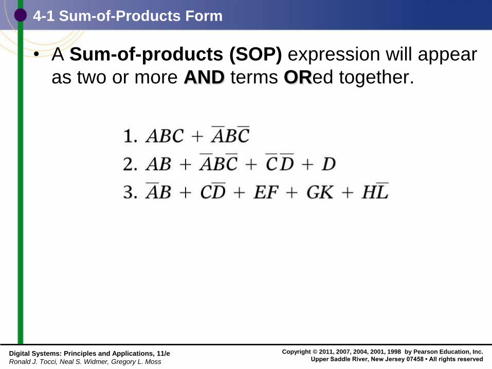
4-1 Sum-of-Products Form
• A Sum-of-products (SOP) expression will appear
as two or more AND terms ORed together.
Copyright © 2011, 2007, 2004, 2001, 1998 by Pearson Education, Inc.
Upper Saddle River, New Jersey 07458 • All rights reserved Digital Systems: Principles and Applications, 11/e
Ronald J. Tocci, Neal S. Widmer, Gregory L. Moss
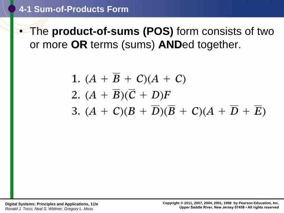
4-1 Sum-of-Products Form
• The product-of-sums (POS) form consists of two
or more OR terms (sums) ANDed together.
Copyright © 2011, 2007, 2004, 2001, 1998 by Pearson Education, Inc.
Upper Saddle River, New Jersey 07458 • All rights reserved Digital Systems: Principles and Applications, 11/e
Ronald J. Tocci, Neal S. Widmer, Gregory L. Moss
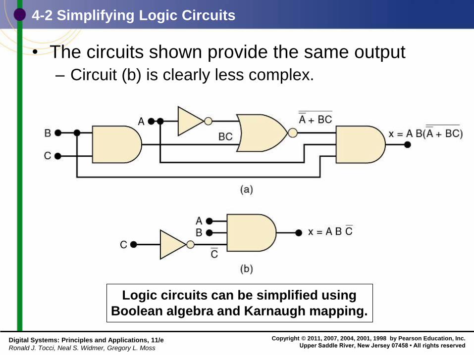
• The circuits shown provide the same output
– Circuit (b) is clearly less complex.
4-2 Simplifying Logic Circuits
Logic circuits can be simplified using
Boolean algebra and Karnaugh mapping.
Copyright © 2011, 2007, 2004, 2001, 1998 by Pearson Education, Inc.
Upper Saddle River, New Jersey 07458 • All rights reserved Digital Systems: Principles and Applications, 11/e
Ronald J. Tocci, Neal S. Widmer, Gregory L. Moss
4-3 Algebraic Simplification
• Place the expression in SOP form by applying
DeMorgan’s theorems and multiplying terms.
• Check the SOP form for common factors.
– Factoring where possible should eliminate one
or more terms.
Copyright © 2011, 2007, 2004, 2001, 1998 by Pearson Education, Inc.
Upper Saddle River, New Jersey 07458 • All rights reserved Digital Systems: Principles and Applications, 11/e
Ronald J. Tocci, Neal S. Widmer, Gregory L. Moss
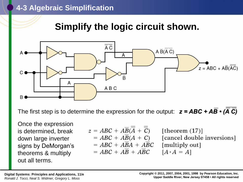
4-3 Algebraic Simplification
Simplify the logic circuit shown.
The first step is to determine the expression for the output: z = ABC + AB • (A C)
Once the expression
is determined, break
down large inverter
signs by DeMorgan’s
theorems & multiply
out all terms.
Copyright © 2011, 2007, 2004, 2001, 1998 by Pearson Education, Inc.
Upper Saddle River, New Jersey 07458 • All rights reserved Digital Systems: Principles and Applications, 11/e
Ronald J. Tocci, Neal S. Widmer, Gregory L. Moss
4-3 Algebraic Simplification
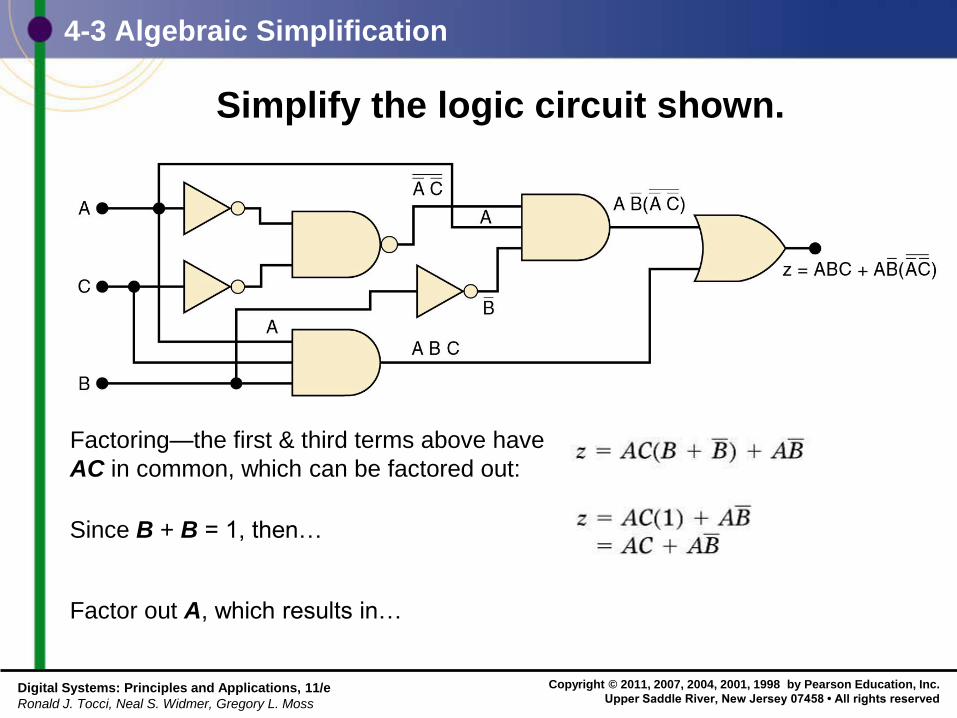
Simplify the logic circuit shown.
Factoring—the first & third terms above have
AC in common, which can be factored out:
Since B + B = 1, then…
Factor out A, which results in…
Copyright © 2011, 2007, 2004, 2001, 1998 by Pearson Education, Inc.
Upper Saddle River, New Jersey 07458 • All rights reserved Digital Systems: Principles and Applications, 11/e
Ronald J. Tocci, Neal S. Widmer, Gregory L. Moss
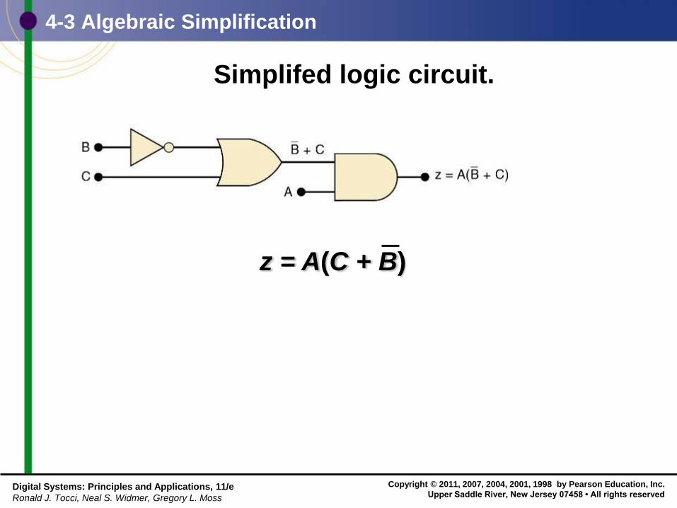
4-3 Algebraic Simplification
Simplifed logic circuit.
z = A(C + B)
Copyright © 2011, 2007, 2004, 2001, 1998 by Pearson Education, Inc.
Upper Saddle River, New Jersey 07458 • All rights reserved Digital Systems: Principles and Applications, 11/e
Ronald J. Tocci, Neal S. Widmer, Gregory L. Moss
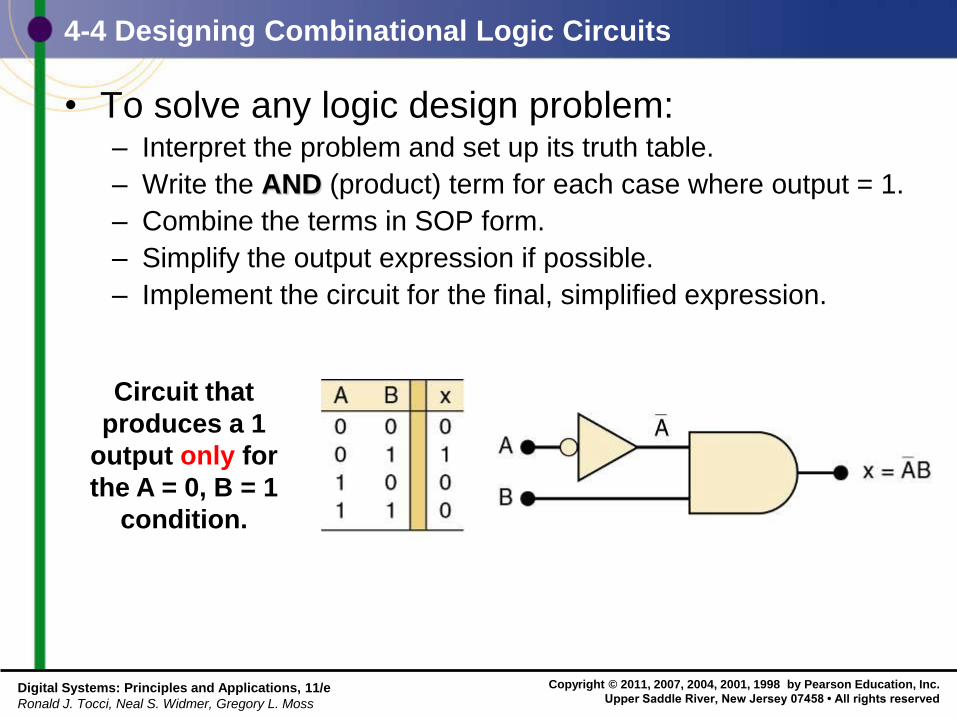
4-4 Designing Combinational Logic Circuits
• To solve any logic design problem: – Interpret the problem and set up its truth table.
– Write the AND (product) term for each case where output = 1.
– Combine the terms in SOP form.
– Simplify the output expression if possible.
– Implement the circuit for the final, simplified expression.
Circuit that
produces a 1
output only for
the A = 0, B = 1
condition.
Copyright © 2011, 2007, 2004, 2001, 1998 by Pearson Education, Inc.
Upper Saddle River, New Jersey 07458 • All rights reserved Digital Systems: Principles and Applications, 11/e
Ronald J. Tocci, Neal S. Widmer, Gregory L. Moss
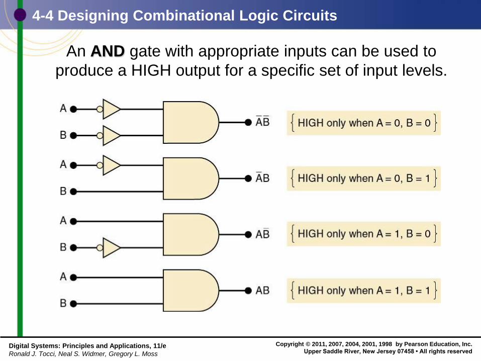
4-4 Designing Combinational Logic Circuits
An AND gate with appropriate inputs can be used to
produce a HIGH output for a specific set of input levels.
Copyright © 2011, 2007, 2004, 2001, 1998 by Pearson Education, Inc.
Upper Saddle River, New Jersey 07458 • All rights reserved Digital Systems: Principles and Applications, 11/e
Ronald J. Tocci, Neal S. Widmer, Gregory L. Moss
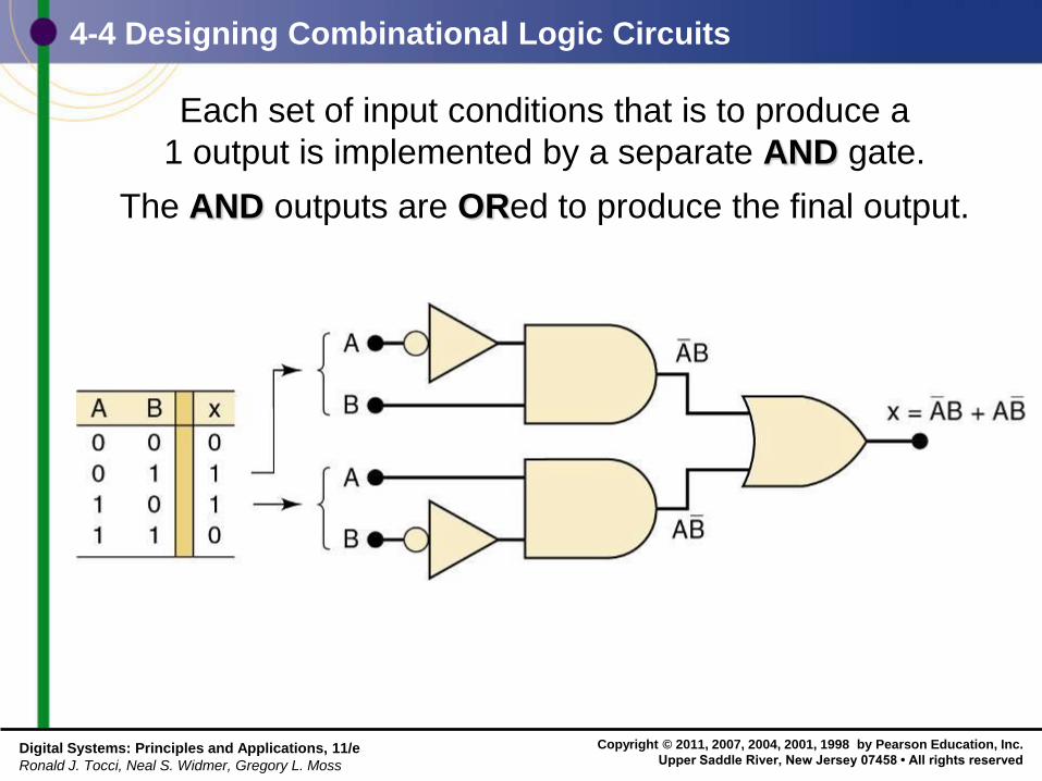
4-4 Designing Combinational Logic Circuits
Each set of input conditions that is to produce a
1 output is implemented by a separate AND gate.
The AND outputs are ORed to produce the final output.
Copyright © 2011, 2007, 2004, 2001, 1998 by Pearson Education, Inc.
Upper Saddle River, New Jersey 07458 • All rights reserved Digital Systems: Principles and Applications, 11/e
Ronald J. Tocci, Neal S. Widmer, Gregory L. Moss
4-4 Designing Combinational Logic Circuits
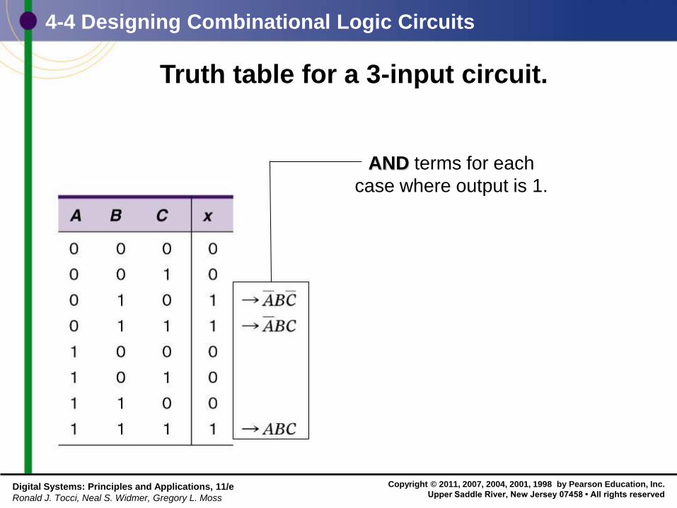
Truth table for a 3-input circuit.
AND terms for each
case where output is 1.
Copyright © 2011, 2007, 2004, 2001, 1998 by Pearson Education, Inc.
Upper Saddle River, New Jersey 07458 • All rights reserved Digital Systems: Principles and Applications, 11/e
Ronald J. Tocci, Neal S. Widmer, Gregory L. Moss
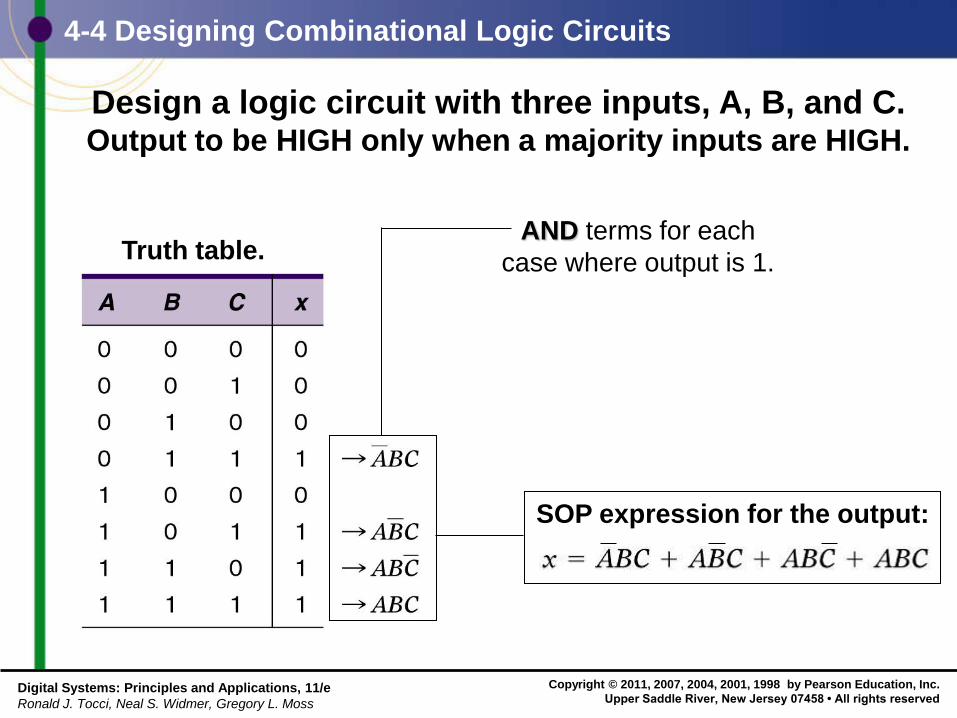
4-4 Designing Combinational Logic Circuits
Design a logic circuit with three inputs, A, B, and C. Output to be HIGH only when a majority inputs are HIGH.
Truth table. AND terms for each
case where output is 1.
SOP expression for the output:
Copyright © 2011, 2007, 2004, 2001, 1998 by Pearson Education, Inc.
Upper Saddle River, New Jersey 07458 • All rights reserved Digital Systems: Principles and Applications, 11/e
Ronald J. Tocci, Neal S. Widmer, Gregory L. Moss
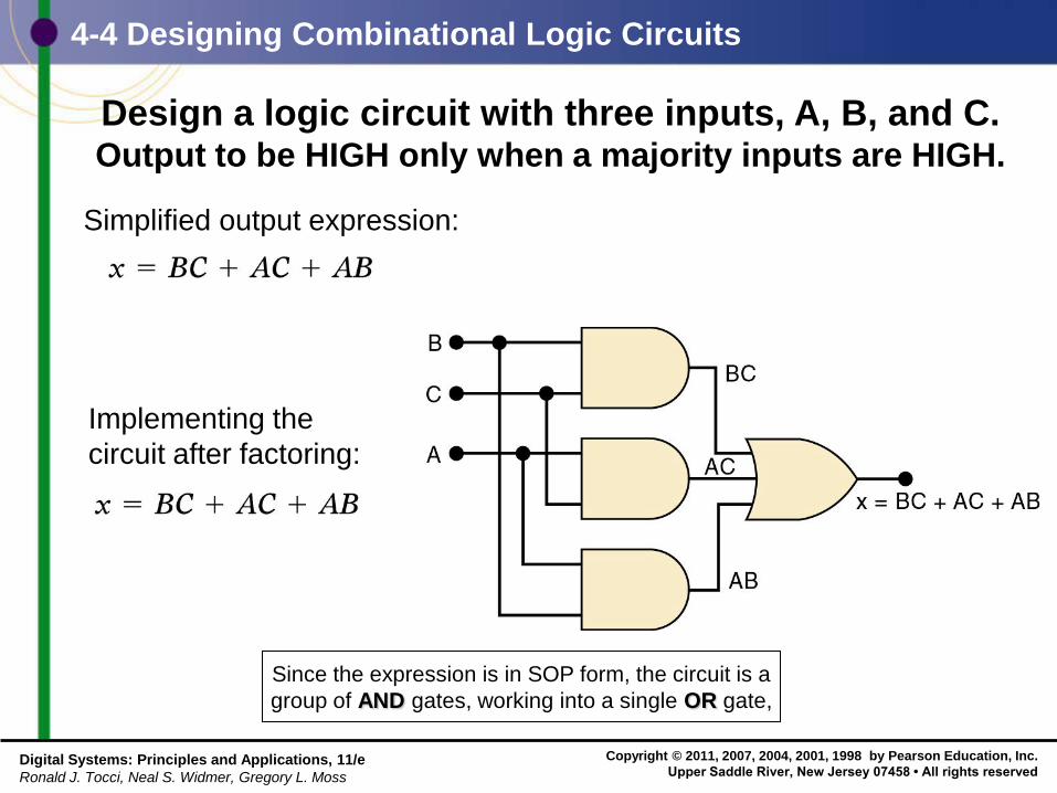
4-4 Designing Combinational Logic Circuits
Design a logic circuit with three inputs, A, B, and C. Output to be HIGH only when a majority inputs are HIGH.
Simplified output expression:
Implementing the
circuit after factoring:
Since the expression is in SOP form, the circuit is a
group of AND gates, working into a single OR gate,
Copyright © 2011, 2007, 2004, 2001, 1998 by Pearson Education, Inc.
Upper Saddle River, New Jersey 07458 • All rights reserved Digital Systems: Principles and Applications, 11/e
Ronald J. Tocci, Neal S. Widmer, Gregory L. Moss
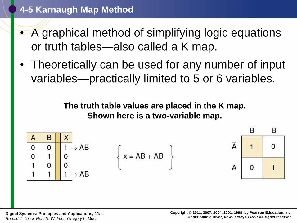
4-5 Karnaugh Map Method
• A graphical method of simplifying logic equations
or truth tables—also called a K map.
• Theoretically can be used for any number of input
variables—practically limited to 5 or 6 variables.
The truth table values are placed in the K map.
Shown here is a two-variable map.
Copyright © 2011, 2007, 2004, 2001, 1998 by Pearson Education, Inc.
Upper Saddle River, New Jersey 07458 • All rights reserved Digital Systems: Principles and Applications, 11/e
Ronald J. Tocci, Neal S. Widmer, Gregory L. Moss
4-5 Karnaugh Map Method
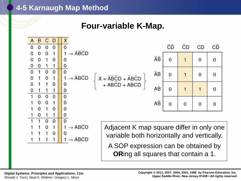
Four-variable K-Map.
Adjacent K map square differ in only one
variable both horizontally and vertically.
A SOP expression can be obtained by
ORing all squares that contain a 1.
Copyright © 2011, 2007, 2004, 2001, 1998 by Pearson Education, Inc.
Upper Saddle River, New Jersey 07458 • All rights reserved Digital Systems: Principles and Applications, 11/e
Ronald J. Tocci, Neal S. Widmer, Gregory L. Moss
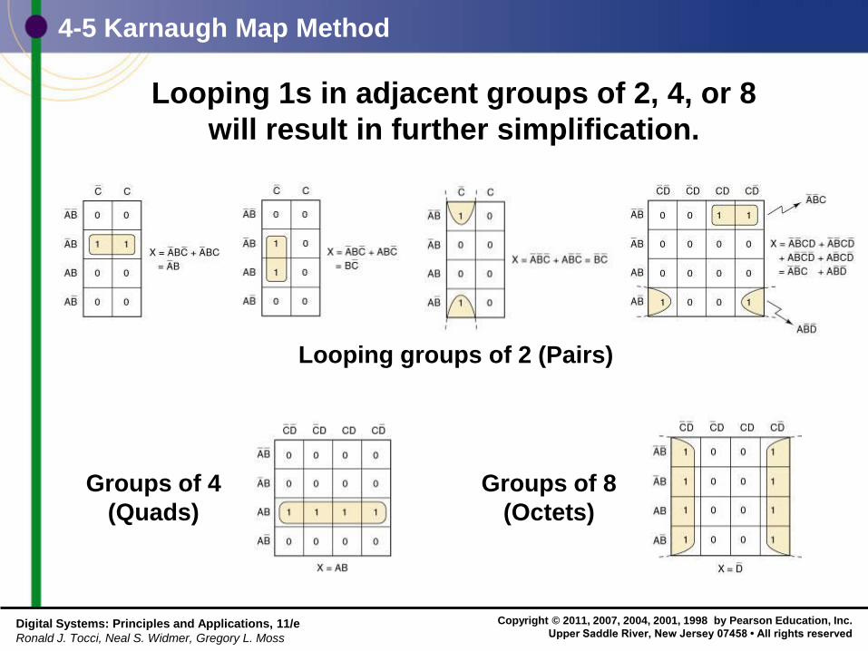
4-5 Karnaugh Map Method
Looping 1s in adjacent groups of 2, 4, or 8
will result in further simplification.
Looping groups of 2 (Pairs)
Groups of 4
(Quads)
Groups of 8
(Octets)
Copyright © 2011, 2007, 2004, 2001, 1998 by Pearson Education, Inc.
Upper Saddle River, New Jersey 07458 • All rights reserved Digital Systems: Principles and Applications, 11/e
Ronald J. Tocci, Neal S. Widmer, Gregory L. Moss
4-5 Karnaugh Map Method
• When the largest possible groups have been
looped, only the common terms are placed
in the final expression.
– Looping may also be wrapped between top, bottom,
and sides.
Copyright © 2011, 2007, 2004, 2001, 1998 by Pearson Education, Inc.
Upper Saddle River, New Jersey 07458 • All rights reserved Digital Systems: Principles and Applications, 11/e
Ronald J. Tocci, Neal S. Widmer, Gregory L. Moss
4-5 Karnaugh Map Method
• Complete K map simplification process:
– Construct the K map, place 1s as indicated in the truth table.
– Loop 1s that are not adjacent to any other 1s.
– Loop 1s that are in pairs.
– Loop 1s in octets even if they have already been looped.
– Loop quads that have one or more 1s not already looped.
– Loop any pairs necessary to include 1s not already looped.
– Form the OR sum of terms generated by each loop.
When a variable appears in both complemented and
uncomplemented form within a loop, that variable
is eliminated from the expression.
Variables that are the same for all squares of
the loop must appear in the final expression.
Copyright © 2011, 2007, 2004, 2001, 1998 by Pearson Education, Inc.
Upper Saddle River, New Jersey 07458 • All rights reserved Digital Systems: Principles and Applications, 11/e
Ronald J. Tocci, Neal S. Widmer, Gregory L. Moss
4-6 Exclusive OR and Exclusive NOR Circuits
• The exclusive OR (XOR) produces a HIGH
output whenever the two inputs are at
opposite levels.
Copyright © 2011, 2007, 2004, 2001, 1998 by Pearson Education, Inc.
Upper Saddle River, New Jersey 07458 • All rights reserved Digital Systems: Principles and Applications, 11/e
Ronald J. Tocci, Neal S. Widmer, Gregory L. Moss
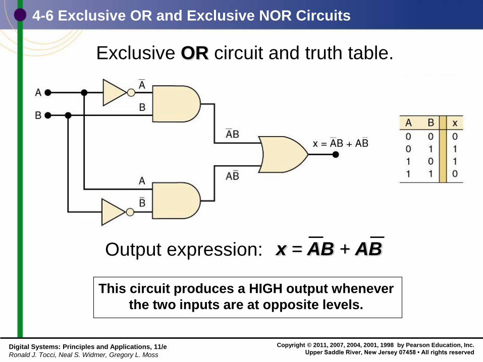
4-6 Exclusive OR and Exclusive NOR Circuits
Exclusive OR circuit and truth table.
x = AB + AB Output expression:
This circuit produces a HIGH output whenever
the two inputs are at opposite levels.
Copyright © 2011, 2007, 2004, 2001, 1998 by Pearson Education, Inc.
Upper Saddle River, New Jersey 07458 • All rights reserved Digital Systems: Principles and Applications, 11/e
Ronald J. Tocci, Neal S. Widmer, Gregory L. Moss
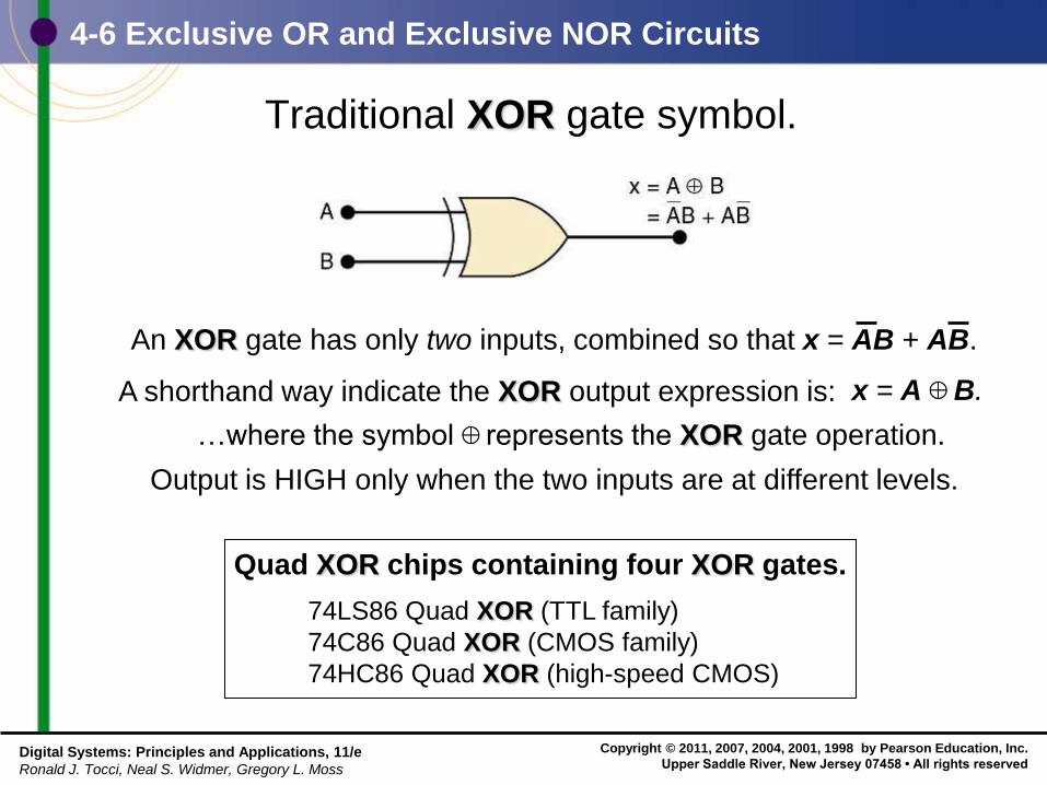
4-6 Exclusive OR and Exclusive NOR Circuits
Traditional XOR gate symbol.
x = A B. A shorthand way indicate the XOR output expression is:
…where the symbol represents the XOR gate operation.
An XOR gate has only two inputs, combined so that x = AB + AB.
Output is HIGH only when the two inputs are at different levels.
74LS86 Quad XOR (TTL family)
74C86 Quad XOR (CMOS family)
74HC86 Quad XOR (high-speed CMOS)
Quad XOR chips containing four XOR gates.
Copyright © 2011, 2007, 2004, 2001, 1998 by Pearson Education, Inc.
Upper Saddle River, New Jersey 07458 • All rights reserved Digital Systems: Principles and Applications, 11/e
Ronald J. Tocci, Neal S. Widmer, Gregory L. Moss
4-6 Exclusive OR and Exclusive NOR Circuits
• The exclusive NOR (XNOR) produces a HIGH
output whenever the two inputs are at the
same level.
– XOR and XNOR outputs are opposite.
Copyright © 2011, 2007, 2004, 2001, 1998 by Pearson Education, Inc.
Upper Saddle River, New Jersey 07458 • All rights reserved Digital Systems: Principles and Applications, 11/e
Ronald J. Tocci, Neal S. Widmer, Gregory L. Moss
4-6 Exclusive OR and Exclusive NOR Circuits
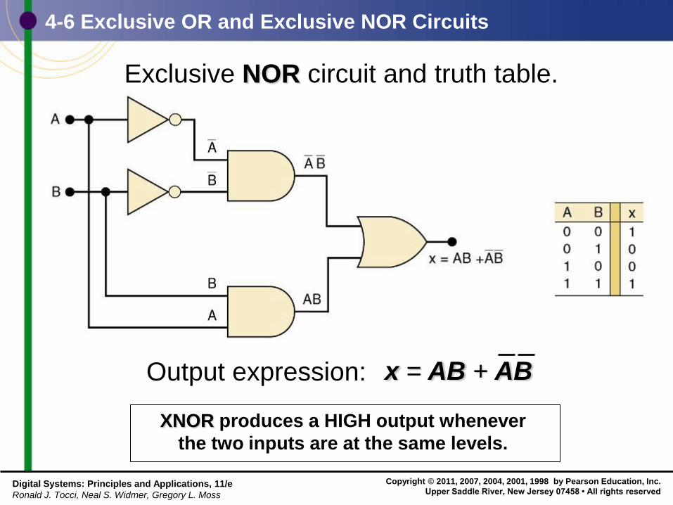
Exclusive NOR circuit and truth table.
x = AB + AB Output expression:
XNOR produces a HIGH output whenever
the two inputs are at the same levels.
Copyright © 2011, 2007, 2004, 2001, 1998 by Pearson Education, Inc.
Upper Saddle River, New Jersey 07458 • All rights reserved Digital Systems: Principles and Applications, 11/e
Ronald J. Tocci, Neal S. Widmer, Gregory L. Moss
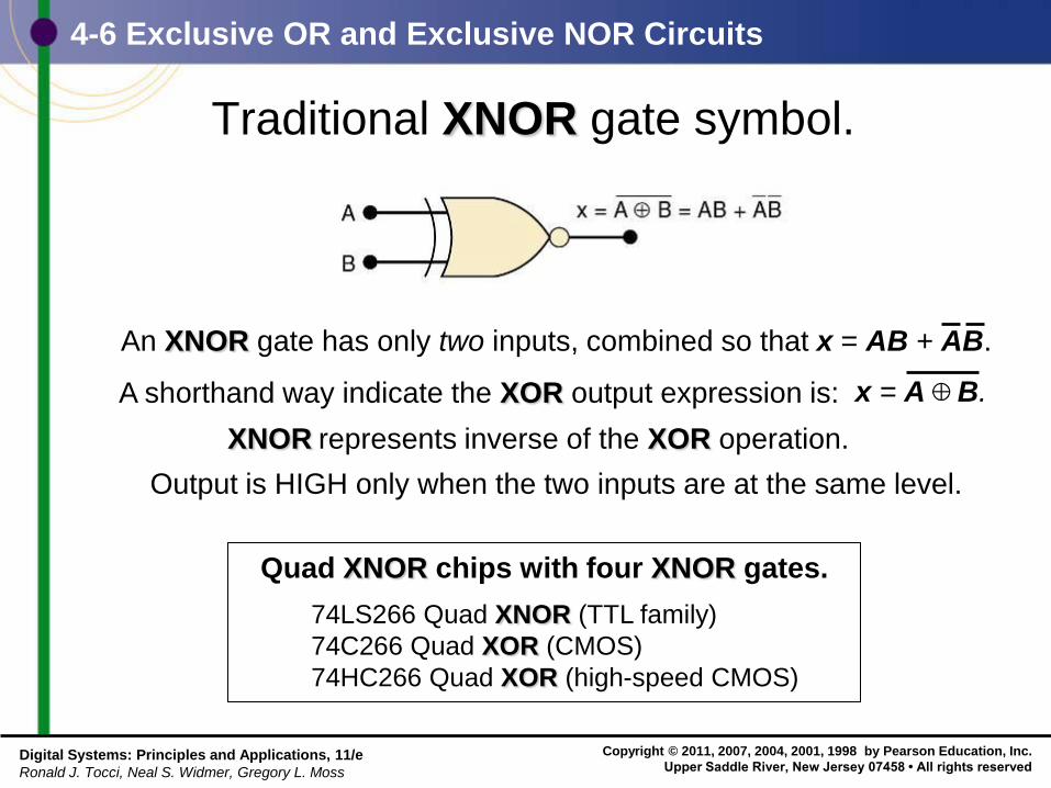
4-6 Exclusive OR and Exclusive NOR Circuits
Traditional XNOR gate symbol.
74LS266 Quad XNOR (TTL family)
74C266 Quad XOR (CMOS)
74HC266 Quad XOR (high-speed CMOS)
Quad XNOR chips with four XNOR gates.
Output is HIGH only when the two inputs are at the same level.
XNOR represents inverse of the XOR operation.
x = A B. A shorthand way indicate the XOR output expression is:
An XNOR gate has only two inputs, combined so that x = AB + AB.
Copyright © 2011, 2007, 2004, 2001, 1998 by Pearson Education, Inc.
Upper Saddle River, New Jersey 07458 • All rights reserved Digital Systems: Principles and Applications, 11/e
Ronald J. Tocci, Neal S. Widmer, Gregory L. Moss
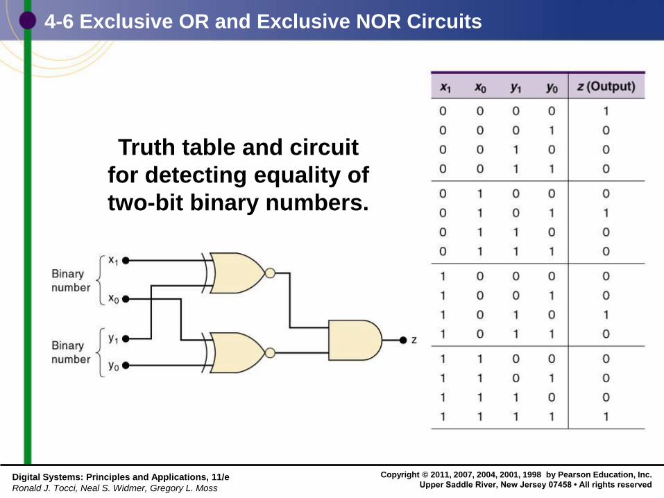
4-6 Exclusive OR and Exclusive NOR Circuits
Truth table and circuit
for detecting equality of
two-bit binary numbers.
Copyright © 2011, 2007, 2004, 2001, 1998 by Pearson Education, Inc.
Upper Saddle River, New Jersey 07458 • All rights reserved Digital Systems: Principles and Applications, 11/e
Ronald J. Tocci, Neal S. Widmer, Gregory L. Moss
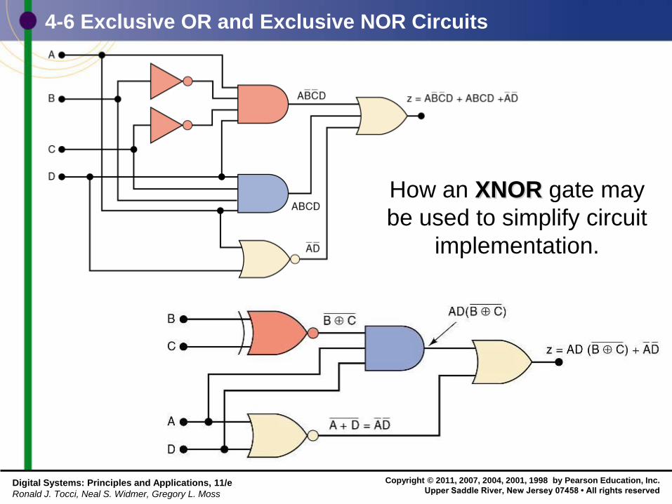
4-6 Exclusive OR and Exclusive NOR Circuits
How an XNOR gate may
be used to simplify circuit
implementation.
Copyright © 2011, 2007, 2004, 2001, 1998 by Pearson Education, Inc.
Upper Saddle River, New Jersey 07458 • All rights reserved Digital Systems: Principles and Applications, 11/e
Ronald J. Tocci, Neal S. Widmer, Gregory L. Moss
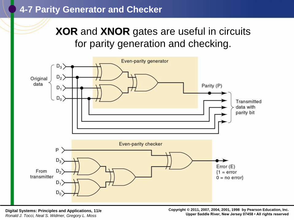
4-7 Parity Generator and Checker
XOR and XNOR gates are useful in circuits
for parity generation and checking.
Copyright © 2011, 2007, 2004, 2001, 1998 by Pearson Education, Inc.
Upper Saddle River, New Jersey 07458 • All rights reserved Digital Systems: Principles and Applications, 11/e
Ronald J. Tocci, Neal S. Widmer, Gregory L. Moss
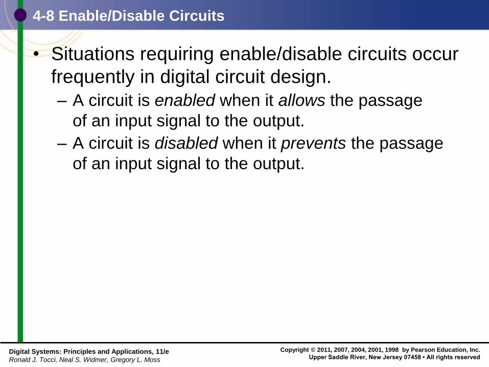
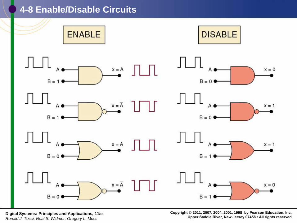
4-8 Enable/Disable Circuits
• Situations requiring enable/disable circuits occur
frequently in digital circuit design.
– A circuit is enabled when it allows the passage
of an input signal to the output.
– A circuit is disabled when it prevents the passage
of an input signal to the output.
Copyright © 2011, 2007, 2004, 2001, 1998 by Pearson Education, Inc.
Upper Saddle River, New Jersey 07458 • All rights reserved Digital Systems: Principles and Applications, 11/e
Ronald J. Tocci, Neal S. Widmer, Gregory L. Moss
4-8 Enable/Disable Circuits
Copyright © 2011, 2007, 2004, 2001, 1998 by Pearson Education, Inc.
Upper Saddle River, New Jersey 07458 • All rights reserved Digital Systems: Principles and Applications, 11/e
Ronald J. Tocci, Neal S. Widmer, Gregory L. Moss
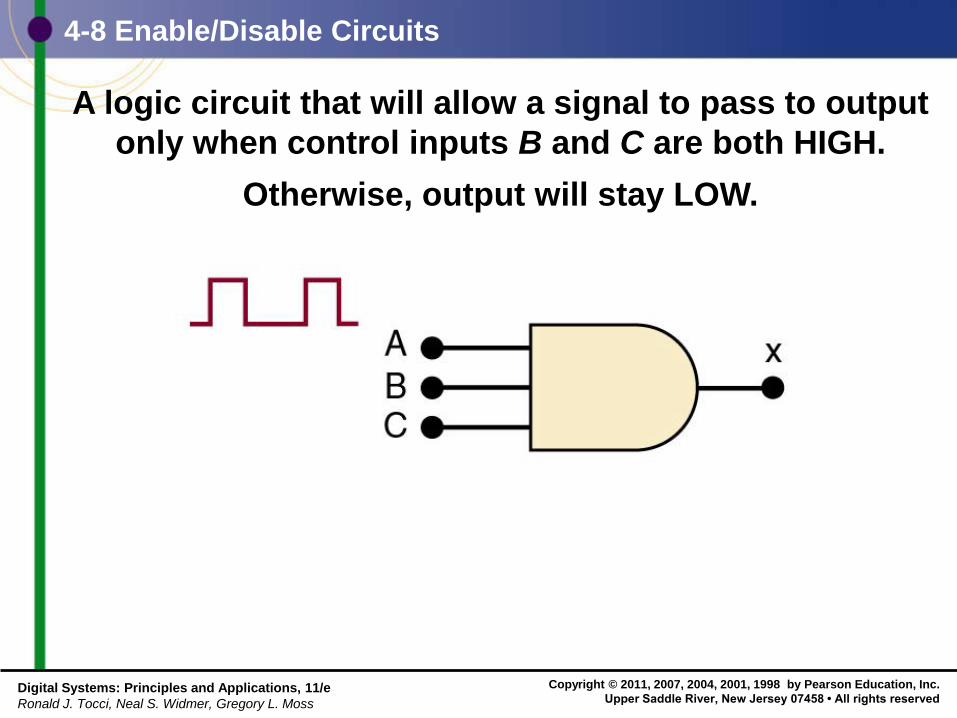
4-8 Enable/Disable Circuits
A logic circuit that will allow a signal to pass to output
only when control inputs B and C are both HIGH.
Otherwise, output will stay LOW.
Copyright © 2011, 2007, 2004, 2001, 1998 by Pearson Education, Inc.
Upper Saddle River, New Jersey 07458 • All rights reserved Digital Systems: Principles and Applications, 11/e
Ronald J. Tocci, Neal S. Widmer, Gregory L. Moss
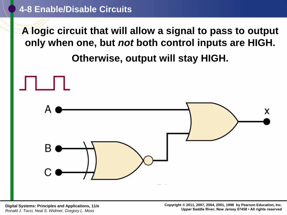
4-8 Enable/Disable Circuits
A logic circuit that will allow a signal to pass to output
only when one, but not both control inputs are HIGH.
Otherwise, output will stay HIGH.
Copyright © 2011, 2007, 2004, 2001, 1998 by Pearson Education, Inc.
Upper Saddle River, New Jersey 07458 • All rights reserved Digital Systems: Principles and Applications, 11/e
Ronald J. Tocci, Neal S. Widmer, Gregory L. Moss
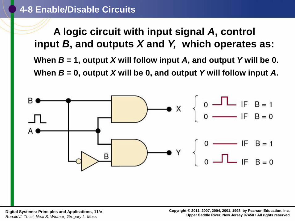
4-8 Enable/Disable Circuits
A logic circuit with input signal A, control
input B, and outputs X and Y, which operates as:
When B = 1, output X will follow input A, and output Y will be 0.
When B = 0, output X will be 0, and output Y will follow input A.
Copyright © 2011, 2007, 2004, 2001, 1998 by Pearson Education, Inc.
Upper Saddle River, New Jersey 07458 • All rights reserved Digital Systems: Principles and Applications, 11/e
Ronald J. Tocci, Neal S. Widmer, Gregory L. Moss
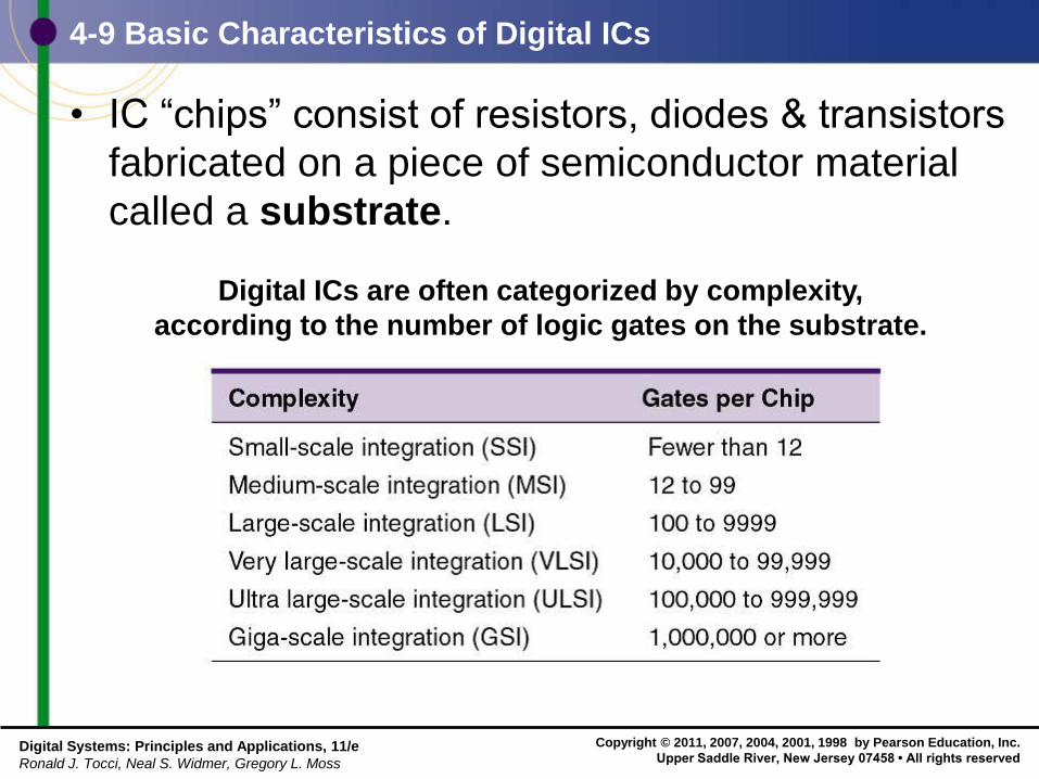
4-9 Basic Characteristics of Digital ICs
• IC “chips” consist of resistors, diodes & transistors
fabricated on a piece of semiconductor material
called a substrate.
Digital ICs are often categorized by complexity,
according to the number of logic gates on the substrate.
Copyright © 2011, 2007, 2004, 2001, 1998 by Pearson Education, Inc.
Upper Saddle River, New Jersey 07458 • All rights reserved Digital Systems: Principles and Applications, 11/e
Ronald J. Tocci, Neal S. Widmer, Gregory L. Moss
4-9 Basic Characteristics of Digital ICs
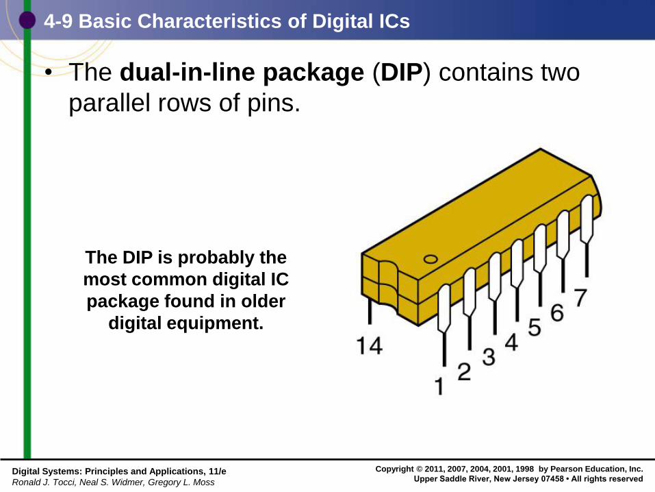
• The dual-in-line package (DIP) contains two
parallel rows of pins.
The DIP is probably the
most common digital IC
package found in older
digital equipment.
Copyright © 2011, 2007, 2004, 2001, 1998 by Pearson Education, Inc.
Upper Saddle River, New Jersey 07458 • All rights reserved Digital Systems: Principles and Applications, 11/e
Ronald J. Tocci, Neal S. Widmer, Gregory L. Moss
4-9 Basic Characteristics of Digital ICs
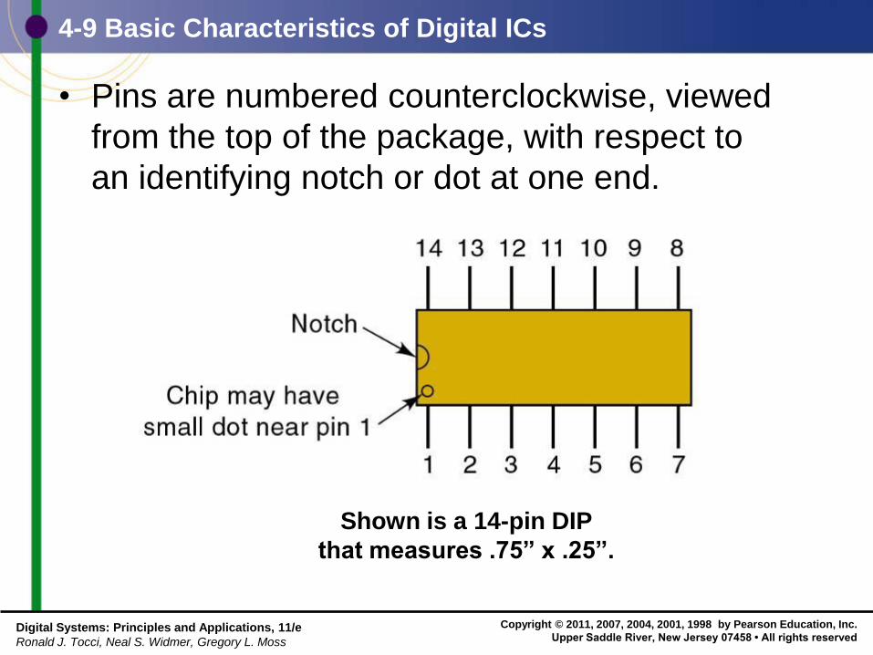
• Pins are numbered counterclockwise, viewed
from the top of the package, with respect to
an identifying notch or dot at one end.
Shown is a 14-pin DIP
that measures .75” x .25”.
Copyright © 2011, 2007, 2004, 2001, 1998 by Pearson Education, Inc.
Upper Saddle River, New Jersey 07458 • All rights reserved Digital Systems: Principles and Applications, 11/e
Ronald J. Tocci, Neal S. Widmer, Gregory L. Moss
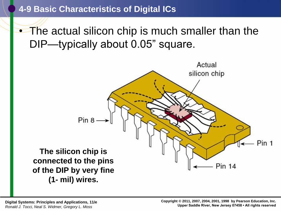
4-9 Basic Characteristics of Digital ICs
• The actual silicon chip is much smaller than the
DIP—typically about 0.05” square.
The silicon chip is
connected to the pins
of the DIP by very fine
(1- mil) wires.
Copyright © 2011, 2007, 2004, 2001, 1998 by Pearson Education, Inc.
Upper Saddle River, New Jersey 07458 • All rights reserved Digital Systems: Principles and Applications, 11/e
Ronald J. Tocci, Neal S. Widmer, Gregory L. Moss
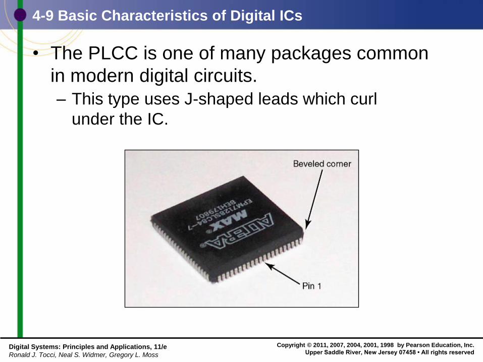
4-9 Basic Characteristics of Digital ICs
• The PLCC is one of many packages common
in modern digital circuits.
– This type uses J-shaped leads which curl
under the IC.
Copyright © 2011, 2007, 2004, 2001, 1998 by Pearson Education, Inc.
Upper Saddle River, New Jersey 07458 • All rights reserved Digital Systems: Principles and Applications, 11/e
Ronald J. Tocci, Neal S. Widmer, Gregory L. Moss
4-9 Basic Characteristics of Digital ICs
• ICs are also categorized by the type of
components used in their circuits.
– Bipolar ICs use NPN and PNP transistors
– Unipolar ICs use FET transistors.
Copyright © 2011, 2007, 2004, 2001, 1998 by Pearson Education, Inc.
Upper Saddle River, New Jersey 07458 • All rights reserved Digital Systems: Principles and Applications, 11/e
Ronald J. Tocci, Neal S. Widmer, Gregory L. Moss
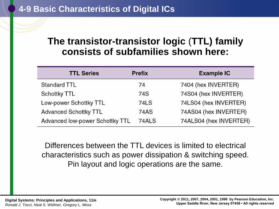
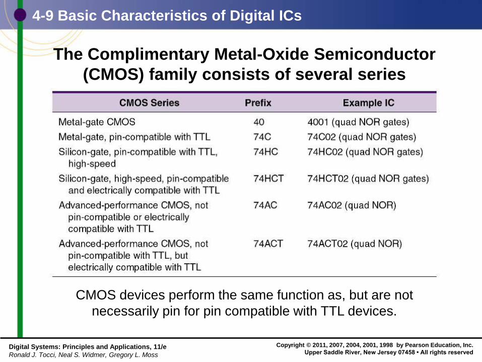
4-9 Basic Characteristics of Digital ICs
The transistor-transistor logic (TTL) family consists of subfamilies shown here:
Differences between the TTL devices is limited to electrical
characteristics such as power dissipation & switching speed.
Pin layout and logic operations are the same.
Copyright © 2011, 2007, 2004, 2001, 1998 by Pearson Education, Inc.
Upper Saddle River, New Jersey 07458 • All rights reserved Digital Systems: Principles and Applications, 11/e
Ronald J. Tocci, Neal S. Widmer, Gregory L. Moss
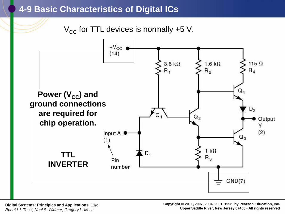
4-9 Basic Characteristics of Digital ICs
TTL
INVERTER
Power (VCC) and
ground connections
are required for
chip operation.
VCC for TTL devices is normally +5 V.
Copyright © 2011, 2007, 2004, 2001, 1998 by Pearson Education, Inc.
Upper Saddle River, New Jersey 07458 • All rights reserved Digital Systems: Principles and Applications, 11/e
Ronald J. Tocci, Neal S. Widmer, Gregory L. Moss
4-9 Basic Characteristics of Digital ICs
The Complimentary Metal-Oxide Semiconductor
(CMOS) family consists of several series
CMOS devices perform the same function as, but are not
necessarily pin for pin compatible with TTL devices.
Copyright © 2011, 2007, 2004, 2001, 1998 by Pearson Education, Inc.
Upper Saddle River, New Jersey 07458 • All rights reserved Digital Systems: Principles and Applications, 11/e
Ronald J. Tocci, Neal S. Widmer, Gregory L. Moss
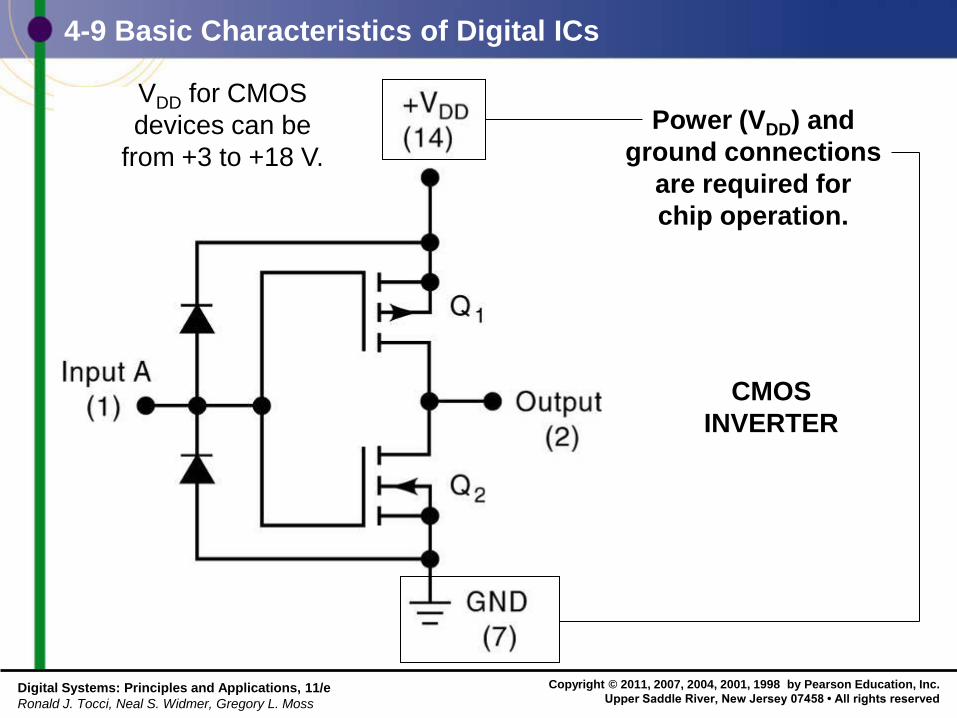
Power (VDD) and
ground connections
are required for
chip operation.
4-9 Basic Characteristics of Digital ICs
CMOS
INVERTER
VDD for CMOS
devices can be
from +3 to +18 V.
Copyright © 2011, 2007, 2004, 2001, 1998 by Pearson Education, Inc.
Upper Saddle River, New Jersey 07458 • All rights reserved Digital Systems: Principles and Applications, 11/e
Ronald J. Tocci, Neal S. Widmer, Gregory L. Moss
4-9 Basic Characteristics of Digital ICs
• Inputs not connected are said to be floating.
– Floating TTL input acts like a logic 1.
• Voltage measurement may appear indeterminate,
but the device behaves as if there is a 1 on the
floating input
– Floating CMOS inputs can cause overheating and
damage to the device.
• Some ICs have protection circuits built in.
– The best practice is to tie all unused inputs.
• Either high or low.
Copyright © 2011, 2007, 2004, 2001, 1998 by Pearson Education, Inc.
Upper Saddle River, New Jersey 07458 • All rights reserved Digital Systems: Principles and Applications, 11/e
Ronald J. Tocci, Neal S. Widmer, Gregory L. Moss
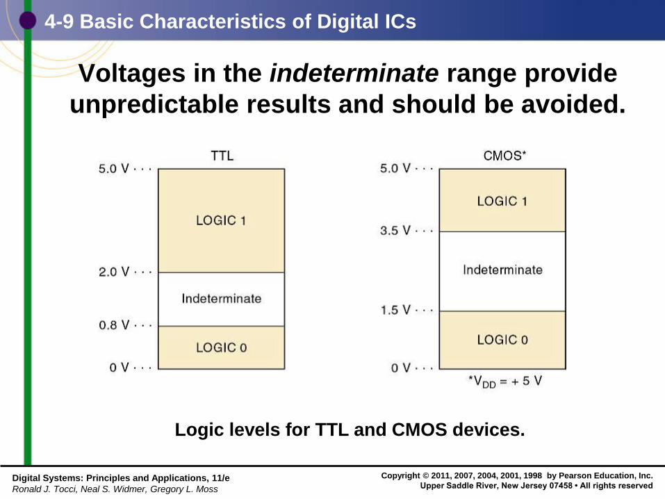
4-9 Basic Characteristics of Digital ICs
Voltages in the indeterminate range provide
unpredictable results and should be avoided.
Logic levels for TTL and CMOS devices.
Copyright © 2011, 2007, 2004, 2001, 1998 by Pearson Education, Inc.
Upper Saddle River, New Jersey 07458 • All rights reserved Digital Systems: Principles and Applications, 11/e
Ronald J. Tocci, Neal S. Widmer, Gregory L. Moss
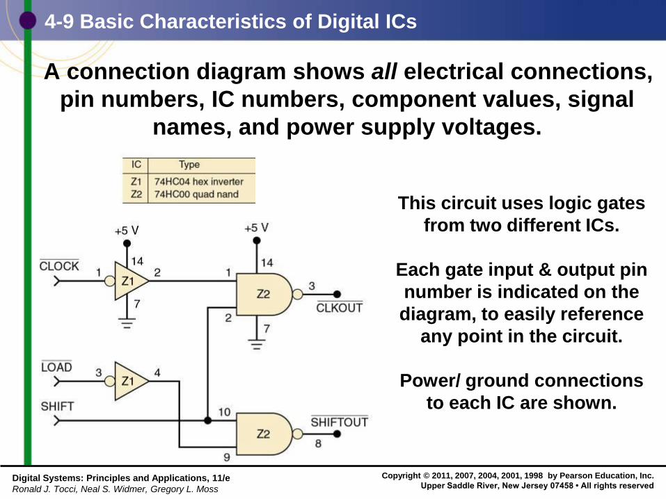
4-9 Basic Characteristics of Digital ICs
A connection diagram shows all electrical connections,
pin numbers, IC numbers, component values, signal
names, and power supply voltages.
This circuit uses logic gates
from two different ICs.
Each gate input & output pin
number is indicated on the
diagram, to easily reference
any point in the circuit.
Power/ ground connections
to each IC are shown.
Copyright © 2011, 2007, 2004, 2001, 1998 by Pearson Education, Inc.
Upper Saddle River, New Jersey 07458 • All rights reserved Digital Systems: Principles and Applications, 11/e
Ronald J. Tocci, Neal S. Widmer, Gregory L. Moss
4-9 Basic Characteristics of Digital ICs
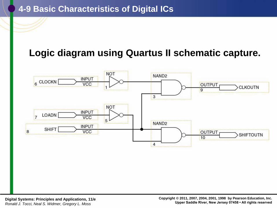
Logic diagram using Quartus II schematic capture.
Copyright © 2011, 2007, 2004, 2001, 1998 by Pearson Education, Inc.
Upper Saddle River, New Jersey 07458 • All rights reserved Digital Systems: Principles and Applications, 11/e
Ronald J. Tocci, Neal S. Widmer, Gregory L. Moss
4-10 Troubleshooting Digital Systems
• Three basic steps in fixing a digital circuit or
system that has a fault (failure):
– Fault detection—determine operation to expected
operation.
– Fault isolation—test & measure to isolate the fault.
– Fault correction—repair the fault.
• The basic troubleshooting tools are the logic probe,
oscilloscope, and logic pulser.
Copyright © 2011, 2007, 2004, 2001, 1998 by Pearson Education, Inc.
Upper Saddle River, New Jersey 07458 • All rights reserved Digital Systems: Principles and Applications, 11/e
Ronald J. Tocci, Neal S. Widmer, Gregory L. Moss
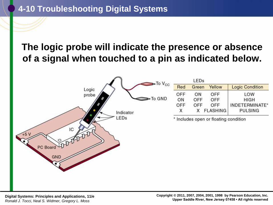
4-10 Troubleshooting Digital Systems
The logic probe will indicate the presence or absence
of a signal when touched to a pin as indicated below.
Copyright © 2011, 2007, 2004, 2001, 1998 by Pearson Education, Inc.
Upper Saddle River, New Jersey 07458 • All rights reserved Digital Systems: Principles and Applications, 11/e
Ronald J. Tocci, Neal S. Widmer, Gregory L. Moss
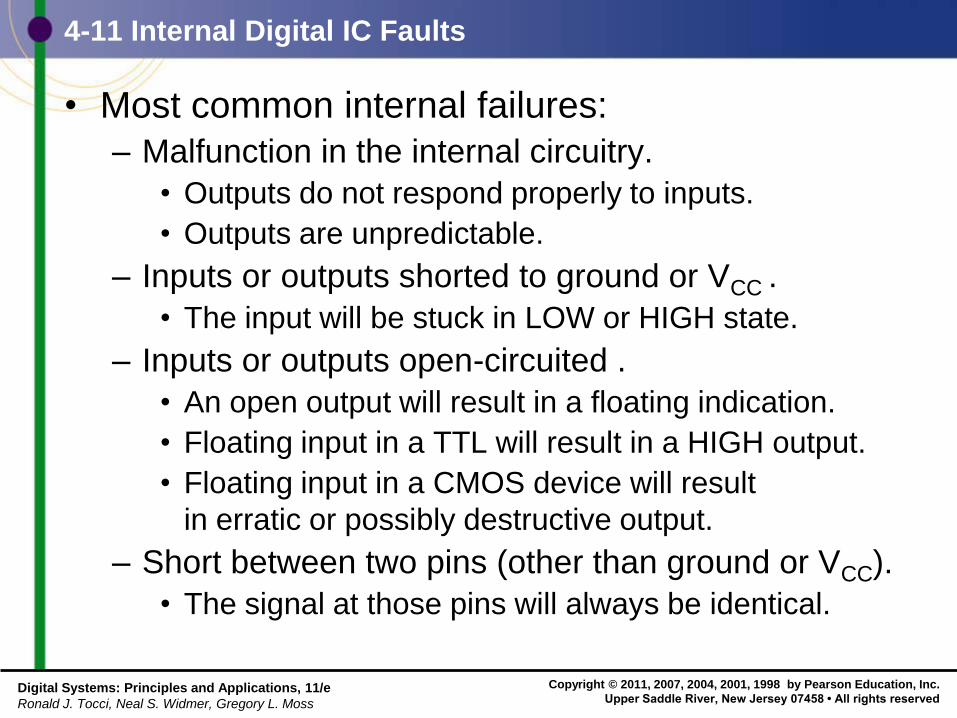
4-11 Internal Digital IC Faults
• Most common internal failures:
– Malfunction in the internal circuitry.
• Outputs do not respond properly to inputs.
• Outputs are unpredictable.
– Inputs or outputs shorted to ground or VCC .
• The input will be stuck in LOW or HIGH state.
– Inputs or outputs open-circuited .
• An open output will result in a floating indication.
• Floating input in a TTL will result in a HIGH output.
• Floating input in a CMOS device will result
in erratic or possibly destructive output.
– Short between two pins (other than ground or VCC).
• The signal at those pins will always be identical.
Copyright © 2011, 2007, 2004, 2001, 1998 by Pearson Education, Inc.
Upper Saddle River, New Jersey 07458 • All rights reserved Digital Systems: Principles and Applications, 11/e
Ronald J. Tocci, Neal S. Widmer, Gregory L. Moss
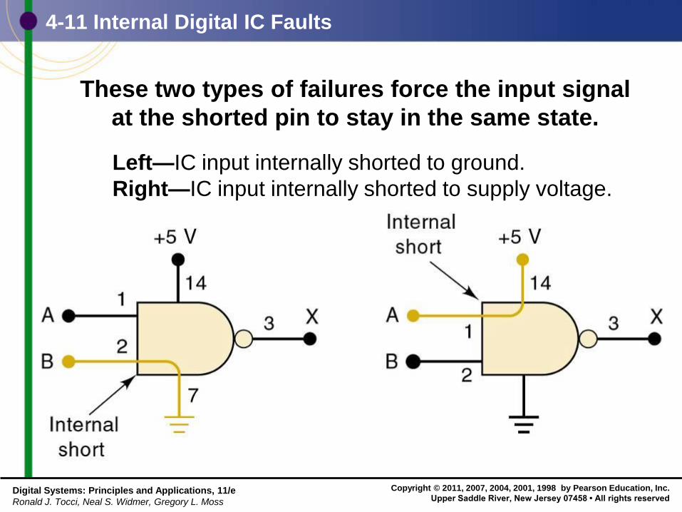
4-11 Internal Digital IC Faults
These two types of failures force the input signal
at the shorted pin to stay in the same state.
Left—IC input internally shorted to ground.
Right—IC input internally shorted to supply voltage.
Copyright © 2011, 2007, 2004, 2001, 1998 by Pearson Education, Inc.
Upper Saddle River, New Jersey 07458 • All rights reserved Digital Systems: Principles and Applications, 11/e
Ronald J. Tocci, Neal S. Widmer, Gregory L. Moss
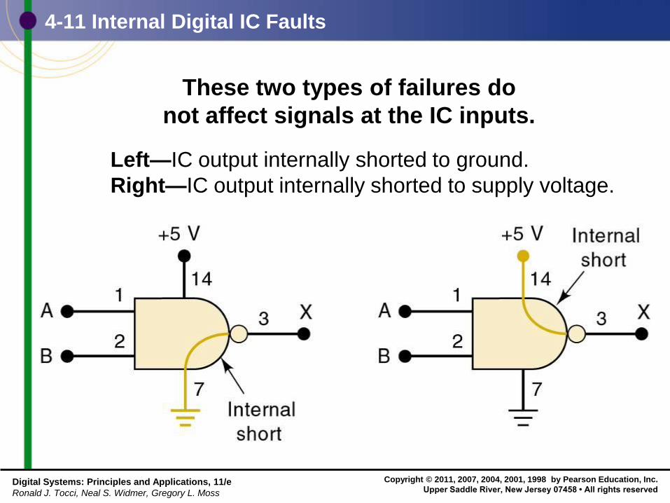
4-11 Internal Digital IC Faults
These two types of failures do
not affect signals at the IC inputs.
Left—IC output internally shorted to ground.
Right—IC output internally shorted to supply voltage.
Copyright © 2011, 2007, 2004, 2001, 1998 by Pearson Education, Inc.
Upper Saddle River, New Jersey 07458 • All rights reserved Digital Systems: Principles and Applications, 11/e
Ronald J. Tocci, Neal S. Widmer, Gregory L. Moss
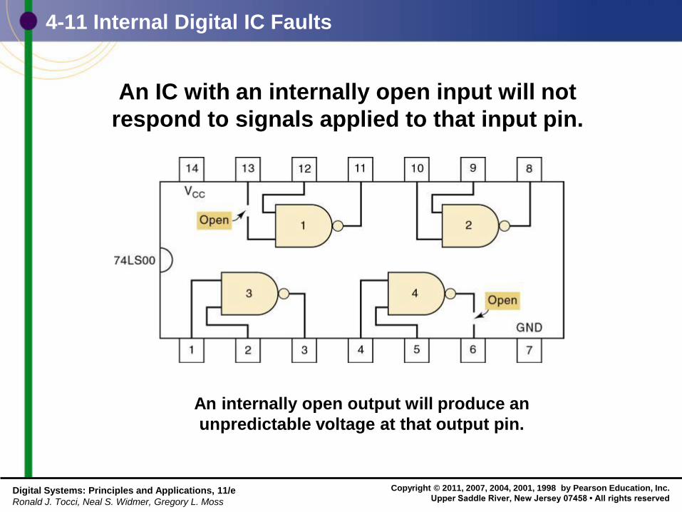
4-11 Internal Digital IC Faults
An IC with an internally open input will not
respond to signals applied to that input pin.
An internally open output will produce an
unpredictable voltage at that output pin.
Copyright © 2011, 2007, 2004, 2001, 1998 by Pearson Education, Inc.
Upper Saddle River, New Jersey 07458 • All rights reserved Digital Systems: Principles and Applications, 11/e
Ronald J. Tocci, Neal S. Widmer, Gregory L. Moss
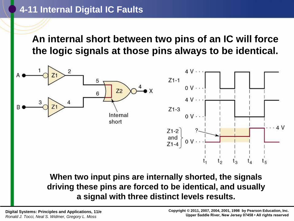
4-11 Internal Digital IC Faults
An internal short between two pins of an IC will force
the logic signals at those pins always to be identical.
When two input pins are internally shorted, the signals
driving these pins are forced to be identical, and usually
a signal with three distinct levels results.
Copyright © 2011, 2007, 2004, 2001, 1998 by Pearson Education, Inc.
Upper Saddle River, New Jersey 07458 • All rights reserved Digital Systems: Principles and Applications, 11/e
Ronald J. Tocci, Neal S. Widmer, Gregory L. Moss
4-12 External Faults
• Open signal lines—signal prevented from moving
between points—can be caused by:
– Broken wire.
– Poor connections (solder or wire-wrap).
– Cut or crack on PC board trace.
– Bent or broken IC pins.
– Faulty IC socket.
• This type of fault can be detected visually and
verified with an ohmmeter between the points
in question.
Copyright © 2011, 2007, 2004, 2001, 1998 by Pearson Education, Inc.
Upper Saddle River, New Jersey 07458 • All rights reserved Digital Systems: Principles and Applications, 11/e
Ronald J. Tocci, Neal S. Widmer, Gregory L. Moss
4-12 External Faults
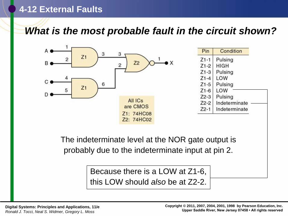
What is the most probable fault in the circuit shown?
The indeterminate level at the NOR gate output is
probably due to the indeterminate input at pin 2.
Because there is a LOW at Z1-6,
this LOW should also be at Z2-2.
Copyright © 2011, 2007, 2004, 2001, 1998 by Pearson Education, Inc.
Upper Saddle River, New Jersey 07458 • All rights reserved Digital Systems: Principles and Applications, 11/e
Ronald J. Tocci, Neal S. Widmer, Gregory L. Moss
4-12 External Faults
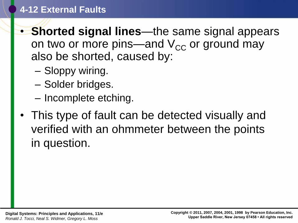
• Shorted signal lines—the same signal appears on two or more pins—and VCC or ground may also be shorted, caused by:
– Sloppy wiring.
– Solder bridges.
– Incomplete etching.
• This type of fault can be detected visually and
verified with an ohmmeter between the points
in question.
Copyright © 2011, 2007, 2004, 2001, 1998 by Pearson Education, Inc.
Upper Saddle River, New Jersey 07458 • All rights reserved Digital Systems: Principles and Applications, 11/e
Ronald J. Tocci, Neal S. Widmer, Gregory L. Moss
4-12 External Faults
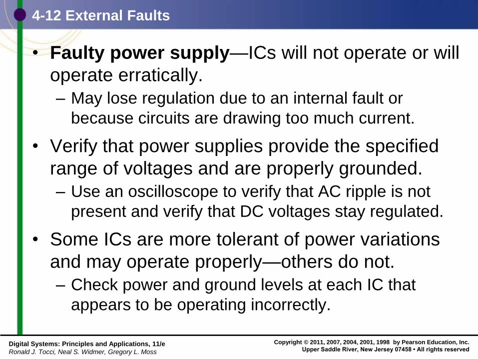
• Faulty power supply—ICs will not operate or will
operate erratically.
– May lose regulation due to an internal fault or
because circuits are drawing too much current.
• Verify that power supplies provide the specified
range of voltages and are properly grounded.
– Use an oscilloscope to verify that AC ripple is not
present and verify that DC voltages stay regulated.
• Some ICs are more tolerant of power variations
and may operate properly—others do not.
– Check power and ground levels at each IC that
appears to be operating incorrectly.
Copyright © 2011, 2007, 2004, 2001, 1998 by Pearson Education, Inc.
Upper Saddle River, New Jersey 07458 • All rights reserved Digital Systems: Principles and Applications, 11/e
Ronald J. Tocci, Neal S. Widmer, Gregory L. Moss
4-12 External Faults
• Output loading—caused by connecting too many
inputs to the output of an IC, exceeding output
current rating.
– Output voltage falls into the indeterminate range.
• Called loading the output signal.
– Usually a result of poor design or bad connection.
Copyright © 2011, 2007, 2004, 2001, 1998 by Pearson Education, Inc.
Upper Saddle River, New Jersey 07458 • All rights reserved Digital Systems: Principles and Applications, 11/e
Ronald J. Tocci, Neal S. Widmer, Gregory L. Moss
4-14 Programmable Logic Devices
• The concept behind programmable logic devices
is simple—lots of logic gates in a single IC.
– Control of the interconnection of these gates
electronically.
• PLDs allow the design process to be automated.
– Designers identify inputs, outputs, and logical
relationships.
• PLDs are electronically configured to form the
defined logic circuits.
Copyright © 2011, 2007, 2004, 2001, 1998 by Pearson Education, Inc.
Upper Saddle River, New Jersey 07458 • All rights reserved Digital Systems: Principles and Applications, 11/e
Ronald J. Tocci, Neal S. Widmer, Gregory L. Moss
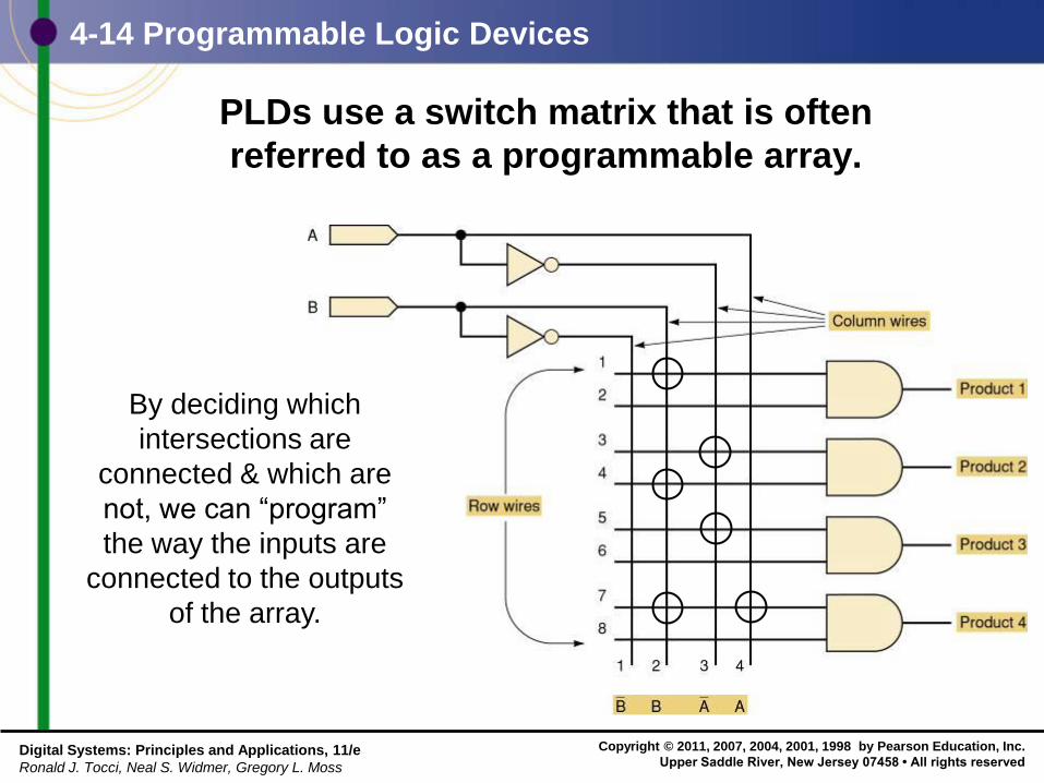
4-14 Programmable Logic Devices
PLDs use a switch matrix that is often
referred to as a programmable array.
By deciding which
intersections are
connected & which are
not, we can “program”
the way the inputs are
connected to the outputs
of the array.
Copyright © 2011, 2007, 2004, 2001, 1998 by Pearson Education, Inc.
Upper Saddle River, New Jersey 07458 • All rights reserved Digital Systems: Principles and Applications, 11/e
Ronald J. Tocci, Neal S. Widmer, Gregory L. Moss
4-14 Programmable Logic Devices
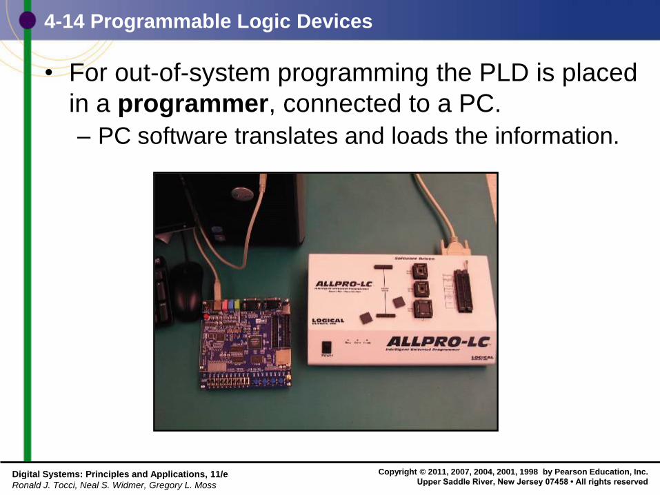
• For out-of-system programming the PLD is placed
in a programmer, connected to a PC.
– PC software translates and loads the information.
Copyright © 2011, 2007, 2004, 2001, 1998 by Pearson Education, Inc.
Upper Saddle River, New Jersey 07458 • All rights reserved Digital Systems: Principles and Applications, 11/e
Ronald J. Tocci, Neal S. Widmer, Gregory L. Moss
4-14 Programmable Logic Devices
• In-system programming is done by connecting
directly to “portal” pins while the IC remains in
the system. – An interface cable connects the PLD to a PC
running the software that loads the device.
Copyright © 2011, 2007, 2004, 2001, 1998 by Pearson Education, Inc.
Upper Saddle River, New Jersey 07458 • All rights reserved Digital Systems: Principles and Applications, 11/e
Ronald J. Tocci, Neal S. Widmer, Gregory L. Moss
4-14 Programmable Logic Devices
• Logic circuits can be described using schematic
diagrams, logic equations, truth tables, and HDL.
– PLD development software can convert any of these
descriptions into 1s and 0s and loaded into the PLD.
• Altera MAX+PLUS II is a development software
that allows the user to describe circuits using
graphic design files and timing diagrams.
Copyright © 2011, 2007, 2004, 2001, 1998 by Pearson Education, Inc.
Upper Saddle River, New Jersey 07458 • All rights reserved Digital Systems: Principles and Applications, 11/e
Ronald J. Tocci, Neal S. Widmer, Gregory L. Moss
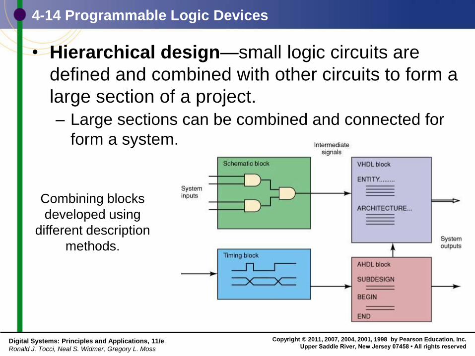
Combining blocks
developed using
different description
methods.
4-14 Programmable Logic Devices
• Hierarchical design—small logic circuits are
defined and combined with other circuits to form a
large section of a project.
– Large sections can be combined and connected for
form a system.
Copyright © 2011, 2007, 2004, 2001, 1998 by Pearson Education, Inc.
Upper Saddle River, New Jersey 07458 • All rights reserved Digital Systems: Principles and Applications, 11/e
Ronald J. Tocci, Neal S. Widmer, Gregory L. Moss
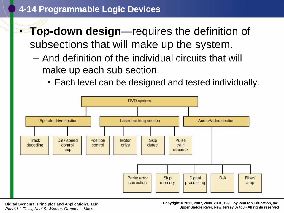
4-14 Programmable Logic Devices
• Top-down design—requires the definition of
subsections that will make up the system.
– And definition of the individual circuits that will
make up each sub section.
• Each level can be designed and tested individually.
Copyright © 2011, 2007, 2004, 2001, 1998 by Pearson Education, Inc.
Upper Saddle River, New Jersey 07458 • All rights reserved Digital Systems: Principles and Applications, 11/e
Ronald J. Tocci, Neal S. Widmer, Gregory L. Moss
4-14 Programmable Logic Devices
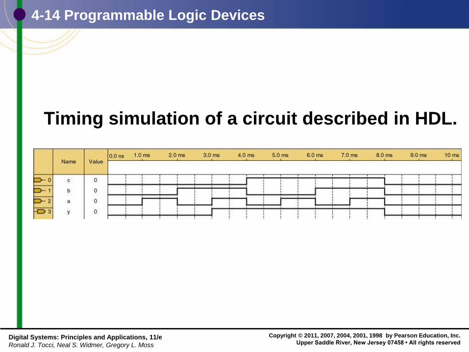
Timing simulation of a circuit described in HDL.
Copyright © 2011, 2007, 2004, 2001, 1998 by Pearson Education, Inc.
Upper Saddle River, New Jersey 07458 • All rights reserved Digital Systems: Principles and Applications, 11/e
Ronald J. Tocci, Neal S. Widmer, Gregory L. Moss
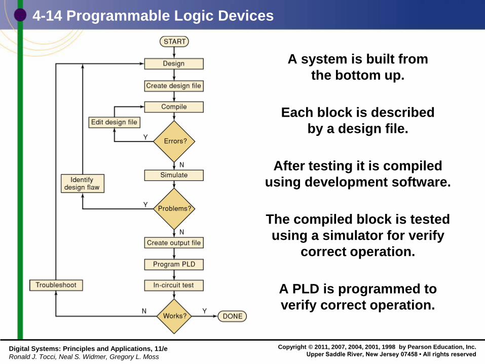
4-14 Programmable Logic Devices
A system is built from
the bottom up.
Each block is described
by a design file.
After testing it is compiled
using development software.
The compiled block is tested
using a simulator for verify
correct operation.
A PLD is programmed to
verify correct operation.
Copyright © 2011, 2007, 2004, 2001, 1998 by Pearson Education, Inc.
Upper Saddle River, New Jersey 07458 • All rights reserved Digital Systems: Principles and Applications, 11/e
Ronald J. Tocci, Neal S. Widmer, Gregory L. Moss
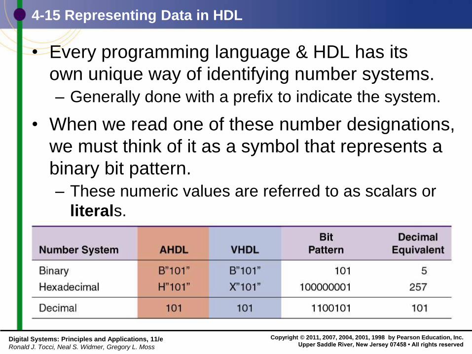
4-15 Representing Data in HDL
• Every programming language & HDL has its
own unique way of identifying number systems.
– Generally done with a prefix to indicate the system.
• When we read one of these number designations,
we must think of it as a symbol that represents a
binary bit pattern.
– These numeric values are referred to as scalars or
literals.
Copyright © 2011, 2007, 2004, 2001, 1998 by Pearson Education, Inc.
Upper Saddle River, New Jersey 07458 • All rights reserved Digital Systems: Principles and Applications, 11/e
Ronald J. Tocci, Neal S. Widmer, Gregory L. Moss
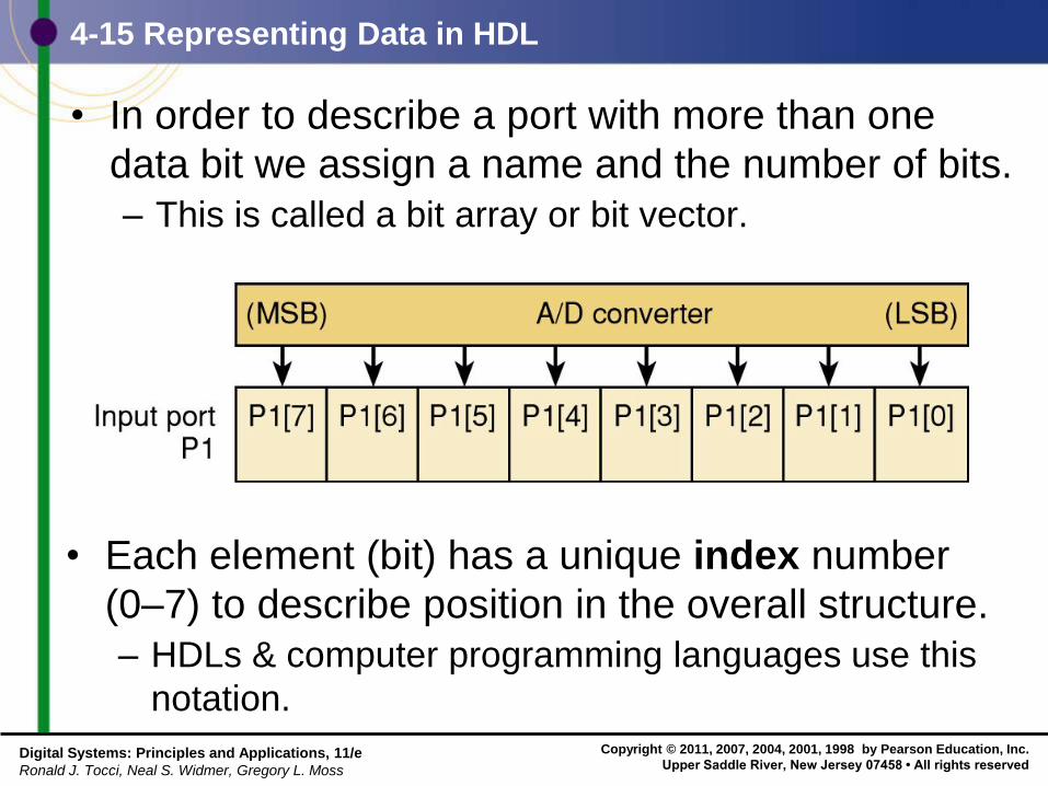
4-15 Representing Data in HDL
• In order to describe a port with more than one
data bit we assign a name and the number of bits.
– This is called a bit array or bit vector.
• Each element (bit) has a unique index number
(0–7) to describe position in the overall structure.
– HDLs & computer programming languages use this
notation.
Copyright © 2011, 2007, 2004, 2001, 1998 by Pearson Education, Inc.
Upper Saddle River, New Jersey 07458 • All rights reserved Digital Systems: Principles and Applications, 11/e
Ronald J. Tocci, Neal S. Widmer, Gregory L. Moss
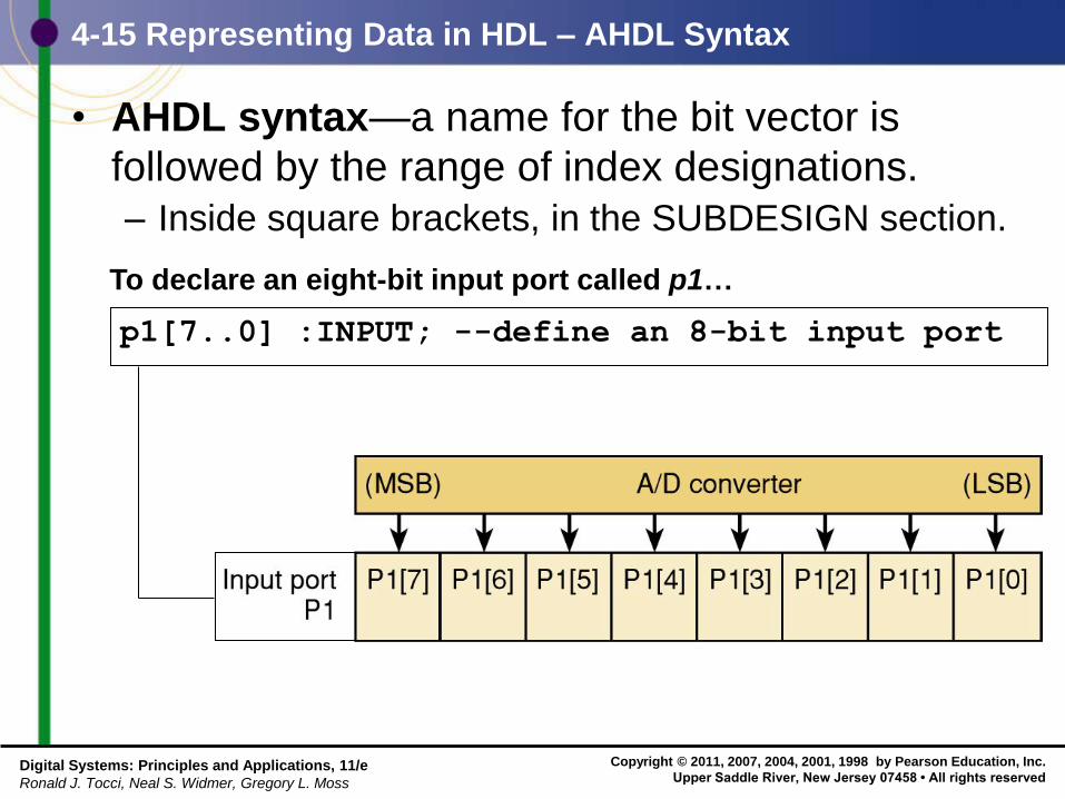
4-15 Representing Data in HDL – AHDL Syntax
• AHDL syntax—a name for the bit vector is
followed by the range of index designations.
– Inside square brackets, in the SUBDESIGN section.
p1[7..0] :INPUT; --define an 8-bit input port
To declare an eight-bit input port called p1…
Copyright © 2011, 2007, 2004, 2001, 1998 by Pearson Education, Inc.
Upper Saddle River, New Jersey 07458 • All rights reserved Digital Systems: Principles and Applications, 11/e
Ronald J. Tocci, Neal S. Widmer, Gregory L. Moss
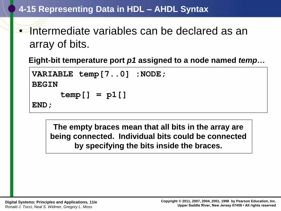
4-15 Representing Data in HDL – AHDL Syntax
VARIABLE temp[7..0] :NODE;
BEGIN
temp[] = p1[]
END;
Eight-bit temperature port p1 assigned to a node named temp…
• Intermediate variables can be declared as an
array of bits.
The empty braces mean that all bits in the array are
being connected. Individual bits could be connected
by specifying the bits inside the braces.
Copyright © 2011, 2007, 2004, 2001, 1998 by Pearson Education, Inc.
Upper Saddle River, New Jersey 07458 • All rights reserved Digital Systems: Principles and Applications, 11/e
Ronald J. Tocci, Neal S. Widmer, Gregory L. Moss
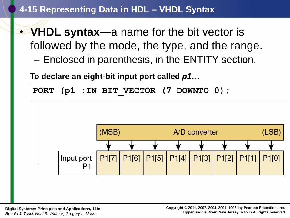
4-15 Representing Data in HDL – VHDL Syntax
• VHDL syntax—a name for the bit vector is
followed by the mode, the type, and the range.
– Enclosed in parenthesis, in the ENTITY section.
PORT (p1 :IN BIT_VECTOR (7 DOWNTO 0);
To declare an eight-bit input port called p1…
Copyright © 2011, 2007, 2004, 2001, 1998 by Pearson Education, Inc.
Upper Saddle River, New Jersey 07458 • All rights reserved Digital Systems: Principles and Applications, 11/e
Ronald J. Tocci, Neal S. Widmer, Gregory L. Moss
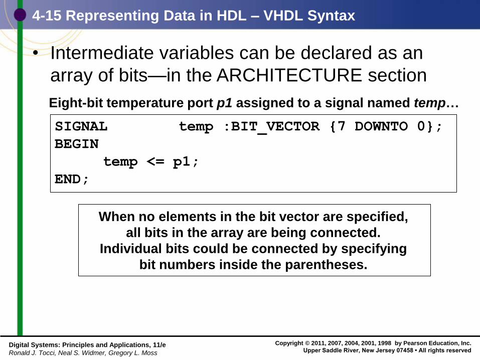
4-15 Representing Data in HDL – VHDL Syntax
SIGNAL temp :BIT_VECTOR {7 DOWNTO 0};
BEGIN
temp <= p1;
END;
Eight-bit temperature port p1 assigned to a signal named temp…
• Intermediate variables can be declared as an
array of bits—in the ARCHITECTURE section
When no elements in the bit vector are specified,
all bits in the array are being connected.
Individual bits could be connected by specifying
bit numbers inside the parentheses.
Copyright © 2011, 2007, 2004, 2001, 1998 by Pearson Education, Inc.
Upper Saddle River, New Jersey 07458 • All rights reserved Digital Systems: Principles and Applications, 11/e
Ronald J. Tocci, Neal S. Widmer, Gregory L. Moss
4-15 Representing Data in HDL
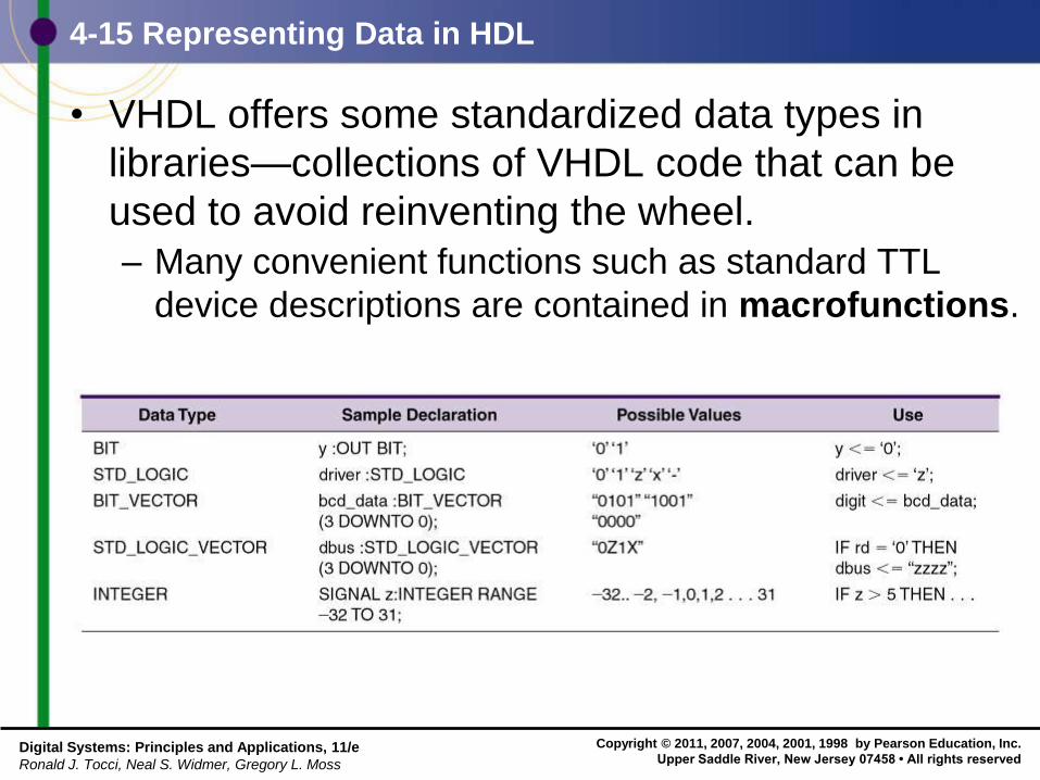
• VHDL offers some standardized data types in
libraries—collections of VHDL code that can be
used to avoid reinventing the wheel.
– Many convenient functions such as standard TTL
device descriptions are contained in macrofunctions.
Copyright © 2011, 2007, 2004, 2001, 1998 by Pearson Education, Inc.
Upper Saddle River, New Jersey 07458 • All rights reserved Digital Systems: Principles and Applications, 11/e
Ronald J. Tocci, Neal S. Widmer, Gregory L. Moss
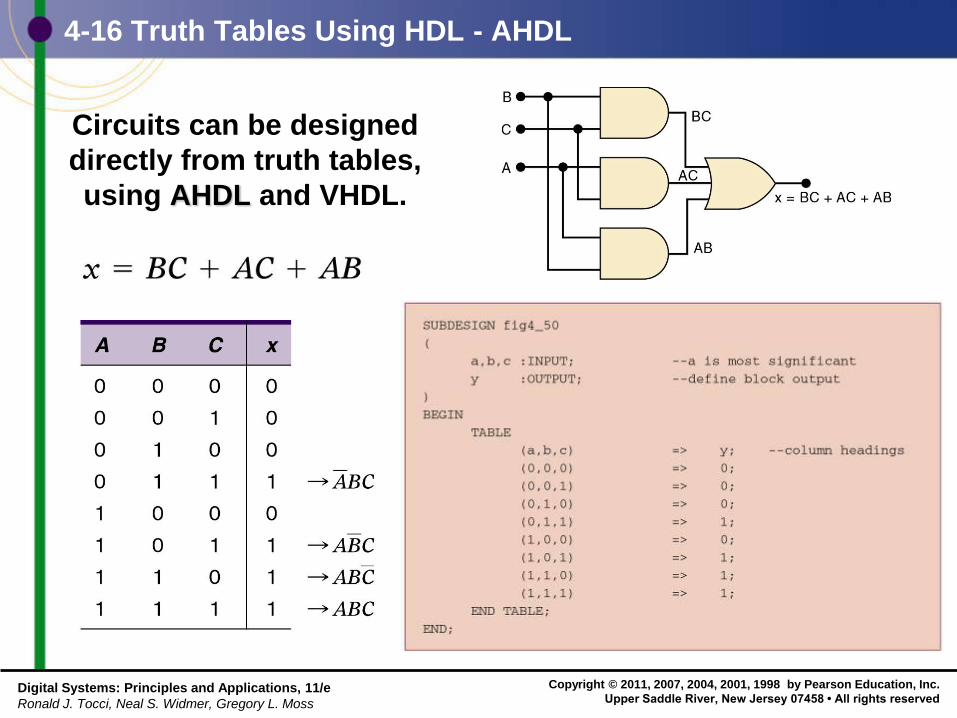
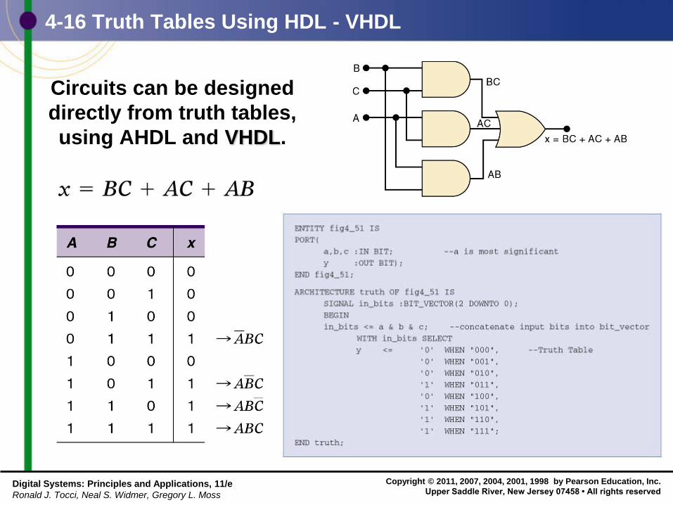
4-16 Truth Tables Using HDL - AHDL
Circuits can be designed
directly from truth tables,
using AHDL and VHDL.
Copyright © 2011, 2007, 2004, 2001, 1998 by Pearson Education, Inc.
Upper Saddle River, New Jersey 07458 • All rights reserved Digital Systems: Principles and Applications, 11/e
Ronald J. Tocci, Neal S. Widmer, Gregory L. Moss
4-16 Truth Tables Using HDL - VHDL
Circuits can be designed
directly from truth tables,
using AHDL and VHDL.
Copyright © 2011, 2007, 2004, 2001, 1998 by Pearson Education, Inc.
Upper Saddle River, New Jersey 07458 • All rights reserved Digital Systems: Principles and Applications, 11/e
Ronald J. Tocci, Neal S. Widmer, Gregory L. Moss
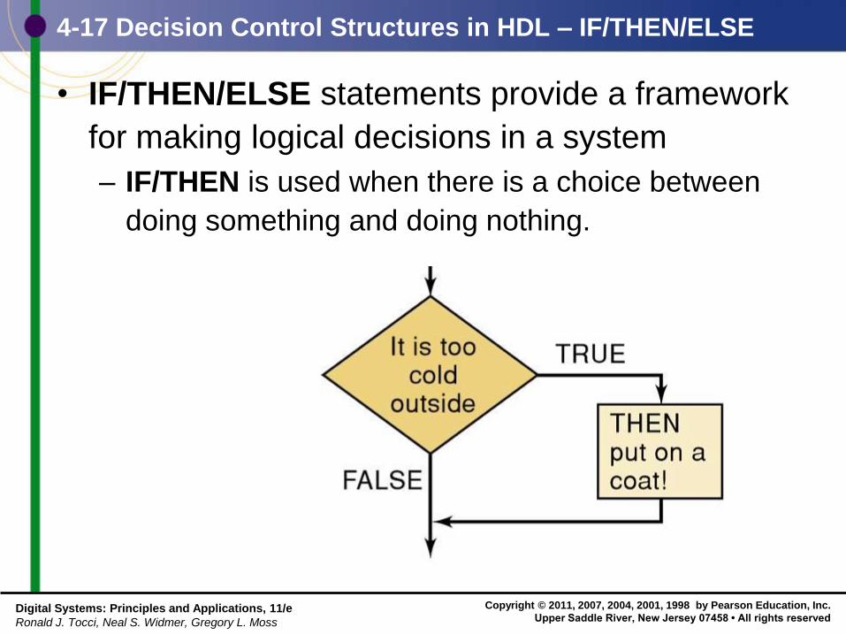
4-17 Decision Control Structures in HDL – IF/THEN/ELSE
• IF/THEN/ELSE statements provide a framework
for making logical decisions in a system
– IF/THEN is used when there is a choice between
doing something and doing nothing.
Copyright © 2011, 2007, 2004, 2001, 1998 by Pearson Education, Inc.
Upper Saddle River, New Jersey 07458 • All rights reserved Digital Systems: Principles and Applications, 11/e
Ronald J. Tocci, Neal S. Widmer, Gregory L. Moss
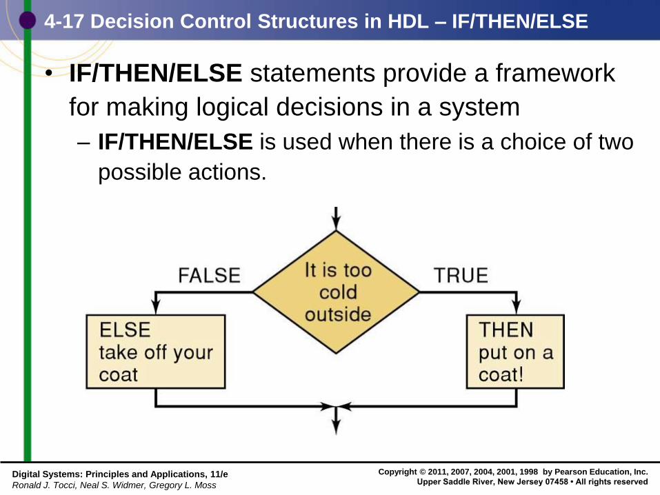
4-17 Decision Control Structures in HDL – IF/THEN/ELSE
• IF/THEN/ELSE statements provide a framework
for making logical decisions in a system
– IF/THEN/ELSE is used when there is a choice of two
possible actions.
Copyright © 2011, 2007, 2004, 2001, 1998 by Pearson Education, Inc.
Upper Saddle River, New Jersey 07458 • All rights reserved Digital Systems: Principles and Applications, 11/e
Ronald J. Tocci, Neal S. Widmer, Gregory L. Moss
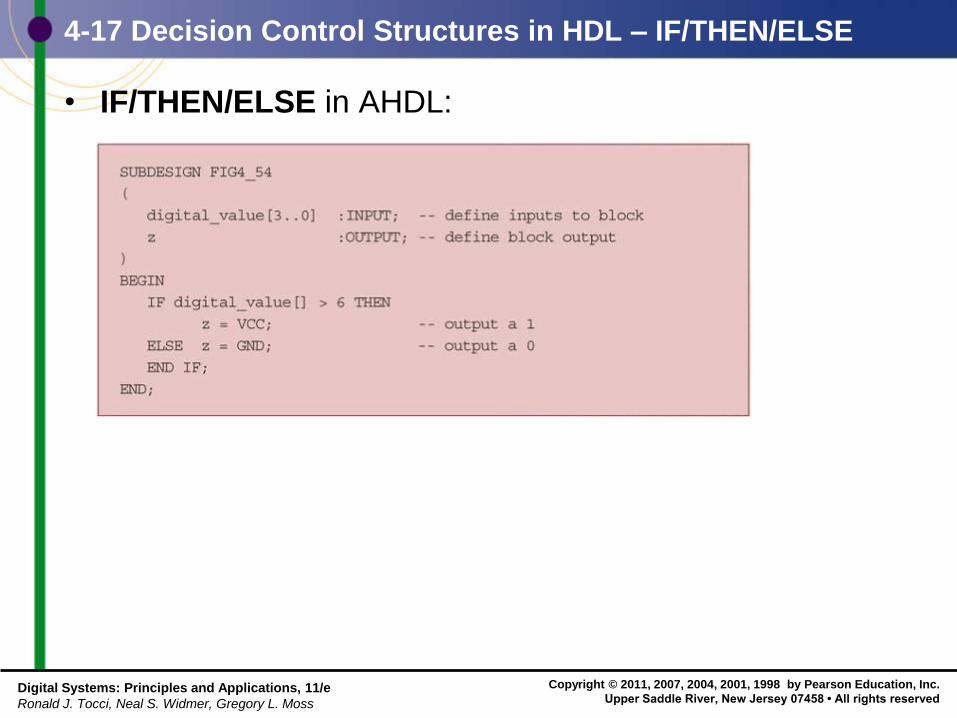
4-17 Decision Control Structures in HDL – IF/THEN/ELSE
• IF/THEN/ELSE in AHDL:
Copyright © 2011, 2007, 2004, 2001, 1998 by Pearson Education, Inc.
Upper Saddle River, New Jersey 07458 • All rights reserved Digital Systems: Principles and Applications, 11/e
Ronald J. Tocci, Neal S. Widmer, Gregory L. Moss
4-17 Decision Control Structures in HDL – IF/THEN/ELSE
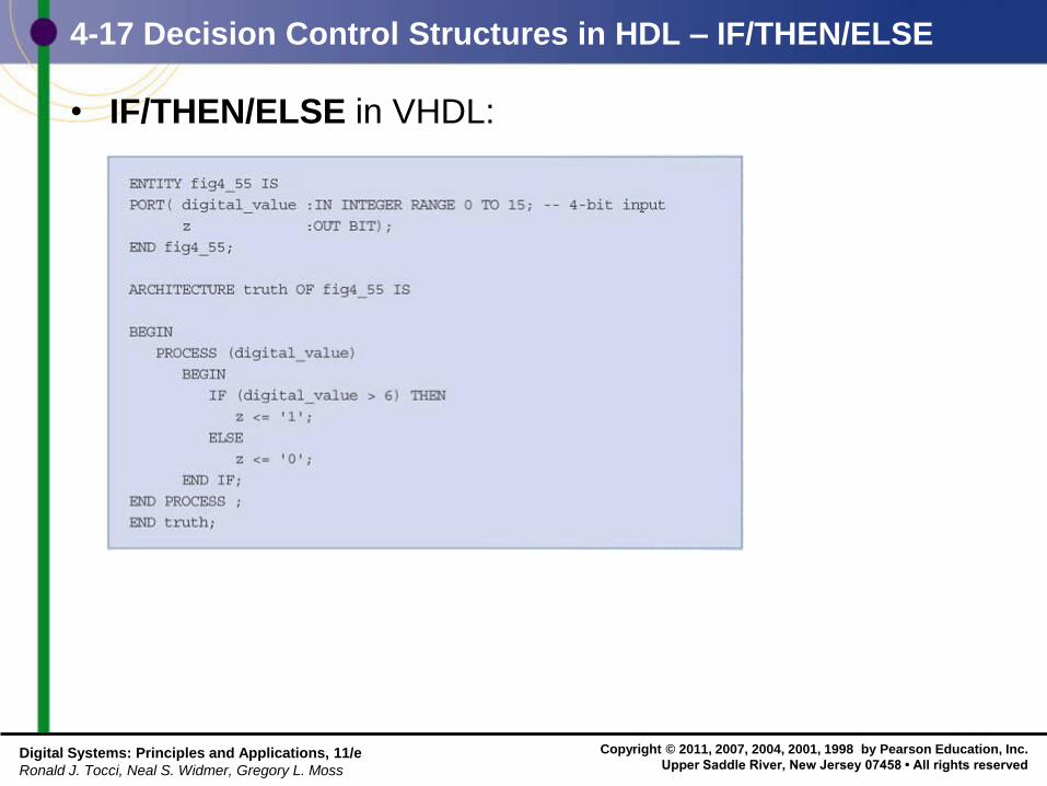
• IF/THEN/ELSE in VHDL:
Copyright © 2011, 2007, 2004, 2001, 1998 by Pearson Education, Inc.
Upper Saddle River, New Jersey 07458 • All rights reserved Digital Systems: Principles and Applications, 11/e
Ronald J. Tocci, Neal S. Widmer, Gregory L. Moss
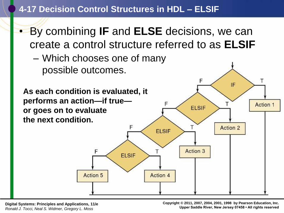
As each condition is evaluated, it
performs an action—if true—
or goes on to evaluate
the next condition.
4-17 Decision Control Structures in HDL – ELSIF
• By combining IF and ELSE decisions, we can
create a control structure referred to as ELSIF
– Which chooses one of many
possible outcomes.
Copyright © 2011, 2007, 2004, 2001, 1998 by Pearson Education, Inc.
Upper Saddle River, New Jersey 07458 • All rights reserved Digital Systems: Principles and Applications, 11/e
Ronald J. Tocci, Neal S. Widmer, Gregory L. Moss
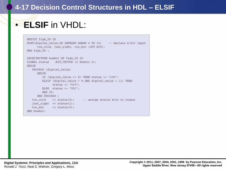
4-17 Decision Control Structures in HDL – ELSIF
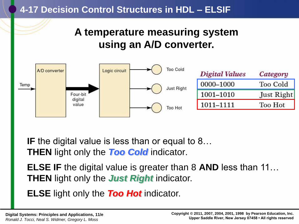
A temperature measuring system
using an A/D converter.
IF the digital value is less than or equal to 8…
THEN light only the Too Cold indicator.
ELSE IF the digital value is greater than 8 AND less than 11…
THEN light only the Just Right indicator.
ELSE light only the Too Hot indicator.
Copyright © 2011, 2007, 2004, 2001, 1998 by Pearson Education, Inc.
Upper Saddle River, New Jersey 07458 • All rights reserved Digital Systems: Principles and Applications, 11/e
Ronald J. Tocci, Neal S. Widmer, Gregory L. Moss
4-17 Decision Control Structures in HDL – ELSIF
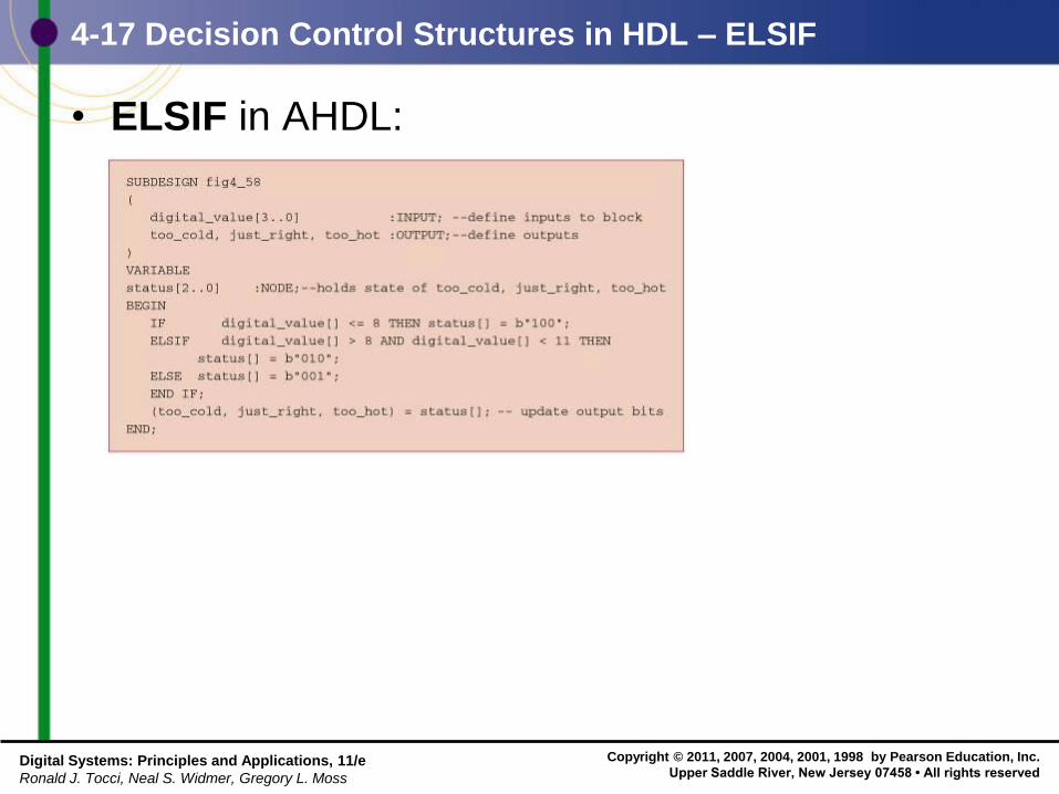
• ELSIF in AHDL:
Copyright © 2011, 2007, 2004, 2001, 1998 by Pearson Education, Inc.
Upper Saddle River, New Jersey 07458 • All rights reserved Digital Systems: Principles and Applications, 11/e
Ronald J. Tocci, Neal S. Widmer, Gregory L. Moss
4-17 Decision Control Structures in HDL – ELSIF
• ELSIF in VHDL:
Copyright © 2011, 2007, 2004, 2001, 1998 by Pearson Education, Inc.
Upper Saddle River, New Jersey 07458 • All rights reserved Digital Systems: Principles and Applications, 11/e
Ronald J. Tocci, Neal S. Widmer, Gregory L. Moss
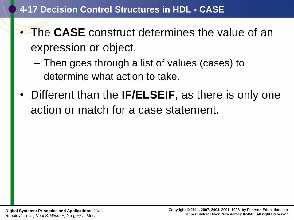
4-17 Decision Control Structures in HDL - CASE
• The CASE construct determines the value of an
expression or object.
– Then goes through a list of values (cases) to
determine what action to take.
• Different than the IF/ELSEIF, as there is only one
action or match for a case statement.
Copyright © 2011, 2007, 2004, 2001, 1998 by Pearson Education, Inc.
Upper Saddle River, New Jersey 07458 • All rights reserved Digital Systems: Principles and Applications, 11/e
Ronald J. Tocci, Neal S. Widmer, Gregory L. Moss
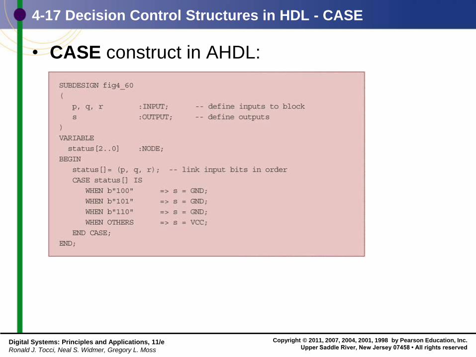
4-17 Decision Control Structures in HDL - CASE
• CASE construct in AHDL:
Copyright © 2011, 2007, 2004, 2001, 1998 by Pearson Education, Inc.
Upper Saddle River, New Jersey 07458 • All rights reserved Digital Systems: Principles and Applications, 11/e
Ronald J. Tocci, Neal S. Widmer, Gregory L. Moss
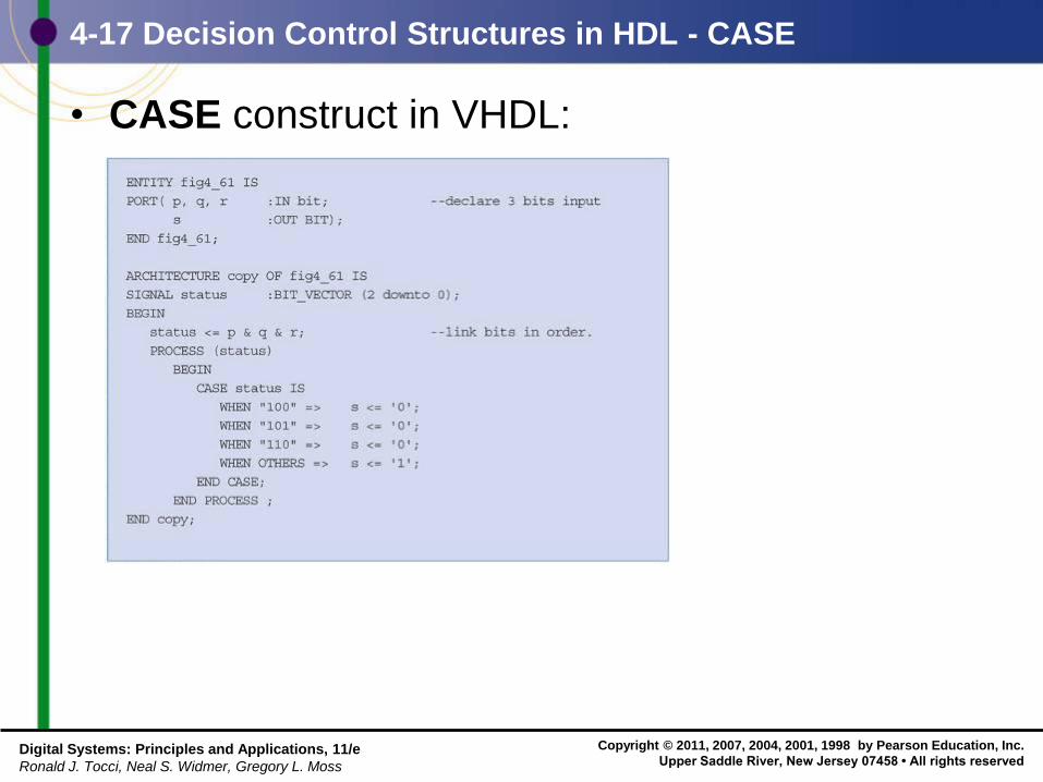
4-17 Decision Control Structures in HDL - CASE
• CASE construct in VHDL:
Copyright © 2011, 2007, 2004, 2001, 1998 by Pearson Education, Inc.
Upper Saddle River, New Jersey 07458 • All rights reserved Digital Systems: Principles and Applications, 11/e
Ronald J. Tocci, Neal S. Widmer, Gregory L. Moss
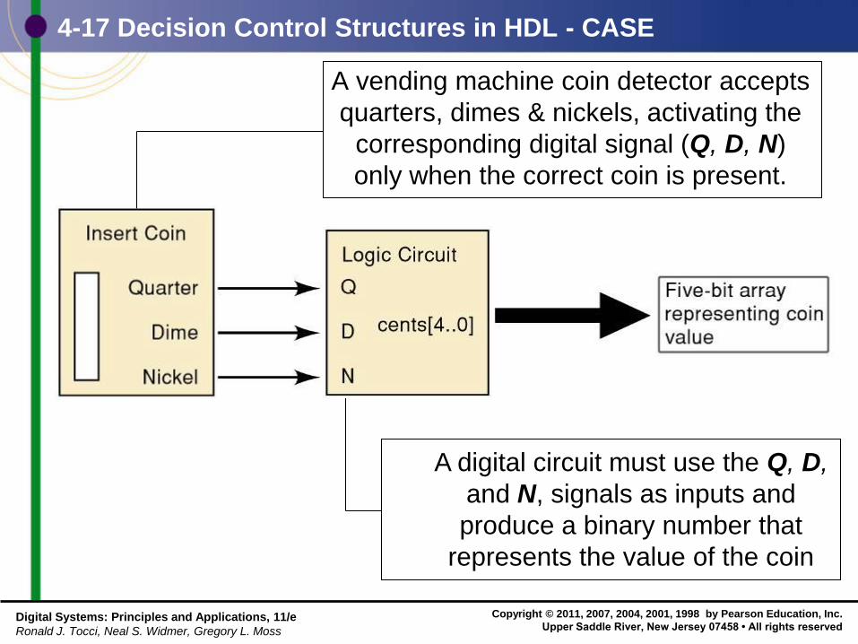
4-17 Decision Control Structures in HDL - CASE
A vending machine coin detector accepts
quarters, dimes & nickels, activating the
corresponding digital signal (Q, D, N)
only when the correct coin is present.
A digital circuit must use the Q, D,
and N, signals as inputs and
produce a binary number that
represents the value of the coin
Copyright © 2011, 2007, 2004, 2001, 1998 by Pearson Education, Inc.
Upper Saddle River, New Jersey 07458 • All rights reserved Digital Systems: Principles and Applications, 11/e
Ronald J. Tocci, Neal S. Widmer, Gregory L. Moss
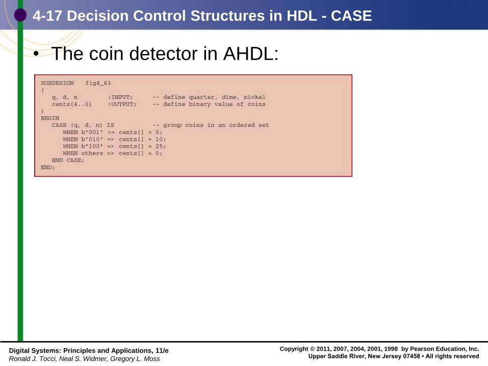
4-17 Decision Control Structures in HDL - CASE
• The coin detector in AHDL:
Copyright © 2011, 2007, 2004, 2001, 1998 by Pearson Education, Inc.
Upper Saddle River, New Jersey 07458 • All rights reserved Digital Systems: Principles and Applications, 11/e
Ronald J. Tocci, Neal S. Widmer, Gregory L. Moss
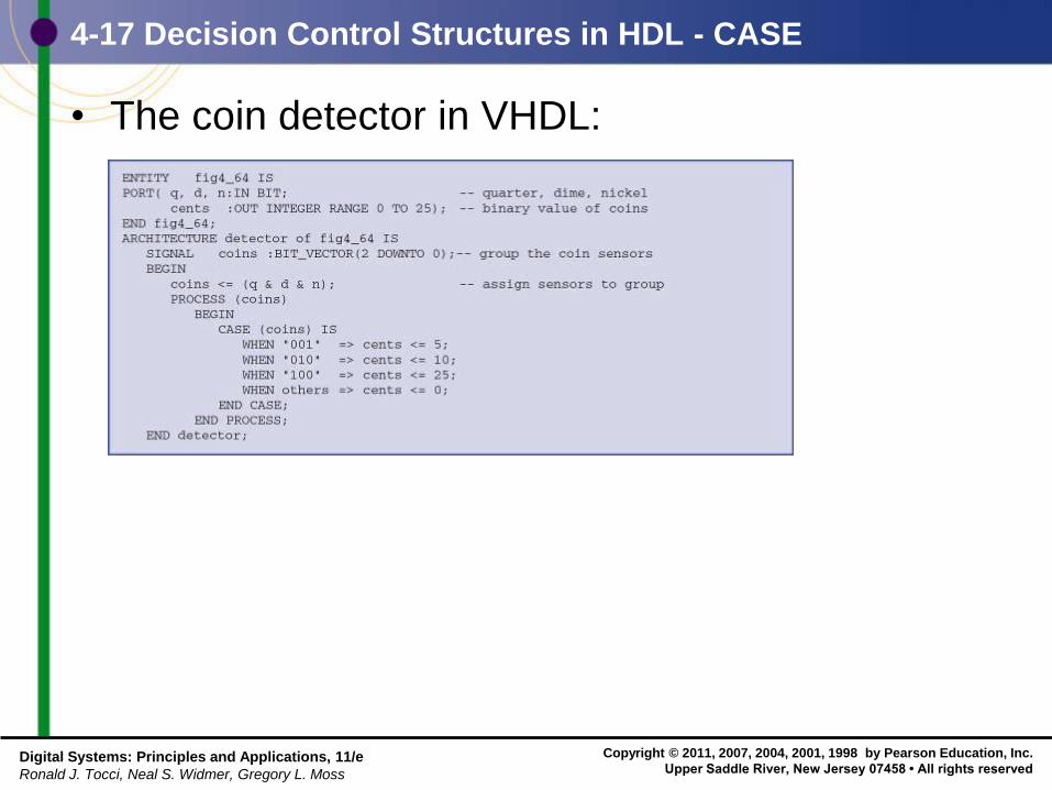
4-17 Decision Control Structures in HDL - CASE
• The coin detector in VHDL:
END
Recommended