8-bit Flash Microcontroller
AT89C51RE2
Features• 80C52 Compatible
– 8051 Instruction Compatible– Four 8-bit I/O Ports (44 Pins Version)– Three 16-bit Timer/Counters– 256 bytes Scratch Pad RAM– 11 Interrupt Sources With 4 Priority Levels
• ISP (In-System Programming) Using Standard VCC Power Supply• Integrated Power Monitor (POR/PFD) to Supervise Internal Power Supply• Boot ROM Contains Serial Loader for In-System Programming• High-speed Architecture
– In Standard Mode: 40 MHz (Vcc 2.7V to 5.5V, Both Internal and External Code Execution)60 MHz (Vcc 4.5V to 5.5V and Internal Code Execution Only)
– In X2 Mode (6 Clocks/Machine Cycle) 20 MHz (Vcc 2.7V to 5.5V, Both Internal and External Code Execution)30 MHz (Vcc 4.5V to 5.5V and Internal Code Execution Only)
• 128K bytes On-chip Flash Program/Data Memory– 128 bytes Page Write with auto-erase– 100k Write Cycles
• On-chip 8192 bytes Expanded RAM (XRAM)– Software Selectable Size (0, 256, 512, 768, 1024, 1792, 2048, 4096, 8192 bytes)
• Dual Data Pointer• Extended stack pointer to 512 bytes• Variable Length MOVX for Slow RAM/Peripherals• Improved X2 Mode with Independant Selection for CPU and Each Peripheral• Keyboard Interrupt Interface on Port 1• SPI Interface (Master/Slave Mode)• 8-bit Clock Prescaler• Programmable Counter Array with:
– High Speed Output– Compare/Capture– Pulse Width Modulator– Watchdog Timer Capabilities
• Asynchronous Port Reset • Two Full Duplex Enhanced UART with Dedicated Internal Baud Rate Generator• Low EMI (inhibit ALE)• Hardware Watchdog Timer (One-time Enabled with Reset-Out), Power-Off Flag• Power Control Modes: Idle Mode, Power-down Mode• Power Supply: 2.7V to 5.5V• Temperature Ranges: Industrial (-40 to +85°C)• Packages: PLCC44, VQFP44
DescriptionAT89C51RE2 is a high performance CMOS Flash version of the 80C51 CMOS single chip 8-bitmicrocontroller. It contains a 128 Kbytes Flash memory block for program.
The 128 Kbytes Flash memory can be programmed either in parallel mode or in serial mode withthe ISP capability or with software. The programming voltage is internally generated from thestandard VCC pin.
The AT89C51RE2 retains all features of the Atmel 80C52 with 256 bytes of internal RAM, a 10-source 4-level interrupt controller and three timer/counters.
In addition, the AT89C51RE2 has a Programmable Counter Array, an XRAM of 8192 bytes, aHardware Watchdog Timer, SPI and Keyboard, two serial channels that facilitates multiproces-sor communication (EUART), a speed improvement mechanism (X2 mode) and an extendedstack mode that allows the stack to be extended in the lower 256 bytes of XRAM.
The fully static design of the AT89C51RE2 allows to reduce system power consumption bybringing the clock frequency down to any value, even DC, without loss of data.
The AT89C51RE2 has 2 software-selectable modes of reduced activity and 8-bit clock prescalerfor further reduction in power consumption. In the Idle mode the CPU is frozen while the periph-erals and the interrupt system are still operating. In the power-down mode the RAM is saved andall other functions are inoperative.
The added features of the AT89C51RE2 make it more powerful for applications that need pulsewidth modulation, high speed I/O and counting capabilities such as alarms, motor control,corded phones, smart card readers.
Table 1. Memory Size and I/O pins
AT89C51RE2 Flash (bytes) XRAM (bytes) TOTAL RAM (bytes) I/O
PLCC44
VQFP44128K 8192 8192 + 256 34
27663E–8051–10/08
AT89C51RE2
AT89C51RE2
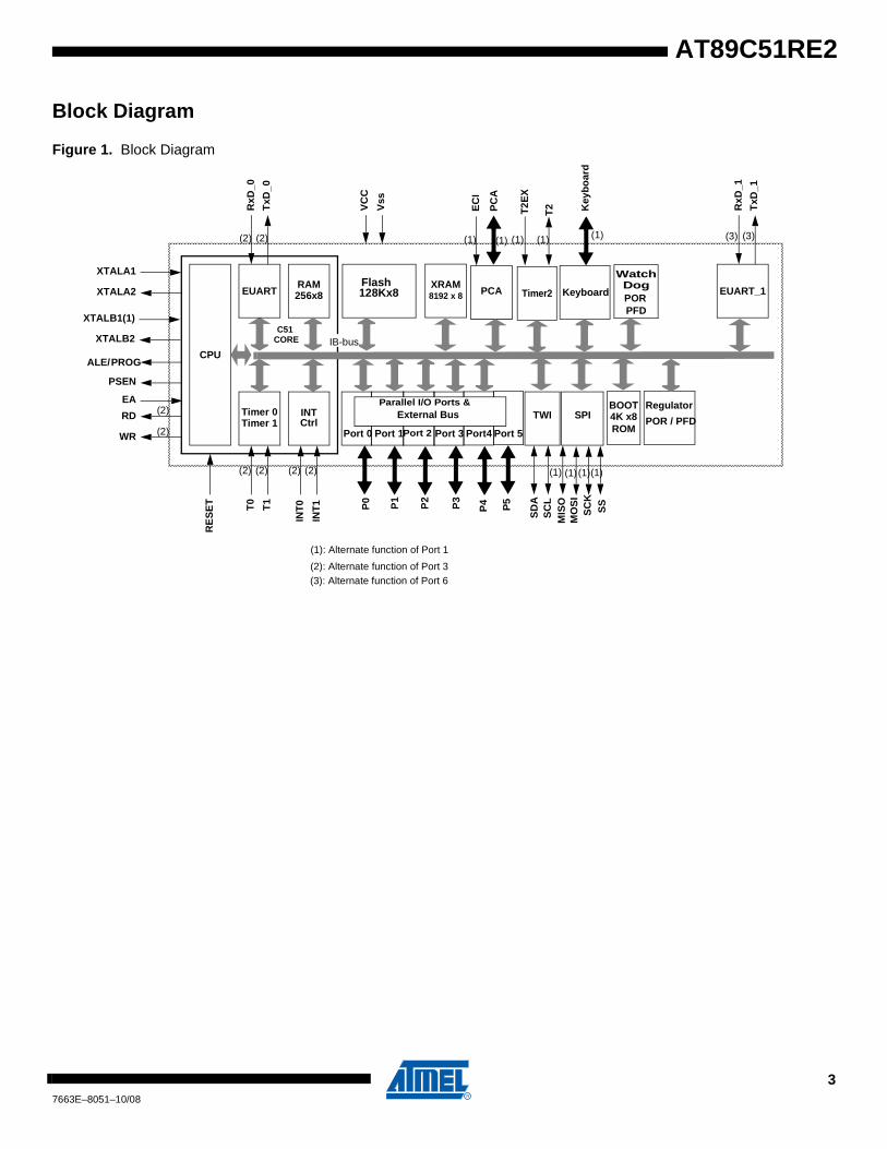
Block Diagram
Figure 1. Block Diagram
Timer 0 INT
RAM256x8
T0
T1
RxD
_0
TxD
_0
WR
RD
EA
PSEN
ALE/
XTALA2
XTALA1
EUART
CPU
Timer 1
INT
1
Ctrl
INT
0
(2)
(2)
C51 CORE
(2) (2) (2) (2)
Port 0
P0
Port 1Port 2 Port 3
P1
P2
P3
XRAM8192 x 8
IB-bus
PCA
RE
SE
T
PROG
WatchDog
PC
A
EC
I
Vss
VC
C
(2)(2) (1)
(1): Alternate function of Port 1
(2): Alternate function of Port 3
(1)
Timer2
T2E
X
T2
(1) (1)
Flash128Kx8 Keyboard
(1)
Key
bo
ard
MIS
OM
OS
IS
CK
SS
(3): Alternate function of Port 6
(3) (3)
Port4
P4
(1) (1) (1)(1)
BOOT4K x8ROM
Regulator
POR / PFDPort 5
P5
Parallel I/O Ports &External Bus SPI
PORPFD
XTALB2
XTALB1(1)
EUART_1
RxD
_1
TxD
_1
TWI
SD
AS
CL
37663E–8051–10/08
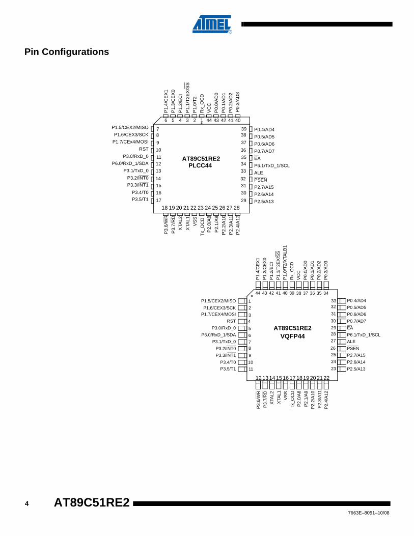
Pin Configurations
43 42 41 40 3944 38 37 36 35 34
P1.
4/C
EX
1
P1.
0/T
2/X
TALB
1
P1.
1/T
2EX
/SS
P1.
3/C
EX
0
P1.
2/E
CI
Rx_
OC
D
VC
C
P0.
0/A
D0
P0.
2/A
D2
P0.
3/A
D3
P0.
1/A
D1
P0.4/AD4
P0.6/AD6
P0.5/AD5
P0.7/AD7
ALE
PSEN
EA
P6.1/TxD_1/SCL
P2.7/A15
P2.5/A13
P2.6/A14
P1.5/CEX2/MISO
P1.6/CEX3/SCKP1.7/CEX4/MOSI
RST
P3.0/RxD_0
P6.0/RxD_1/SDA
P3.1/TxD_0
P3.2/INT0
P3.3/INT1
P3.4/T0
P3.5/T1
P3.
6/W
R
P3.
7/R
D
XTA
L2
XTA
L1
VS
S
P2.
0/A
8
P2.
1/A
9
P2.
2/A
10
P2.
3/A
11
P2.
4/A
12
Tx_
OC
D
12 13 17161514 201918 21 22
3332
31
30
2928
27
26
25
24
23
1
2
3 4
5
6
78
9
10
11
VQFP44
PLCC44
AT89C51RE2
AT89C51RE2
18 19 23222120 262524 27 28
5 4 3 2 1 6 44 43 42 41 40
P1.
4/C
EX
1
P1.
0/T
2
P1.
1/T
2EX
/SS
P1.
3/C
EX
0
P1.
2/E
CI
Rx_
OC
D
VC
C
P0.
0/A
D0
P0.
2/A
D2
P0.
1/A
D1
P0.4/AD4
P0.6/AD6
P0.5/AD5
P0.7/AD7
ALE
PSEN
EA
P6.1/TxD_1/SCL
P2.7/A15
P2.5/A13
P2.6/A14
P3.
6/W
R
P3.
7/R
D
XTA
L2
XTA
L1
VS
S
P2.
0/A
8
P2.
1/A
9
P2.
2/A
10
P2.
3/A
11
P2.
4/A
12
P1.5/CEX2/MISO
P1.6/CEX3/SCK
P1.7/CEx4/MOSI
RST
P3.0/RxD_0
P6.0/RxD_1/SDA
P3.1/TxD_0
P3.2/INT0
P3.3/INT1
P3.4/T0
P3.5/T1
P0.
3/A
D3
Tx_
OC
D
78
9
10
1112
13
14
15
16
17
3938
37
36
3534
33
32
31
30
29
47663E–8051–10/08
AT89C51RE2

AT89C51RE2
Table 2. Pin Description
Mnemonic
Pin Number
Type Name and FunctionLCC VQFP 1.4
VSS 22 16 I Ground: 0V reference
Vss1 39 I Optional Ground: Contact the Sales Office for ground connection.
VCC 44 38 I Power Supply: This is the power supply voltage for normal, idle and power-down operation
P0.0-P0.7 43-36 37-30 I/O Port 0: Port 0 is an open-drain, bidirectional I/O port. Port 0 pins that have 1s written to them float and can be used as high impedance inputs. Port 0 must be polarized to VCC or VSS in order to prevent any parasitic current consumption. Port 0 is also the multiplexed low-order address and data bus during access to external program and data memory. In this application, it uses strong internal pull-up when emitting 1s. Port 0 also inputs the code bytes during EPROM programming. External pull-ups are required during program verification during which P0 outputs the code bytes.
P1.0-P1.7 2-9 40-441-3
I/O Port 1: Port 1 is an 8-bit bidirectional I/O port with internal pull-ups. Port 1 pins that have 1s written to them are pulled high by the internal pull-ups and can be used as inputs. As inputs, Port 1 pins that are externally pulled low will source current because of the internal pull-ups. Port 1 also receives the low-order address byte during memory programming and verification.
Alternate functions for TSC8x54/58 Port 1 include:
2 40 I/O T2 (P1.0): Timer/Counter 2 external count input/Clockout
3 41 I T2EX (P1.1): Timer/Counter 2 Reload/Capture/Direction Control
4 42 I ECI (P1.2): External Clock for the PCA
5 43 I/O CEX0 (P1.3): Capture/Compare External I/O for PCA module 0
6 44 I/O CEX1 (P1.4): Capture/Compare External I/O for PCA module 1
7 1 I/O CEX2 (P1.5): Capture/Compare External I/O for PCA module 2
8 2 I/O CEX3 (P1.6): Capture/Compare External I/O for PCA module 3
9 3 I/O CEX4 (P1.7): Capture/Compare External I/O for PCA module 4
P2.0-P2.7 24-31 18-25 I/O Port 2: Port 2 is an 8-bit bidirectional I/O port with internal pull-ups. Port 2 pins that have 1s written to them are pulled high by the internal pull-ups and can be used as inputs. As inputs, Port 2 pins that are externally pulled low will source current because of the internal pull-ups. Port 2 emits the high-order address byte during fetches from external program memory and during accesses to external data memory that use 16-bit addresses (MOVX @DPTR).In this application, it uses strong internal pull-ups emitting 1s. During accesses to external data memory that use 8-bit addresses (MOVX @Ri), port 2 emits the contents of the P2 SFR. Some Port 2 pins receive the high order address bits during EPROM programming and verification:
P2.0 to P2.5 for RB devices
P2.0 to P2.6 for RC devices
P2.0 to P2.7 for RD devices.
P3.0-P3.7 11,13-19
5,7-13
I/O Port 3: Port 3 is an 8-bit bidirectional I/O port with internal pull-ups. Port 3 pins that have 1s written to them are pulled high by the internal pull-ups and can be used as inputs. As inputs, Port 3 pins that are externally pulled low will source current because of the internal pull-ups. Port 3 also serves the special features of the 80C51 family, as listed below.
11 5 I RXD_0 (P3.0): Serial input port
13 7 O TXD_0 (P3.1): Serial output port
14 8 I INT0 (P3.2): External interrupt 0
57663E–8051–10/08
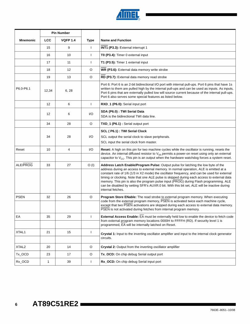
15 9 I INT1 (P3.3): External interrupt 1
16 10 I T0 (P3.4): Timer 0 external input
17 11 I T1 (P3.5): Timer 1 external input
18 12 O WR (P3.6): External data memory write strobe
19 13 O RD (P3.7): External data memory read strobe
P6.0-P6.112,34 6, 28
Port 6: Port 6 is an 2-bit bidirectional I/O port with internal pull-ups. Port 6 pins that have 1s written to them are pulled high by the internal pull-ups and can be used as inputs. As inputs, Port 6 pins that are externally pulled low will source current because of the internal pull-ups. Port 6 also serves some special features as listed below.
12 6 I RXD_1 (P6.0): Serial input port
12 6 I/OSDA (P6.0) : TWI Serial Data
SDA is the bidirectional TWI data line.
34 28 O TXD_1 (P6.1) : Serial output port
34 28 I/O
SCL ( P6.1) : TWI Serial Clock
SCL output the serial clock to slave peripherals.
SCL input the serial clock from master.
Reset 10 4 I/O Reset: A high on this pin for two machine cycles while the oscillator is running, resets the device. An internal diffused resistor to VSS permits a power-on reset using only an external capacitor to VCC. This pin is an output when the hardware watchdog forces a system reset.
ALE/PROG 33 27 O (I) Address Latch Enable/Program Pulse: Output pulse for latching the low byte of the address during an access to external memory. In normal operation, ALE is emitted at a constant rate of 1/6 (1/3 in X2 mode) the oscillator frequency, and can be used for external timing or clocking. Note that one ALE pulse is skipped during each access to external data memory. This pin is also the program pulse input (PROG) during Flash programming. ALE can be disabled by setting SFR’s AUXR.0 bit. With this bit set, ALE will be inactive during internal fetches.
PSEN 32 26 O Program Store ENable: The read strobe to external program memory. When executing code from the external program memory, PSEN is activated twice each machine cycle, except that two PSEN activations are skipped during each access to external data memory. PSEN is not activated during fetches from internal program memory.
EA 35 29 I External Access Enable: EA must be externally held low to enable the device to fetch code from external program memory locations 0000H to FFFFH (RD). If security level 1 is programmed, EA will be internally latched on Reset.
XTAL1 21 15 I Crystal 1: Input to the inverting oscillator amplifier and input to the internal clock generator circuits.
XTAL2 20 14 O Crystal 2: Output from the inverting oscillator amplifier
Tx_OCD 23 17 O Tx_OCD: On chip debug Serial output port
Rx_OCD 1 39 I Rx_OCD: On chip debug Serial input port
Mnemonic
Pin Number
Type Name and FunctionLCC VQFP 1.4
67663E–8051–10/08
AT89C51RE2

AT89C51RE2
SFR Mapping The Special Function Registers (SFRs) of the AT89C51RE2 fall into the following categories:
• C51 core registers: ACC, B, DPH, DPL, PSW, SP
• I/O port registers: P0, P1, P2, P3, P4, P5, P6
• Timer registers: T2CON, T2MOD, TCON, TH0, TH1, TH2, TMOD, TL0, TL1, TL2, RCAP2L, RCAP2H
• Serial I/O port registers: SADDR_0, SADEN_0, SBUF_0, SCON_0, SADDR_1, SADEN_1, SBUF_1, SCON_1,
• PCA (Programmable Counter Array) registers: CCON, CCAPMx, CL, CH, CCAPxH, CCAPxL (x: 0 to 4)
• Power and clock control registers: PCON, CKAL, CKCON0_1
• Hardware Watchdog Timer registers: WDTRST, WDTPRG
• Interrupt system registers: IE0, IPL0, IPH0, IE1, IPL1, IPH1
• Keyboard Interface registers: KBE, KBF, KBLS
• 2-wire Interface registers: SSCON, SSCS, SSDAT, SSADR
• SPI registers: SPCON, SPSTR, SPDAT
• BRG (Baud Rate Generator) registers: BRL_0, BRL_1, BDRCON_0, BDRCON_1
• Memory register: FCON, FSTA
• Clock Prescaler register: CKRL
• Others: AUXR, AUXR1, CKCON0, CKCON1, BMSEL
77663E–8051–10/08
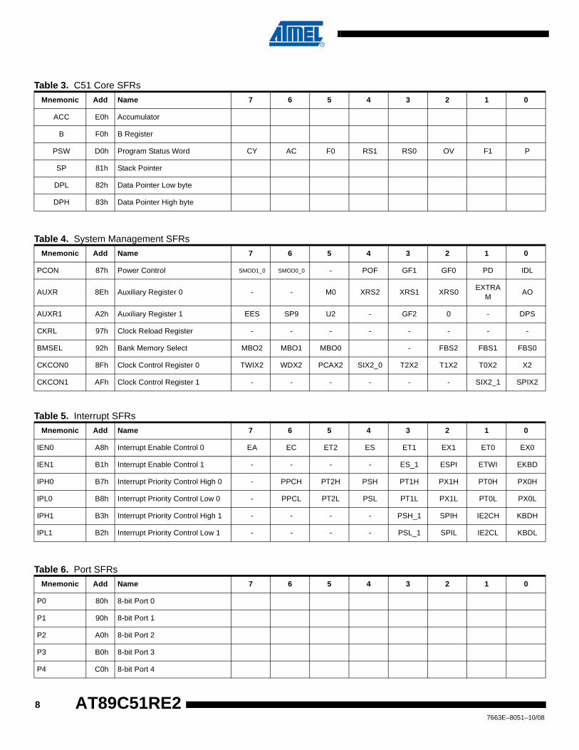
Table 3. C51 Core SFRs
Mnemonic Add Name 7 6 5 4 3 2 1 0
ACC E0h Accumulator
B F0h B Register
PSW D0h Program Status Word CY AC F0 RS1 RS0 OV F1 P
SP 81h Stack Pointer
DPL 82h Data Pointer Low byte
DPH 83h Data Pointer High byte
Table 4. System Management SFRs
Mnemonic Add Name 7 6 5 4 3 2 1 0
PCON 87h Power Control SMOD1_0 SMOD0_0 - POF GF1 GF0 PD IDL
AUXR 8Eh Auxiliary Register 0 - - M0 XRS2 XRS1 XRS0EXTRA
MAO
AUXR1 A2h Auxiliary Register 1 EES SP9 U2 - GF2 0 - DPS
CKRL 97h Clock Reload Register - - - - - - - -
BMSEL 92h Bank Memory Select MBO2 MBO1 MBO0 - FBS2 FBS1 FBS0
CKCON0 8Fh Clock Control Register 0 TWIX2 WDX2 PCAX2 SIX2_0 T2X2 T1X2 T0X2 X2
CKCON1 AFh Clock Control Register 1 - - - - - - SIX2_1 SPIX2
Table 5. Interrupt SFRs
Mnemonic Add Name 7 6 5 4 3 2 1 0
IEN0 A8h Interrupt Enable Control 0 EA EC ET2 ES ET1 EX1 ET0 EX0
IEN1 B1h Interrupt Enable Control 1 - - - - ES_1 ESPI ETWI EKBD
IPH0 B7h Interrupt Priority Control High 0 - PPCH PT2H PSH PT1H PX1H PT0H PX0H
IPL0 B8h Interrupt Priority Control Low 0 - PPCL PT2L PSL PT1L PX1L PT0L PX0L
IPH1 B3h Interrupt Priority Control High 1 - - - - PSH_1 SPIH IE2CH KBDH
IPL1 B2h Interrupt Priority Control Low 1 - - - - PSL_1 SPIL IE2CL KBDL
Table 6. Port SFRs
Mnemonic Add Name 7 6 5 4 3 2 1 0
P0 80h 8-bit Port 0
P1 90h 8-bit Port 1
P2 A0h 8-bit Port 2
P3 B0h 8-bit Port 3
P4 C0h 8-bit Port 4
87663E–8051–10/08
AT89C51RE2
AT89C51RE2
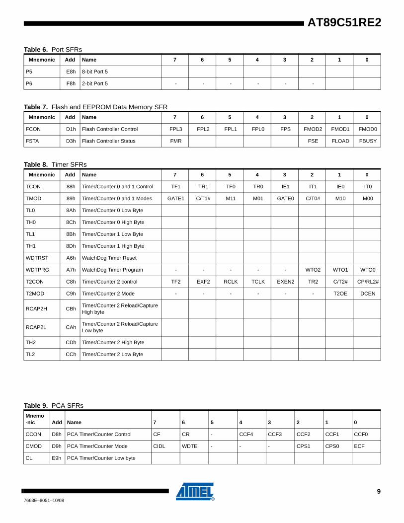
P5 E8h 8-bit Port 5
P6 F8h 2-bit Port 5 - - - - - -
Table 6. Port SFRs
Mnemonic Add Name 7 6 5 4 3 2 1 0
Table 7. Flash and EEPROM Data Memory SFR
Mnemonic Add Name 7 6 5 4 3 2 1 0
FCON D1h Flash Controller Control FPL3 FPL2 FPL1 FPL0 FPS FMOD2 FMOD1 FMOD0
FSTA D3h Flash Controller Status FMR FSE FLOAD FBUSY
Table 8. Timer SFRs
Mnemonic Add Name 7 6 5 4 3 2 1 0
TCON 88h Timer/Counter 0 and 1 Control TF1 TR1 TF0 TR0 IE1 IT1 IE0 IT0
TMOD 89h Timer/Counter 0 and 1 Modes GATE1 C/T1# M11 M01 GATE0 C/T0# M10 M00
TL0 8Ah Timer/Counter 0 Low Byte
TH0 8Ch Timer/Counter 0 High Byte
TL1 8Bh Timer/Counter 1 Low Byte
TH1 8Dh Timer/Counter 1 High Byte
WDTRST A6h WatchDog Timer Reset
WDTPRG A7h WatchDog Timer Program - - - - - WTO2 WTO1 WTO0
T2CON C8h Timer/Counter 2 control TF2 EXF2 RCLK TCLK EXEN2 TR2 C/T2# CP/RL2#
T2MOD C9h Timer/Counter 2 Mode - - - - - - T2OE DCEN
RCAP2H CBhTimer/Counter 2 Reload/Capture High byte
RCAP2L CAhTimer/Counter 2 Reload/Capture Low byte
TH2 CDh Timer/Counter 2 High Byte
TL2 CCh Timer/Counter 2 Low Byte
Table 9. PCA SFRs
Mnemo-nic Add Name 7 6 5 4 3 2 1 0
CCON D8h PCA Timer/Counter Control CF CR - CCF4 CCF3 CCF2 CCF1 CCF0
CMOD D9h PCA Timer/Counter Mode CIDL WDTE - - - CPS1 CPS0 ECF
CL E9h PCA Timer/Counter Low byte
97663E–8051–10/08

CH F9h PCA Timer/Counter High byte
CCAPM0
CCAPM1
CCAPM2
CCAPM3
CCAPM4
DAh
DBh
DCh
DDh
DEh
PCA Timer/Counter Mode 0
PCA Timer/Counter Mode 1
PCA Timer/Counter Mode 2
PCA Timer/Counter Mode 3
PCA Timer/Counter Mode 4
-
ECOM0
ECOM1
ECOM2
ECOM3
ECOM4
CAPP0
CAPP1
CAPP2
CAPP3
CAPP4
CAPN0
CAPN1
CAPN2
CAPN3
CAPN4
MAT0
MAT1
MAT2
MAT3
MAT4
TOG0
TOG1
TOG2
TOG3
TOG4
PWM0
PWM1
PWM2
PWM3
PWM4
ECCF0
ECCF1
ECCF2
ECCF3
ECCF4
CCAP0H
CCAP1H
CCAP2H
CCAP3H
CCAP4H
FAh
FBh
FCh
FDh
FEh
PCA Compare Capture Module 0 H
PCA Compare Capture Module 1 H
PCA Compare Capture Module 2 H
PCA Compare Capture Module 3 H
PCA Compare Capture Module 4 H
CCAP0H7
CCAP1H7
CCAP2H7
CCAP3H7
CCAP4H7
CCAP0H6
CCAP1H6
CCAP2H6
CCAP3H6
CCAP4H6
CCAP0H5
CCAP1H5
CCAP2H5
CCAP3H5
CCAP4H5
CCAP0H4
CCAP1H4
CCAP2H4
CCAP3H4
CCAP4H4
CCAP0H3
CCAP1H3
CCAP2H3
CCAP3H3
CCAP4H3
CCAP0H2
CCAP1H2
CCAP2H2
CCAP3H2
CCAP4H2
CCAP0H1
CCAP1H1
CCAP2H1
CCAP3H1
CCAP4H1
CCAP0H0
CCAP1H0
CCAP2H0
CCAP3H0
CCAP4H0
CCAP0L
CCAP1L
CCAP2L
CCAP3L
CCAP4L
EAh
EBh
ECh
EDh
EEh
PCA Compare Capture Module 0 L
PCA Compare Capture Module 1 L
PCA Compare Capture Module 2 L
PCA Compare Capture Module 3 L
PCA Compare Capture Module 4 L
CCAP0L7
CCAP1L7
CCAP2L7
CCAP3L7
CCAP4L7
CCAP0L6
CCAP1L6
CCAP2L6
CCAP3L6
CCAP4L6
CCAP0L5
CCAP1L5
CCAP2L5
CCAP3L5
CCAP4L5
CCAP0L4
CCAP1L4
CCAP2L4
CCAP3L4
CCAP4L4
CCAP0L3
CCAP1L3
CCAP2L3
CCAP3L3
CCAP4L3
CCAP0L2
CCAP1L2
CCAP2L2
CCAP3L2
CCAP4L2
CCAP0L1
CCAP1L1
CCAP2L1
CCAP3L1
CCAP4L1
CCAP0L0
CCAP1L0
CCAP2L0
CCAP3L0
CCAP4L0
Table 10. Serial I/O Port SFRs
Mnemonic Add Name 7 6 5 4 3 2 1 0
SCON_0 98h Serial Control 0 FE/SM0_0 SM1_0 SM2_0 REN_0 TB8_0 RB8_0 TI_0 RI_0
SBUF_0 99h Serial Data Buffer 0
SADEN_0 B9h Slave Address Mask 0
SADDR_0 A9h Slave Address 0
BDRCON_0 9Bh Baud Rate Control 0 BRR_0 TBCK_0 RBCK_0 SPD_0 SRC_0
BRL_0 9Ah Baud Rate Reload 0
SCON_1 C0h Serial Control 1 FE_1/SM0_1 SM1_1 SM2_1 REN_1 TB8_1 RB8_1 TI_1 RI_1
SBUF_1 C1h Serial Data Buffer 1
SADEN_1 BAh Slave Address Mask 1
SADDR_1 AAh Slave Address 1
BDRCON_1 BCh Baud Rate Control 1 SMOD1_1 SMOD0_1 BRR_1 TBCK_1 RBCK_1 SPD_1 SRC_1
BRL_1 BBh Baud Rate Reload 1
Table 9. PCA SFRs (Continued)
Mnemo-nic Add Name 7 6 5 4 3 2 1 0
107663E–8051–10/08
AT89C51RE2
AT89C51RE2
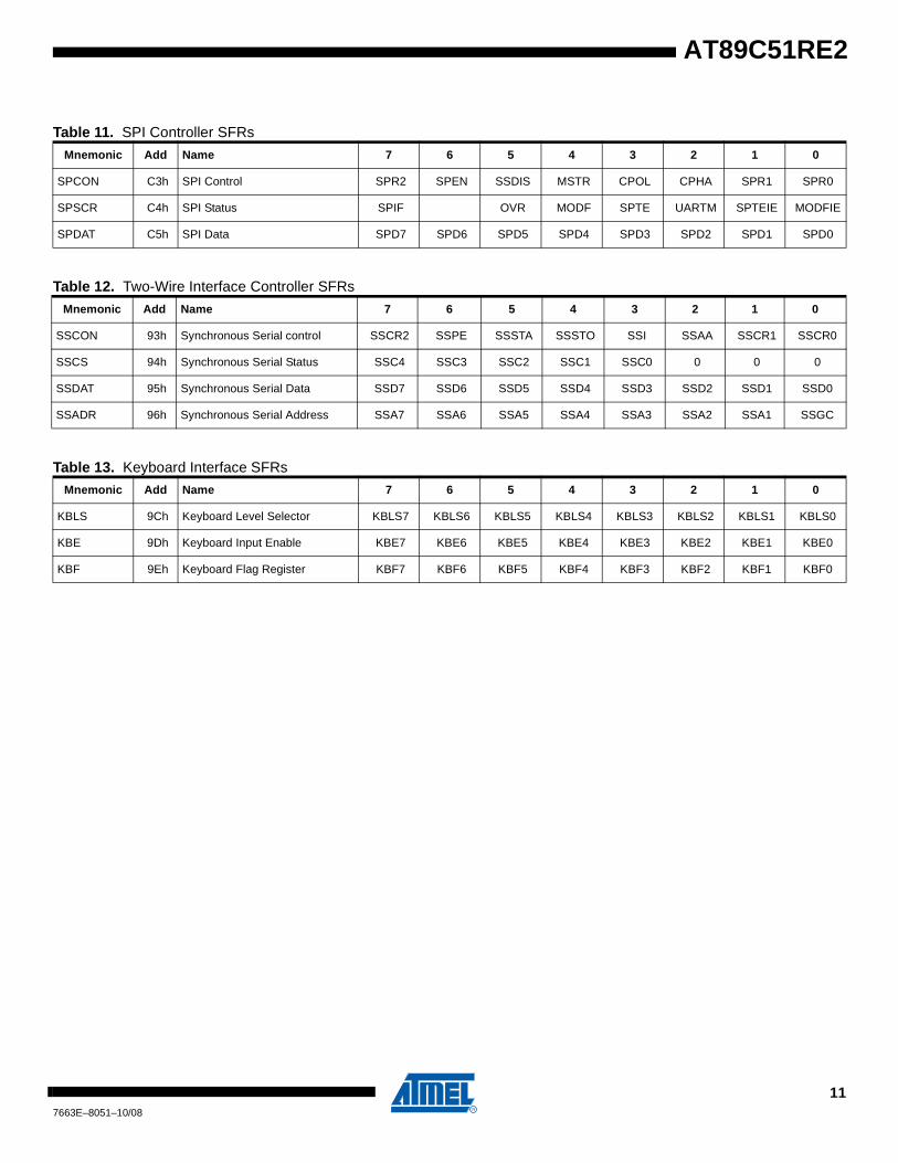
Table 11. SPI Controller SFRs
Mnemonic Add Name 7 6 5 4 3 2 1 0
SPCON C3h SPI Control SPR2 SPEN SSDIS MSTR CPOL CPHA SPR1 SPR0
SPSCR C4h SPI Status SPIF OVR MODF SPTE UARTM SPTEIE MODFIE
SPDAT C5h SPI Data SPD7 SPD6 SPD5 SPD4 SPD3 SPD2 SPD1 SPD0
Table 12. Two-Wire Interface Controller SFRs
Mnemonic Add Name 7 6 5 4 3 2 1 0
SSCON 93h Synchronous Serial control SSCR2 SSPE SSSTA SSSTO SSI SSAA SSCR1 SSCR0
SSCS 94h Synchronous Serial Status SSC4 SSC3 SSC2 SSC1 SSC0 0 0 0
SSDAT 95h Synchronous Serial Data SSD7 SSD6 SSD5 SSD4 SSD3 SSD2 SSD1 SSD0
SSADR 96h Synchronous Serial Address SSA7 SSA6 SSA5 SSA4 SSA3 SSA2 SSA1 SSGC
Table 13. Keyboard Interface SFRs
Mnemonic Add Name 7 6 5 4 3 2 1 0
KBLS 9Ch Keyboard Level Selector KBLS7 KBLS6 KBLS5 KBLS4 KBLS3 KBLS2 KBLS1 KBLS0
KBE 9Dh Keyboard Input Enable KBE7 KBE6 KBE5 KBE4 KBE3 KBE2 KBE1 KBE0
KBF 9Eh Keyboard Flag Register KBF7 KBF6 KBF5 KBF4 KBF3 KBF2 KBF1 KBF0
117663E–8051–10/08
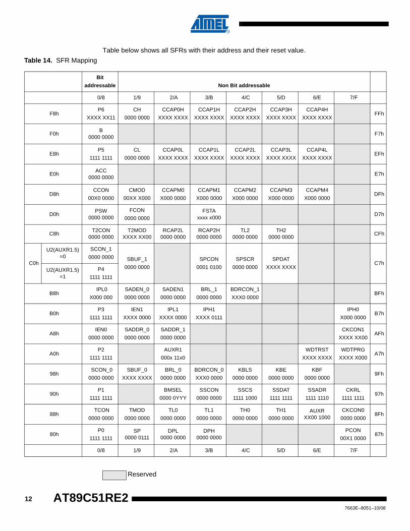
Table below shows all SFRs with their address and their reset value.
Table 14. SFR Mapping
Bit
addressable Non Bit addressable
0/8 1/9 2/A 3/B 4/C 5/D 6/E 7/F
F8hP6
XXXX XX11
CH
0000 0000
CCAP0H
XXXX XXXX
CCAP1H
XXXX XXXX
CCAP2H
XXXX XXXX
CCAP3H
XXXX XXXX
CCAP4H
XXXX XXXXFFh
F0hB
0000 0000F7h
E8hP5
1111 1111
CL
0000 0000
CCAP0L
XXXX XXXX
CCAP1L
XXXX XXXX
CCAP2L
XXXX XXXX
CCAP3L
XXXX XXXX
CCAP4L
XXXX XXXXEFh
E0hACC
0000 0000E7h
D8hCCON
00X0 0000
CMOD
00XX X000
CCAPM0
X000 0000
CCAPM1
X000 0000
CCAPM2
X000 0000
CCAPM3
X000 0000
CCAPM4
X000 0000DFh
D0hPSW
0000 0000FCON
0000 0000FSTA
xxxx x000D7h
C8hT2CON
0000 0000T2MOD
XXXX XX00RCAP2L
0000 0000RCAP2H
0000 0000TL2
0000 0000TH2
0000 0000CFh
C0h
U2(AUXR1.5)=0
SCON_1
0000 0000 SBUF_1
0000 0000
SPCON
0001 0100
SPSCR
0000 0000
SPDAT
XXXX XXXXC7h
U2(AUXR1.5)=1
P4
1111 1111
B8h IPL0
X000 000
SADEN_0
0000 0000
SADEN1
0000 0000
BRL_1
0000 0000
BDRCON_1
XXX0 0000BFh
B0hP3
1111 1111
IEN1
XXXX 0000
IPL1
XXXX 0000
IPH1
XXXX 0111
IPH0
X000 0000B7h
A8hIEN0
0000 0000
SADDR_0
0000 0000
SADDR_1
0000 0000
CKCON1
XXXX XX00AFh
A0hP2
1111 1111
AUXR1
000x 11x0
WDTRST
XXXX XXXX
WDTPRG
XXXX X000A7h
98h SCON_0
0000 0000
SBUF_0
XXXX XXXX
BRL_0
0000 0000
BDRCON_0
XXX0 0000
KBLS
0000 0000
KBE
0000 0000
KBF
0000 00009Fh
90hP1
1111 1111
BMSEL
0000 0YYY
SSCON
0000 0000
SSCS
1111 1000
SSDAT
1111 1111
SSADR
1111 1110
CKRL
1111 111197h
88h TCON
0000 0000
TMOD
0000 0000
TL0
0000 0000
TL1
0000 0000
TH0
0000 0000
TH1
0000 0000AUXR
XX00 1000CKCON0
0000 00008Fh
80hP0
1111 1111SP
0000 0111DPL
0000 0000DPH
0000 0000PCON
00X1 000087h
0/8 1/9 2/A 3/B 4/C 5/D 6/E 7/F
Reserved
127663E–8051–10/08
AT89C51RE2
AT89C51RE2
Enhanced Features
In comparison to the original 80C52, the AT89C51RE2 implements some new features, whichare:
• X2 option
• Dual Data Pointer
• Extended RAM
• Extended stack
• Programmable Counter Array (PCA)
• Hardware Watchdog
• SPI interface
• 4-level interrupt priority system
• power-off flag
• ONCE mode
• ALE disabling
• Enhanced features on the UART and the timer 2
X2 Feature The AT89C51RE2 core needs only 6 clock periods per machine cycle. This feature called ‘X2’provides the following advantages:
• Divide frequency crystals by 2 (cheaper crystals) while keeping same CPU power.
• Save power consumption while keeping same CPU power (oscillator power saving).
• Save power consumption by dividing dynamically the operating frequency by 2 in operating and idle modes.
• Increase CPU power by 2 while keeping same crystal frequency.
In order to keep the original C51 compatibility, a divider by 2 is inserted between the XTAL1 sig-nal and the main clock input of the core (phase generator). This divider may be disabled bysoftware.
Description The clock for the whole circuit and peripherals is first divided by two before being used by theCPU core and the peripherals.
This allows any cyclic ratio to be accepted on XTAL1 input. In X2 mode, as this divider isbypassed, the signals on XTAL1 must have a cyclic ratio between 40 to 60%.
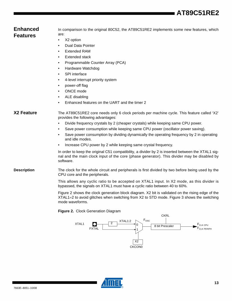
Figure 2 shows the clock generation block diagram. X2 bit is validated on the rising edge of theXTAL1÷2 to avoid glitches when switching from X2 to STD mode. Figure 3 shows the switchingmode waveforms.
Figure 2. Clock Generation Diagram
XTAL1 2
CKCON0
X2
8 bit Prescaler
FOSC
FXTAL0
1
XTAL1:2FCLK CPU
FCLK PERIPH
CKRL
137663E–8051–10/08
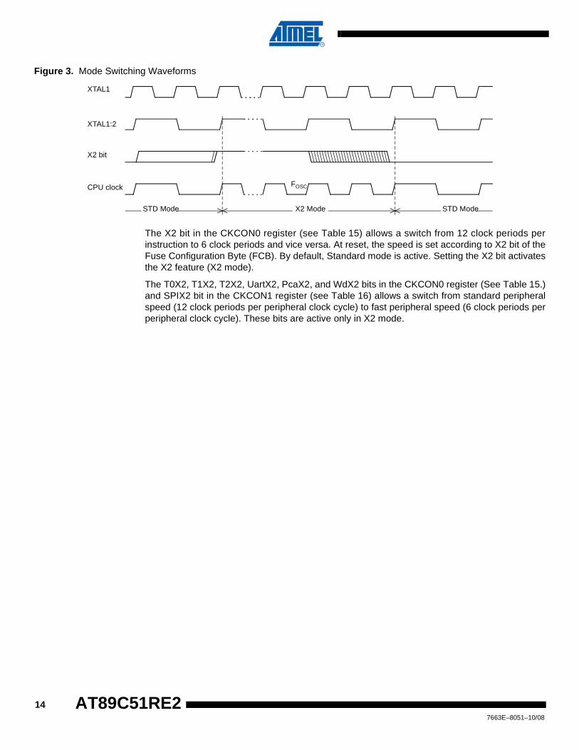
Figure 3. Mode Switching Waveforms
The X2 bit in the CKCON0 register (see Table 15) allows a switch from 12 clock periods perinstruction to 6 clock periods and vice versa. At reset, the speed is set according to X2 bit of theFuse Configuration Byte (FCB). By default, Standard mode is active. Setting the X2 bit activatesthe X2 feature (X2 mode).
The T0X2, T1X2, T2X2, UartX2, PcaX2, and WdX2 bits in the CKCON0 register (See Table 15.)and SPIX2 bit in the CKCON1 register (see Table 16) allows a switch from standard peripheralspeed (12 clock periods per peripheral clock cycle) to fast peripheral speed (6 clock periods perperipheral clock cycle). These bits are active only in X2 mode.
XTAL1:2
XTAL1
CPU clock
X2 bit
X2 ModeSTD Mode STD Mode
FOSC
147663E–8051–10/08
AT89C51RE2
AT89C51RE2
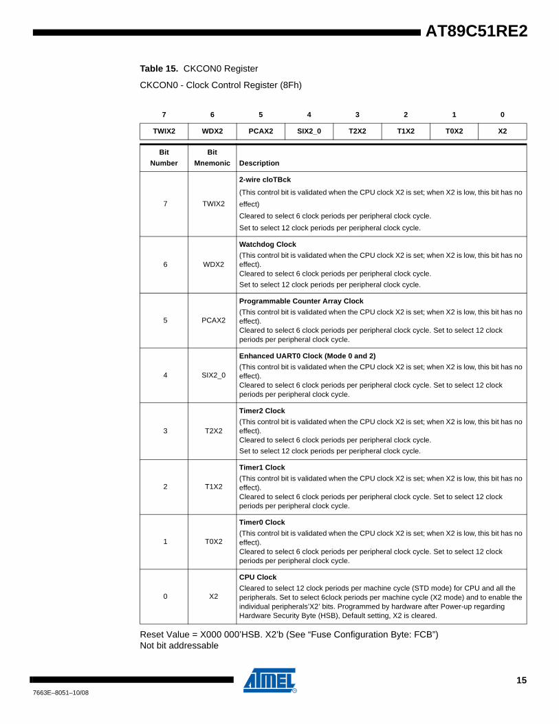
Table 15. CKCON0 Register
CKCON0 - Clock Control Register (8Fh)
Reset Value = X000 000’HSB. X2’b (See “Fuse Configuration Byte: FCB”)Not bit addressable
7 6 5 4 3 2 1 0
TWIX2 WDX2 PCAX2 SIX2_0 T2X2 T1X2 T0X2 X2
Bit
Number
Bit
Mnemonic Description
7 TWIX2
2-wire cloTBck
(This control bit is validated when the CPU clock X2 is set; when X2 is low, this bit has no
effect)
Cleared to select 6 clock periods per peripheral clock cycle.
Set to select 12 clock periods per peripheral clock cycle.
6 WDX2
Watchdog Clock
(This control bit is validated when the CPU clock X2 is set; when X2 is low, this bit has no effect).Cleared to select 6 clock periods per peripheral clock cycle.
Set to select 12 clock periods per peripheral clock cycle.
5 PCAX2
Programmable Counter Array Clock
(This control bit is validated when the CPU clock X2 is set; when X2 is low, this bit has no effect).Cleared to select 6 clock periods per peripheral clock cycle. Set to select 12 clock periods per peripheral clock cycle.
4 SIX2_0
Enhanced UART0 Clock (Mode 0 and 2)
(This control bit is validated when the CPU clock X2 is set; when X2 is low, this bit has no effect).Cleared to select 6 clock periods per peripheral clock cycle. Set to select 12 clock periods per peripheral clock cycle.
3 T2X2
Timer2 Clock
(This control bit is validated when the CPU clock X2 is set; when X2 is low, this bit has no effect).Cleared to select 6 clock periods per peripheral clock cycle.
Set to select 12 clock periods per peripheral clock cycle.
2 T1X2
Timer1 Clock
(This control bit is validated when the CPU clock X2 is set; when X2 is low, this bit has no effect).Cleared to select 6 clock periods per peripheral clock cycle. Set to select 12 clock periods per peripheral clock cycle.
1 T0X2
Timer0 Clock
(This control bit is validated when the CPU clock X2 is set; when X2 is low, this bit has no effect).Cleared to select 6 clock periods per peripheral clock cycle. Set to select 12 clock periods per peripheral clock cycle.
0 X2
CPU Clock
Cleared to select 12 clock periods per machine cycle (STD mode) for CPU and all the peripherals. Set to select 6clock periods per machine cycle (X2 mode) and to enable the individual peripherals’X2’ bits. Programmed by hardware after Power-up regarding Hardware Security Byte (HSB), Default setting, X2 is cleared.
157663E–8051–10/08

167663E–8051–10/08
AT89C51RE2
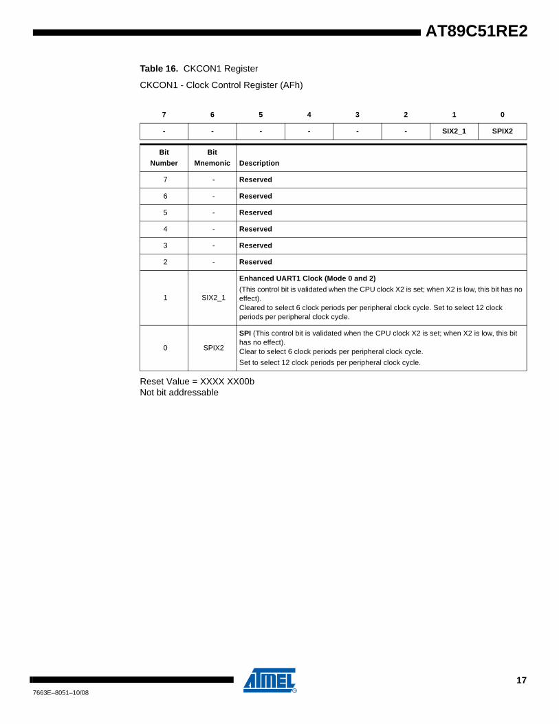
AT89C51RE2
Table 16. CKCON1 Register
CKCON1 - Clock Control Register (AFh)
Reset Value = XXXX XX00bNot bit addressable
7 6 5 4 3 2 1 0
- - - - - - SIX2_1 SPIX2
Bit
Number
Bit
Mnemonic Description
7 - Reserved
6 - Reserved
5 - Reserved
4 - Reserved
3 - Reserved
2 - Reserved
1 SIX2_1
Enhanced UART1 Clock (Mode 0 and 2)
(This control bit is validated when the CPU clock X2 is set; when X2 is low, this bit has no effect).Cleared to select 6 clock periods per peripheral clock cycle. Set to select 12 clock periods per peripheral clock cycle.
0 SPIX2
SPI (This control bit is validated when the CPU clock X2 is set; when X2 is low, this bit has no effect).Clear to select 6 clock periods per peripheral clock cycle.
Set to select 12 clock periods per peripheral clock cycle.
177663E–8051–10/08
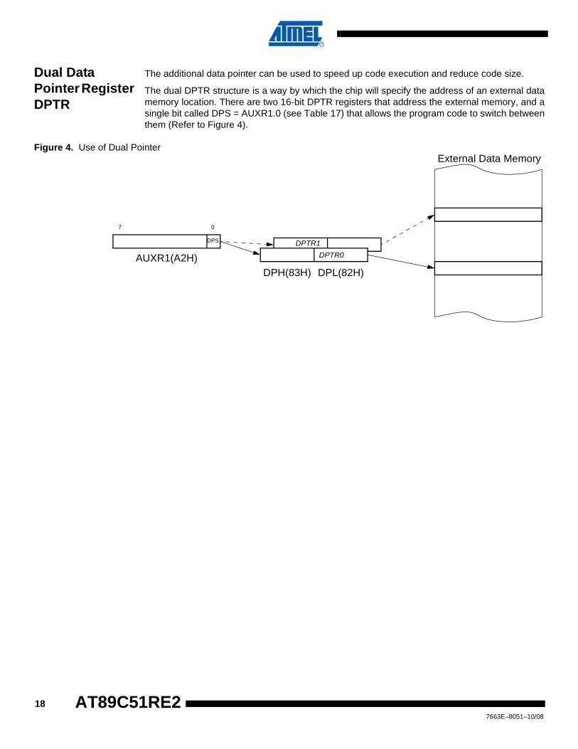
Dual Data Pointer Register DPTR
The additional data pointer can be used to speed up code execution and reduce code size.
The dual DPTR structure is a way by which the chip will specify the address of an external datamemory location. There are two 16-bit DPTR registers that address the external memory, and asingle bit called DPS = AUXR1.0 (see Table 17) that allows the program code to switch betweenthem (Refer to Figure 4).
Figure 4. Use of Dual PointerExternal Data Memory
AUXR1(A2H)
DPS
DPH(83H) DPL(82H)
07
DPTR0
DPTR1
187663E–8051–10/08
AT89C51RE2
AT89C51RE2
Table 17. AUXR1 register
AUXR1- Auxiliary Register 1(0A2h)
Reset Value: XX0X XX0X0b
Not bit addressableNote: *Bit 2 stuck at 0; this allows to use INC AUXR1 to toggle DPS without changing GF3.
ASSEMBLY LANGUAGE
; Block move using dual data pointers ; Modifies DPTR0, DPTR1, A and PSW ; note: DPS exits opposite of entry state ; unless an extra INC AUXR1 is added ; 00A2 AUXR1 EQU 0A2H ; 0000 909000MOV DPTR,#SOURCE ; address of SOURCE 0003 05A2 INC AUXR1 ; switch data pointers 0005 90A000 MOV DPTR,#DEST ; address of DEST 0008 LOOP: 0008 05A2 INC AUXR1 ; switch data pointers 000A E0 MOVX A,@DPTR ; get a byte from SOURCE 000B A3 INC DPTR ; increment SOURCE address 000C 05A2 INC AUXR1 ; switch data pointers 000E F0 MOVX @DPTR,A ; write the byte to DEST 000F A3 INC DPTR ; increment DEST address
7 6 5 4 3 2 1 0
EES SP9 U2 - GF2 0 - DPS
Bit
Number
Bit
Mnemonic Description
7 EES
Enable Extended StackThis bit allows the selection of the stack extended mode.
Set to enable the extended stack
Clear to disable the extended stack (default value)
6 SP9
Stack Pointer 9th BitThis bit has no effect when the EES bit is cleared.
Set when the stack pointer belongs to the XRAM memory space
Cleared when the stack pointer belongs to the 256bytes of internal RAM.
5 U2
P4 bit addressable
Clear to map SCON_1 register at C0h sfr address
Set to map P4 port register at C0h address.
4 -Reserved
The value read from this bit is indeterminate. Do not set this bit.
3 GF2 This bit is a general purpose user flag. *
2 0 Always cleared.
1 -Reserved
The value read from this bit is indeterminate. Do not set this bit.
0 DPSData Pointer Selection
Cleared to select DPTR0.Set to select DPTR1.
197663E–8051–10/08

0010 70F6JNZ LOOP ; check for 0 terminator 0012 05A2 INC AUXR1 ; (optional) restore DPS
INC is a short (2 bytes) and fast (12 clocks) way to manipulate the DPS bit in the AUXR1 SFR.However, note that the INC instruction does not directly force the DPS bit to a particular state,but simply toggles it. In simple routines, such as the block move example, only the fact that DPSis toggled in the proper sequence matters, not its actual value. In other words, the block moveroutine works the same whether DPS is '0' or '1' on entry. Observe that without the last instruc-tion (INC AUXR1), the routine will exit with DPS in the opposite state.
207663E–8051–10/08
AT89C51RE2
217663E–8051–10/08
AT89C51RE2
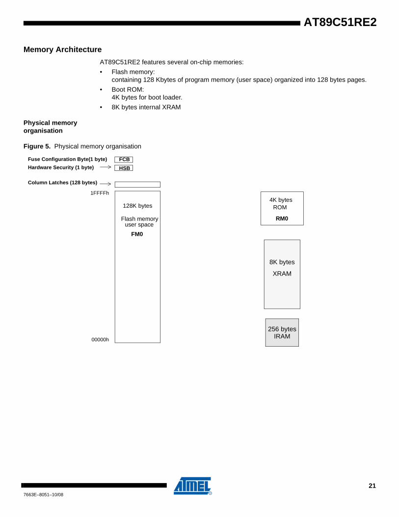
Memory Architecture
AT89C51RE2 features several on-chip memories:
• Flash memory: containing 128 Kbytes of program memory (user space) organized into 128 bytes pages.
• Boot ROM:4K bytes for boot loader.
• 8K bytes internal XRAM
Physical memory organisation
Figure 5. Physical memory organisation
128K bytes
Flash memory
FM0
Hardware Security (1 byte)
Column Latches (128 bytes)
user space
4K bytesROM
1FFFFh
00000h
RM0
Fuse Configuration Byte(1 byte) FCB
HSB
256 bytesIRAM
XRAM
8K bytes
Expanded RAM (XRAM)
The AT89C51RE2 provides additional Bytes of random access memory (RAM) space forincreased data parameter handling and high level language usage.
AT89C51RE2 devices have expanded RAM in external data space configurable up to 8192bytes(see Table 18.).
The AT89C51RE2 has internal data memory that is mapped into four separate segments.
The four segments are:
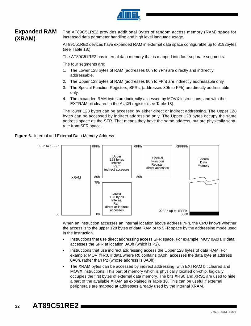
1. The Lower 128 bytes of RAM (addresses 00h to 7Fh) are directly and indirectly addressable.
2. The Upper 128 bytes of RAM (addresses 80h to FFh) are indirectly addressable only.
3. The Special Function Registers, SFRs, (addresses 80h to FFh) are directly addressable only.
4. The expanded RAM bytes are indirectly accessed by MOVX instructions, and with the EXTRAM bit cleared in the AUXR register (see Table 18).
The lower 128 bytes can be accessed by either direct or indirect addressing. The Upper 128bytes can be accessed by indirect addressing only. The Upper 128 bytes occupy the sameaddress space as the SFR. That means they have the same address, but are physically sepa-rate from SFR space.
Figure 6. Internal and External Data Memory Address
When an instruction accesses an internal location above address 7Fh, the CPU knows whetherthe access is to the upper 128 bytes of data RAM or to SFR space by the addressing mode usedin the instruction.
• Instructions that use direct addressing access SFR space. For example: MOV 0A0H, # data, accesses the SFR at location 0A0h (which is P2).
• Instructions that use indirect addressing access the Upper 128 bytes of data RAM. For example: MOV @R0, # data where R0 contains 0A0h, accesses the data byte at address 0A0h, rather than P2 (whose address is 0A0h).
• The XRAM bytes can be accessed by indirect addressing, with EXTRAM bit cleared and MOVX instructions. This part of memory which is physically located on-chip, logically occupies the first bytes of external data memory. The bits XRS0 and XRS1 are used to hide a part of the available XRAM as explained in Table 18. This can be useful if external peripherals are mapped at addresses already used by the internal XRAM.
XRAM
Upper128 bytesInternal
Ram
Lower128 bytesInternal
Ram
SpecialFunctionRegister
80h 80h
00
0FFh to 1FFFh 0FFh
00
0FFh
ExternalData
Memory
000000FFh up to 1FFFh
0FFFFh
indirect accesses direct accesses
direct or indirectaccesses
7Fh
227663E–8051–10/08
AT89C51RE2
AT89C51RE2
• With EXTRAM = 0, the XRAM is indirectly addressed, using the MOVX instruction in combination with any of the registers R0, R1 of the selected bank or DPTR. An access to XRAM will not affect ports P0, P2, P3.6 (WR) and P3.7 (RD). For example, with EXTRAM = 0, MOVX @R0, # data where R0 contains 0A0H, accesses the XRAM at address 0A0H rather than external memory. An access to external data memory locations higher than the accessible size of the XRAM will be performed with the MOVX DPTR instructions in the same way as in the standard 80C51, with P0 and P2 as data/address busses, and P3.6 and P3.7 as write and read timing signals. Accesses to XRAM above 0FFH can only be done by the use of DPTR.
• With EXTRAM = 1, MOVX @Ri and MOVX @DPTR will be similar to the standard 80C51.MOVX @ Ri will provide an eight-bit address multiplexed with data on Port0 and any output port pins can be used to output higher order address bits. This is to provide the external paging capability. MOVX @DPTR will generate a sixteen-bit address. Port2 outputs the high-order eight address bits (the contents of DPH) while Port0 multiplexes the low-order eight address bits (DPL) with data. MOVX @ Ri and MOVX @DPTR will generate either read or write signals on P3.6 (WR) and P3.7 (RD).
The stack pointer (SP) may be located anywhere in the 256 bytes RAM (lower and upper RAM)internal data memory. The stack may be located in the 256 lower bytes of the XRAM by activat-ing the extended stack mode (see EES bit in AUXR1).
The M0 bit allows to stretch the XRAM timings; if M0 is set, the read and write pulses areextended from 6 to 30 clock periods. This is useful to access external slow peripherals.
237663E–8051–10/08

Registers Table 18. AUXR Register
AUXR - Auxiliary Register (8Eh)
Reset Value = XX01 1100bNot bit addressable
7 6 5 4 3 2 1 0
- - M0 XRS2 XRS1 XRS0 EXTRAM AO
Bit
Number
Bit
Mnemonic Description
7 -Reserved
The value read from this bit is indeterminate. Do not set this bit.
6 -Reserved
The value read from this bit is indeterminate. Do not set this bit.
5 M0
Pulse length
Cleared to stretch MOVX control: the RD/ and the WR/ pulse length is 6 clock periods (default).
Set to stretch MOVX control: the RD/ and the WR/ pulse length is 30 clock periods.
4-2 XRS2:0
XRAM Size
XRS2 XRS1 XRS0 XRAM size0 0 0 256 bytes
0 0 1 512 bytes
0 1 0 768 bytes
0 1 1 1024 bytes
1 0 0 1792 bytes
1 0 1 2048 bytes
1 1 0 4096 bytes
1 1 1 8192 bytes (default)
1 EXTRAM
EXTRAM bitCleared to access internal XRAM using movx @ Ri/ @ DPTR.
Set to access external memory.
Programmed by hardware after Power-up regarding Hardware Security Byte (HSB), default setting, XRAM selected.
0 AO
ALE Output bitCleared, ALE is emitted at a constant rate of 1/6 the oscillator frequency (or 1/3 if X2 mode is used). (default) Set, ALE is active only during a MOVX or MOVC instruction is used.
247663E–8051–10/08
AT89C51RE2
AT89C51RE2
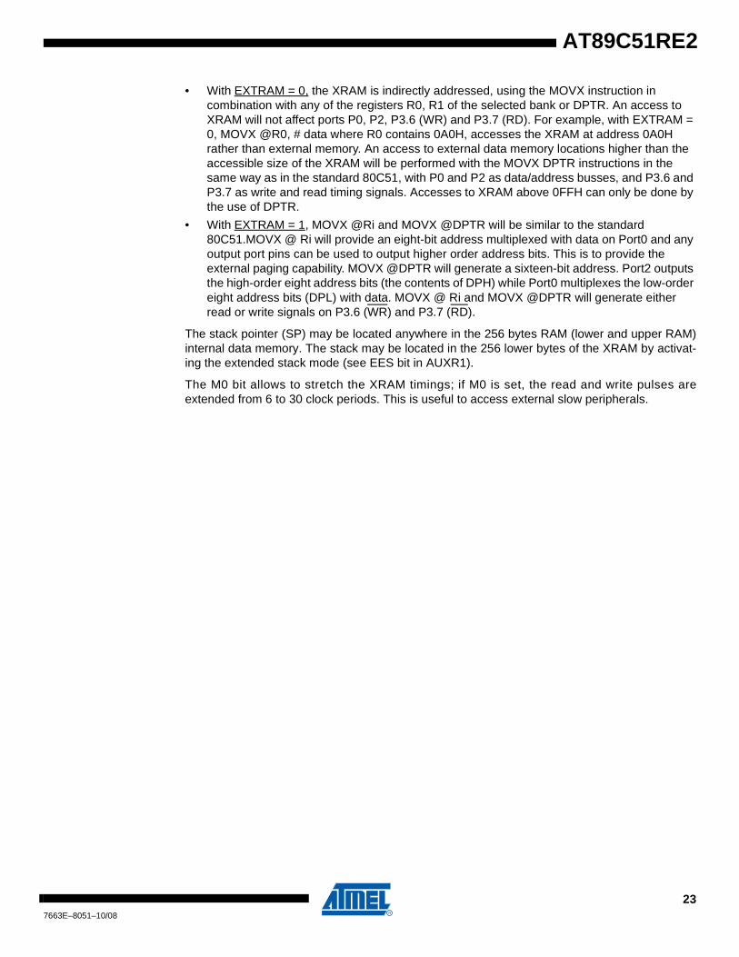
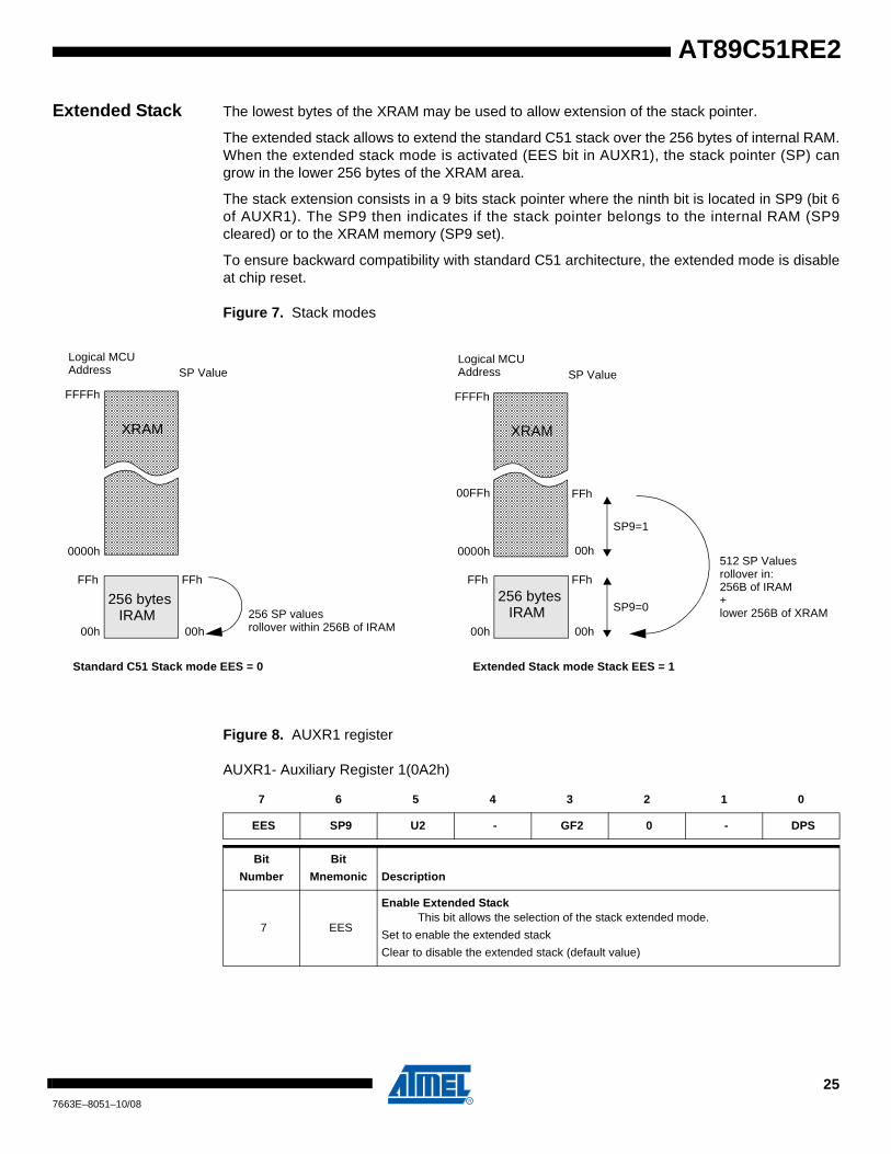
Extended Stack The lowest bytes of the XRAM may be used to allow extension of the stack pointer.
The extended stack allows to extend the standard C51 stack over the 256 bytes of internal RAM.When the extended stack mode is activated (EES bit in AUXR1), the stack pointer (SP) cangrow in the lower 256 bytes of the XRAM area.
The stack extension consists in a 9 bits stack pointer where the ninth bit is located in SP9 (bit 6of AUXR1). The SP9 then indicates if the stack pointer belongs to the internal RAM (SP9cleared) or to the XRAM memory (SP9 set).
To ensure backward compatibility with standard C51 architecture, the extended mode is disableat chip reset.
Figure 7. Stack modes
Figure 8. AUXR1 register
AUXR1- Auxiliary Register 1(0A2h)
00h
FFh
0000h
FFFFh
256 bytes IRAM
00h
FFh
Logical MCUAddress
256 SP valuesrollover within 256B of IRAM 00h
FFh
0000h
256 bytes IRAM
00h
FFh
512 SP Valuesrollover in:
00FFh
00h
FFh
256B of IRAM +lower 256B of XRAM
XRAM
SP Value
FFFFh
Logical MCUAddress
XRAM
SP Value
Standard C51 Stack mode EES = 0 Extended Stack mode Stack EES = 1
SP9=1
SP9=0
7 6 5 4 3 2 1 0
EES SP9 U2 - GF2 0 - DPS
Bit
Number
Bit
Mnemonic Description
7 EES
Enable Extended StackThis bit allows the selection of the stack extended mode.
Set to enable the extended stack
Clear to disable the extended stack (default value)
257663E–8051–10/08
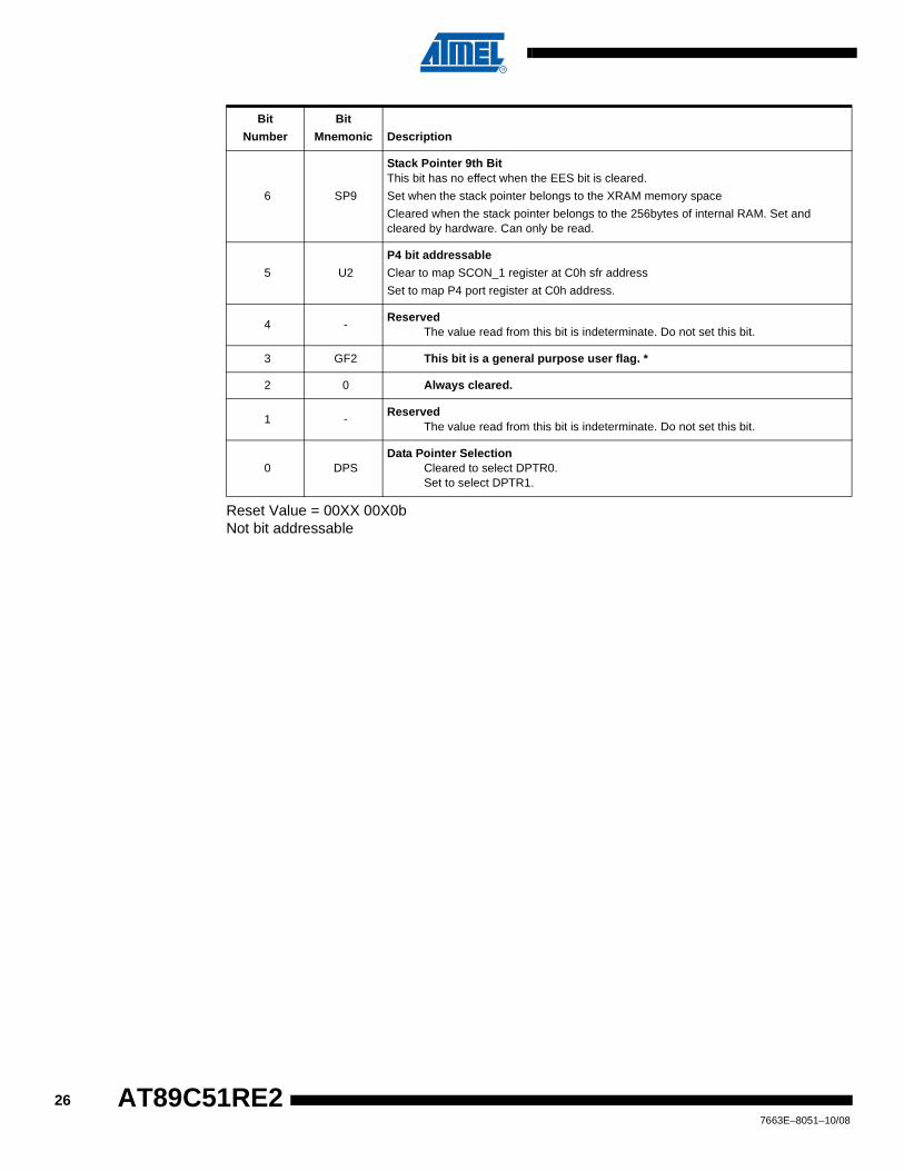
Reset Value = 00XX 00X0bNot bit addressable
6 SP9
Stack Pointer 9th BitThis bit has no effect when the EES bit is cleared.
Set when the stack pointer belongs to the XRAM memory space
Cleared when the stack pointer belongs to the 256bytes of internal RAM. Set and cleared by hardware. Can only be read.
5 U2
P4 bit addressable
Clear to map SCON_1 register at C0h sfr address
Set to map P4 port register at C0h address.
4 -Reserved
The value read from this bit is indeterminate. Do not set this bit.
3 GF2 This bit is a general purpose user flag. *
2 0 Always cleared.
1 -Reserved
The value read from this bit is indeterminate. Do not set this bit.
0 DPSData Pointer Selection
Cleared to select DPTR0.Set to select DPTR1.
Bit
Number
Bit
Mnemonic Description
267663E–8051–10/08
AT89C51RE2
AT89C51RE2
Flash Memory
General Description
The Flash memory increases EPROM and ROM functionality with in-circuit electrical erasureand programming. It contains 128K bytes of program memory organized in 1024 pages of 128bytes. This memory is both parallel and serial In-System Programmable (ISP). ISP allowsdevices to alter their own program memory in the actual end product under software control. Adefault serial loader (bootloader) program allows ISP of the Flash.
The programming does not require external high programming voltage. The necessary high pro-gramming voltage is generated on-chip using the standard VCC pins of the microcontroller.
Features • Flash internal program memory.
• Boot vector allows user provided Flash loader code to reside anywhere in the Flash memory space. This configuration provides flexibility to the user.
• Default loader in Boot Flash allows programming via the serial port without the need of a user provided loader.
• Up to 64K byte external program memory if the internal program memory is disabled (EA = 0).
• Programming and erase voltage with standard 5V or 3V VCC supply.
Flash memory organization
AT89C51RE2 features several on-chip memories:
• Flash memory FM0: containing 128 Kbytes of program memory (user space) organized into 128 bytes pages.
• Boot ROM RM0:4K bytes for boot loader.
• 8K bytes internal XRAM
277663E–8051–10/08
Physical memory organisation
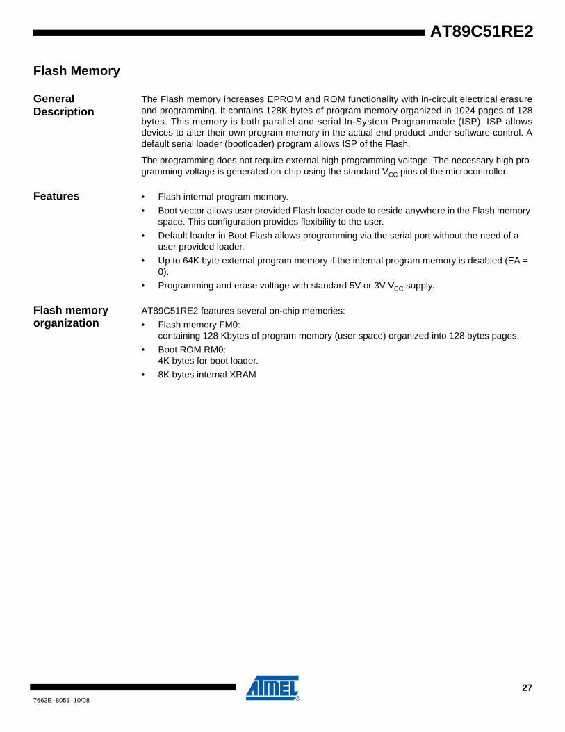
Figure 9. Physical memory organisation
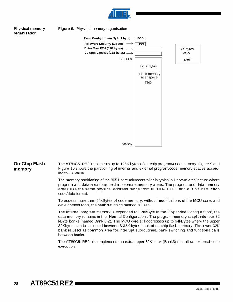
On-Chip Flash memory
The AT89C51RE2 implements up to 128K bytes of on-chip program/code memory. Figure 9 andFigure 10 shows the partitioning of internal and external program/code memory spaces accord-ing to EA value.
The memory partitioning of the 8051 core microcontroller is typical a Harvard architecture whereprogram and data areas are held in separate memory areas. The program and data memoryareas use the same physical address range from 0000H-FFFFH and a 8 bit instructioncode/data format.
To access more than 64kBytes of code memory, without modifications of the MCU core, anddevelopment tools, the bank switching method is used.
The internal program memory is expanded to 128kByte in the ´Expanded Configuration’, thedata memory remains in the ´Normal Configuration´. The program memory is split into four 32kByte banks (named Bank 0-2). The MCU core still addresses up to 64kBytes where the upper32Kbytes can be selected between 3 32K bytes bank of on-chip flash memory. The lower 32Kbank is used as common area for interrupt subroutines, bank switching and functions callsbetween banks.
The AT89C51RE2 also implements an extra upper 32K bank (Bank3) that allows external codeexecution.
128K bytes
Flash memory
FM0
Hardware Security (1 byte)
Column Latches (128 bytes)
user space
Extra Row FM0 (128 bytes) 4K bytesROM
1FFFFh
00000h
RM0
Fuse Configuration Byte(1 byte) FCB
HSB
287663E–8051–10/08
AT89C51RE2

AT89C51RE2
Figure 10. Program/Code Memory Organization EA=1
0000h
7FFFh
8000h
FFFFh
8000h
FFFFh
8000h
FFFFh
8000h
FFFFh
32KCommon
upper 32KBank 0
upper 32KBank 1
upper 32KBank 2
upper 32KBank 3
OptionalExternalMemory
On-Chip flash code memory
External code memory00000h
07FFFh
08000h
0FFFFh
10000h
17FFFh
18000h
1FFFFh
Logical MCUAddress
Physical FlashAddress
Logical MCUAddress
Logical MCUAddress
Physical FlashAddress
Physical FlashAddress
Logical MCUAddress
297663E–8051–10/08
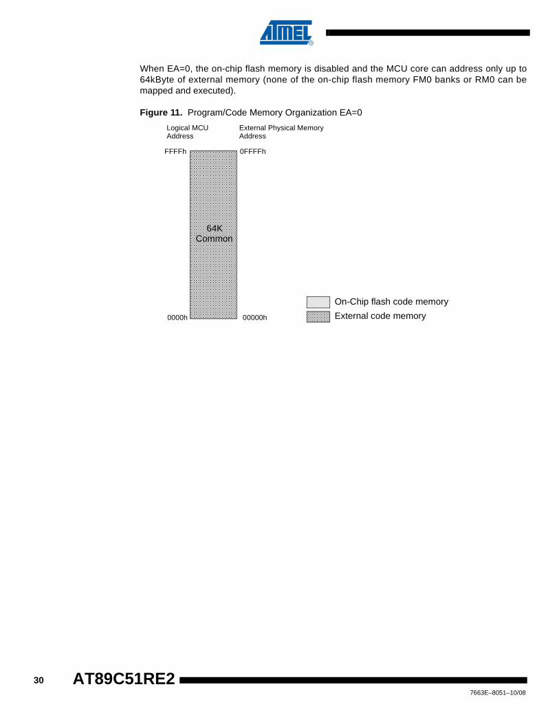
When EA=0, the on-chip flash memory is disabled and the MCU core can address only up to64kByte of external memory (none of the on-chip flash memory FM0 banks or RM0 can bemapped and executed).
Figure 11. Program/Code Memory Organization EA=0
0000h
FFFFh
64KCommon
On-Chip flash code memory
External code memory00000h
0FFFFh
Logical MCUAddress
External Physical MemoryAddress
307663E–8051–10/08
AT89C51RE2

AT89C51RE2
On-Chip ROM bootloader
The On-chip ROM bootloader (RM0) is enable only for ISP operations after reset (bootloaderexecution). The RM0 memory area belongs to a logical addressable memory space called ‘BankBoot’.
RM0 cannot be activated from the On-chip flash memory. It means that it is not possible acti-vate the Bank Boot area by software (it prevents any RM0 execution and flash corruption fromthe user application).
RM0 logical area consists in an independent code execution memory area of 4K bytes startingat logical 0x0000 address (it allows the use of the interrupts in the bootloader execution).
0000h
7FFFh
8000h
FFFFh
8000h
FFFFh
8000h
FFFFh
8000h
FFFFh
Bank 0
On-Chip flash code memory
External code memory00000h
07FFFh
08000h
0FFFFh
10000h
17FFFh
18000h
1FFFFh
Logical MCUAddress
PhysicalAddress
Logical MCUAddress
Logical MCUAddress
PhysicalAddress
PhysicalAddress
Logical MCUAddress
Bank 1 Bank 2 Bank 3
Logical MCUAddress
ROMAddress
Bank BOOT
(Ext)
0000h
On-Chip ROM memory (RM0) 1000h
0000h
1000h
317663E–8051–10/08
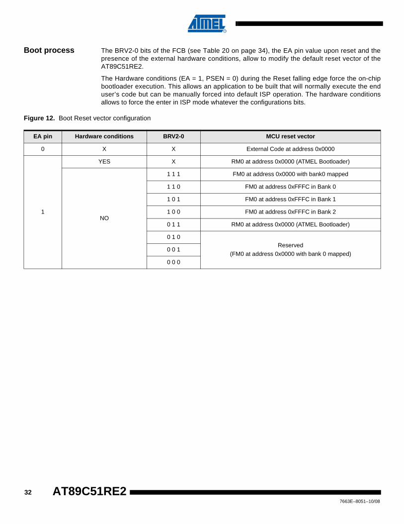
Boot process The BRV2-0 bits of the FCB (see Table 20 on page 34), the EA pin value upon reset and thepresence of the external hardware conditions, allow to modify the default reset vector of theAT89C51RE2.
The Hardware conditions (EA = 1, PSEN = 0) during the Reset falling edge force the on-chipbootloader execution. This allows an application to be built that will normally execute the enduser’s code but can be manually forced into default ISP operation. The hardware conditionsallows to force the enter in ISP mode whatever the configurations bits.
Figure 12. Boot Reset vector configuration
EA pin Hardware conditions BRV2-0 MCU reset vector
0 X X External Code at address 0x0000
1
YES X RM0 at address 0x0000 (ATMEL Bootloader)
NO
1 1 1 FM0 at address 0x0000 with bank0 mapped
1 1 0 FM0 at address 0xFFFC in Bank 0
1 0 1 FM0 at address 0xFFFC in Bank 1
1 0 0 FM0 at address 0xFFFC in Bank 2
0 1 1 RM0 at address 0x0000 (ATMEL Bootloader)
0 1 0Reserved
(FM0 at address 0x0000 with bank 0 mapped)0 0 1
0 0 0
327663E–8051–10/08
AT89C51RE2
AT89C51RE2
FM0 Memory Architecture
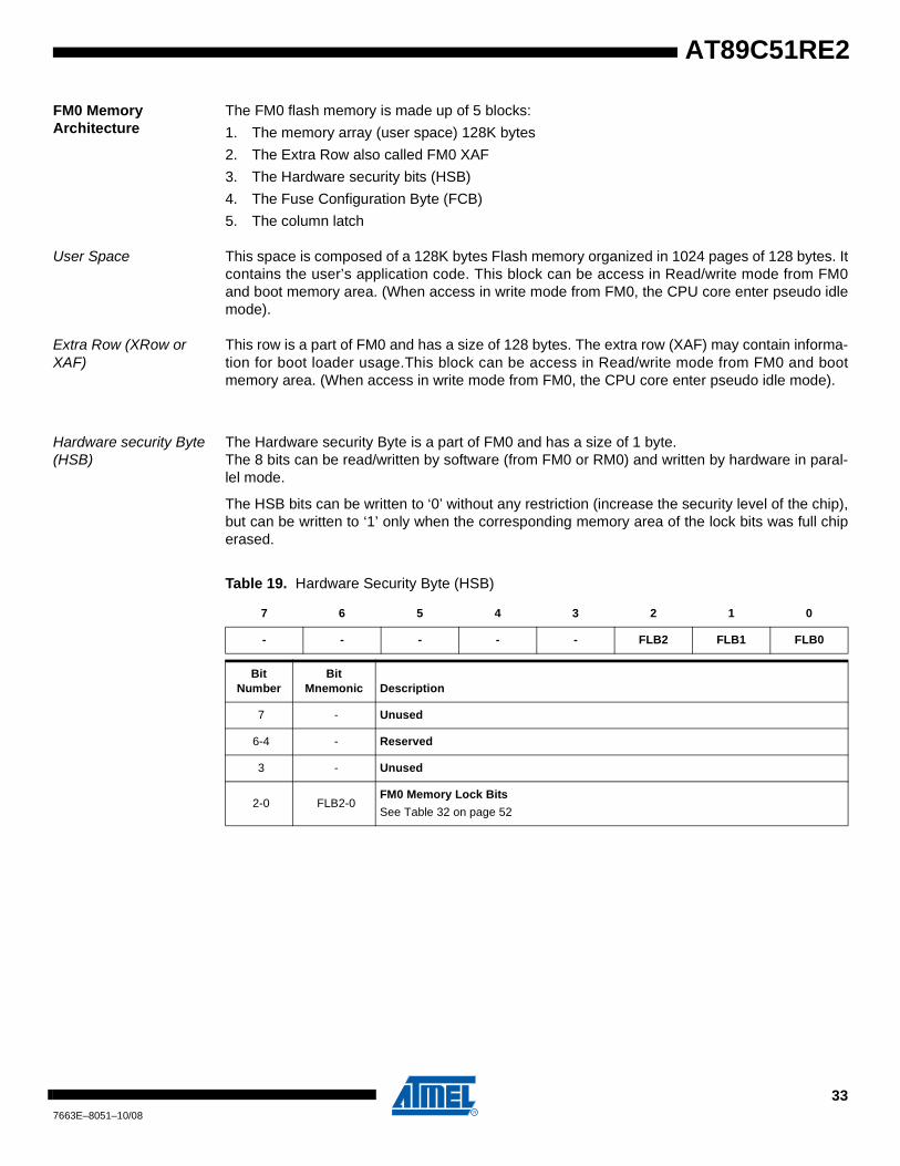
The FM0 flash memory is made up of 5 blocks:
1. The memory array (user space) 128K bytes
2. The Extra Row also called FM0 XAF
3. The Hardware security bits (HSB)
4. The Fuse Configuration Byte (FCB)
5. The column latch
User Space This space is composed of a 128K bytes Flash memory organized in 1024 pages of 128 bytes. Itcontains the user’s application code. This block can be access in Read/write mode from FM0and boot memory area. (When access in write mode from FM0, the CPU core enter pseudo idlemode).
Extra Row (XRow or XAF)
This row is a part of FM0 and has a size of 128 bytes. The extra row (XAF) may contain informa-tion for boot loader usage.This block can be access in Read/write mode from FM0 and bootmemory area. (When access in write mode from FM0, the CPU core enter pseudo idle mode).
Hardware security Byte (HSB)
The Hardware security Byte is a part of FM0 and has a size of 1 byte.The 8 bits can be read/written by software (from FM0 or RM0) and written by hardware in paral-lel mode.
The HSB bits can be written to ‘0’ without any restriction (increase the security level of the chip),but can be written to ‘1’ only when the corresponding memory area of the lock bits was full chiperased.
Table 19. Hardware Security Byte (HSB)
7 6 5 4 3 2 1 0
- - - - - FLB2 FLB1 FLB0
Bit Number
Bit Mnemonic Description
7 - Unused
6-4 - Reserved
3 - Unused
2-0 FLB2-0FM0 Memory Lock Bits
See Table 32 on page 52
337663E–8051–10/08
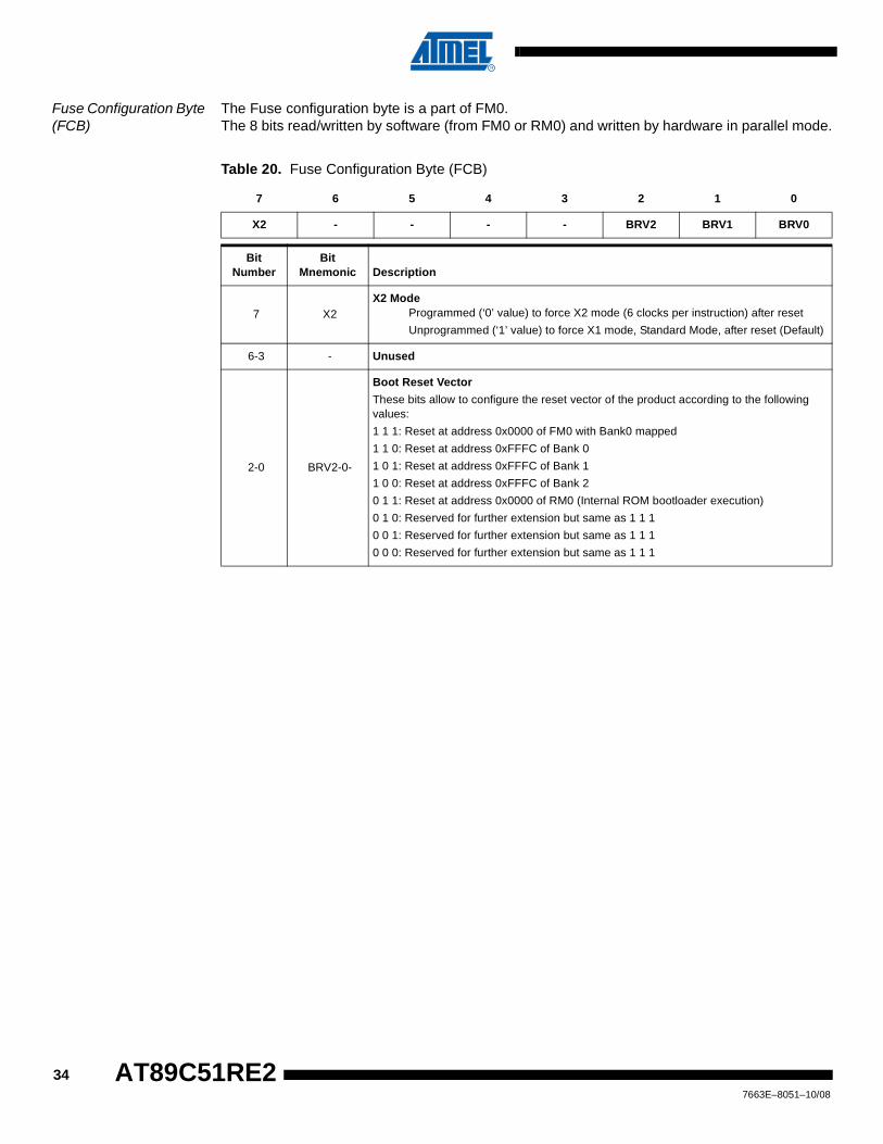
Fuse Configuration Byte (FCB)
The Fuse configuration byte is a part of FM0.The 8 bits read/written by software (from FM0 or RM0) and written by hardware in parallel mode.
Table 20. Fuse Configuration Byte (FCB)
7 6 5 4 3 2 1 0
X2 - - - - BRV2 BRV1 BRV0
Bit Number
Bit Mnemonic Description
7 X2X2 Mode
Programmed (‘0’ value) to force X2 mode (6 clocks per instruction) after reset
Unprogrammed (‘1’ value) to force X1 mode, Standard Mode, after reset (Default)
6-3 - Unused
2-0 BRV2-0-
Boot Reset Vector
These bits allow to configure the reset vector of the product according to the following values:
1 1 1: Reset at address 0x0000 of FM0 with Bank0 mapped
1 1 0: Reset at address 0xFFFC of Bank 0
1 0 1: Reset at address 0xFFFC of Bank 1
1 0 0: Reset at address 0xFFFC of Bank 2
0 1 1: Reset at address 0x0000 of RM0 (Internal ROM bootloader execution)
0 1 0: Reserved for further extension but same as 1 1 1
0 0 1: Reserved for further extension but same as 1 1 1
0 0 0: Reserved for further extension but same as 1 1 1
347663E–8051–10/08
AT89C51RE2
AT89C51RE2
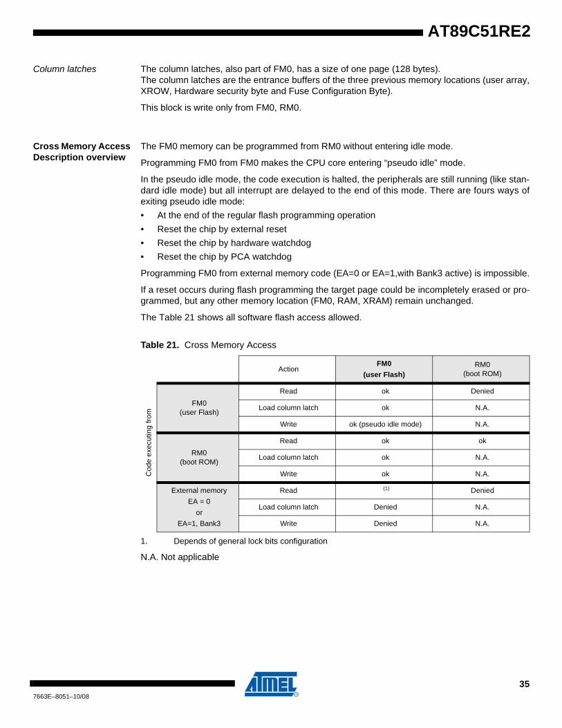
Column latches The column latches, also part of FM0, has a size of one page (128 bytes).The column latches are the entrance buffers of the three previous memory locations (user array,XROW, Hardware security byte and Fuse Configuration Byte).
This block is write only from FM0, RM0.
Cross Memory Access Description overview
The FM0 memory can be programmed from RM0 without entering idle mode.
Programming FM0 from FM0 makes the CPU core entering “pseudo idle” mode.
In the pseudo idle mode, the code execution is halted, the peripherals are still running (like stan-dard idle mode) but all interrupt are delayed to the end of this mode. There are fours ways ofexiting pseudo idle mode:
• At the end of the regular flash programming operation
• Reset the chip by external reset
• Reset the chip by hardware watchdog
• Reset the chip by PCA watchdog
Programming FM0 from external memory code (EA=0 or EA=1,with Bank3 active) is impossible.
If a reset occurs during flash programming the target page could be incompletely erased or pro-grammed, but any other memory location (FM0, RAM, XRAM) remain unchanged.
The Table 21 shows all software flash access allowed.
Table 21. Cross Memory Access
Cod
e ex
ecut
ing
from
ActionFM0
(user Flash)RM0
(boot ROM)
FM0(user Flash)
Read ok Denied
Load column latch ok N.A.
Write ok (pseudo idle mode) N.A.
RM0(boot ROM)
Read ok ok
Load column latch ok N.A.
Write ok N.A.
External memory
EA = 0
or
EA=1, Bank3
Read (1)
1. Depends of general lock bits configuration
N.A. Not applicable
Denied
Load column latch Denied N.A.
Write Denied N.A.
357663E–8051–10/08
Access and Operations Descriptions
FM0 FLASH Registers
The CPU interfaces to the flash memory through the FCON register, AUXR1 register and FSTAregister.
These registers are used to map the columns latch, HSB, FCB and extra row in the working dataor code space.
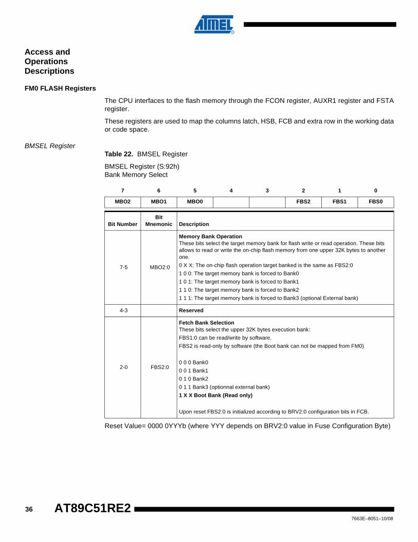
BMSEL RegisterTable 22. BMSEL Register
BMSEL Register (S:92h)Bank Memory Select
Reset Value= 0000 0YYYb (where YYY depends on BRV2:0 value in Fuse Configuration Byte)
7 6 5 4 3 2 1 0
MBO2 MBO1 MBO0 FBS2 FBS1 FBS0
Bit NumberBit
Mnemonic Description
7-5 MBO2:0
Memory Bank OperationThese bits select the target memory bank for flash write or read operation. These bits allows to read or write the on-chip flash memory from one upper 32K bytes to another one.
0 X X: The on-chip flash operation target banked is the same as FBS2:0
1 0 0: The target memory bank is forced to Bank0
1 0 1: The target memory bank is forced to Bank1
1 1 0: The target memory bank is forced to Bank2
1 1 1: The target memory bank is forced to Bank3 (optional External bank)
4-3 Reserved
2-0 FBS2:0
Fetch Bank SelectionThese bits select the upper 32K bytes execution bank:
FBS1:0 can be read/write by software.
FBS2 is read-only by software (the Boot bank can not be mapped from FM0)
0 0 0 Bank0
0 0 1 Bank1
0 1 0 Bank2
0 1 1 Bank3 (optionnal external bank)
1 X X Boot Bank (Read only)
Upon reset FBS2:0 is initialized according to BRV2:0 configuration bits in FCB.
367663E–8051–10/08
AT89C51RE2

AT89C51RE2
FCON RegisterTable 23. FCON Register
FCON Register (S:D1h)Flash Control Register
Reset Value= 0000 0000b
7 6 5 4 3 2 1 0
FPL3 FPL2 FPL1 FPL0 FPS FMOD2 FMOD1 FMOD0
Bit NumberBit
Mnemonic Description
7-4 FPL3:0Programming Launch Command BitsWrite 5Xh followed by AXh to launch the programming according to FMOD2:0. (see Table 26.)
3 FPS
Flash Map Program Space When this bit is set:
The MOVX @DPTR, A instruction writes in the columns latches space
When this bit is cleared:
The MOVX @DPTR, A instruction writes in the regular XDATA memory space
2-0 FMOD2:0Flash ModeThese bits allow to select the target memory area and operation on FM0
See Table 25.
377663E–8051–10/08
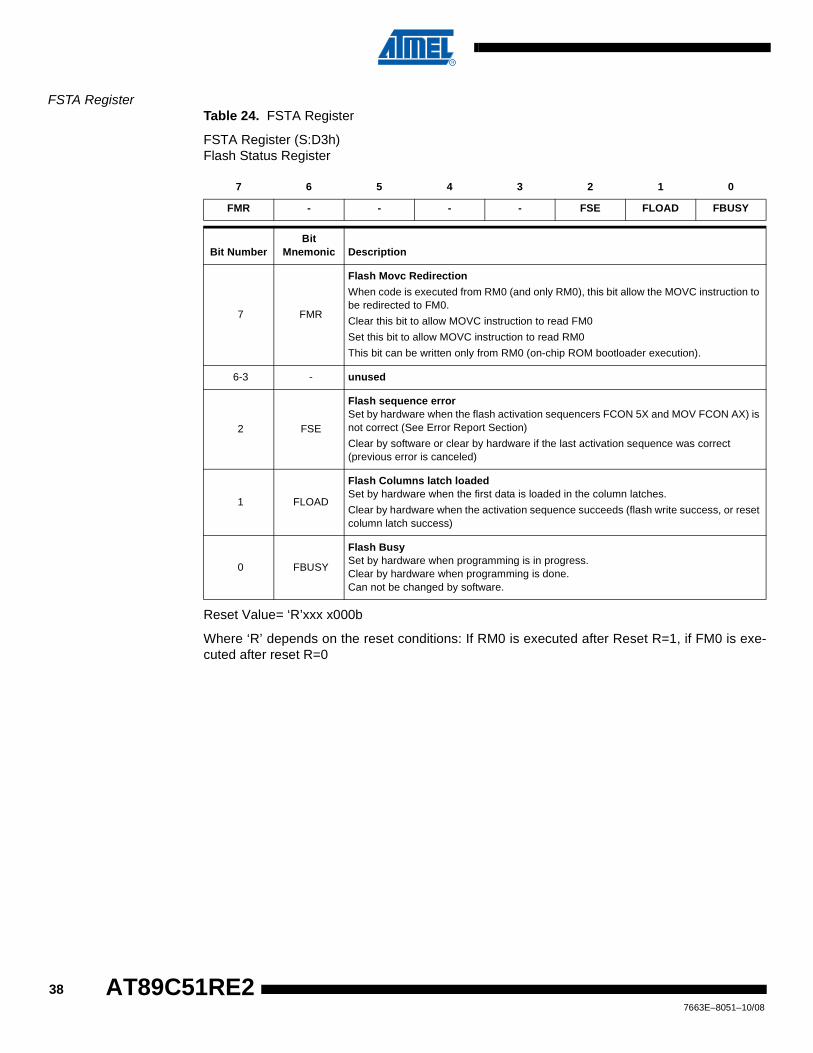
FSTA RegisterTable 24. FSTA Register
FSTA Register (S:D3h)Flash Status Register
Reset Value= ‘R’xxx x000b
Where ‘R’ depends on the reset conditions: If RM0 is executed after Reset R=1, if FM0 is exe-cuted after reset R=0
7 6 5 4 3 2 1 0
FMR - - - - FSE FLOAD FBUSY
Bit NumberBit
Mnemonic Description
7 FMR
Flash Movc Redirection
When code is executed from RM0 (and only RM0), this bit allow the MOVC instruction to be redirected to FM0.
Clear this bit to allow MOVC instruction to read FM0
Set this bit to allow MOVC instruction to read RM0
This bit can be written only from RM0 (on-chip ROM bootloader execution).
6-3 - unused
2 FSE
Flash sequence errorSet by hardware when the flash activation sequencers FCON 5X and MOV FCON AX) is not correct (See Error Report Section)
Clear by software or clear by hardware if the last activation sequence was correct (previous error is canceled)
1 FLOAD
Flash Columns latch loadedSet by hardware when the first data is loaded in the column latches.
Clear by hardware when the activation sequence succeeds (flash write success, or reset column latch success)
0 FBUSY
Flash BusySet by hardware when programming is in progress.Clear by hardware when programming is done.Can not be changed by software.
387663E–8051–10/08
AT89C51RE2
AT89C51RE2
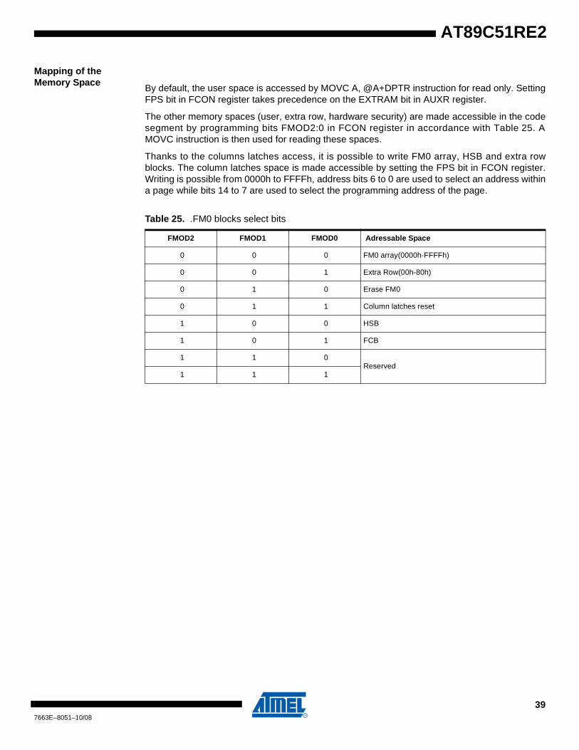
Mapping of the Memory Space
By default, the user space is accessed by MOVC A, @A+DPTR instruction for read only. SettingFPS bit in FCON register takes precedence on the EXTRAM bit in AUXR register.
The other memory spaces (user, extra row, hardware security) are made accessible in the codesegment by programming bits FMOD2:0 in FCON register in accordance with Table 25. AMOVC instruction is then used for reading these spaces.
Thanks to the columns latches access, it is possible to write FM0 array, HSB and extra rowblocks. The column latches space is made accessible by setting the FPS bit in FCON register.Writing is possible from 0000h to FFFFh, address bits 6 to 0 are used to select an address withina page while bits 14 to 7 are used to select the programming address of the page.
Table 25. .FM0 blocks select bits
FMOD2 FMOD1 FMOD0 Adressable Space
0 0 0 FM0 array(0000h-FFFFh)
0 0 1 Extra Row(00h-80h)
0 1 0 Erase FM0
0 1 1 Column latches reset
1 0 0 HSB
1 0 1 FCB
1 1 0Reserved
1 1 1
397663E–8051–10/08
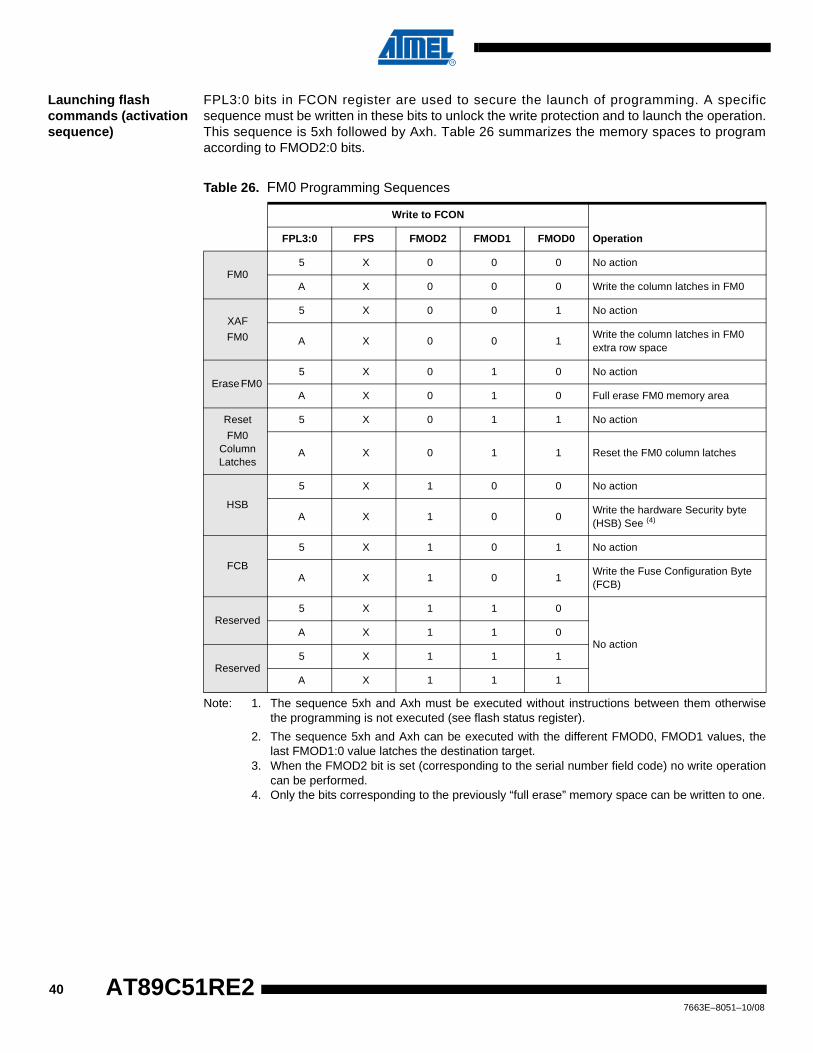
Launching flash commands (activation sequence)
FPL3:0 bits in FCON register are used to secure the launch of programming. A specificsequence must be written in these bits to unlock the write protection and to launch the operation.This sequence is 5xh followed by Axh. Table 26 summarizes the memory spaces to programaccording to FMOD2:0 bits.
Table 26. FM0 Programming Sequences
Note: 1. The sequence 5xh and Axh must be executed without instructions between them otherwisethe programming is not executed (see flash status register).
2. The sequence 5xh and Axh can be executed with the different FMOD0, FMOD1 values, thelast FMOD1:0 value latches the destination target.
3. When the FMOD2 bit is set (corresponding to the serial number field code) no write operationcan be performed.
4. Only the bits corresponding to the previously “full erase” memory space can be written to one.
Write to FCON
OperationFPL3:0 FPS FMOD2 FMOD1 FMOD0
FM05 X 0 0 0 No action
A X 0 0 0 Write the column latches in FM0
XAF
FM0
5 X 0 0 1 No action
A X 0 0 1Write the column latches in FM0 extra row space
Erase FM0 5 X 0 1 0 No action
A X 0 1 0 Full erase FM0 memory area
Reset
FM0 Column Latches
5 X 0 1 1 No action
A X 0 1 1 Reset the FM0 column latches
HSB
5 X 1 0 0 No action
A X 1 0 0Write the hardware Security byte (HSB) See (4)
FCB
5 X 1 0 1 No action
A X 1 0 1Write the Fuse Configuration Byte (FCB)
Reserved5 X 1 1 0
No actionA X 1 1 0
Reserved5 X 1 1 1
A X 1 1 1
407663E–8051–10/08
AT89C51RE2
AT89C51RE2
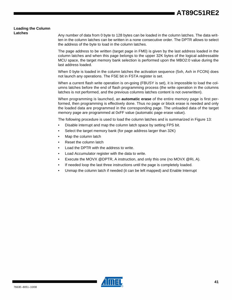
Loading the Column Latches
Any number of data from 0 byte to 128 bytes can be loaded in the column latches. The data writ-ten in the column latches can be written in a none consecutive order. The DPTR allows to selectthe address of the byte to load in the column latches.
The page address to be written (target page in FM0) is given by the last address loaded in thecolumn latches and when this page belongs to the upper 32K bytes of the logical addressableMCU space, the target memory bank selection is performed upon the MBO2:0 value during thelast address loaded.
When 0 byte is loaded in the column latches the activation sequence (5xh, Axh in FCON) doesnot launch any operations. The FSE bit in FSTA register is set.
When a current flash write operation is on-going (FBUSY is set), it is impossible to load the col-umns latches before the end of flash programming process (the write operation in the columnslatches is not performed, and the previous columns latches content is not overwritten).
When programming is launched, an automatic erase of the entire memory page is first per-formed, then programming is effectively done. Thus no page or block erase is needed and onlythe loaded data are programmed in the corresponding page. The unloaded data of the targetmemory page are programmed at 0xFF value (automatic page erase value).
The following procedure is used to load the column latches and is summarized in Figure 13:
• Disable interrupt and map the column latch space by setting FPS bit.
• Select the target memory bank (for page address larger than 32K)
• Map the column latch
• Reset the column latch
• Load the DPTR with the address to write.
• Load Accumulator register with the data to write.
• Execute the MOVX @DPTR, A instruction, and only this one (no MOVX @Ri, A).
• If needed loop the last three instructions until the page is completely loaded.
• Unmap the column latch if needed (it can be left mapped) and Enable Interrupt
417663E–8051–10/08
Figure 13. Column Latches Loading Procedure
Note: The last page address used when loading the column latch is the one used to select the page pro-gramming address.
Note: The value of MB02:0 during the last load gives the upper 32K bytes bank target selection.
Note: The execution of this sequence when BUSY flag is set leads to the no-execution of the write in thecolumn latches (the previous loaded data remains unchanged).
Writing the Flash Spaces
User The following procedure is used to program the User space and is summarized in Figure 14:
• Load up to one page of data in the column latches from address 0000h to FFFFh (see Figure 13.).
• Disable the interrupts.
• Launch the programming by writing the data sequence 50h followed by A0h in FCON register.The end of the programming indicated by the FBUSY flag cleared.
• Enable the interrupts.
Column Latches Loading
Data LoadDPTR= Address
ACC= DataExec: MOVX @DPTR, A
Last Byteto load?
Data memory MappingFCON = 00h (FPS = 0)
Save & Disable ITEA= 0
Restore IT and default target memory bank
Select target bankMB2:0=YY
Column Latches ResetFCON= 53h (FPS=0)FCON= ABh (FPS=1)
427663E–8051–10/08
AT89C51RE2
AT89C51RE2
Extra Row The following procedure is used to program the Extra Row space and is summarized inFigure 14:
• Load data in the column latches from address FF80h to FFFFh.
• Disable the interrupts.
• Launch the programming by writing the data sequence 51h followed by A1h in FCON register.The end of the programming indicated by the FBUSY flag cleared.
• Enable the interrupts.
Figure 14. Flash and Extra row Programming Procedure
Hardware Security Byte (HSB)
The following procedure is used to program the Hardware Security Byte space and issummarized in Figure 15:• Set FPS and map Hardware byte (FCON = 0x0C)
• Save and disable the interrupts.
• Load DPTR at address 0000h
• Load Accumulator register with the data to load.
• Execute the MOVX @DPTR, A instruction.
Flash Programming
Save & Disable ITEA= 0
Launch ProgrammingFCON= 50hFCON= A0h
End ProgrammingRestore IT
Column Latches Loadingsee Figure 13
FBusyCleared?
Clear ModeFCON = 00h
XROW Programming
Save & Disable ITEA= 0
Launch ProgrammingFCON= 51hFCON= A1h
End ProgrammingRestore IT
Column Latches Loadingsee Figure 13
FBusyCleared?
Clear ModeFCON = 00h
437663E–8051–10/08

• Launch the programming by writing the data sequence 54h followed by A4h in FCON register.The end of the programming indicated by the FBusy flag cleared.
• Restore the interrupts
.
Figure 15. Hardware Security Byte Programming Procedure
Fuse Configuration Byte (FCB)
The following procedure is used to program the Fuse Configuration Byte space and issummarized in Figure 16:• Set FPS and map FCB (FCON = 0x0D)
• Save and disable the interrupts.
• Load DPTR at address 0000h
• Load Accumulator register with the data to load.
• Execute the MOVX @DPTR, A instruction.
HSBProgramming
Launch ProgrammingFCON= 54hFCON= A4h
End ProgrammingRestoreIT
FBusyCleared?
Clear ModeFCON = 00h
Data LoadDPTR= 00hACC= Data
Exec: MOVX @DPTR, A
FCON = 0Ch
Save & Disable ITEA= 0
447663E–8051–10/08
AT89C51RE2
AT89C51RE2
• Launch the programming by writing the data sequence 55h followed by A5h in FCON register.The end of the programming indicated by the FBusy flag cleared.
• Restore the interrupts
.
Figure 16. Fuse Configuration Byte Programming Procedure
Reset of columns latches space
No automatic reset of the columns latches is performed after a successful flash writeprocess. Resetting the columns latches during a flash write process is mandatory. Usershall implement a reset of the column latch before each column latch load sequence.
FCBProgramming
Launch ProgrammingFCON= 55hFCON= A5h
End ProgrammingRestoreIT
FBusyCleared?
Clear ModeFCON = 00h
Data LoadDPTR= 00hACC= Data
Exec: MOVX @DPTR, A
FCON = 0Dh
Save & Disable ITEA= 0
457663E–8051–10/08

In addition, the user application can reset the columns latches space manually. The fol-lowing procedure is used to reset the columns latches space
Launch the programming by writing the data sequence 53h followed by A3h in FCONregister (from FM0 and RM0).
467663E–8051–10/08
AT89C51RE2
AT89C51RE2
Errors Report / Miscellaneous states
Flash Busy flag The FBUSY flag indicates on-going flash write operation.
The busy flag is set by hardware, the hardware clears this flag after the end of the programmingoperation.
Flash Programming Sequence Error
When a wrong sequence is detected the FSE in FSTA is set.
The following events are considered as not correct activation sequence:
- The two “MOV FCON,5x and MOV FCON, Ax” were not consecutive, or the second instructiondiffers from “MOV FCON Ax” (for example, an interrupt occurs during the sequence).
- The sequence (write flash or reset column latches) occurred with no data loaded in the columnlatches
The FSE bit can be cleared:
- By software
- By hardware when a correct programming sequence occurs.
Note: When a good sequence occurs just after an incorrect sequence, the previous error is lost.The user software application should take care to check the FSE bit before initiating a newsequence.
Power Down Mode Request
In Power Down mode, the on-chip flash memory is deselected (to reduce power consumption),this leads to the lost of the columns latches content.
In this case, if columns latches were previously loaded they are reset: FLOAD bit in FSTA regis-ter should be reset after power down mode.
If a power down mode is requested during flash programming (FBUSY=1), all power downsequence instructions should be ignored until the end of flash process.
477663E–8051–10/08
Reading the Flash Spaces
User The following procedure is used to read the User space:
• Read one byte in Accumulator by executing MOVC A,@A+DPTR
Note: FCON is supposed to be reset when not needed.
Depending of the MBO2:0 bits, the MOVC A,@A+DPTR can address a specific upper 32K bytesbank. It allows to read the 32K bytes upper On-chip flash memory from one bank to another one.
When read from the bootloader area, the user memory shall be mapped before any read accessby setting the FMR bit of the FSTA register.
By default, when the bootloader is entered by hardware conditions, the ROM area is mapped forMOVC A,@A+DPTR operations. It is necessary to remap the user memory before each readaccess.
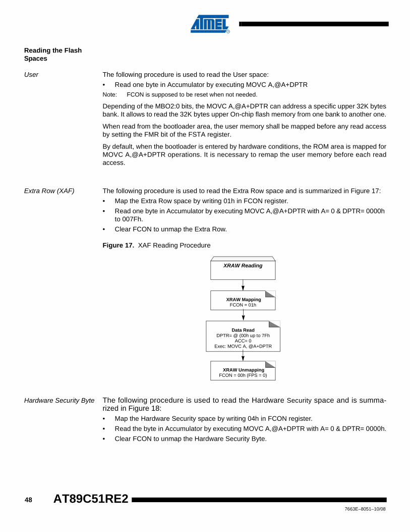
Extra Row (XAF) The following procedure is used to read the Extra Row space and is summarized in Figure 17:
• Map the Extra Row space by writing 01h in FCON register.
• Read one byte in Accumulator by executing MOVC A,@A+DPTR with A= 0 & DPTR= 0000h to 007Fh.
• Clear FCON to unmap the Extra Row.
Figure 17. XAF Reading Procedure
Hardware Security Byte The following procedure is used to read the Hardware Security space and is summa-rized in Figure 18:• Map the Hardware Security space by writing 04h in FCON register.
• Read the byte in Accumulator by executing MOVC A,@A+DPTR with A= 0 & DPTR= 0000h.
• Clear FCON to unmap the Hardware Security Byte.
XRAW Reading
Data ReadDPTR= @ (00h up to 7Fh
ACC= 0Exec: MOVC A, @A+DPTR
XRAW MappingFCON = 01h
XRAW UnmappingFCON = 00h (FPS = 0)
487663E–8051–10/08
AT89C51RE2
AT89C51RE2
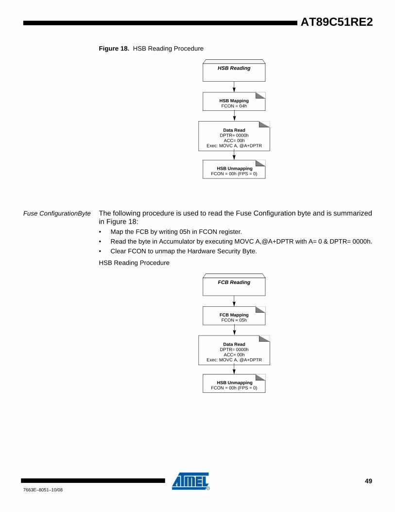
Figure 18. HSB Reading Procedure
Fuse ConfigurationByte The following procedure is used to read the Fuse Configuration byte and is summarizedin Figure 18:• Map the FCB by writing 05h in FCON register.
• Read the byte in Accumulator by executing MOVC A,@A+DPTR with A= 0 & DPTR= 0000h.
• Clear FCON to unmap the Hardware Security Byte.
HSB Reading Procedure
HSB Reading
Data ReadDPTR= 0000h
ACC= 00hExec: MOVC A, @A+DPTR
HSB MappingFCON = 04h
HSB UnmappingFCON = 00h (FPS = 0)
FCB Reading
Data ReadDPTR= 0000h
ACC= 00hExec: MOVC A, @A+DPTR
FCB MappingFCON = 05h
HSB UnmappingFCON = 00h (FPS = 0)
497663E–8051–10/08
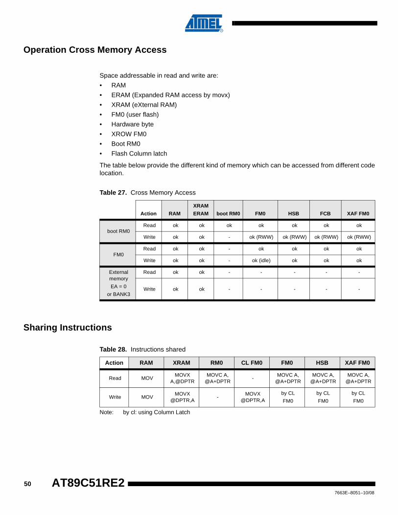
Operation Cross Memory Access
Space addressable in read and write are:
• RAM
• ERAM (Expanded RAM access by movx)
• XRAM (eXternal RAM)
• FM0 (user flash)
• Hardware byte
• XROW FM0
• Boot RM0
• Flash Column latch
The table below provide the different kind of memory which can be accessed from different codelocation.
Table 27. Cross Memory Access
Sharing Instructions
Table 28. Instructions shared
Note: by cl: using Column Latch
Action RAM
XRAM
ERAM boot RM0 FM0 HSB FCB XAF FM0
boot RM0Read ok ok ok ok ok ok ok
Write ok ok - ok (RWW) ok (RWW) ok (RWW) ok (RWW)
FM0Read ok ok - ok ok ok ok
Write ok ok - ok (idle) ok ok ok
External memory
EA = 0
or BANK3
Read ok ok - - - - -
Write ok ok - - - - -
Action RAM XRAM RM0 CL FM0 FM0 HSB XAF FM0
Read MOVMOVX
A,@DPTRMOVC A,
@A+DPTR-
MOVC A, @A+DPTR
MOVC A, @A+DPTR
MOVC A, @A+DPTR
Write MOVMOVX
@DPTR,A-
MOVX @DPTR,A
by CL
FM0
by CL
FM0
by CL
FM0
507663E–8051–10/08
AT89C51RE2

AT89C51RE2
Table 29. Write MOVX @DPTR,A
Table 30. MOVC A, @A+DPTR executed from External code EA=0
Table 31. MOVC A, @A+DPTR executed from External code EA=1, PC>=0x8000, FBS=Bank3
FPS of FCCON EA
XRAMERAM CL FM0
0 X winner
11 winner
0 winner
FMOD2:0FBS
(Fetch)MBO
(Target)MOVC A,@A+DPTR
X X X Read External Code
FMOD2:0MBO
(Target)DPTR MOVC A,@A+DPTR
X X < 0x8000Depends on FLB2:0
Can Returns Random value, for secured part.
X >= 0x8000 External code read
517663E–8051–10/08

Flash Protection from Parallel Programming The three lock bits in Hardware Security Byte (see "In-System Programming" section) are pro-grammed according to Table 32 provide different level of protection for the on-chip flash memoryFM0.
They are set by default to level 4
Table 32. Program Lock Bit FLB2-0
Program Lock bits
U: unprogrammed
P: programmed
WARNING: Security level 2 and 3 should only be programmed after verification.
Program Lock Bits
Protection DescriptionSecurity
levelFLB0 FLB1 FLB2
1 U U U No program lock features enabled.
2 P U U
MOVC instruction executed from external program memory are disabled from fetching code bytes from internal memory, EA is sampled and latched on reset, and further parallel programming of the Flash is disabled.
ISP allows only flash verification (no write operations are allowed) but IAP from internal code still allowed.
3 U P USame as 2, also verify through parallel programming interface is disabled and ISP read operation not allowed.
4 U U P Same as 3, also external execution is disabled (external bank not accessible)
527663E–8051–10/08
AT89C51RE2
AT89C51RE2
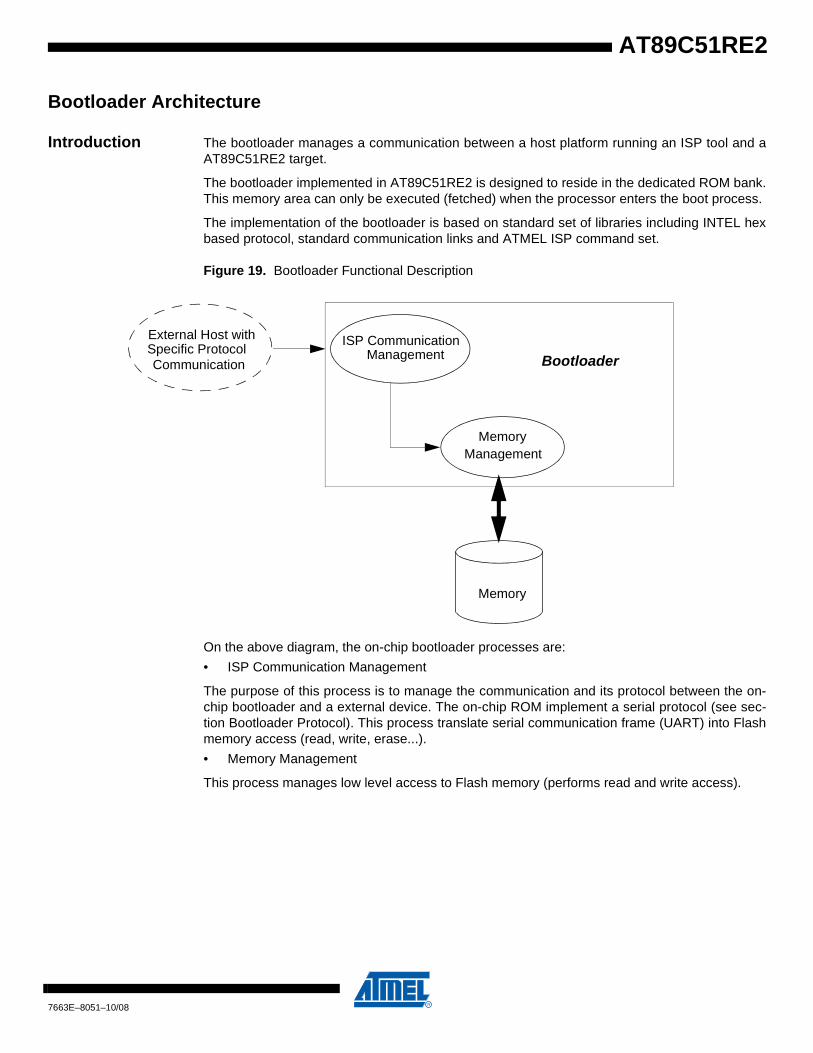
Bootloader Architecture
Introduction The bootloader manages a communication between a host platform running an ISP tool and aAT89C51RE2 target.
The bootloader implemented in AT89C51RE2 is designed to reside in the dedicated ROM bank.This memory area can only be executed (fetched) when the processor enters the boot process.
The implementation of the bootloader is based on standard set of libraries including INTEL hexbased protocol, standard communication links and ATMEL ISP command set.
Figure 19. Bootloader Functional Description
On the above diagram, the on-chip bootloader processes are:
• ISP Communication Management
The purpose of this process is to manage the communication and its protocol between the on-chip bootloader and a external device. The on-chip ROM implement a serial protocol (see sec-tion Bootloader Protocol). This process translate serial communication frame (UART) into Flashmemory access (read, write, erase...).
• Memory Management
This process manages low level access to Flash memory (performs read and write access).
ISP CommunicationManagementSpecific Protocol
Communication
Management
Memory
External Host with
Memory
Bootloader
537663E–8051–10/08
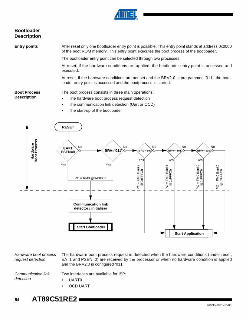
Bootloader Description
Entry points After reset only one bootloader entry point is possible. This entry point stands at address 0x0000of the boot ROM memory. This entry point executes the boot process of the bootloader.
The bootloader entry point can be selected through two processes:
At reset, if the hardware conditions are applied, the bootloader entry point is accessed andexecuted.
At reset, if the hardware conditions are not set and the BRV2-0 is programmed ‘011’, the boot-loader entry point is accessed and the bootprocess is started.
Boot Process Description
The boot process consists in three main operations:
• The hardware boot process request detection
• The communication link detection (Uart or OCD)
• The start-up of the bootloader
Hardware boot process request detection
The hardware boot process request is detected when the hardware conditions (under reset,EA=1 and PSEN=0) are received by the processor or when no hardware condition is appliedand the BRV2:0 is configured ‘011’.
Communication link detection
Two interfaces are available for ISP:
• UART0
• OCD UART
Har
dw
are
Bo
ot
Pro
cess
RESET
BRV=’011’
PC = RM0 @0x0000h
Communication link
Start Bootloader
Start Application
BRV=’100’EA=1
PSEN=0
Yes
No
Yes
No
detector / initialiser
Yes
NoBRV=’101’
Yes
NoBRV=’110’
Yes
No
PC
= F
M0
Ban
k2@
0xF
FF
Ch
PC
= F
M0
Ban
k1@
0xF
FF
Ch
PC
= F
M0
Ban
k0@
0xF
FF
Ch
PC
= F
M0
Ban
k0@
0xF
FF
Ch
547663E–8051–10/08
AT89C51RE2
AT89C51RE2
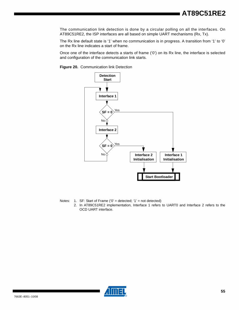
The communication link detection is done by a circular polling on all the interfaces. OnAT89C51RE2, the ISP interfaces are all based on simple UART mechanisms (Rx, Tx).
The Rx line default state is ‘1’ when no communication is in progress. A transition from ‘1’ to ‘0’on the Rx line indicates a start of frame.
Once one of the interface detects a starts of frame (‘0’) on its Rx line, the interface is selectedand configuration of the communication link starts.
Figure 20. Communication link Detection
Notes: 1. SF: Start of Frame (‘0’ = detected; ‘1’ = not detected)2. In AT89C51RE2 implementation, Interface 1 refers to UART0 and Interface 2 refers to the
OCD UART interface.
Yes
No
Interface 1
SF = 0
Yes
No
Interface 2
SF = 0
DetectionStart
Interface 1Initialisation
Interface 2Initialisation
Start Bootloader
557663E–8051–10/08
ISP Protocol Description
Physical Layer The UART used to transmit information has the following configuration:
• Character: 8-bit data
• Parity: none
• Stop: 1 bit
• Flow control: none
• Baud rate: autobaud is performed by the bootloader to compute the baud rate chosen by the host.
Frame Description The Serial Protocol is based on the Intel Extended Hex-type records.
Intel Hex records consist of ASCII characters used to represent hexadecimal values and aresummarized below.
Table 33. Intel Hex Type Frame
• Record Mark:
– Record Mark is the start of frame. This field must contain’:’.
• Record length:
– Record length specifies the number of Bytes of information or data which follows the Record Type field of the record.
• Load Offset:
– Load Offset specifies the 16-bit starting load offset of the data Bytes, therefore this field is used only for
– Data Program Record.
• Record Type:
– Record Type specifies the command type. This field is used to interpret the remaining information within the frame.
• Data/Info:
– Data/Info is a variable length field. It consists of zero or more Bytes encoded as pairs of hexadecimal digits. The meaning of data depends on the Record Type.
• Checksum:
– Checksum is the two’s complement of the 8-bit Bytes that result from converting each pair of ASCII hexadecimal digits to one Byte of binary, thus including all field from the Record Length field to the last Byte of the Data/Info field. Therefore, the sum of all the ASCII pairs in a record after converting to binary, including all field from the Record Length field to the Checksum field, is zero.
Record Mark ‘:’ Record length Load Offset Record Type Data or Info Checksum
1 byte 1 byte 2 bytes 1 bytes n byte 1 byte
567663E–8051–10/08
AT89C51RE2
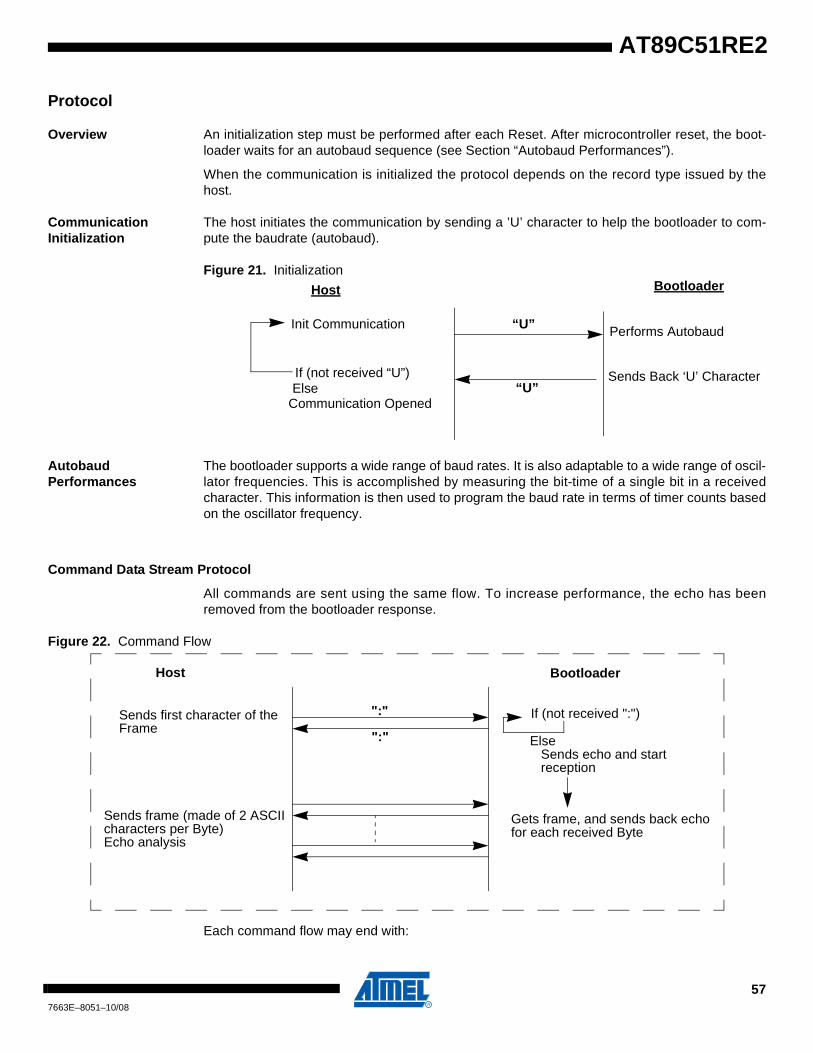
AT89C51RE2
Protocol
Overview An initialization step must be performed after each Reset. After microcontroller reset, the boot-loader waits for an autobaud sequence (see Section “Autobaud Performances”).
When the communication is initialized the protocol depends on the record type issued by thehost.
Communication Initialization
The host initiates the communication by sending a ’U’ character to help the bootloader to com-pute the baudrate (autobaud).
Figure 21. Initialization
Autobaud Performances
The bootloader supports a wide range of baud rates. It is also adaptable to a wide range of oscil-lator frequencies. This is accomplished by measuring the bit-time of a single bit in a receivedcharacter. This information is then used to program the baud rate in terms of timer counts basedon the oscillator frequency.
Command Data Stream Protocol
All commands are sent using the same flow. To increase performance, the echo has beenremoved from the bootloader response.
Figure 22. Command Flow
Each command flow may end with:
Host Bootloader
“U” Performs Autobaud Init Communication
If (not received “U”) “U”
Communication OpenedElse
Sends Back ‘U’ Character
Bootloader
":"Sends first character of theFrame
If (not received ":")
Sends frame (made of 2 ASCII Gets frame, and sends back echofor each received Byte
Host
Else":" Sends echo and start reception
characters per Byte)Echo analysis
577663E–8051–10/08

• “X”: If checksum error
• “L”: If read security is set
• “P”: If program security is set
• “.”: If command ok
• byte + “.”: read byte ok
587663E–8051–10/08
AT89C51RE2
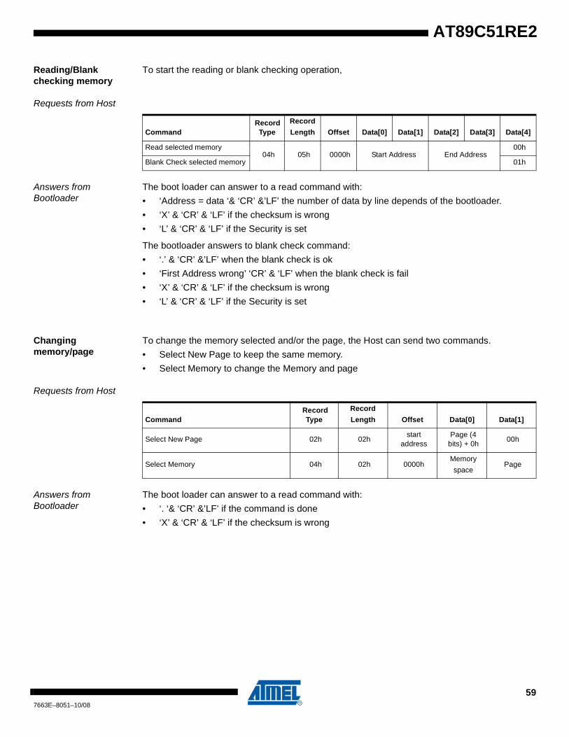
AT89C51RE2
Reading/Blank checking memory
To start the reading or blank checking operation,
Requests from Host
Answers from Bootloader
The boot loader can answer to a read command with:
• ‘Address = data ‘& ‘CR’ &’LF’ the number of data by line depends of the bootloader.
• ‘X’ & ‘CR’ & ‘LF’ if the checksum is wrong
• ‘L’ & ‘CR’ & ‘LF’ if the Security is set
The bootloader answers to blank check command:
• ‘.’ & ‘CR’ &’LF’ when the blank check is ok
• ‘First Address wrong’ ‘CR’ & ‘LF’ when the blank check is fail
• ‘X’ & ‘CR’ & ‘LF’ if the checksum is wrong
• ‘L’ & ‘CR’ & ‘LF’ if the Security is set
Changing memory/page
To change the memory selected and/or the page, the Host can send two commands.
• Select New Page to keep the same memory.
• Select Memory to change the Memory and page
Requests from Host
Answers from Bootloader
The boot loader can answer to a read command with:
• ‘. ‘& ‘CR’ &’LF’ if the command is done
• ‘X’ & ‘CR’ & ‘LF’ if the checksum is wrong
Command Record
Type
Record
Length Offset Data[0] Data[1] Data[2] Data[3] Data[4]
Read selected memory04h 05h 0000h Start Address End Address
00h
Blank Check selected memory 01h
Command Record
Type
Record
Length Offset Data[0] Data[1]
Select New Page 02h 02hstart
addressPage (4
bits) + 0h00h
Select Memory 04h 02h 0000hMemory
spacePage
597663E–8051–10/08
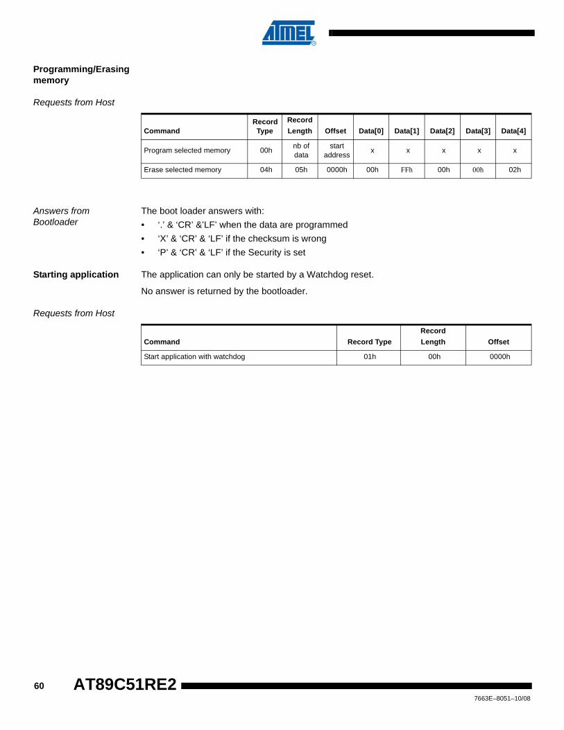
Programming/Erasing memory
Requests from Host
Answers from Bootloader
The boot loader answers with:
• ‘.’ & ‘CR’ &’LF’ when the data are programmed
• ‘X’ & ‘CR’ & ‘LF’ if the checksum is wrong
• ‘P’ & ‘CR’ & ‘LF’ if the Security is set
Starting application The application can only be started by a Watchdog reset.
No answer is returned by the bootloader.
Requests from Host
Command Record
Type
Record
Length Offset Data[0] Data[1] Data[2] Data[3] Data[4]
Program selected memory 00hnb of data
start address
x x x x x
Erase selected memory 04h 05h 0000h 00h FFh 00h 00h 02h
Command Record Type
Record
Length Offset
Start application with watchdog 01h 00h 0000h
607663E–8051–10/08
AT89C51RE2
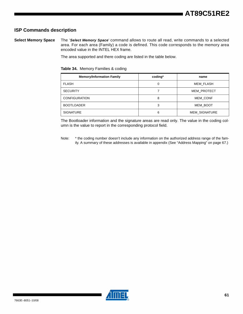
AT89C51RE2
ISP Commands description
Select Memory Space The ‘Select Memory Space’ command allows to route all read, write commands to a selectedarea. For each area (Family) a code is defined. This code corresponds to the memory areaencoded value in the INTEL HEX frame.
The area supported and there coding are listed in the table below.
Table 34. Memory Families & coding
The Bootloader information and the signature areas are read only. The value in the coding col-umn is the value to report in the corresponding protocol field.
Note: * the coding number doesn’t include any information on the authorized address range of the fam-ily. A summary of these addresses is available in appendix (See “Address Mapping” on page 67.)
Memory/Information Family coding* name
FLASH 0 MEM_FLASH
SECURITY 7 MEM_PROTECT
CONFIGURATION 8 MEM_CONF
BOOTLOADER 3 MEM_BOOT
SIGNATURE 6 MEM_SIGNATURE
617663E–8051–10/08
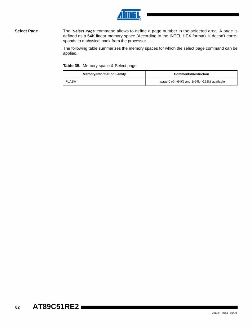
Select Page The ‘Select Page’ command allows to define a page number in the selected area. A page isdefined as a 64K linear memory space (According to the INTEL HEX format). It doesn’t corre-sponds to a physical bank from the processor.
The following table summarizes the memory spaces for which the select page command can beapplied.
Table 35. Memory space & Select page
Memory/Information Family Comments/Restriction
FLASH page 0 (0->64K) and 1(64k->128k) available
627663E–8051–10/08
AT89C51RE2
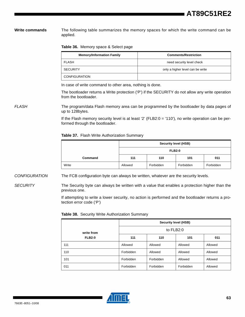
AT89C51RE2
Write commands The following table summarizes the memory spaces for which the write command can beapplied.
Table 36. Memory space & Select page
In case of write command to other area, nothing is done.
The bootloader returns a Write protection (‘P’) if the SECURITY do not allow any write operationfrom the bootloader.
FLASH The program/data Flash memory area can be programmed by the bootloader by data pages ofup to 128bytes.
If the Flash memory security level is at least ‘2’ (FLB2:0 = ‘110’), no write operation can be per-formed through the bootloader.
Table 37. Flash Write Authorization Summary
CONFIGURATION The FCB configuration byte can always be written, whatever are the security levels.
SECURITY The Security byte can always be written with a value that enables a protection higher than theprevious one.
If attempting to write a lower security, no action is performed and the bootloader returns a pro-tection error code (‘P’)
Table 38. Security Write Authorization Summary
Memory/Information Family Comments/Restriction
FLASH need security level check
SECURITY only a higher level can be write
CONFIGURATION
Command
Security level (HSB)
FLB2:0
111 110 101 011
Write Allowed Forbidden Forbidden Forbidden
write from
FLB2:0
Security level (HSB)
to FLB2:0
111 110 101 011
111 Allowed Allowed Allowed Allowed
110 Forbidden Allowed Allowed Allowed
101 Forbidden Forbidden Allowed Allowed
011 Forbidden Forbidden Forbidden Allowed
637663E–8051–10/08
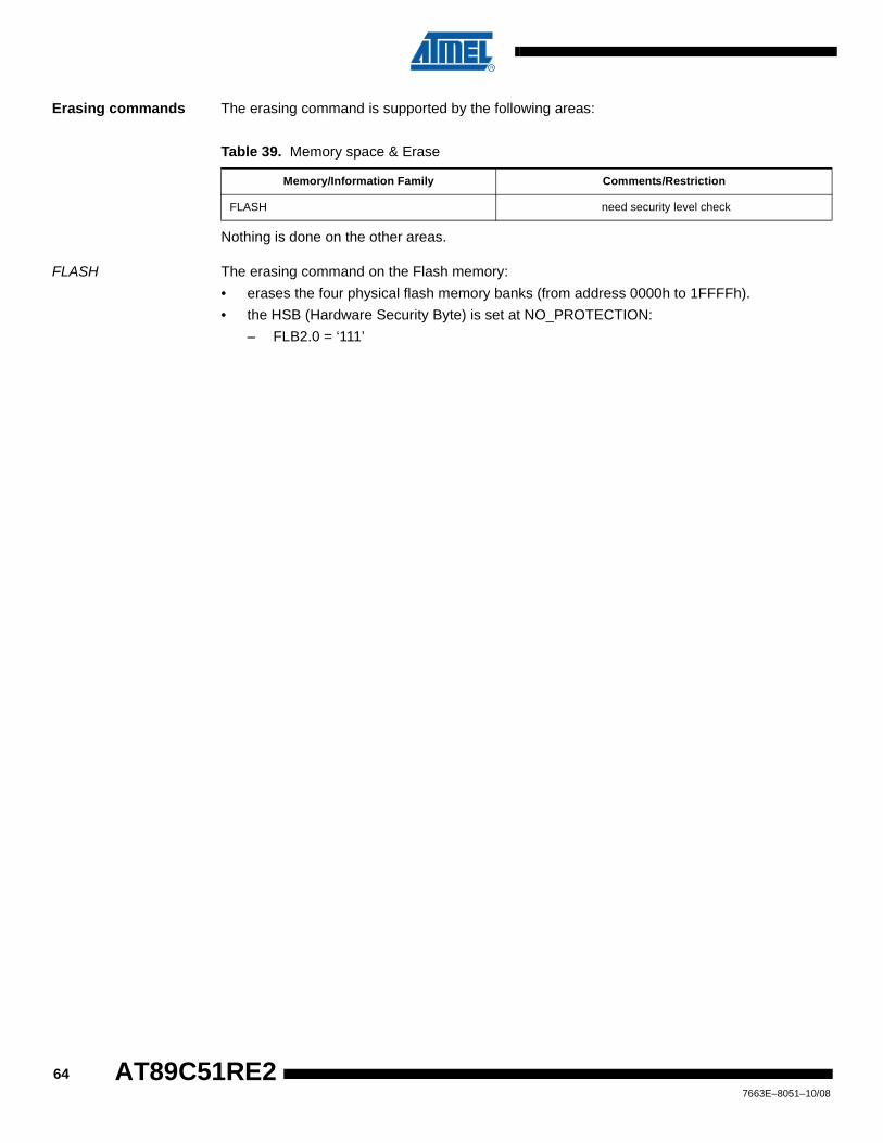
Erasing commands The erasing command is supported by the following areas:
Table 39. Memory space & Erase
Nothing is done on the other areas.
FLASH The erasing command on the Flash memory:
• erases the four physical flash memory banks (from address 0000h to 1FFFFh).
• the HSB (Hardware Security Byte) is set at NO_PROTECTION:
– FLB2.0 = ‘111’
Memory/Information Family Comments/Restriction
FLASH need security level check
647663E–8051–10/08
AT89C51RE2
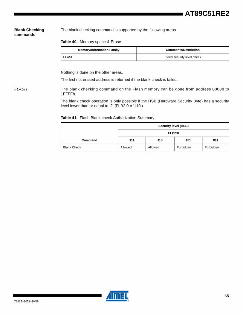
AT89C51RE2
Blank Checking commands
The blank checking command is supported by the following areas
Table 40. Memory space & Erase
Nothing is done on the other areas.
The first not erased address is returned if the blank check is failed.
FLASH The blank checking command on the Flash memory can be done from address 0000h to1FFFFh.
The blank check operation is only possible if the HSB (Hardware Security Byte) has a securitylevel lower than or equal to ‘2’ (FLB2.0 = ‘110’)
Table 41. Flash Blank check Authorization Summary
Memory/Information Family Comments/Restriction
FLASH need security level check
Command
Security level (HSB)
FLB2:0
111 110 101 011
Blank Check Allowed Allowed Forbidden Forbidden
657663E–8051–10/08
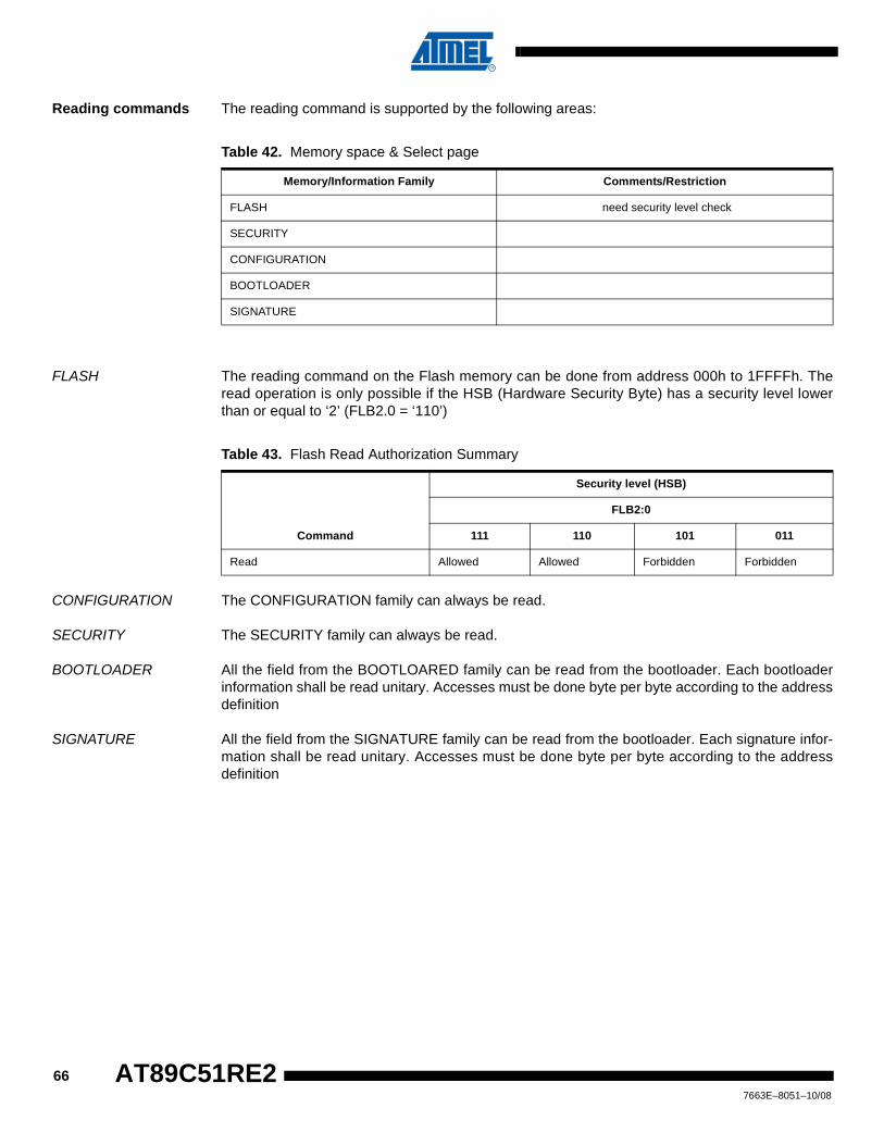
Reading commands The reading command is supported by the following areas:
Table 42. Memory space & Select page
FLASH The reading command on the Flash memory can be done from address 000h to 1FFFFh. Theread operation is only possible if the HSB (Hardware Security Byte) has a security level lowerthan or equal to ‘2’ (FLB2.0 = ‘110’)
Table 43. Flash Read Authorization Summary
CONFIGURATION The CONFIGURATION family can always be read.
SECURITY The SECURITY family can always be read.
BOOTLOADER All the field from the BOOTLOARED family can be read from the bootloader. Each bootloaderinformation shall be read unitary. Accesses must be done byte per byte according to the addressdefinition
SIGNATURE All the field from the SIGNATURE family can be read from the bootloader. Each signature infor-mation shall be read unitary. Accesses must be done byte per byte according to the addressdefinition
Memory/Information Family Comments/Restriction
FLASH need security level check
SECURITY
CONFIGURATION
BOOTLOADER
SIGNATURE
Command
Security level (HSB)
FLB2:0
111 110 101 011
Read Allowed Allowed Forbidden Forbidden
667663E–8051–10/08
AT89C51RE2

AT89C51RE2
Start Application The start application command is used to quit the bootloader and start the application loaded.
The start application is performed by a watchdog reset.
The best way to start the application from a user defined entry point is to configure the FCB(Fuse Configuration Byte) before launching the watchdog. Then, depending on the configurationof the BRV2:0 field, the hardware boots from the selected memory area.
ISP Command summary
UART Protocol frames
Address MappingTable 45. Memory Families, Addresses & Coding
Attempting an access with any other ‘coding’, ‘page number’ or ‘Address’ results in no actionand no answer from the bootloader.
Table 44. Summary of frames from Host
Command Record
Type
Record
Length Offset Data[0] Data[1] Data[2] Data[3] Data[4]
Program selected memory 00h nb of datastart
addressx x x x x
Start application with watchdog 01h 00h 0000h x x x x x
Select New Page 02h 02hstart
addressPage (4
bits) + 0h00h x x x
Select Memory
04h
02h 0000hMemory
spacePage x x x
Read selected memory
05h 0000hStart Address End Address
00h
Blank Check selected memory 01h
Erase Selected memory 00h FFh 00h 00h 02h
Memory/Parameter coding Address Page numberMemory/Information
Family
FLASH 0 0 up to 0x1FFFF 0 up to 1 FLASH
HSB 7 0 0 SECURITY
FCB 8 0 0 CONFIGURATION
Bootloader revision
3
00h
0 BOOTLOADERBoot id1 01h
Boot id2 02h
Manuf. code
6
30h
0 SIGNATUREFamily code 31h
Product name 60h
Product rev 61h
677663E–8051–10/08
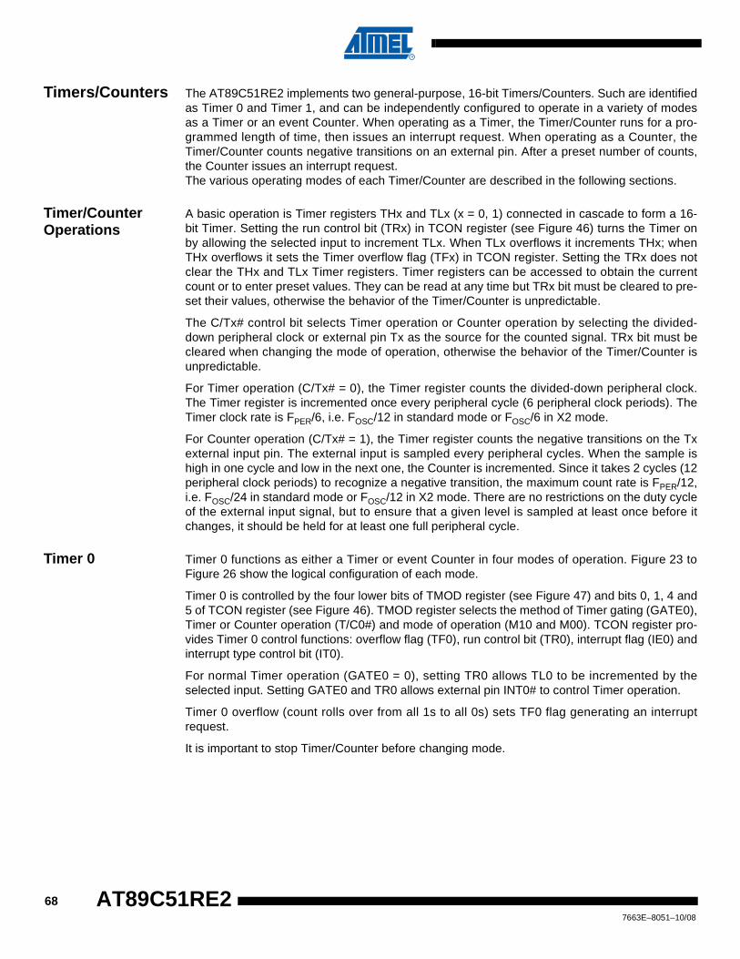
Timers/Counters The AT89C51RE2 implements two general-purpose, 16-bit Timers/Counters. Such are identifiedas Timer 0 and Timer 1, and can be independently configured to operate in a variety of modesas a Timer or an event Counter. When operating as a Timer, the Timer/Counter runs for a pro-grammed length of time, then issues an interrupt request. When operating as a Counter, theTimer/Counter counts negative transitions on an external pin. After a preset number of counts,the Counter issues an interrupt request.The various operating modes of each Timer/Counter are described in the following sections.
Timer/Counter Operations
A basic operation is Timer registers THx and TLx (x = 0, 1) connected in cascade to form a 16-bit Timer. Setting the run control bit (TRx) in TCON register (see Figure 46) turns the Timer onby allowing the selected input to increment TLx. When TLx overflows it increments THx; whenTHx overflows it sets the Timer overflow flag (TFx) in TCON register. Setting the TRx does notclear the THx and TLx Timer registers. Timer registers can be accessed to obtain the currentcount or to enter preset values. They can be read at any time but TRx bit must be cleared to pre-set their values, otherwise the behavior of the Timer/Counter is unpredictable.
The C/Tx# control bit selects Timer operation or Counter operation by selecting the divided-down peripheral clock or external pin Tx as the source for the counted signal. TRx bit must becleared when changing the mode of operation, otherwise the behavior of the Timer/Counter isunpredictable.
For Timer operation (C/Tx# = 0), the Timer register counts the divided-down peripheral clock.The Timer register is incremented once every peripheral cycle (6 peripheral clock periods). TheTimer clock rate is FPER/6, i.e. FOSC/12 in standard mode or FOSC/6 in X2 mode.
For Counter operation (C/Tx# = 1), the Timer register counts the negative transitions on the Txexternal input pin. The external input is sampled every peripheral cycles. When the sample ishigh in one cycle and low in the next one, the Counter is incremented. Since it takes 2 cycles (12peripheral clock periods) to recognize a negative transition, the maximum count rate is FPER/12,i.e. FOSC/24 in standard mode or FOSC/12 in X2 mode. There are no restrictions on the duty cycleof the external input signal, but to ensure that a given level is sampled at least once before itchanges, it should be held for at least one full peripheral cycle.
Timer 0 Timer 0 functions as either a Timer or event Counter in four modes of operation. Figure 23 toFigure 26 show the logical configuration of each mode.
Timer 0 is controlled by the four lower bits of TMOD register (see Figure 47) and bits 0, 1, 4 and5 of TCON register (see Figure 46). TMOD register selects the method of Timer gating (GATE0),Timer or Counter operation (T/C0#) and mode of operation (M10 and M00). TCON register pro-vides Timer 0 control functions: overflow flag (TF0), run control bit (TR0), interrupt flag (IE0) andinterrupt type control bit (IT0).
For normal Timer operation (GATE0 = 0), setting TR0 allows TL0 to be incremented by theselected input. Setting GATE0 and TR0 allows external pin INT0# to control Timer operation.
Timer 0 overflow (count rolls over from all 1s to all 0s) sets TF0 flag generating an interruptrequest.
It is important to stop Timer/Counter before changing mode.
687663E–8051–10/08
AT89C51RE2
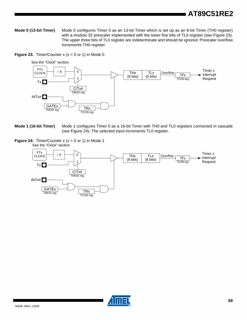
AT89C51RE2
Mode 0 (13-bit Timer) Mode 0 configures Timer 0 as an 13-bit Timer which is set up as an 8-bit Timer (TH0 register)with a modulo 32 prescaler implemented with the lower five bits of TL0 register (see Figure 23).The upper three bits of TL0 register are indeterminate and should be ignored. Prescaler overflowincrements TH0 register.
Figure 23. Timer/Counter x (x = 0 or 1) in Mode 0
Mode 1 (16-bit Timer) Mode 1 configures Timer 0 as a 16-bit Timer with TH0 and TL0 registers connected in cascade(see Figure 24). The selected input increments TL0 register.
Figure 24. Timer/Counter x (x = 0 or 1) in Mode 1
FTxCLOCK
TRxTCON reg
TFxTCON reg
0
1
GATExTMOD reg
÷ 6 OverflowTimer xInterruptRequest
C/Tx#TMOD reg
TLx(5 bits)
THx(8 bits)
INTx#
Tx
See the “Clock” section
TRxTCON reg
TFxTCON reg
0
1
GATExTMOD reg
OverflowTimer xInterruptRequest
C/Tx#TMOD reg
TLx(8 bits)
THx(8 bits)
INTx#
Tx
FTxCLOCK ÷ 6
See the “Clock” section
697663E–8051–10/08
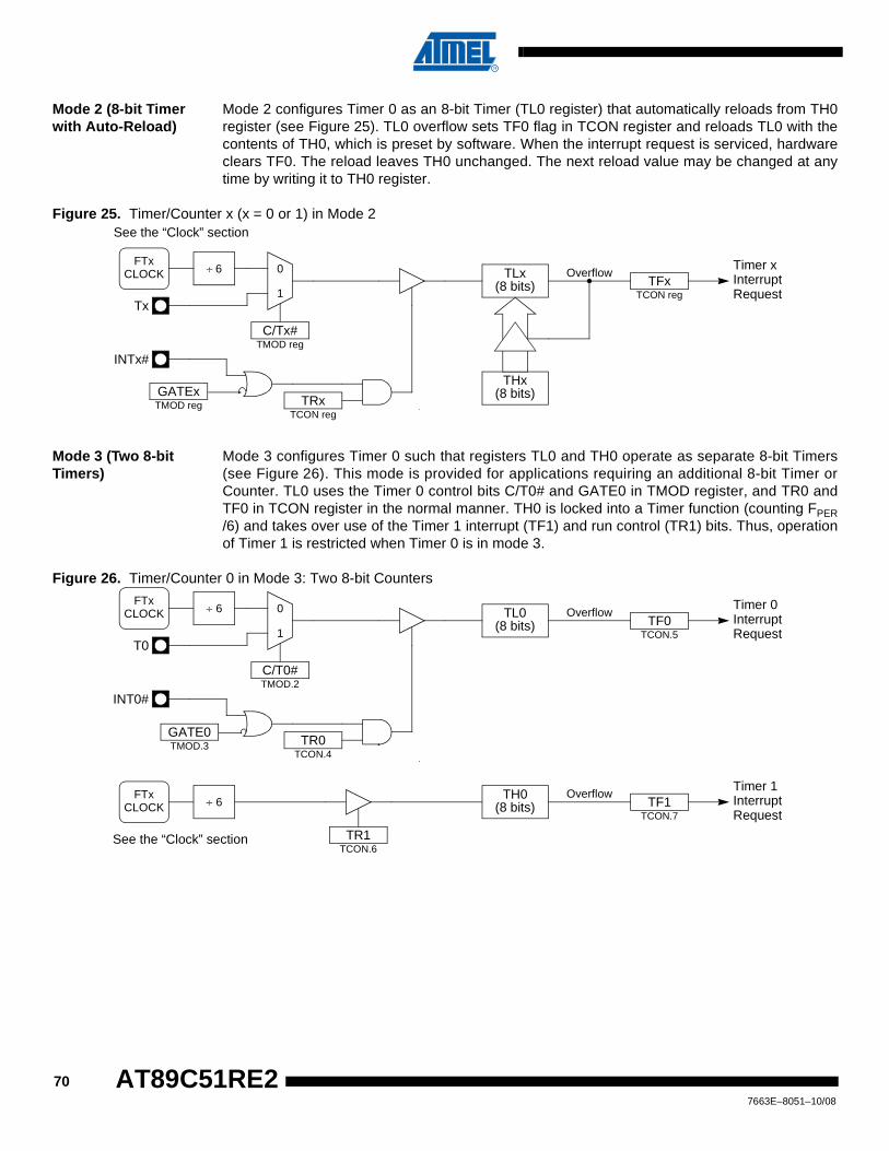
Mode 2 (8-bit Timer with Auto-Reload)
Mode 2 configures Timer 0 as an 8-bit Timer (TL0 register) that automatically reloads from TH0register (see Figure 25). TL0 overflow sets TF0 flag in TCON register and reloads TL0 with thecontents of TH0, which is preset by software. When the interrupt request is serviced, hardwareclears TF0. The reload leaves TH0 unchanged. The next reload value may be changed at anytime by writing it to TH0 register.
Figure 25. Timer/Counter x (x = 0 or 1) in Mode 2
Mode 3 (Two 8-bit Timers)
Mode 3 configures Timer 0 such that registers TL0 and TH0 operate as separate 8-bit Timers(see Figure 26). This mode is provided for applications requiring an additional 8-bit Timer orCounter. TL0 uses the Timer 0 control bits C/T0# and GATE0 in TMOD register, and TR0 andTF0 in TCON register in the normal manner. TH0 is locked into a Timer function (counting FPER/6) and takes over use of the Timer 1 interrupt (TF1) and run control (TR1) bits. Thus, operationof Timer 1 is restricted when Timer 0 is in mode 3.
Figure 26. Timer/Counter 0 in Mode 3: Two 8-bit Counters
TRxTCON reg
TFxTCON reg
0
1
GATExTMOD reg
OverflowTimer xInterruptRequest
C/Tx#TMOD reg
TLx(8 bits)
THx(8 bits)
INTx#
Tx
FTxCLOCK ÷ 6
See the “Clock” section
TR0TCON.4
TF0TCON.5
INT0#
0
1
GATE0TMOD.3
OverflowTimer 0InterruptRequest
C/T0#TMOD.2
TL0(8 bits)
TR1TCON.6
TH0(8 bits) TF1
TCON.7
OverflowTimer 1InterruptRequest
T0
FTxCLOCK ÷ 6
FTxCLOCK ÷ 6
See the “Clock” section
707663E–8051–10/08
AT89C51RE2
AT89C51RE2
Timer 1 Timer 1 is identical to Timer 0 excepted for Mode 3 which is a hold-count mode. The followingcomments help to understand the differences:
• Timer 1 functions as either a Timer or event Counter in three modes of operation. Figure 23 to Figure 25 show the logical configuration for modes 0, 1, and 2. Timer 1’s mode 3 is a hold-count mode.
• Timer 1 is controlled by the four high-order bits of TMOD register (see Figure 47) and bits 2, 3, 6 and 7 of TCON register (see Figure 46). TMOD register selects the method of Timer gating (GATE1), Timer or Counter operation (C/T1#) and mode of operation (M11 and M01). TCON register provides Timer 1 control functions: overflow flag (TF1), run control bit (TR1), interrupt flag (IE1) and interrupt type control bit (IT1).
• Timer 1 can serve as the Baud Rate Generator for the Serial Port. Mode 2 is best suited for this purpose.
• For normal Timer operation (GATE1 = 0), setting TR1 allows TL1 to be incremented by the selected input. Setting GATE1 and TR1 allows external pin INT1# to control Timer operation.
• Timer 1 overflow (count rolls over from all 1s to all 0s) sets the TF1 flag generating an interrupt request.
• When Timer 0 is in mode 3, it uses Timer 1’s overflow flag (TF1) and run control bit (TR1). For this situation, use Timer 1 only for applications that do not require an interrupt (such as a Baud Rate Generator for the Serial Port) and switch Timer 1 in and out of mode 3 to turn it off and on.
• It is important to stop Timer/Counter before changing mode.
Mode 0 (13-bit Timer) Mode 0 configures Timer 1 as a 13-bit Timer, which is set up as an 8-bit Timer (TH1 register)with a modulo-32 prescaler implemented with the lower 5 bits of the TL1 register (seeFigure 23). The upper 3 bits of TL1 register are ignored. Prescaler overflow increments TH1register.
Mode 1 (16-bit Timer) Mode 1 configures Timer 1 as a 16-bit Timer with TH1 and TL1 registers connected in cascade(see Figure 24). The selected input increments TL1 register.
Mode 2 (8-bit Timer with Auto-Reload)
Mode 2 configures Timer 1 as an 8-bit Timer (TL1 register) with automatic reload from TH1 reg-ister on overflow (see Figure 25). TL1 overflow sets TF1 flag in TCON register and reloads TL1with the contents of TH1, which is preset by software. The reload leaves TH1 unchanged.
Mode 3 (Halt) Placing Timer 1 in mode 3 causes it to halt and hold its count. This can be used to halt Timer 1when TR1 run control bit is not available i.e. when Timer 0 is in mode 3.
Interrupt Each Timer handles one interrupt source that is the timer overflow flag TF0 or TF1. This flag isset every time an overflow occurs. Flags are cleared when vectoring to the Timer interrupt rou-tine. Interrupts are enabled by setting ETx bit in IEN0 register. This assumes interrupts areglobally enabled by setting EA bit in IEN0 register.
717663E–8051–10/08

Figure 27. Timer Interrupt System
TF0TCON.5
ET0IEN0.1
Timer 0Interrupt Request
TF1TCON.7
ET1IEN0.3
Timer 1Interrupt Request
727663E–8051–10/08
AT89C51RE2
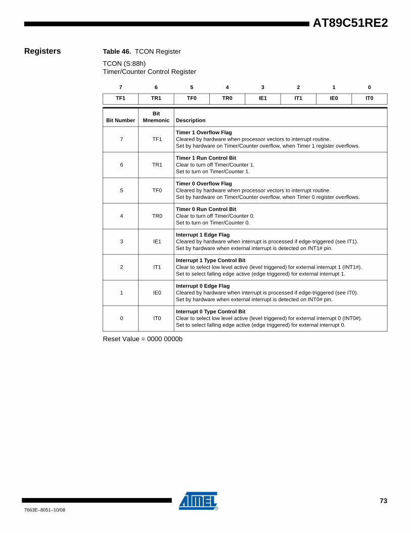
AT89C51RE2
Registers Table 46. TCON Register
TCON (S:88h)Timer/Counter Control Register
Reset Value = 0000 0000b
7 6 5 4 3 2 1 0
TF1 TR1 TF0 TR0 IE1 IT1 IE0 IT0
Bit NumberBit
Mnemonic Description
7 TF1Timer 1 Overflow FlagCleared by hardware when processor vectors to interrupt routine.Set by hardware on Timer/Counter overflow, when Timer 1 register overflows.
6 TR1Timer 1 Run Control BitClear to turn off Timer/Counter 1.Set to turn on Timer/Counter 1.
5 TF0Timer 0 Overflow FlagCleared by hardware when processor vectors to interrupt routine.Set by hardware on Timer/Counter overflow, when Timer 0 register overflows.
4 TR0Timer 0 Run Control BitClear to turn off Timer/Counter 0.Set to turn on Timer/Counter 0.
3 IE1Interrupt 1 Edge FlagCleared by hardware when interrupt is processed if edge-triggered (see IT1).Set by hardware when external interrupt is detected on INT1# pin.
2 IT1Interrupt 1 Type Control BitClear to select low level active (level triggered) for external interrupt 1 (INT1#).Set to select falling edge active (edge triggered) for external interrupt 1.
1 IE0Interrupt 0 Edge FlagCleared by hardware when interrupt is processed if edge-triggered (see IT0).Set by hardware when external interrupt is detected on INT0# pin.
0 IT0Interrupt 0 Type Control BitClear to select low level active (level triggered) for external interrupt 0 (INT0#).Set to select falling edge active (edge triggered) for external interrupt 0.
737663E–8051–10/08
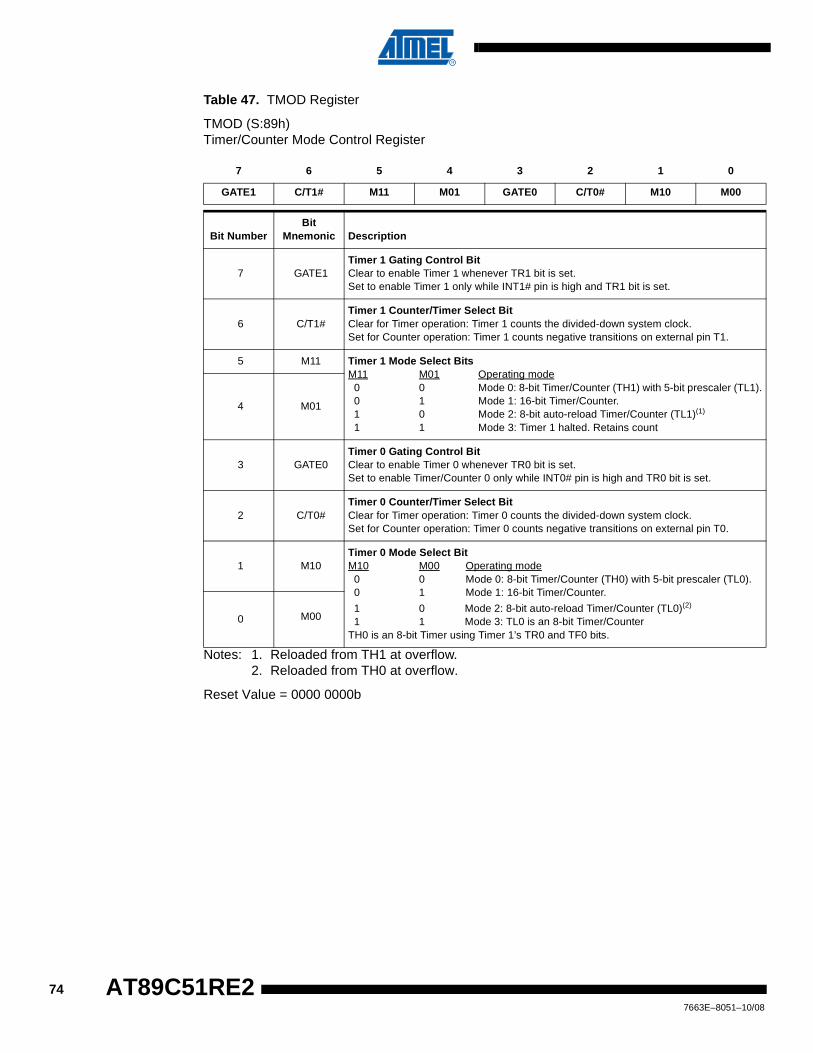
Table 47. TMOD Register
TMOD (S:89h)Timer/Counter Mode Control Register
Notes: 1. Reloaded from TH1 at overflow.2. Reloaded from TH0 at overflow.
Reset Value = 0000 0000b
7 6 5 4 3 2 1 0
GATE1 C/T1# M11 M01 GATE0 C/T0# M10 M00
Bit NumberBit
Mnemonic Description
7 GATE1Timer 1 Gating Control BitClear to enable Timer 1 whenever TR1 bit is set.Set to enable Timer 1 only while INT1# pin is high and TR1 bit is set.
6 C/T1#Timer 1 Counter/Timer Select BitClear for Timer operation: Timer 1 counts the divided-down system clock.Set for Counter operation: Timer 1 counts negative transitions on external pin T1.
5 M11 Timer 1 Mode Select BitsM11 M01 Operating mode 0 0 Mode 0: 8-bit Timer/Counter (TH1) with 5-bit prescaler (TL1). 0 1 Mode 1: 16-bit Timer/Counter.1 0 Mode 2: 8-bit auto-reload Timer/Counter (TL1)(1)
1 1 Mode 3: Timer 1 halted. Retains count
4 M01
3 GATE0Timer 0 Gating Control BitClear to enable Timer 0 whenever TR0 bit is set.Set to enable Timer/Counter 0 only while INT0# pin is high and TR0 bit is set.
2 C/T0#Timer 0 Counter/Timer Select BitClear for Timer operation: Timer 0 counts the divided-down system clock.Set for Counter operation: Timer 0 counts negative transitions on external pin T0.
1 M10Timer 0 Mode Select BitM10 M00 Operating mode 0 0 Mode 0: 8-bit Timer/Counter (TH0) with 5-bit prescaler (TL0). 0 1 Mode 1: 16-bit Timer/Counter.
1 0 Mode 2: 8-bit auto-reload Timer/Counter (TL0)(2)
1 1 Mode 3: TL0 is an 8-bit Timer/CounterTH0 is an 8-bit Timer using Timer 1’s TR0 and TF0 bits.
0 M00
747663E–8051–10/08
AT89C51RE2
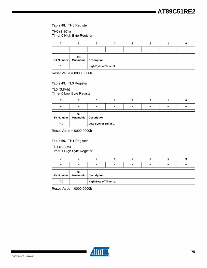
AT89C51RE2
Table 48. TH0 Register
TH0 (S:8Ch)Timer 0 High Byte Register
Reset Value = 0000 0000b
Table 49. TL0 Register
TL0 (S:8Ah)Timer 0 Low Byte Register
Reset Value = 0000 0000b
Table 50. TH1 Register
TH1 (S:8Dh)Timer 1 High Byte Register
Reset Value = 0000 0000b
7 6 5 4 3 2 1 0
– – – – – – – –
Bit NumberBit
Mnemonic Description
7:0 High Byte of Timer 0.
7 6 5 4 3 2 1 0
– – – – – – – –
Bit NumberBit
Mnemonic Description
7:0 Low Byte of Timer 0.
7 6 5 4 3 2 1 0
– – – – – – – –
Bit NumberBit
Mnemonic Description
7:0 High Byte of Timer 1.
757663E–8051–10/08
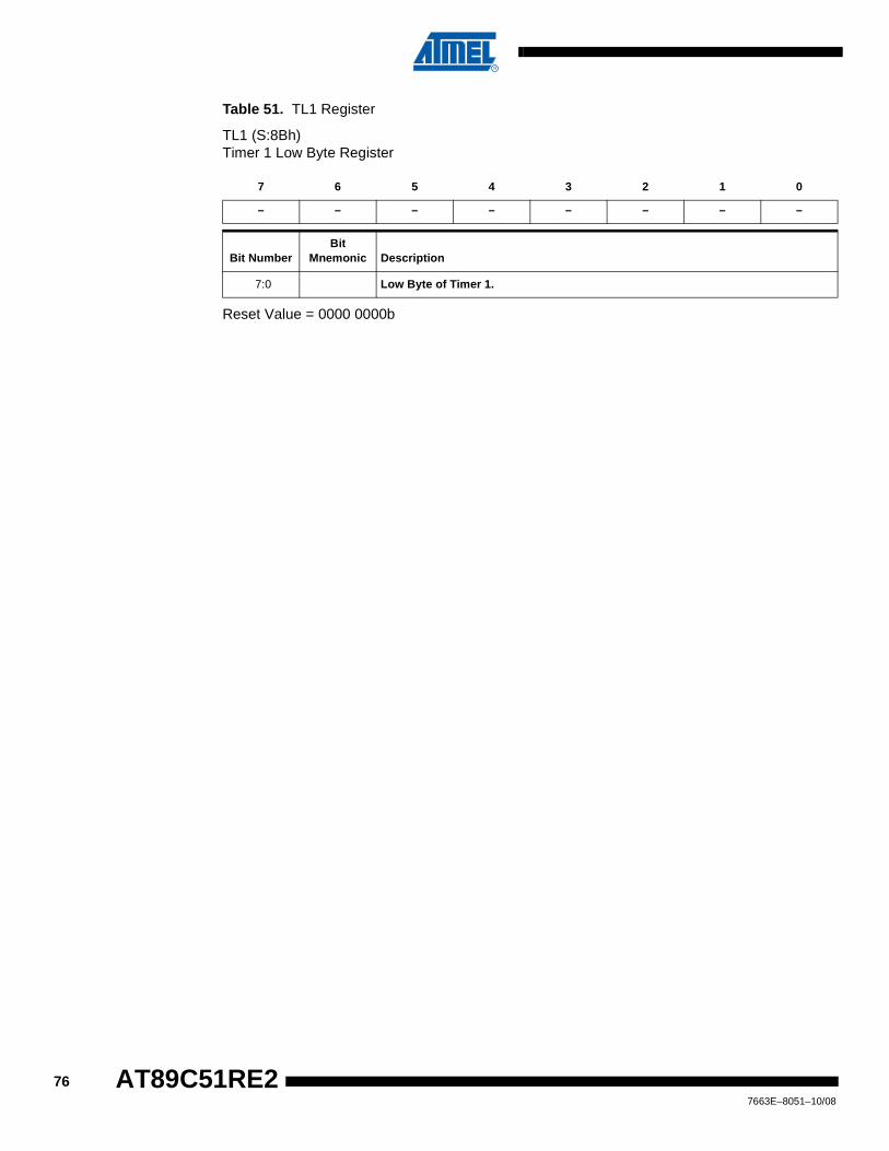
Table 51. TL1 Register
TL1 (S:8Bh)Timer 1 Low Byte Register
Reset Value = 0000 0000b
7 6 5 4 3 2 1 0
– – – – – – – –
Bit NumberBit
Mnemonic Description
7:0 Low Byte of Timer 1.
767663E–8051–10/08
AT89C51RE2
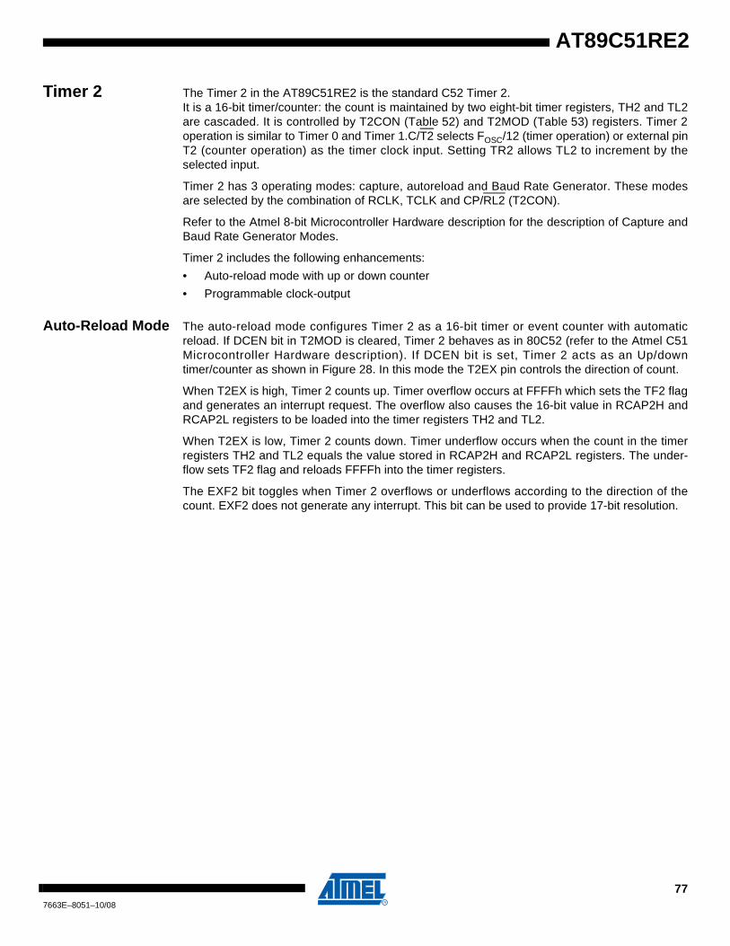
AT89C51RE2
Timer 2 The Timer 2 in the AT89C51RE2 is the standard C52 Timer 2.It is a 16-bit timer/counter: the count is maintained by two eight-bit timer registers, TH2 and TL2are cascaded. It is controlled by T2CON (Table 52) and T2MOD (Table 53) registers. Timer 2operation is similar to Timer 0 and Timer 1.C/T2 selects FOSC/12 (timer operation) or external pinT2 (counter operation) as the timer clock input. Setting TR2 allows TL2 to increment by theselected input.
Timer 2 has 3 operating modes: capture, autoreload and Baud Rate Generator. These modesare selected by the combination of RCLK, TCLK and CP/RL2 (T2CON).
Refer to the Atmel 8-bit Microcontroller Hardware description for the description of Capture andBaud Rate Generator Modes.
Timer 2 includes the following enhancements:
• Auto-reload mode with up or down counter
• Programmable clock-output
Auto-Reload Mode The auto-reload mode configures Timer 2 as a 16-bit timer or event counter with automaticreload. If DCEN bit in T2MOD is cleared, Timer 2 behaves as in 80C52 (refer to the Atmel C51Microcontroller Hardware description). If DCEN bit is set, Timer 2 acts as an Up/downtimer/counter as shown in Figure 28. In this mode the T2EX pin controls the direction of count.
When T2EX is high, Timer 2 counts up. Timer overflow occurs at FFFFh which sets the TF2 flagand generates an interrupt request. The overflow also causes the 16-bit value in RCAP2H andRCAP2L registers to be loaded into the timer registers TH2 and TL2.
When T2EX is low, Timer 2 counts down. Timer underflow occurs when the count in the timerregisters TH2 and TL2 equals the value stored in RCAP2H and RCAP2L registers. The under-flow sets TF2 flag and reloads FFFFh into the timer registers.
The EXF2 bit toggles when Timer 2 overflows or underflows according to the direction of thecount. EXF2 does not generate any interrupt. This bit can be used to provide 17-bit resolution.
777663E–8051–10/08
Figure 28. Auto-Reload Mode Up/Down Counter (DCEN = 1)
Programmable Clock-Output
In the clock-out mode, Timer 2 operates as a 50%-duty-cycle, programmable clock generator(See Figure 29). The input clock increments TL2 at frequency FCLK PERIPH/2.The timer repeatedlycounts to overflow from a loaded value. At overflow, the contents of RCAP2H and RCAP2L reg-isters are loaded into TH2 and TL2.In this mode, Timer 2 overflows do not generate interrupts.The formula gives the clock-out frequency as a function of the system oscillator frequency andthe value in the RCAP2H and RCAP2L registers:
For a 16 MHz system clock, Timer 2 has a programmable frequency range of 61 Hz (FCLK PERIPH/216) to 4 MHz (FCLK PERIPH/4). The generated clock signal is brought out to T2 pin(P1.0).
Timer 2 is programmed for the clock-out mode as follows:
• Set T2OE bit in T2MOD register.
• Clear C/T2 bit in T2CON register.
• Determine the 16-bit reload value from the formula and enter it in RCAP2H/RCAP2L registers.
• Enter a 16-bit initial value in timer registers TH2/TL2.It can be the same as the reload value or a different one depending on the application.
• To start the timer, set TR2 run control bit in T2CON register.
It is possible to use Timer 2 as a baud rate generator and a clock generator simultaneously. Forthis configuration, the baud rates and clock frequencies are not independent since both func-tions use the values in the RCAP2H and RCAP2L registers.
(DOWN COUNTING RELOAD VALUE)
C/T2
TF2
TR2
T2
EXF2
TH2(8-bit)
TL2(8-bit)
RCAP2H(8-bit)
RCAP2L(8-bit)
FFh(8-bit)
FFh(8-bit)
TOGGLE
(UP COUNTING RELOAD VALUE)
TIMER 2INTERRUPT
FCLK PERIPH 0
1
T2CON T2CON
T2CON
T2CON
T2EX:
if DCEN=1, 1=UP
if DCEN=1, 0=DOWN
if DCEN = 0, up counting
:6
Clock O– utFrequencyFCLKPERIPH
4 65536 RCAP2H RCAP2L⁄ )–(×---------------------------------------------------------------------------------------------=
787663E–8051–10/08
AT89C51RE2

AT89C51RE2
Figure 29. Clock-Out Mode C/T2 = 0
:6
EXF2
TR2
OVER-FLOW
T2EX
TH2(8-bit)
TL2(8-bit)
TIMER 2
RCAP2H(8-bit)
RCAP2L(8-bit)
T2OE
T2
FCLK PERIPH
T2CON
T2CON
T2CON
T2MOD
INTERRUPT
Q D
Toggle
EXEN2
797663E–8051–10/08
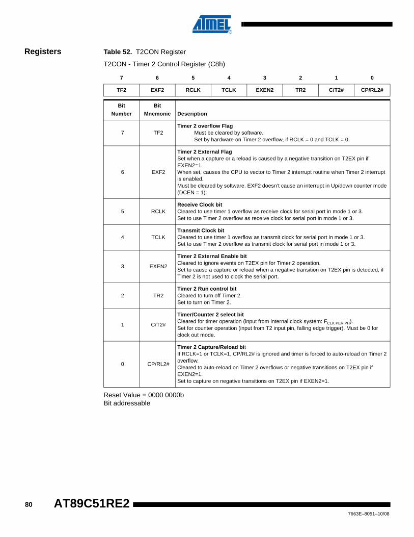
Registers Table 52. T2CON Register
T2CON - Timer 2 Control Register (C8h)
Reset Value = 0000 0000bBit addressable
7 6 5 4 3 2 1 0
TF2 EXF2 RCLK TCLK EXEN2 TR2 C/T2# CP/RL2#
Bit
Number
Bit
Mnemonic Description
7 TF2Timer 2 overflow Flag
Must be cleared by software. Set by hardware on Timer 2 overflow, if RCLK = 0 and TCLK = 0.
6 EXF2
Timer 2 External FlagSet when a capture or a reload is caused by a negative transition on T2EX pin if EXEN2=1.When set, causes the CPU to vector to Timer 2 interrupt routine when Timer 2 interrupt is enabled. Must be cleared by software. EXF2 doesn’t cause an interrupt in Up/down counter mode (DCEN = 1).
5 RCLKReceive Clock bitCleared to use timer 1 overflow as receive clock for serial port in mode 1 or 3.Set to use Timer 2 overflow as receive clock for serial port in mode 1 or 3.
4 TCLKTransmit Clock bitCleared to use timer 1 overflow as transmit clock for serial port in mode 1 or 3.Set to use Timer 2 overflow as transmit clock for serial port in mode 1 or 3.
3 EXEN2
Timer 2 External Enable bitCleared to ignore events on T2EX pin for Timer 2 operation. Set to cause a capture or reload when a negative transition on T2EX pin is detected, if Timer 2 is not used to clock the serial port.
2 TR2Timer 2 Run control bitCleared to turn off Timer 2.Set to turn on Timer 2.
1 C/T2#
Timer/Counter 2 select bitCleared for timer operation (input from internal clock system: FCLK PERIPH). Set for counter operation (input from T2 input pin, falling edge trigger). Must be 0 for clock out mode.
0 CP/RL2#
Timer 2 Capture/Reload bitIf RCLK=1 or TCLK=1, CP/RL2# is ignored and timer is forced to auto-reload on Timer 2 overflow. Cleared to auto-reload on Timer 2 overflows or negative transitions on T2EX pin if EXEN2=1.Set to capture on negative transitions on T2EX pin if EXEN2=1.
807663E–8051–10/08
AT89C51RE2

AT89C51RE2
Table 53. T2MOD Register
T2MOD - Timer 2 Mode Control Register (C9h)
Reset Value = XXXX XX00bNot bit addressable
7 6 5 4 3 2 1 0
- - - - - - T2OE DCEN
Bit
Number
Bit
Mnemonic Description
7 -ReservedThe value read from this bit is indeterminate. Do not set this bit.
6 -ReservedThe value read from this bit is indeterminate. Do not set this bit.
5 -ReservedThe value read from this bit is indeterminate. Do not set this bit.
4 -ReservedThe value read from this bit is indeterminate. Do not set this bit.
3 -ReservedThe value read from this bit is indeterminate. Do not set this bit.
2 -ReservedThe value read from this bit is indeterminate. Do not set this bit.
1 T2OETimer 2 Output Enable bitCleared to program P1.0/T2 as clock input or I/O port. Set to program P1.0/T2 as clock output.
0 DCENDown Counter Enable bitCleared to disable Timer 2 as up/down counter. Set to enable Timer 2 as up/down counter.
817663E–8051–10/08

Programmable Counter Array PCA
The PCA provides more timing capabilities with less CPU intervention than the standardtimer/counters. Its advantages include reduced software overhead and improved accuracy. ThePCA consists of a dedicated timer/counter which serves as the time base for an array of fivecompare/capture modules. Its clock input can be programmed to count any one of the followingsignals:
• Peripheral clock frequency (FCLK PERIPH) ÷ 6
• Peripheral clock frequency (FCLK PERIPH) ÷ 2
• Timer 0 overflow
• External input on ECI (P1.2)
Each compare/capture modules can be programmed in any one of the following modes:
• Rising and/or falling edge capture
• Software timer
• High-speed output
• Pulse width modulator
Module 4 can also be programmed as a watchdog timer (See Section "PCA Watchdog Timer",page 93).
When the compare/capture modules are programmed in the capture mode, software timer, orhigh speed output mode, an interrupt can be generated when the module executes its function.All five modules plus the PCA timer overflow share one interrupt vector.
The PCA timer/counter and compare/capture modules share Port 1 for external I/O. These pinsare listed below. If the port is not used for the PCA, it can still be used for standard I/O.
The PCA timer is a common time base for all five modules (See Figure 30). The timer countsource is determined from the CPS1 and CPS0 bits in the CMOD register (Table 54) and can beprogrammed to run at:
• 1/6 the peripheral clock frequency (FCLK PERIPH) • 1/2 the peripheral clock frequency (FCLK PERIPH)• The Timer 0 overflow
• The input on the ECI pin (P1.2)
PCA component External I/O Pin
16-bit Counter P1.2 / ECI
16-bit Module 0 P1.3 / CEX0
16-bit Module 1 P1.4 / CEX1
16-bit Module 2 P1.5 / CEX2
16-bit Module 3 P1.6 / CEX3
827663E–8051–10/08
AT89C51RE2

AT89C51RE2
Figure 30. PCA Timer/Counter
CIDL CPS1 CPS0 ECF
ItCH CL
16 bit up/down counter
To PCAmodules
Fclk periph /6
Fclk periph / 2
T0 OVF
P1.2
Idle
CMOD0xD9WDTE
CF CRCCON0xD8CCF4 CCF3 CCF2 CCF1 CCF0
overflow
837663E–8051–10/08
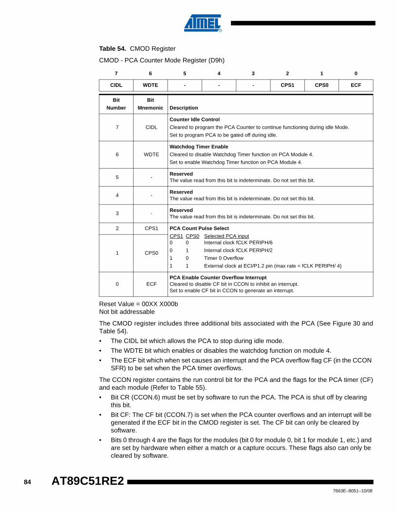
Table 54. CMOD Register
CMOD - PCA Counter Mode Register (D9h)
Reset Value = 00XX X000bNot bit addressable
The CMOD register includes three additional bits associated with the PCA (See Figure 30 andTable 54).
• The CIDL bit which allows the PCA to stop during idle mode.
• The WDTE bit which enables or disables the watchdog function on module 4.
• The ECF bit which when set causes an interrupt and the PCA overflow flag CF (in the CCON SFR) to be set when the PCA timer overflows.
The CCON register contains the run control bit for the PCA and the flags for the PCA timer (CF)and each module (Refer to Table 55).
• Bit CR (CCON.6) must be set by software to run the PCA. The PCA is shut off by clearing this bit.
• Bit CF: The CF bit (CCON.7) is set when the PCA counter overflows and an interrupt will be generated if the ECF bit in the CMOD register is set. The CF bit can only be cleared by software.
• Bits 0 through 4 are the flags for the modules (bit 0 for module 0, bit 1 for module 1, etc.) and are set by hardware when either a match or a capture occurs. These flags also can only be cleared by software.
7 6 5 4 3 2 1 0
CIDL WDTE - - - CPS1 CPS0 ECF
Bit
Number
Bit
Mnemonic Description
7 CIDL
Counter Idle Control
Cleared to program the PCA Counter to continue functioning during idle Mode.
Set to program PCA to be gated off during idle.
6 WDTE
Watchdog Timer Enable
Cleared to disable Watchdog Timer function on PCA Module 4.
Set to enable Watchdog Timer function on PCA Module 4.
5 -ReservedThe value read from this bit is indeterminate. Do not set this bit.
4 -ReservedThe value read from this bit is indeterminate. Do not set this bit.
3 -ReservedThe value read from this bit is indeterminate. Do not set this bit.
2 CPS1 PCA Count Pulse Select
CPS1 CPS0 Selected PCA input0 0 Internal clock fCLK PERIPH/6
0 1 Internal clock fCLK PERIPH/2
1 0 Timer 0 Overflow
1 1 External clock at ECI/P1.2 pin (max rate = fCLK PERIPH/ 4)
1 CPS0
0 ECFPCA Enable Counter Overflow InterruptCleared to disable CF bit in CCON to inhibit an interrupt.Set to enable CF bit in CCON to generate an interrupt.
847663E–8051–10/08
AT89C51RE2
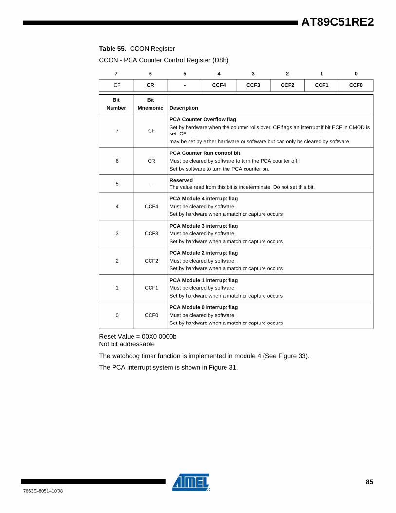
AT89C51RE2
Table 55. CCON Register
CCON - PCA Counter Control Register (D8h)
Reset Value = 00X0 0000bNot bit addressable
The watchdog timer function is implemented in module 4 (See Figure 33).
The PCA interrupt system is shown in Figure 31.
7 6 5 4 3 2 1 0
CF CR - CCF4 CCF3 CCF2 CCF1 CCF0
Bit
Number
Bit
Mnemonic Description
7 CF
PCA Counter Overflow flag
Set by hardware when the counter rolls over. CF flags an interrupt if bit ECF in CMOD is set. CF
may be set by either hardware or software but can only be cleared by software.
6 CR
PCA Counter Run control bit
Must be cleared by software to turn the PCA counter off.
Set by software to turn the PCA counter on.
5 -ReservedThe value read from this bit is indeterminate. Do not set this bit.
4 CCF4
PCA Module 4 interrupt flag
Must be cleared by software.
Set by hardware when a match or capture occurs.
3 CCF3
PCA Module 3 interrupt flag
Must be cleared by software.
Set by hardware when a match or capture occurs.
2 CCF2
PCA Module 2 interrupt flag
Must be cleared by software.
Set by hardware when a match or capture occurs.
1 CCF1
PCA Module 1 interrupt flag
Must be cleared by software.
Set by hardware when a match or capture occurs.
0 CCF0
PCA Module 0 interrupt flag
Must be cleared by software.
Set by hardware when a match or capture occurs.
857663E–8051–10/08
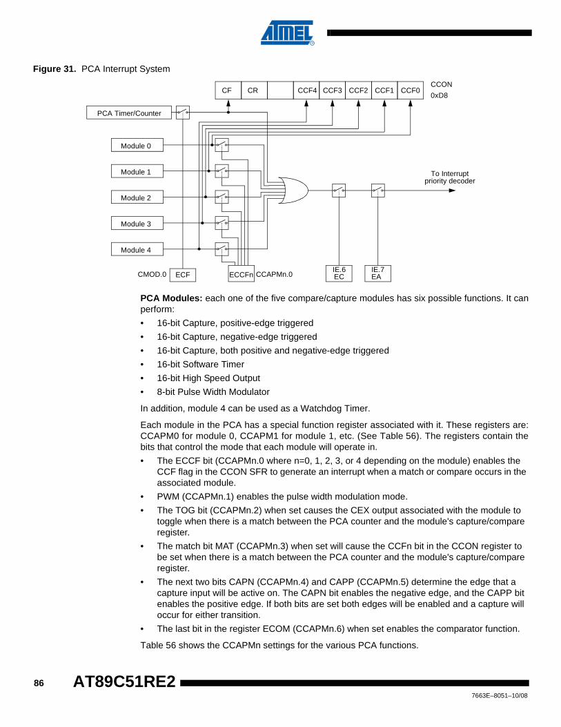
Figure 31. PCA Interrupt System
PCA Modules: each one of the five compare/capture modules has six possible functions. It canperform:
• 16-bit Capture, positive-edge triggered
• 16-bit Capture, negative-edge triggered
• 16-bit Capture, both positive and negative-edge triggered
• 16-bit Software Timer
• 16-bit High Speed Output
• 8-bit Pulse Width Modulator
In addition, module 4 can be used as a Watchdog Timer.
Each module in the PCA has a special function register associated with it. These registers are:CCAPM0 for module 0, CCAPM1 for module 1, etc. (See Table 56). The registers contain thebits that control the mode that each module will operate in.
• The ECCF bit (CCAPMn.0 where n=0, 1, 2, 3, or 4 depending on the module) enables the CCF flag in the CCON SFR to generate an interrupt when a match or compare occurs in the associated module.
• PWM (CCAPMn.1) enables the pulse width modulation mode.
• The TOG bit (CCAPMn.2) when set causes the CEX output associated with the module to toggle when there is a match between the PCA counter and the module's capture/compare register.
• The match bit MAT (CCAPMn.3) when set will cause the CCFn bit in the CCON register to be set when there is a match between the PCA counter and the module's capture/compare register.
• The next two bits CAPN (CCAPMn.4) and CAPP (CCAPMn.5) determine the edge that a capture input will be active on. The CAPN bit enables the negative edge, and the CAPP bit enables the positive edge. If both bits are set both edges will be enabled and a capture will occur for either transition.
• The last bit in the register ECOM (CCAPMn.6) when set enables the comparator function.
Table 56 shows the CCAPMn settings for the various PCA functions.
CF CRCCON
0xD8CCF4 CCF3 CCF2 CCF1 CCF0
Module 4
Module 3
Module 2
Module 1
Module 0
ECF
PCA Timer/Counter
ECCFn CCAPMn.0CMOD.0IE.6 IE.7
To Interruptpriority decoder
EC EA
867663E–8051–10/08
AT89C51RE2
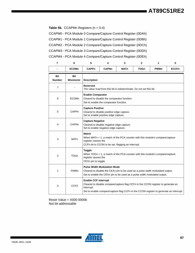
AT89C51RE2
Table 56. CCAPMn Registers (n = 0-4)
CCAPM0 - PCA Module 0 Compare/Capture Control Register (0DAh)
CCAPM1 - PCA Module 1 Compare/Capture Control Register (0DBh)
CCAPM2 - PCA Module 2 Compare/Capture Control Register (0DCh)
CCAPM3 - PCA Module 3 Compare/Capture Control Register (0DDh)
CCAPM4 - PCA Module 4 Compare/Capture Control Register (0DEh)
Reset Value = X000 0000bNot bit addressable
7 6 5 4 3 2 1 0
- ECOMn CAPPn CAPNn MATn TOGn PWMn ECCFn
Bit
Number
Bit
Mnemonic Description
7 -ReservedThe value read from this bit is indeterminate. Do not set this bit.
6 ECOMn
Enable Comparator
Cleared to disable the comparator function.
Set to enable the comparator function.
5 CAPPnCapture Positive
Cleared to disable positive edge capture.Set to enable positive edge capture.
4 CAPNnCapture Negative
Cleared to disable negative edge capture.Set to enable negative edge capture.
3 MATn
Match
When MATn = 1, a match of the PCA counter with this module's compare/capture register causes the
CCFn bit in CCON to be set, flagging an interrupt.
2 TOGn
Toggle
When TOGn = 1, a match of the PCA counter with this module's compare/capture register causes the
CEXn pin to toggle.
1 PWMn
Pulse Width Modulation Mode
Cleared to disable the CEXn pin to be used as a pulse width modulated output.
Set to enable the CEXn pin to be used as a pulse width modulated output.
0 CCF0
Enable CCF interrupt
Cleared to disable compare/capture flag CCFn in the CCON register to generate an interrupt.
Set to enable compare/capture flag CCFn in the CCON register to generate an interrupt.
877663E–8051–10/08
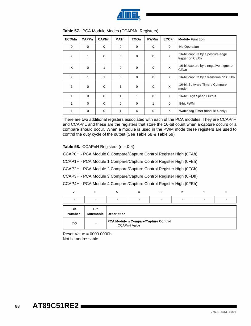
Table 57. PCA Module Modes (CCAPMn Registers)
There are two additional registers associated with each of the PCA modules. They are CCAPnHand CCAPnL and these are the registers that store the 16-bit count when a capture occurs or acompare should occur. When a module is used in the PWM mode these registers are used tocontrol the duty cycle of the output (See Table 58 & Table 59).
Table 58. CCAPnH Registers (n = 0-4)
CCAP0H - PCA Module 0 Compare/Capture Control Register High (0FAh)
CCAP1H - PCA Module 1 Compare/Capture Control Register High (0FBh)
CCAP2H - PCA Module 2 Compare/Capture Control Register High (0FCh)
CCAP3H - PCA Module 3 Compare/Capture Control Register High (0FDh)
CCAP4H - PCA Module 4 Compare/Capture Control Register High (0FEh)
Reset Value = 0000 0000bNot bit addressable
ECOMn CAPPn CAPNn MATn TOGn PWMm ECCFn Module Function
0 0 0 0 0 0 0 No Operation
X 1 0 0 0 0 X 16-bit capture by a positive-edge trigger on CEXn
X 0 1 0 0 0 X 16-bit capture by a negative trigger on CEXn
X 1 1 0 0 0 X 16-bit capture by a transition on CEXn
1 0 0 1 0 0 X 16-bit Software Timer / Compare mode.
1 0 0 1 1 0 X 16-bit High Speed Output
1 0 0 0 0 1 0 8-bit PWM
1 0 0 1 X 0 X Watchdog Timer (module 4 only)
7 6 5 4 3 2 1 0
- - - - - - - -
Bit
Number
Bit
Mnemonic Description
7-0 -PCA Module n Compare/Capture Control
CCAPnH Value
887663E–8051–10/08
AT89C51RE2
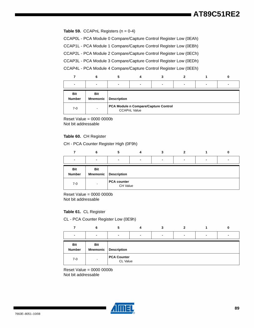
AT89C51RE2
Table 59. CCAPnL Registers (n = 0-4)
CCAP0L - PCA Module 0 Compare/Capture Control Register Low (0EAh)
CCAP1L - PCA Module 1 Compare/Capture Control Register Low (0EBh)
CCAP2L - PCA Module 2 Compare/Capture Control Register Low (0ECh)
CCAP3L - PCA Module 3 Compare/Capture Control Register Low (0EDh)
CCAP4L - PCA Module 4 Compare/Capture Control Register Low (0EEh)
Reset Value = 0000 0000bNot bit addressable
Table 60. CH Register
CH - PCA Counter Register High (0F9h)
Reset Value = 0000 0000bNot bit addressable
Table 61. CL Register
CL - PCA Counter Register Low (0E9h)
Reset Value = 0000 0000bNot bit addressable
7 6 5 4 3 2 1 0
- - - - - - - -
Bit
Number
Bit
Mnemonic Description
7-0 -PCA Module n Compare/Capture Control
CCAPnL Value
7 6 5 4 3 2 1 0
- - - - - - - -
Bit
Number
Bit
Mnemonic Description
7-0 -PCA counter
CH Value
7 6 5 4 3 2 1 0
- - - - - - - -
Bit
Number
Bit
Mnemonic Description
7-0 -PCA Counter
CL Value
897663E–8051–10/08
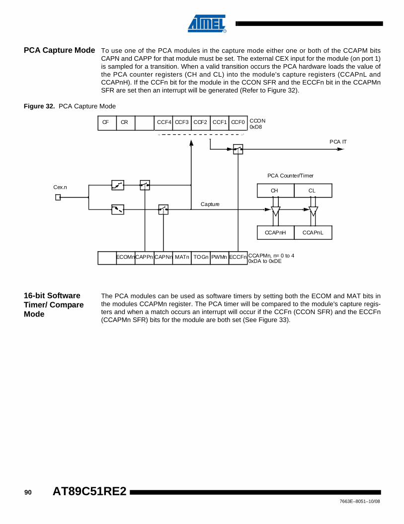
PCA Capture Mode To use one of the PCA modules in the capture mode either one or both of the CCAPM bitsCAPN and CAPP for that module must be set. The external CEX input for the module (on port 1)is sampled for a transition. When a valid transition occurs the PCA hardware loads the value ofthe PCA counter registers (CH and CL) into the module's capture registers (CCAPnL andCCAPnH). If the CCFn bit for the module in the CCON SFR and the ECCFn bit in the CCAPMnSFR are set then an interrupt will be generated (Refer to Figure 32).
Figure 32. PCA Capture Mode
16-bit Software Timer/ Compare Mode
The PCA modules can be used as software timers by setting both the ECOM and MAT bits inthe modules CCAPMn register. The PCA timer will be compared to the module's capture regis-ters and when a match occurs an interrupt will occur if the CCFn (CCON SFR) and the ECCFn(CCAPMn SFR) bits for the module are both set (See Figure 33).
CF CR CCON0xD8
CH CL
CCAPnH CCAPnL
CCF4 CCF3 CCF2 CCF1 CCF0
PCA IT
PCA Counter/Timer
ECOMn CCAPMn, n= 0 to 40xDA to 0xDE
CAPNn MATn TOGn PWMn ECCFnCAPPn
Cex.n
Capture
907663E–8051–10/08
AT89C51RE2
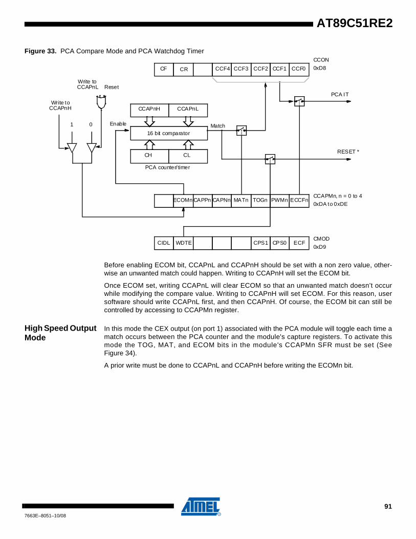
AT89C51RE2
Figure 33. PCA Compare Mode and PCA Watchdog Timer
Before enabling ECOM bit, CCAPnL and CCAPnH should be set with a non zero value, other-wise an unwanted match could happen. Writing to CCAPnH will set the ECOM bit.
Once ECOM set, writing CCAPnL will clear ECOM so that an unwanted match doesn’t occurwhile modifying the compare value. Writing to CCAPnH will set ECOM. For this reason, usersoftware should write CCAPnL first, and then CCAPnH. Of course, the ECOM bit can still becontrolled by accessing to CCAPMn register.
High Speed Output Mode
In this mode the CEX output (on port 1) associated with the PCA module will toggle each time amatch occurs between the PCA counter and the module's capture registers. To activate thismode the TOG, MAT, and ECOM bits in the module's CCAPMn SFR must be set (SeeFigure 34).
A prior write must be done to CCAPnL and CCAPnH before writing the ECOMn bit.
CH CL
CCAPnH CCAPnL
ECOMnCCAPMn, n = 0 to 4
0xDA to 0xDECAPNn MATn TOGn PWMn ECCFnCAPPn
16 bit comparatorMatch
CCON
0xD8
PCA IT
Enable
PCA counter/ timer
RESET *
CIDL CPS1 CPS0 ECFCMOD
0xD9WDTE
ResetWrite toCCAPnL
Write toCCAPnH
CF CCF2 CCF1 CCF0CR CCF3CCF4
1 0
917663E–8051–10/08
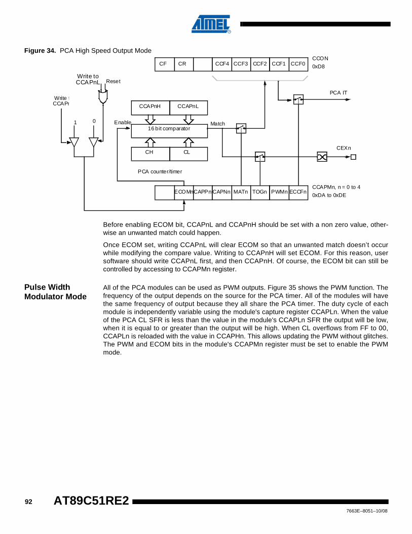
Figure 34. PCA High Speed Output Mode
Before enabling ECOM bit, CCAPnL and CCAPnH should be set with a non zero value, other-wise an unwanted match could happen.
Once ECOM set, writing CCAPnL will clear ECOM so that an unwanted match doesn’t occurwhile modifying the compare value. Writing to CCAPnH will set ECOM. For this reason, usersoftware should write CCAPnL first, and then CCAPnH. Of course, the ECOM bit can still becontrolled by accessing to CCAPMn register.
Pulse Width Modulator Mode
All of the PCA modules can be used as PWM outputs. Figure 35 shows the PWM function. Thefrequency of the output depends on the source for the PCA timer. All of the modules will havethe same frequency of output because they all share the PCA timer. The duty cycle of eachmodule is independently variable using the module's capture register CCAPLn. When the valueof the PCA CL SFR is less than the value in the module's CCAPLn SFR the output will be low,when it is equal to or greater than the output will be high. When CL overflows from FF to 00,CCAPLn is reloaded with the value in CCAPHn. This allows updating the PWM without glitches.The PWM and ECOM bits in the module's CCAPMn register must be set to enable the PWMmode.
CH CL
CCAPnH CCAPnL
ECOMnCCAPMn, n = 0 to 4
0xDA to 0xDECAPNn MATn TOGn PWMn ECCFnCAPPn
16 bit comparatorMatch
CF CRCCON
0xD8CCF4 CCF3 CCF2 CCF1 CCF0
PCA IT
Enable
CEXn
PCA counter/timer
Write toCCAPnH
ResetWrite toCCAPnL
1 0
927663E–8051–10/08
AT89C51RE2

AT89C51RE2
Figure 35. PCA PWM Mode
PCA Watchdog Timer
An on-board watchdog timer is available with the PCA to improve the reliability of the systemwithout increasing chip count. Watchdog timers are useful for systems that are susceptible tonoise, power glitches, or electrostatic discharge. Module 4 is the only PCA module that can beprogrammed as a watchdog. However, this module can still be used for other modes if thewatchdog is not needed. Figure 33 shows a diagram of how the watchdog works. The user pre-loads a 16-bit value in the compare registers. Just like the other compare modes, this 16-bitvalue is compared to the PCA timer value. If a match is allowed to occur, an internal reset will begenerated. This will not cause the RST pin to be driven high.
In order to hold off the reset, the user has three options:
1. periodically change the compare value so it will never match the PCA timer,
2. periodically change the PCA timer value so it will never match the compare values, or
3. disable the watchdog by clearing the WDTE bit before a match occurs and then re-enable it.
The first two options are more reliable because the watchdog timer is never disabled as in option#3. If the program counter ever goes astray, a match will eventually occur and cause an internalreset. The second option is also not recommended if other PCA modules are being used.Remember, the PCA timer is the time base for all modules; changing the time base for othermodules would not be a good idea. Thus, in most applications the first solution is the best option.
This watchdog timer won’t generate a reset out on the reset pin.
CL
CCAPnH
CCAPnL
ECOMn CCAPMn, n= 0 to 4
0xDA to 0xDECAPNn MATn TOGn PWMn ECCFnCAPPn
8 bit comparatorCEXn
“0”
“1”
Enable
PCA counter/timer
Overflow
937663E–8051–10/08
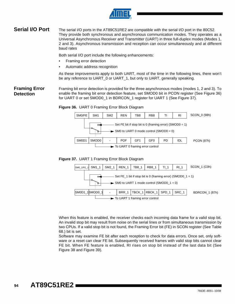
Serial I/O Port The serial I/O ports in the AT89C51RE2 are compatible with the serial I/O port in the 80C52.They provide both synchronous and asynchronous communication modes. They operates as aUniversal Asynchronous Receiver and Transmitter (UART) in three full-duplex modes (Modes 1,2 and 3). Asynchronous transmission and reception can occur simultaneously and at differentbaud rates
Both serial I/O port include the following enhancements:
• Framing error detection
• Automatic address recognition
As these improvements apply to both UART, most of the time in the following lines, there won’tbe any reference to UART_0 or UART_1, but only to UART, generally speaking.
Framing Error Detection
Framing bit error detection is provided for the three asynchronous modes (modes 1, 2 and 3). Toenable the framing bit error detection feature, set SMOD0 bit in PCON register (See Figure 36)for UART 0 or set SMOD0_1 in BDRCON_1 register for UART 1 (See Figure 37).
Figure 36. UART 0 Framing Error Block Diagram
Figure 37. UART 1 Framing Error Block Diagram
When this feature is enabled, the receiver checks each incoming data frame for a valid stop bit.An invalid stop bit may result from noise on the serial lines or from simultaneous transmission bytwo CPUs. If a valid stop bit is not found, the Framing Error bit (FE) in SCON register (See Table68.) bit is set. Software may examine FE bit after each reception to check for data errors. Once set, only soft-ware or a reset can clear FE bit. Subsequently received frames with valid stop bits cannot clearFE bit. When FE feature is enabled, RI rises on stop bit instead of the last data bit (SeeFigure 38 and Figure 39).
To UART 0 framing error control
SM0 to UART 0 mode control (SMOD0 = 0)
Set FE bit if stop bit is 0 (framing error) (SMOD0 = 1)
SCON_0 (98h)
PCON (87h)
SM0/FE SM1 SM2 REN TB8 RB8 TI RI
SM0D1 SMOD0 - POF GF1 GF0 PD IDL
To UART 1 framing error control
SM0 to UART 1 mode control (SMOD0_1 = 0)
Set FE_1 bit if stop bit is 0 (framing error) (SMOD0_1 = 1)
SCON_1 (C0h)
BDRCON_1 (87h)
SM0_1/FE_1 SM1_1 SM2_1 REN_1 TB8_1 RB8_1 TI_1 RI_1
SM0D1_1SMOD0_1 - BRR_1 TBCK_1 RBCK_1 SPD_1 SRC_1
947663E–8051–10/08
AT89C51RE2
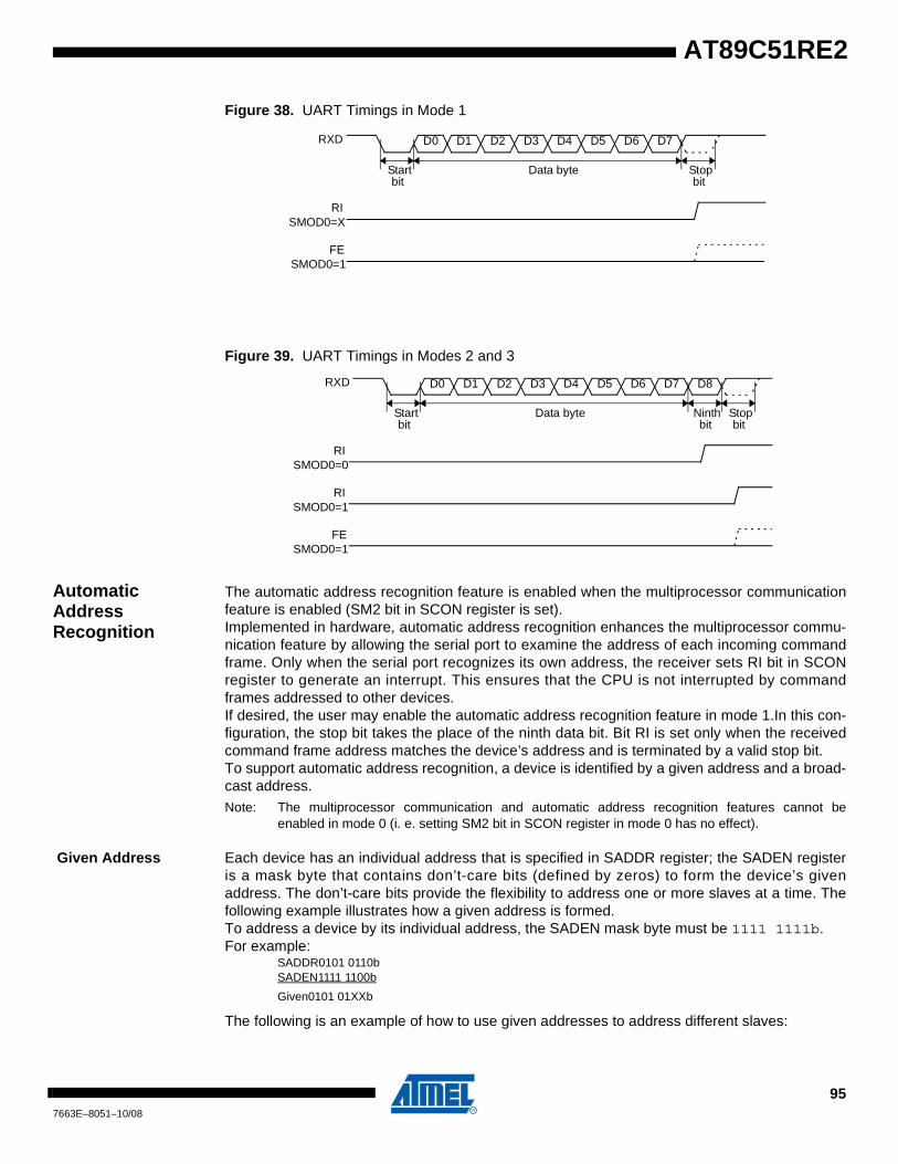
AT89C51RE2
Figure 38. UART Timings in Mode 1
Figure 39. UART Timings in Modes 2 and 3
Automatic Address Recognition
The automatic address recognition feature is enabled when the multiprocessor communicationfeature is enabled (SM2 bit in SCON register is set). Implemented in hardware, automatic address recognition enhances the multiprocessor commu-nication feature by allowing the serial port to examine the address of each incoming commandframe. Only when the serial port recognizes its own address, the receiver sets RI bit in SCONregister to generate an interrupt. This ensures that the CPU is not interrupted by commandframes addressed to other devices. If desired, the user may enable the automatic address recognition feature in mode 1.In this con-figuration, the stop bit takes the place of the ninth data bit. Bit RI is set only when the receivedcommand frame address matches the device’s address and is terminated by a valid stop bit. To support automatic address recognition, a device is identified by a given address and a broad-cast address. Note: The multiprocessor communication and automatic address recognition features cannot be
enabled in mode 0 (i. e. setting SM2 bit in SCON register in mode 0 has no effect).
Given Address Each device has an individual address that is specified in SADDR register; the SADEN registeris a mask byte that contains don’t-care bits (defined by zeros) to form the device’s givenaddress. The don’t-care bits provide the flexibility to address one or more slaves at a time. Thefollowing example illustrates how a given address is formed. To address a device by its individual address, the SADEN mask byte must be 1111 1111b. For example:
SADDR0101 0110bSADEN1111 1100b
Given0101 01XXb
The following is an example of how to use given addresses to address different slaves:
Data byte
RISMOD0=X
Stopbit
Startbit
RXD D7D6D5D4D3D2D1D0
FESMOD0=1
RISMOD0=0
Data byte Ninthbit
Stopbit
Startbit
RXD D8D7D6D5D4D3D2D1D0
RISMOD0=1
FESMOD0=1
957663E–8051–10/08
Slave A:SADDR1111 0001bSADEN1111 1010b
Given1111 0X0Xb
Slave B:SADDR1111 0011bSADEN1111 1001b
Given1111 0XX1b
Slave C:SADDR1111 0010bSADEN1111 1101b
Given1111 00X1b
The SADEN byte is selected so that each slave may be addressed separately. For slave A, bit 0 (the LSB) is a don’t-care bit; for slaves B and C, bit 0 is a 1.To communicatewith slave A only, the master must send an address where bit 0 is clear (e.g.. 1111 0000b). For slave A, bit 1 is a 1; for slaves B and C, bit 1 is a don’t care bit. To communicate with slavesB and C, but not slave A, the master must send an address with bits 0 and 1 both set (e.g. 11110011b). To communicate with slaves A, B and C, the master must send an address with bit 0 set, bit 1clear, and bit 2 clear (e.g. 1111 0001b).
Broadcast Address A broadcast address is formed from the logical OR of the SADDR and SADEN registers withzeros defined as don’t-care bits, e.g.:
SADDR0101 0110bSADEN1111 1100b
Broadcast =SADDR OR SADEN1111 111Xb
The use of don’t-care bits provides flexibility in defining the broadcast address, however in mostapplications, a broadcast address is FFh. The following is an example of using broadcastaddresses:
Slave A:SADDR1111 0001bSADEN1111 1010b
Broadcast1111 1X11b,
Slave B:SADDR1111 0011bSADEN1111 1001b
Broadcast1111 1X11B,
Slave C:SADDR=1111 0011bSADEN1111 1101b
Broadcast1111 1111b
For slaves A and B, bit 2 is a don’t care bit; for slave C, bit 2 is set. To communicate with all ofthe slaves, the master must send an address FFh. To communicate with slaves A and B, but notslave C, the master can send and address FBh.
Reset Addresses On reset, the SADDR and SADEN registers are initialized to 00h, i. e. the given and broadcastaddresses are XXXX XXXXb (all don’t-care bits). This ensures that the serial port will reply to anyaddress, and so, that it is backwards compatible with the 80C51 microcontrollers that do notsupport automatic address recognition.
967663E–8051–10/08
AT89C51RE2
AT89C51RE2
Registers Table 62. SADEN_0 Register
SADEN - Slave Address Mask Register UART 0(B9h)
Reset Value = 0000 0000bNot bit addressable
Table 63. SADDR_0 Register
SADDR - Slave Address Register UART 0(A9h)
Reset Value = 0000 0000bNot bit addressable
Table 64. SADEN_1 Register
SADEN_1 - Slave Address Mask Register UART 1(BAh)
Reset Value = 0000 0000bNot bit addressable
Table 65. SADDR_1 Register
SADDR_1 - Slave Address Register UART 1(AAh)
Reset Value = 0000 0000bNot bit addressable
7 6 5 4 3 2 1 0
7 6 5 4 3 2 1 0
7 6 5 4 3 2 1 0
7 6 5 4 3 2 1 0
977663E–8051–10/08

Baud Rate Selection for UART 0 for Mode 1 and 3
The Baud Rate Generator for transmit and receive clocks can be selected separately via theT2CON and BDRCON_0 registers.
Figure 40. Baud Rate Selection for UART 0
Table 66. Baud Rate Selection Table UART 0
TCLK
(T2CON)
RCLK
(T2CON)
TBCK
(BDRCON)
RBCK
(BDRCON)
Clock Source
UART Tx
Clock Source
UART Rx
0 0 0 0 Timer 1 Timer 1
1 0 0 0 Timer 2 Timer 1
0 1 0 0 Timer 1 Timer 2
1 1 0 0 Timer 2 Timer 2
X 0 1 0 INT_BRG Timer 1
X 1 1 0 INT_BRG Timer 2
0 X 0 1 Timer 1 INT_BRG
1 X 0 1 Timer 2 INT_BRG
X X 1 1 INT_BRG INT_BRG
RCLK
/ 16
RBCKINT_BRG
0
1
TIMER1
0
1
0
1TIMER2
INT_BRG
TIMER1
TIMER2
TIMER_BRG_RX
Rx Clock_0
/ 160
1
TIMER_BRG_TX
Tx Clock_0
TBCK
TCLK
987663E–8051–10/08
AT89C51RE2
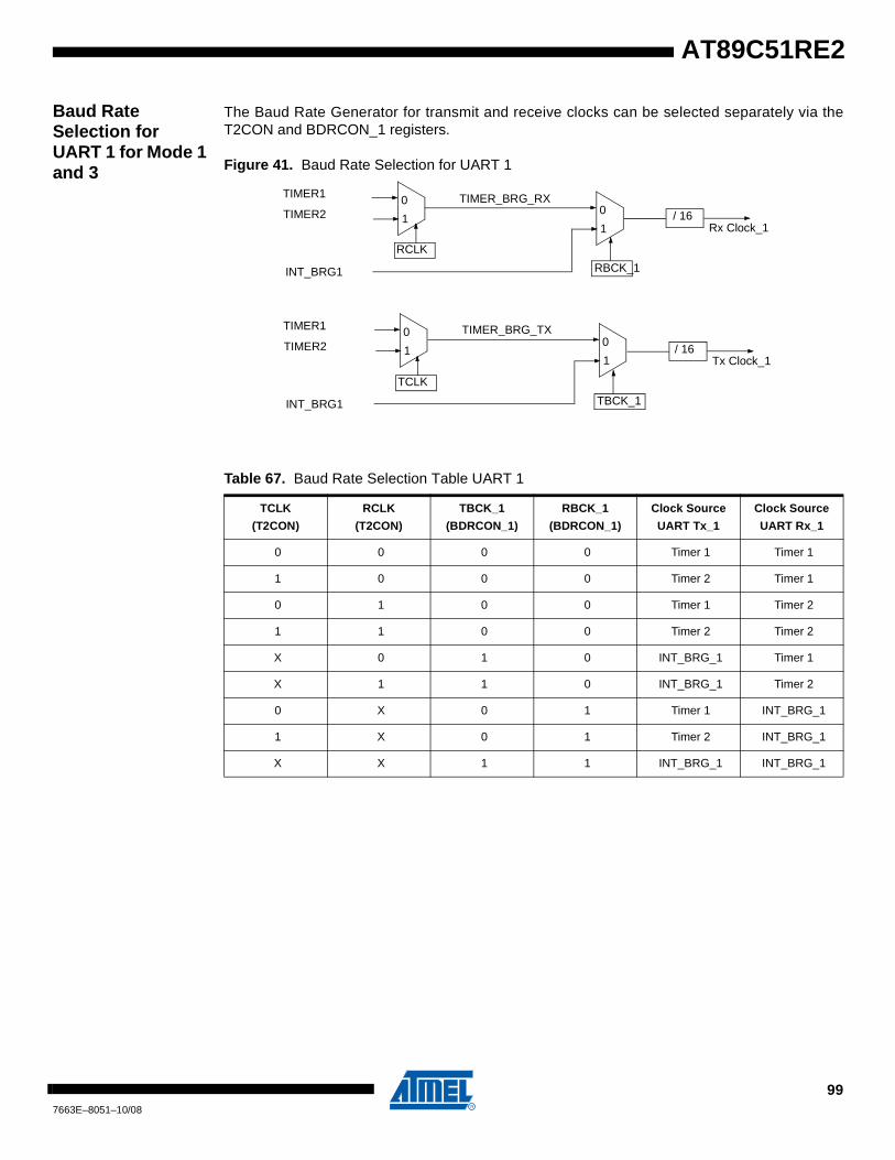
AT89C51RE2
Baud Rate Selection for UART 1 for Mode 1 and 3
The Baud Rate Generator for transmit and receive clocks can be selected separately via theT2CON and BDRCON_1 registers.
Figure 41. Baud Rate Selection for UART 1
Table 67. Baud Rate Selection Table UART 1
TCLK
(T2CON)
RCLK
(T2CON)
TBCK_1
(BDRCON_1)
RBCK_1
(BDRCON_1)
Clock Source
UART Tx_1
Clock Source
UART Rx_1
0 0 0 0 Timer 1 Timer 1
1 0 0 0 Timer 2 Timer 1
0 1 0 0 Timer 1 Timer 2
1 1 0 0 Timer 2 Timer 2
X 0 1 0 INT_BRG_1 Timer 1
X 1 1 0 INT_BRG_1 Timer 2
0 X 0 1 Timer 1 INT_BRG_1
1 X 0 1 Timer 2 INT_BRG_1
X X 1 1 INT_BRG_1 INT_BRG_1
RCLK
/ 16
RBCK_1INT_BRG1
0
1
TIMER1
0
1
0
1TIMER2
INT_BRG1
TIMER1
TIMER2
TIMER_BRG_RX
Rx Clock_1
/ 160
1
TIMER_BRG_TX
Tx Clock_1
TBCK_1
TCLK
997663E–8051–10/08
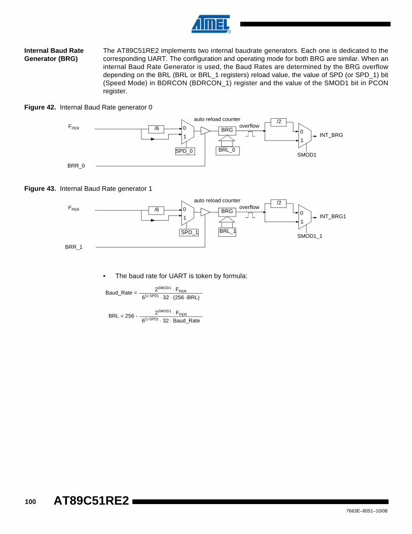
Internal Baud Rate Generator (BRG)
The AT89C51RE2 implements two internal baudrate generators. Each one is dedicated to thecorresponding UART. The configuration and operating mode for both BRG are similar. When aninternal Baud Rate Generator is used, the Baud Rates are determined by the BRG overflowdepending on the BRL (BRL or BRL_1 registers) reload value, the value of SPD (or SPD_1) bit(Speed Mode) in BDRCON (BDRCON_1) register and the value of the SMOD1 bit in PCONregister.
Figure 42. Internal Baud Rate generator 0
Figure 43. Internal Baud Rate generator 1
• The baud rate for UART is token by formula:
SPD_0
BRG0
1
/6
BRL_0
/2
0
1INT_BRG
BRR_0
SMOD1
auto reload counteroverflowFPER
BRG0
1
/6
BRL_1
/2
0
1INT_BRG1
SPD_1
BRR_1
SMOD1_1
auto reload counteroverflowFPER
Baud_Rate =6(1-SPD) ⋅ 32 ⋅ (256 -BRL)
2SMOD1 ⋅ FPER
BRL = 256 -6(1-SPD) ⋅ 32 ⋅ Baud_Rate
2SMOD1 ⋅ FPER
1007663E–8051–10/08
AT89C51RE2

AT89C51RE2
Table 68. SCON_0 register
SCON_0 - Serial Control Register for UART 0(98h)
Reset Value = 0000 0000bBit addressable
7 6 5 4 3 2 1 0
FE/SM0_0 SM1_0 SM2_0 REN_0 TB8_0 RB8_0 TI_0 RI_0
Bit
Number
Bit
Mnemonic Description
7
FE_0
Framing Error bit (SMOD0=1)
Clear to reset the error state, not cleared by a valid stop bit. Set by hardware when an invalid stop bit is detected.
SMOD0 must be set to enable access to the FE bit.
SM0_0Serial port Mode bit 0Refer to SM1_0 for serial port mode selection.
SMOD0_0 must be cleared to enable access to the SM0_0 bit.
6 SM1_0
Serial port Mode bit 1SM0 SM1 Mode Description Baud Rate
0 0 0 Shift Register FCPU PERIPH/6 0 1 1 8-bit UART Variable1 0 2 9-bit UART FCPU PERIPH /32 or /16
1 1 3 9-bit UART Variable
5 SM2_0
Serial port Mode 2 bit / Multiprocessor Communication Enable bit
Clear to disable multiprocessor communication feature.
Set to enable multiprocessor communication feature in mode 2 and 3, and eventually mode 1.This bit should be cleared in mode 0.
4 REN_0Reception Enable bitClear to disable serial reception. Set to enable serial reception.
3 TB8_0Transmitter Bit 8 / Ninth bit to transmit in modes 2 and 3
Clear to transmit a logic 0 in the 9th bit. Set to transmit a logic 1 in the 9th bit.
2 RB8_0
Receiver Bit 8 / Ninth bit received in modes 2 and 3Cleared by hardware if 9th bit received is a logic 0.Set by hardware if 9th bit received is a logic 1.
In mode 1, if SM2_0 = 0, RB8 is the received stop bit. In mode 0 RB8 is not used.
1 TI_0
Transmit Interrupt flagClear to acknowledge interrupt. Set by hardware at the end of the 8th bit time in mode 0 or at the beginning of the stop bit in the other modes.
0 RI_0
Receive Interrupt flagClear to acknowledge interrupt. Set by hardware at the end of the 8th bit time in mode 0, see Figure 38. and Figure 39. in the other modes.
1017663E–8051–10/08
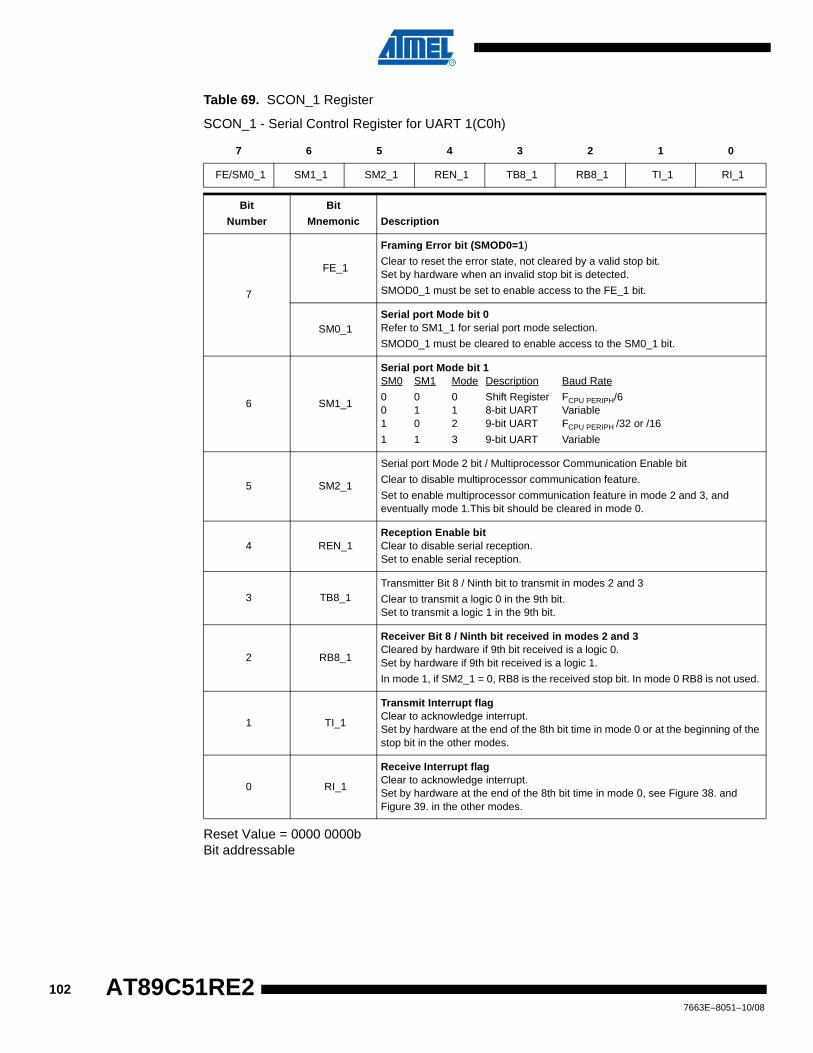
Table 69. SCON_1 Register
SCON_1 - Serial Control Register for UART 1(C0h)
Reset Value = 0000 0000bBit addressable
7 6 5 4 3 2 1 0
FE/SM0_1 SM1_1 SM2_1 REN_1 TB8_1 RB8_1 TI_1 RI_1
Bit
Number
Bit
Mnemonic Description
7
FE_1
Framing Error bit (SMOD0=1)
Clear to reset the error state, not cleared by a valid stop bit. Set by hardware when an invalid stop bit is detected.
SMOD0_1 must be set to enable access to the FE_1 bit.
SM0_1Serial port Mode bit 0Refer to SM1_1 for serial port mode selection.
SMOD0_1 must be cleared to enable access to the SM0_1 bit.
6 SM1_1
Serial port Mode bit 1SM0 SM1 Mode Description Baud Rate
0 0 0 Shift Register FCPU PERIPH/6 0 1 1 8-bit UART Variable1 0 2 9-bit UART FCPU PERIPH /32 or /16
1 1 3 9-bit UART Variable
5 SM2_1
Serial port Mode 2 bit / Multiprocessor Communication Enable bit
Clear to disable multiprocessor communication feature.
Set to enable multiprocessor communication feature in mode 2 and 3, and eventually mode 1.This bit should be cleared in mode 0.
4 REN_1Reception Enable bitClear to disable serial reception. Set to enable serial reception.
3 TB8_1Transmitter Bit 8 / Ninth bit to transmit in modes 2 and 3
Clear to transmit a logic 0 in the 9th bit. Set to transmit a logic 1 in the 9th bit.
2 RB8_1
Receiver Bit 8 / Ninth bit received in modes 2 and 3Cleared by hardware if 9th bit received is a logic 0.Set by hardware if 9th bit received is a logic 1.
In mode 1, if SM2_1 = 0, RB8 is the received stop bit. In mode 0 RB8 is not used.
1 TI_1
Transmit Interrupt flagClear to acknowledge interrupt. Set by hardware at the end of the 8th bit time in mode 0 or at the beginning of the stop bit in the other modes.
0 RI_1
Receive Interrupt flagClear to acknowledge interrupt. Set by hardware at the end of the 8th bit time in mode 0, see Figure 38. and Figure 39. in the other modes.
1027663E–8051–10/08
AT89C51RE2
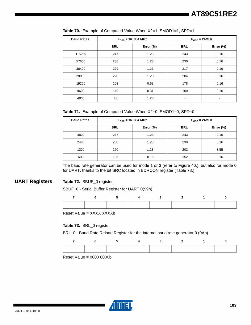
AT89C51RE2
Table 70. Example of Computed Value When X2=1, SMOD1=1, SPD=1
Table 71. Example of Computed Value When X2=0, SMOD1=0, SPD=0
The baud rate generator can be used for mode 1 or 3 (refer to Figure 40.), but also for mode 0for UART, thanks to the bit SRC located in BDRCON register (Table 78.)
UART Registers Table 72. SBUF_0 register
SBUF_0 - Serial Buffer Register for UART 0(99h)
Reset Value = XXXX XXXXb
Table 73. BRL_0 register
BRL_0 - Baud Rate Reload Register for the internal baud rate generator 0 (9Ah)
Reset Value = 0000 0000b
Baud Rates FOSC = 16. 384 MHz FOSC = 24MHz
BRL Error (%) BRL Error (%)
115200 247 1.23 243 0.16
57600 238 1.23 230 0.16
38400 229 1.23 217 0.16
28800 220 1.23 204 0.16
19200 203 0.63 178 0.16
9600 149 0.31 100 0.16
4800 43 1.23 - -
Baud Rates FOSC = 16. 384 MHz FOSC = 24MHz
BRL Error (%) BRL Error (%)
4800 247 1.23 243 0.16
2400 238 1.23 230 0.16
1200 220 1.23 202 3.55
600 185 0.16 152 0.16
7 6 5 4 3 2 1 0
7 6 5 4 3 2 1 0
1037663E–8051–10/08
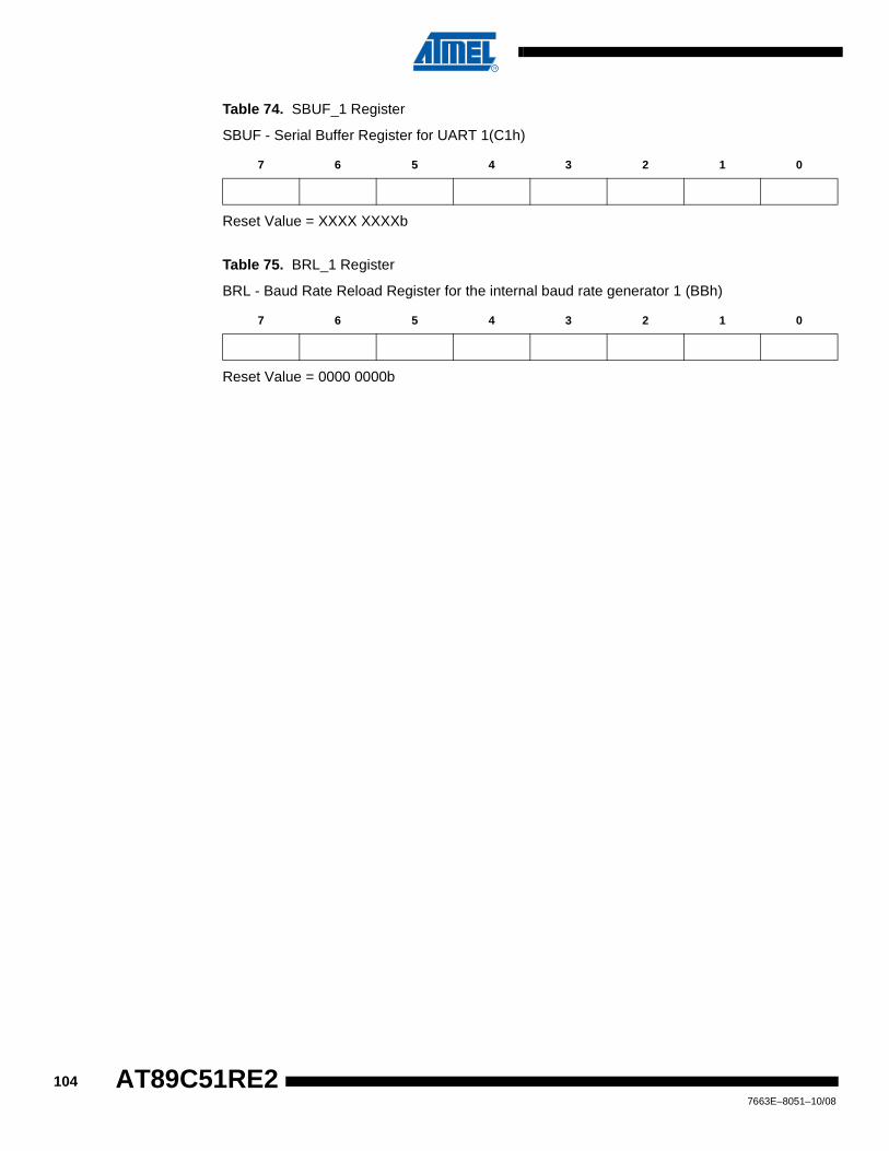
Table 74. SBUF_1 Register
SBUF - Serial Buffer Register for UART 1(C1h)
Reset Value = XXXX XXXXb
Table 75. BRL_1 Register
BRL - Baud Rate Reload Register for the internal baud rate generator 1 (BBh)
Reset Value = 0000 0000b
7 6 5 4 3 2 1 0
7 6 5 4 3 2 1 0
1047663E–8051–10/08
AT89C51RE2
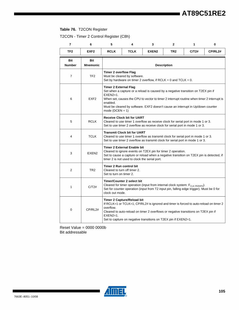
AT89C51RE2
Table 76. T2CON Register
T2CON - Timer 2 Control Register (C8h)
Reset Value = 0000 0000bBit addressable
7 6 5 4 3 2 1 0
TF2 EXF2 RCLK TCLK EXEN2 TR2 C/T2# CP/RL2#
Bit
Number
Bit
Mnemonic Description
7 TF2Timer 2 overflow FlagMust be cleared by software. Set by hardware on timer 2 overflow, if RCLK = 0 and TCLK = 0.
6 EXF2
Timer 2 External FlagSet when a capture or a reload is caused by a negative transition on T2EX pin if EXEN2=1.When set, causes the CPU to vector to timer 2 interrupt routine when timer 2 interrupt is enabled. Must be cleared by software. EXF2 doesn’t cause an interrupt in Up/down counter mode (DCEN = 1)
5 RCLKReceive Clock bit for UARTCleared to use timer 1 overflow as receive clock for serial port in mode 1 or 3.Set to use timer 2 overflow as receive clock for serial port in mode 1 or 3.
4 TCLKTransmit Clock bit for UARTCleared to use timer 1 overflow as transmit clock for serial port in mode 1 or 3.Set to use timer 2 overflow as transmit clock for serial port in mode 1 or 3.
3 EXEN2
Timer 2 External Enable bitCleared to ignore events on T2EX pin for timer 2 operation. Set to cause a capture or reload when a negative transition on T2EX pin is detected, if timer 2 is not used to clock the serial port.
2 TR2Timer 2 Run control bitCleared to turn off timer 2.Set to turn on timer 2.
1 C/T2#
Timer/Counter 2 select bitCleared for timer operation (input from internal clock system: FCLK PERIPH). Set for counter operation (input from T2 input pin, falling edge trigger). Must be 0 for clock out mode.
0 CP/RL2#
Timer 2 Capture/Reload bitIf RCLK=1 or TCLK=1, CP/RL2# is ignored and timer is forced to auto-reload on timer 2 overflow. Cleared to auto-reload on timer 2 overflows or negative transitions on T2EX pin if EXEN2=1.Set to capture on negative transitions on T2EX pin if EXEN2=1.
1057663E–8051–10/08

Table 77. PCON Register
PCON - Power Control Register (87h)
Reset Value = 00X1 0000bNot bit addressable
Power-off flag reset value will be 1 only after a power on (cold reset). A warm reset doesn’t affectthe value of this bit.
7 6 5 4 3 2 1 0
SMOD1_0 SMOD0_0 - POF GF1 GF0 PD IDL
Bit
Number
Bit
Mnemonic Description
7 SMOD1_0Serial port Mode bit 1 for UARTSet to select double baud rate in mode 1, 2 or 3.
6 SMOD0_0Serial port Mode bit 0 for UART
Cleared to select SM0 bit in SCON register. Set to select FE bit in SCON register.
5 -ReservedThe value read from this bit is indeterminate. Do not set this bit.
4 POF
Power-Off FlagCleared to recognize next reset type. Set by hardware when VCC rises from 0 to its nominal voltage. Can also be set by software.
3 GF1General purpose FlagCleared by user for general purpose usage. Set by user for general purpose usage.
2 GF0General purpose FlagCleared by user for general purpose usage. Set by user for general purpose usage.
1 PDPower-Down mode bitCleared by hardware when reset occurs. Set to enter power-down mode.
0 IDLIdle mode bitCleared by hardware when interrupt or reset occurs. Set to enter idle mode.
1067663E–8051–10/08
AT89C51RE2
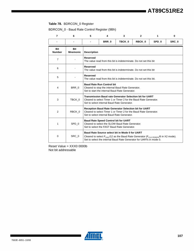
AT89C51RE2
Table 78. BDRCON_0 Register
BDRCON_0 - Baud Rate Control Register (9Bh)
Reset Value = XXX0 0000bNot bit addressable
7 6 5 4 3 2 1 0
- - - BRR_0 TBCK_0 RBCK_0 SPD_0 SRC_0
Bit Number
Bit Mnemonic Description
7 -ReservedThe value read from this bit is indeterminate. Do not set this bit
6 -ReservedThe value read from this bit is indeterminate. Do not set this bit
5 -ReservedThe value read from this bit is indeterminate. Do not set this bit.
4 BRR_0Baud Rate Run Control bitCleared to stop the internal Baud Rate Generator. Set to start the internal Baud Rate Generator.
3 TBCK_0Transmission Baud rate Generator Selection bit for UARTCleared to select Timer 1 or Timer 2 for the Baud Rate Generator. Set to select internal Baud Rate Generator.
2 RBCK_0Reception Baud Rate Generator Selection bit for UARTCleared to select Timer 1 or Timer 2 for the Baud Rate Generator. Set to select internal Baud Rate Generator.
1 SPD_0Baud Rate Speed Control bit for UARTCleared to select the SLOW Baud Rate Generator. Set to select the FAST Baud Rate Generator.
0 SRC_0Baud Rate Source select bit in Mode 0 for UART
Cleared to select FOSC/12 as the Baud Rate Generator (FCLK PERIPH/6 in X2 mode). Set to select the internal Baud Rate Generator for UARTs in mode 0.
1077663E–8051–10/08
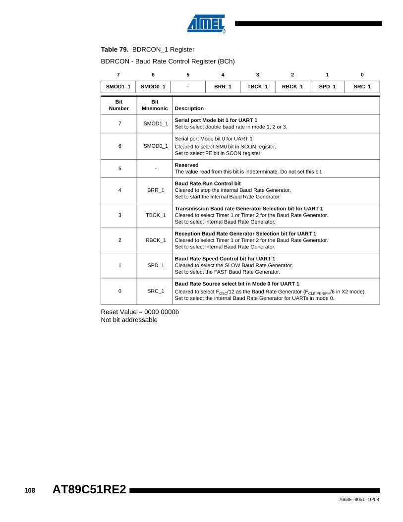
Table 79. BDRCON_1 Register
BDRCON - Baud Rate Control Register (BCh)
Reset Value = 0000 0000bNot bit addressable
7 6 5 4 3 2 1 0
SMOD1_1 SMOD0_1 - BRR_1 TBCK_1 RBCK_1 SPD_1 SRC_1
Bit Number
Bit Mnemonic Description
7 SMOD1_1Serial port Mode bit 1 for UART 1Set to select double baud rate in mode 1, 2 or 3.
6 SMOD0_1Serial port Mode bit 0 for UART 1
Cleared to select SM0 bit in SCON register. Set to select FE bit in SCON register.
5 -ReservedThe value read from this bit is indeterminate. Do not set this bit.
4 BRR_1Baud Rate Run Control bitCleared to stop the internal Baud Rate Generator. Set to start the internal Baud Rate Generator.
3 TBCK_1Transmission Baud rate Generator Selection bit for UART 1Cleared to select Timer 1 or Timer 2 for the Baud Rate Generator. Set to select internal Baud Rate Generator.
2 RBCK_1Reception Baud Rate Generator Selection bit for UART 1Cleared to select Timer 1 or Timer 2 for the Baud Rate Generator. Set to select internal Baud Rate Generator.
1 SPD_1Baud Rate Speed Control bit for UART 1Cleared to select the SLOW Baud Rate Generator. Set to select the FAST Baud Rate Generator.
0 SRC_1Baud Rate Source select bit in Mode 0 for UART 1
Cleared to select FOSC/12 as the Baud Rate Generator (FCLK PERIPH/6 in X2 mode). Set to select the internal Baud Rate Generator for UARTs in mode 0.
1087663E–8051–10/08
AT89C51RE2
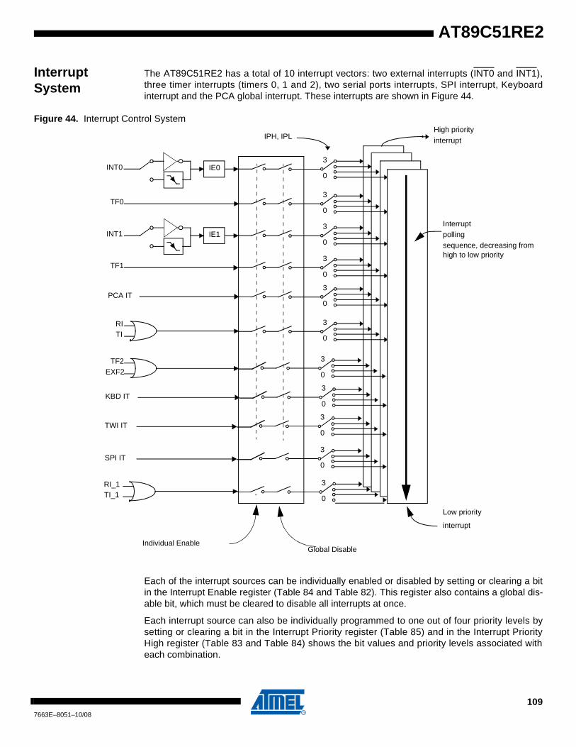
AT89C51RE2
Interrupt System
The AT89C51RE2 has a total of 10 interrupt vectors: two external interrupts (INT0 and INT1),three timer interrupts (timers 0, 1 and 2), two serial ports interrupts, SPI interrupt, Keyboardinterrupt and the PCA global interrupt. These interrupts are shown in Figure 44.
Figure 44. Interrupt Control System
Each of the interrupt sources can be individually enabled or disabled by setting or clearing a bitin the Interrupt Enable register (Table 84 and Table 82). This register also contains a global dis-able bit, which must be cleared to disable all interrupts at once.
Each interrupt source can also be individually programmed to one out of four priority levels bysetting or clearing a bit in the Interrupt Priority register (Table 85) and in the Interrupt PriorityHigh register (Table 83 and Table 84) shows the bit values and priority levels associated witheach combination.
IE1
0
3
High priorityinterrupt
Interruptpollingsequence, decreasing from high to low priority
Low priority
interrupt
Global DisableIndividual Enable
EXF2TF2
TIRI
TF0
INT0
INT1
TF1
IPH, IPL
IE0
0
3
0
3
0
3
0
3
0
3
0
3
PCA IT
KBD IT
SPI IT
0
3
0
3
TI_1RI_1
0
3
TWI IT0
3
1097663E–8051–10/08
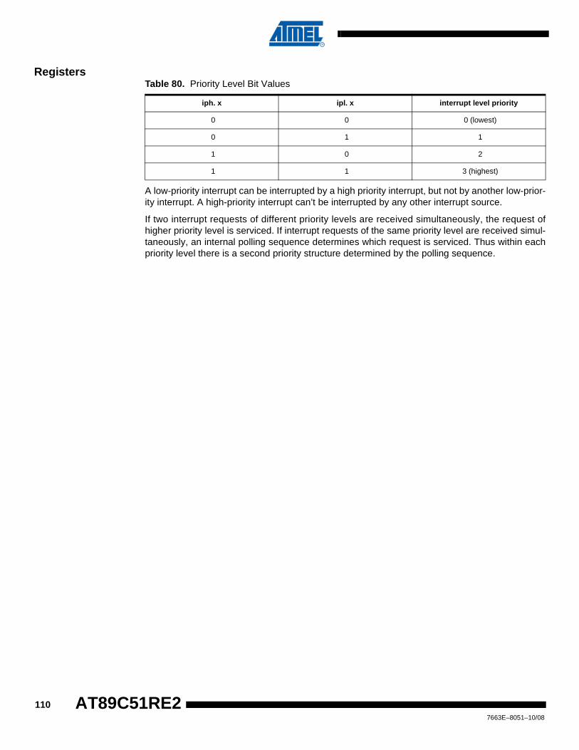
RegistersTable 80. Priority Level Bit Values
A low-priority interrupt can be interrupted by a high priority interrupt, but not by another low-prior-ity interrupt. A high-priority interrupt can’t be interrupted by any other interrupt source.
If two interrupt requests of different priority levels are received simultaneously, the request ofhigher priority level is serviced. If interrupt requests of the same priority level are received simul-taneously, an internal polling sequence determines which request is serviced. Thus within eachpriority level there is a second priority structure determined by the polling sequence.
iph. x ipl. x interrupt level priority
0 0 0 (lowest)
0 1 1
1 0 2
1 1 3 (highest)
1107663E–8051–10/08
AT89C51RE2
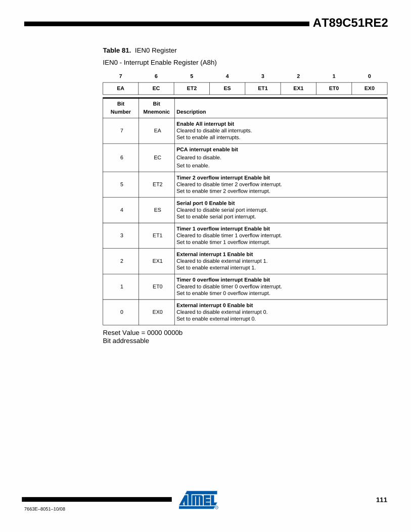
AT89C51RE2
Table 81. IEN0 Register
IEN0 - Interrupt Enable Register (A8h)
Reset Value = 0000 0000bBit addressable
7 6 5 4 3 2 1 0
EA EC ET2 ES ET1 EX1 ET0 EX0
Bit
Number
Bit
Mnemonic Description
7 EAEnable All interrupt bitCleared to disable all interrupts. Set to enable all interrupts.
6 EC
PCA interrupt enable bit
Cleared to disable.
Set to enable.
5 ET2Timer 2 overflow interrupt Enable bitCleared to disable timer 2 overflow interrupt. Set to enable timer 2 overflow interrupt.
4 ESSerial port 0 Enable bitCleared to disable serial port interrupt. Set to enable serial port interrupt.
3 ET1Timer 1 overflow interrupt Enable bitCleared to disable timer 1 overflow interrupt. Set to enable timer 1 overflow interrupt.
2 EX1External interrupt 1 Enable bitCleared to disable external interrupt 1.Set to enable external interrupt 1.
1 ET0Timer 0 overflow interrupt Enable bitCleared to disable timer 0 overflow interrupt. Set to enable timer 0 overflow interrupt.
0 EX0External interrupt 0 Enable bitCleared to disable external interrupt 0.Set to enable external interrupt 0.
1117663E–8051–10/08
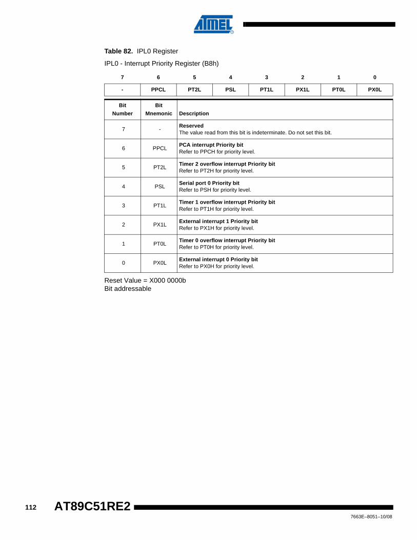
Table 82. IPL0 Register
IPL0 - Interrupt Priority Register (B8h)
Reset Value = X000 0000bBit addressable
7 6 5 4 3 2 1 0
- PPCL PT2L PSL PT1L PX1L PT0L PX0L
Bit
Number
Bit
Mnemonic Description
7 -ReservedThe value read from this bit is indeterminate. Do not set this bit.
6 PPCLPCA interrupt Priority bitRefer to PPCH for priority level.
5 PT2LTimer 2 overflow interrupt Priority bitRefer to PT2H for priority level.
4 PSLSerial port 0 Priority bitRefer to PSH for priority level.
3 PT1LTimer 1 overflow interrupt Priority bitRefer to PT1H for priority level.
2 PX1LExternal interrupt 1 Priority bitRefer to PX1H for priority level.
1 PT0LTimer 0 overflow interrupt Priority bitRefer to PT0H for priority level.
0 PX0LExternal interrupt 0 Priority bitRefer to PX0H for priority level.
1127663E–8051–10/08
AT89C51RE2
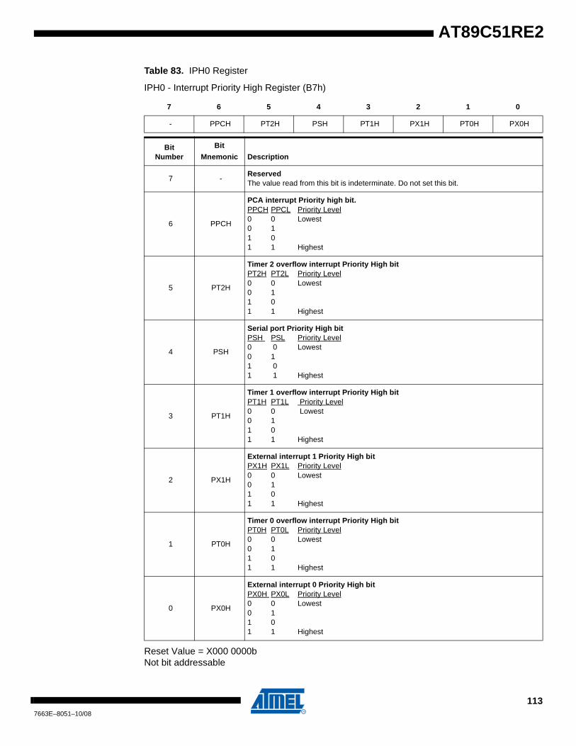
AT89C51RE2
Table 83. IPH0 Register
IPH0 - Interrupt Priority High Register (B7h)
Reset Value = X000 0000bNot bit addressable
7 6 5 4 3 2 1 0
- PPCH PT2H PSH PT1H PX1H PT0H PX0H
Bit Number
Bit
Mnemonic Description
7 -ReservedThe value read from this bit is indeterminate. Do not set this bit.
6 PPCH
PCA interrupt Priority high bit. PPCH PPCL Priority Level0 0 Lowest0 11 01 1 Highest
5 PT2H
Timer 2 overflow interrupt Priority High bitPT2H PT2L Priority Level0 0 Lowest0 11 01 1 Highest
4 PSH
Serial port Priority High bitPSH PSL Priority Level0 0 Lowest0 11 01 1 Highest
3 PT1H
Timer 1 overflow interrupt Priority High bitPT1H PT1L Priority Level0 0 Lowest0 11 01 1 Highest
2 PX1H
External interrupt 1 Priority High bitPX1H PX1L Priority Level0 0 Lowest0 11 01 1 Highest
1 PT0H
Timer 0 overflow interrupt Priority High bitPT0H PT0L Priority Level0 0 Lowest0 11 01 1 Highest
0 PX0H
External interrupt 0 Priority High bitPX0H PX0L Priority Level0 0 Lowest0 11 01 1 Highest
1137663E–8051–10/08
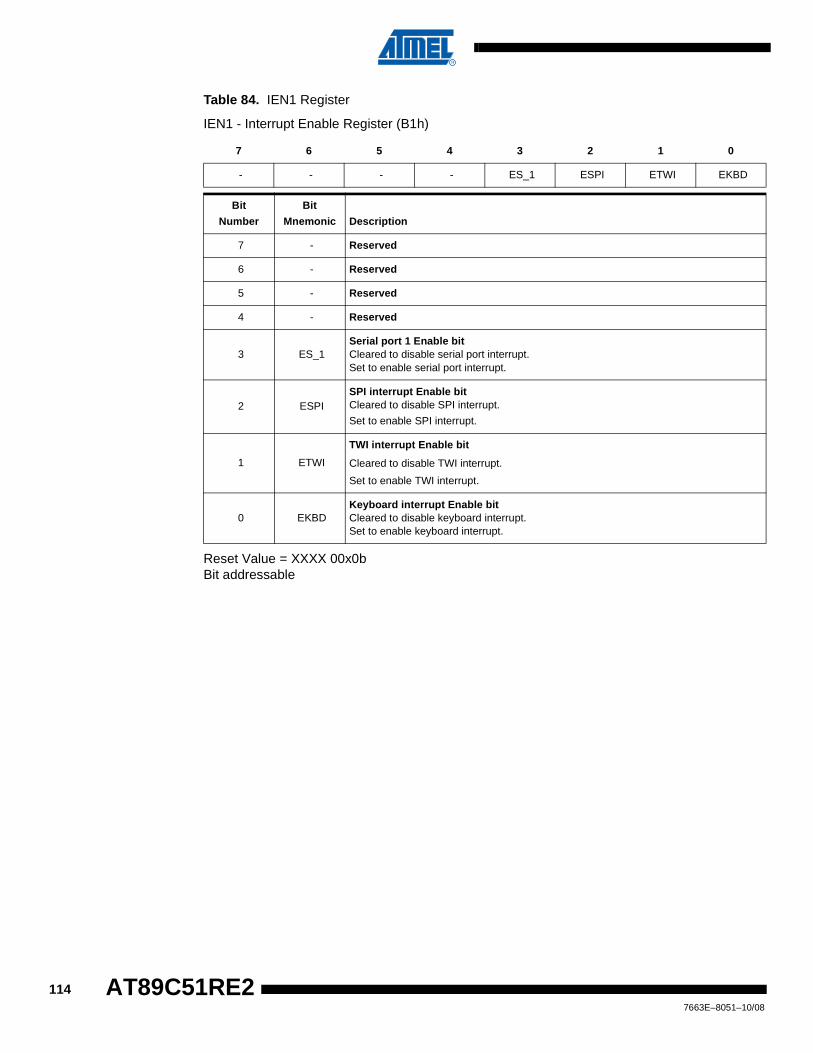
Table 84. IEN1 Register
IEN1 - Interrupt Enable Register (B1h)
Reset Value = XXXX 00x0bBit addressable
7 6 5 4 3 2 1 0
- - - - ES_1 ESPI ETWI EKBD
Bit
Number
Bit
Mnemonic Description
7 - Reserved
6 - Reserved
5 - Reserved
4 - Reserved
3 ES_1Serial port 1 Enable bitCleared to disable serial port interrupt. Set to enable serial port interrupt.
2 ESPISPI interrupt Enable bitCleared to disable SPI interrupt.
Set to enable SPI interrupt.
1 ETWI
TWI interrupt Enable bit
Cleared to disable TWI interrupt.
Set to enable TWI interrupt.
0 EKBDKeyboard interrupt Enable bitCleared to disable keyboard interrupt. Set to enable keyboard interrupt.
1147663E–8051–10/08
AT89C51RE2
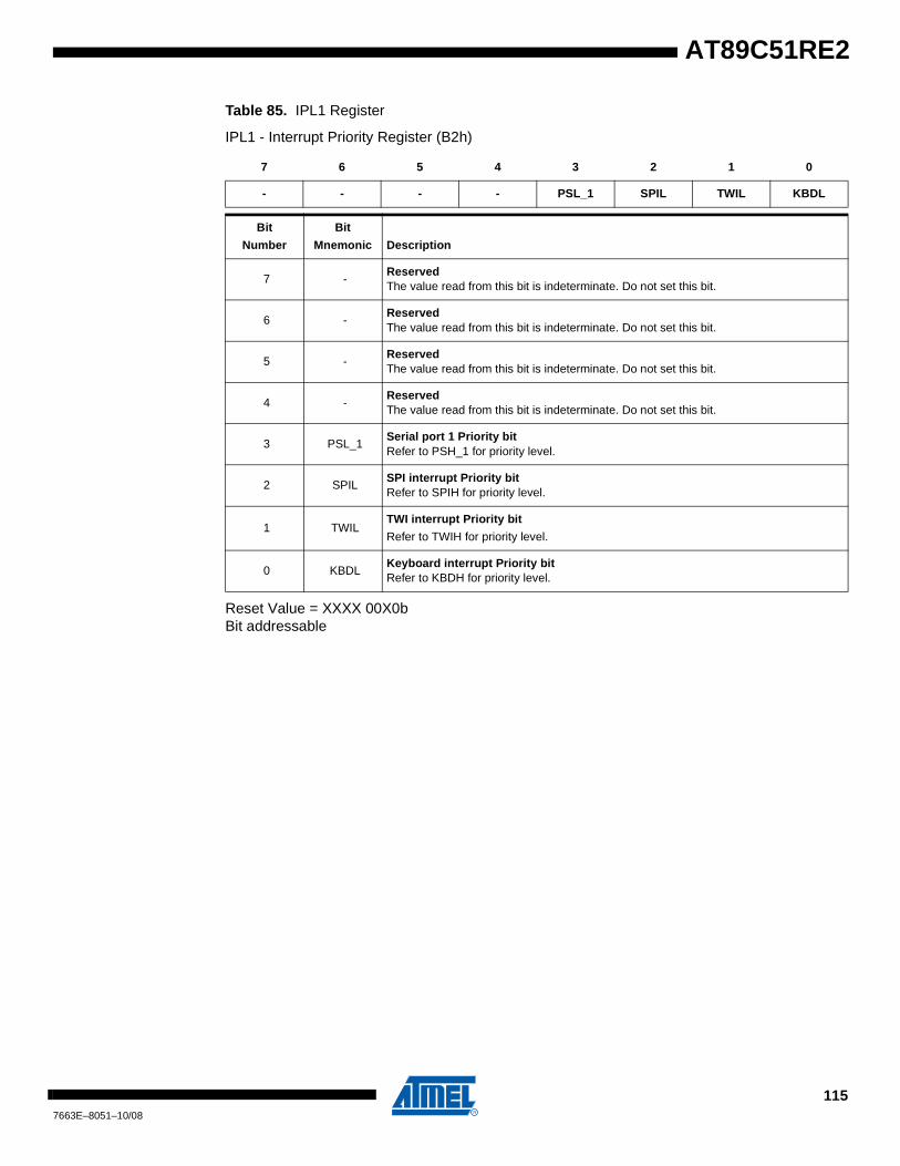
AT89C51RE2
Table 85. IPL1 Register
IPL1 - Interrupt Priority Register (B2h)
Reset Value = XXXX 00X0bBit addressable
7 6 5 4 3 2 1 0
- - - - PSL_1 SPIL TWIL KBDL
Bit
Number
Bit
Mnemonic Description
7 -ReservedThe value read from this bit is indeterminate. Do not set this bit.
6 -ReservedThe value read from this bit is indeterminate. Do not set this bit.
5 -ReservedThe value read from this bit is indeterminate. Do not set this bit.
4 -ReservedThe value read from this bit is indeterminate. Do not set this bit.
3 PSL_1Serial port 1 Priority bitRefer to PSH_1 for priority level.
2 SPILSPI interrupt Priority bitRefer to SPIH for priority level.
1 TWILTWI interrupt Priority bit
Refer to TWIH for priority level.
0 KBDLKeyboard interrupt Priority bitRefer to KBDH for priority level.
1157663E–8051–10/08
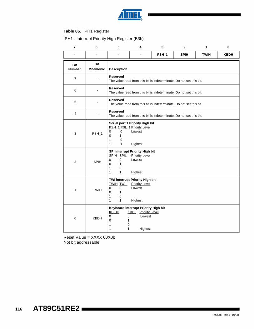
Table 86. IPH1 Register
IPH1 - Interrupt Priority High Register (B3h)
Reset Value = XXXX 00X0bNot bit addressable
7 6 5 4 3 2 1 0
- - - - PSH_1 SPIH TWIH KBDH
Bit Number
Bit
Mnemonic Description
7 -ReservedThe value read from this bit is indeterminate. Do not set this bit.
6 -ReservedThe value read from this bit is indeterminate. Do not set this bit.
5 -ReservedThe value read from this bit is indeterminate. Do not set this bit.
4 -ReservedThe value read from this bit is indeterminate. Do not set this bit.
3 PSH_1
Serial port 1 Priority High bitPSH_1 PSL_1 Priority Level0 0 Lowest0 11 01 1 Highest
2 SPIH
SPI interrupt Priority High bitSPIH SPIL Priority Level0 0 Lowest0 11 01 1 Highest
1 TWIH
TWI interrupt Priority High bitTWIH TWIL Priority Level0 0 Lowest0 11 01 1 Highest
0 KBDH
Keyboard interrupt Priority High bitKB DH KBDL Priority Level0 0 Lowest0 11 01 1 Highest
1167663E–8051–10/08
AT89C51RE2
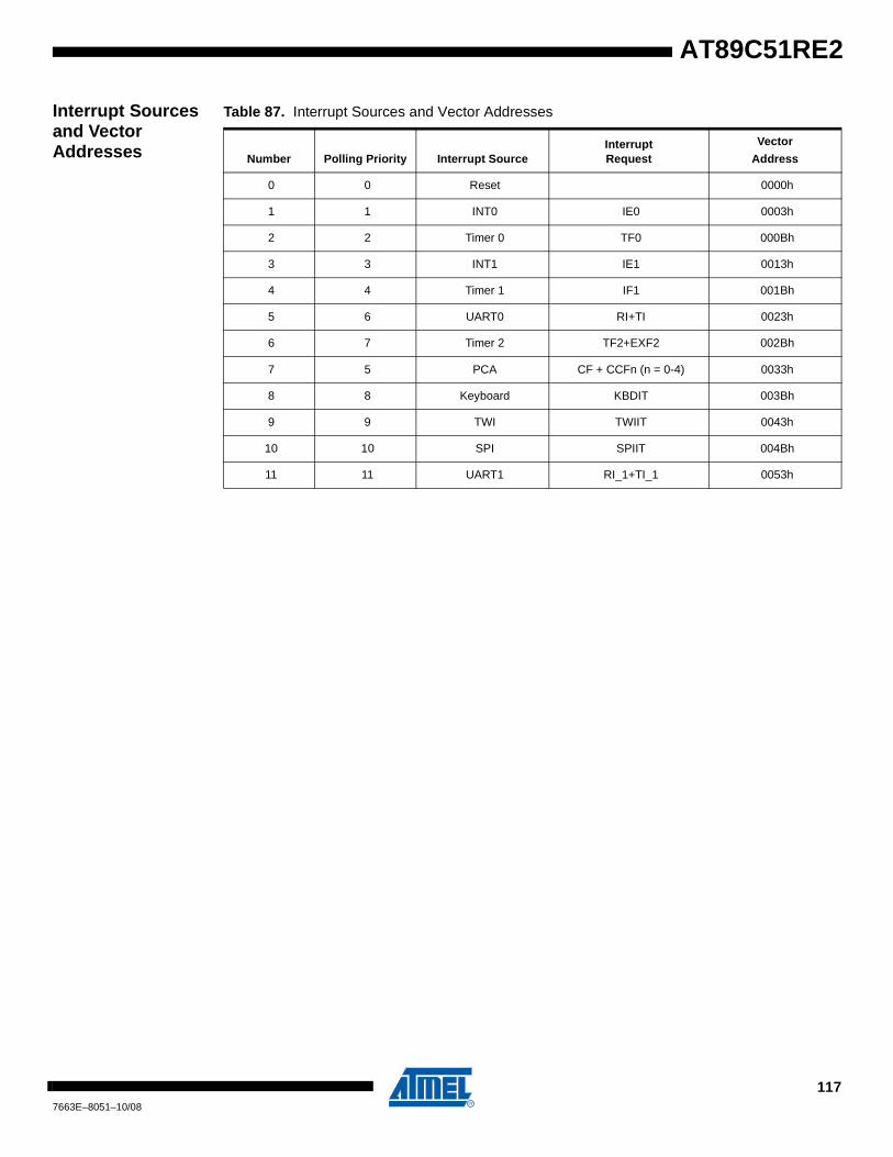
AT89C51RE2
Interrupt Sources and Vector Addresses
Table 87. Interrupt Sources and Vector Addresses
Number Polling Priority Interrupt SourceInterruptRequest
Vector
Address
0 0 Reset 0000h
1 1 INT0 IE0 0003h
2 2 Timer 0 TF0 000Bh
3 3 INT1 IE1 0013h
4 4 Timer 1 IF1 001Bh
5 6 UART0 RI+TI 0023h
6 7 Timer 2 TF2+EXF2 002Bh
7 5 PCA CF + CCFn (n = 0-4) 0033h
8 8 Keyboard KBDIT 003Bh
9 9 TWI TWIIT 0043h
10 10 SPI SPIIT 004Bh
11 11 UART1 RI_1+TI_1 0053h
1177663E–8051–10/08
Power Management
Introduction Two power reduction modes are implemented in the AT89C51RE2. The Idle mode and thePower-Down mode. These modes are detailed in the following sections. In addition to thesepower reduction modes, the clocks of the core and peripherals can be dynamically divided by 2using the X2 mode detailed in Section “Enhanced Features”, page 13.
Idle Mode Idle mode is a power reduction mode that reduces the power consumption. In this mode, pro-gram execution halts. Idle mode freezes the clock to the CPU at known states while theperipherals continue to be clocked. The CPU status before entering Idle mode is preserved, i.e.,the program counter and program status word register retain their data for the duration of Idlemode. The contents of the SFRs and RAM are also retained. The status of the Port pins duringIdle mode is detailed in Table 88.
Entering Idle Mode To enter Idle mode, set the IDL bit in PCON register (see Table 89). The AT89C51RE2 entersIdle mode upon execution of the instruction that sets IDL bit. The instruction that sets IDL bit isthe last instruction executed.
Note: If IDL bit and PD bit are set simultaneously, the AT89C51RE2 enters Power-Down mode. Then itdoes not go in Idle mode when exiting Power-Down mode.
Exiting Idle Mode There are two ways to exit Idle mode:
1. Generate an enabled interrupt.
– Hardware clears IDL bit in PCON register which restores the clock to the CPU. Execution resumes with the interrupt service routine. Upon completion of the interrupt service routine, program execution resumes with the instruction immediately following the instruction that activated Idle mode. The general purpose flags (GF1 and GF0 in PCON register) may be used to indicate whether an interrupt occurred during normal operation or during Idle mode. When Idle mode is exited by an interrupt, the interrupt service routine may examine GF1 and GF0.
2. Generate a reset.
– A logic high on the RST pin clears IDL bit in PCON register directly and asynchronously. This restores the clock to the CPU. Program execution momentarily resumes with the instruction immediately following the instruction that activated the Idle mode and may continue for a number of clock cycles before the internal reset algorithm takes control. Reset initializes the AT89C51RE2 and vectors the CPU to address C:0000h.
Note: During the time that execution resumes, the internal RAM cannot be accessed; however, it is pos-sible for the Port pins to be accessed. To avoid unexpected outputs at the Port pins, the instructionimmediately following the instruction that activated Idle mode should not write to a Port pin or tothe external RAM.
Power-Down Mode The Power-Down mode places the AT89C51RE2 in a very low power state. Power-Down modestops the oscillator, freezes all clock at known states. The CPU status prior to entering Power-Down mode is preserved, i.e., the program counter, program status word register retain theirdata for the duration of Power-Down mode. In addition, the SFR and RAM contents are pre-served. The status of the Port pins during Power-Down mode is detailed in Table 88.Note: VCC may be reduced to as low as VRET during Power-Down mode to further reduce power dissi-
pation. Take care, however, that VDD is not reduced until Power-Down mode is invoked.
1187663E–8051–10/08
AT89C51RE2
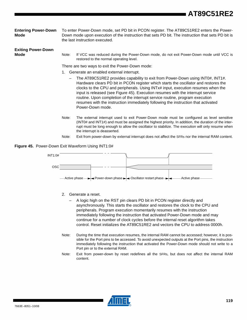
AT89C51RE2
Entering Power-Down Mode
To enter Power-Down mode, set PD bit in PCON register. The AT89C51RE2 enters the Power-Down mode upon execution of the instruction that sets PD bit. The instruction that sets PD bit isthe last instruction executed.
Exiting Power-Down Mode Note: If VCC was reduced during the Power-Down mode, do not exit Power-Down mode until VCC is
restored to the normal operating level.
There are two ways to exit the Power-Down mode:
1. Generate an enabled external interrupt.
– The AT89C51RE2 provides capability to exit from Power-Down using INT0#, INT1#.Hardware clears PD bit in PCON register which starts the oscillator and restores the clocks to the CPU and peripherals. Using INTx# input, execution resumes when the input is released (see Figure 45). Execution resumes with the interrupt service routine. Upon completion of the interrupt service routine, program execution resumes with the instruction immediately following the instruction that activated Power-Down mode.
Note: The external interrupt used to exit Power-Down mode must be configured as level sensitive(INT0# and INT1#) and must be assigned the highest priority. In addition, the duration of the inter-rupt must be long enough to allow the oscillator to stabilize. The execution will only resume whenthe interrupt is deasserted.
Note: Exit from power-down by external interrupt does not affect the SFRs nor the internal RAM content.
Figure 45. Power-Down Exit Waveform Using INT1:0#
2. Generate a reset.
– A logic high on the RST pin clears PD bit in PCON register directly and asynchronously. This starts the oscillator and restores the clock to the CPU and peripherals. Program execution momentarily resumes with the instruction immediately following the instruction that activated Power-Down mode and may continue for a number of clock cycles before the internal reset algorithm takes control. Reset initializes the AT89C51RE2 and vectors the CPU to address 0000h.
Note: During the time that execution resumes, the internal RAM cannot be accessed; however, it is pos-sible for the Port pins to be accessed. To avoid unexpected outputs at the Port pins, the instructionimmediately following the instruction that activated the Power-Down mode should not write to aPort pin or to the external RAM.
Note: Exit from power-down by reset redefines all the SFRs, but does not affect the internal RAMcontent.
INT1:0#
OSC
Power-down phase Oscillator restart phase Active phaseActive phase
1197663E–8051–10/08
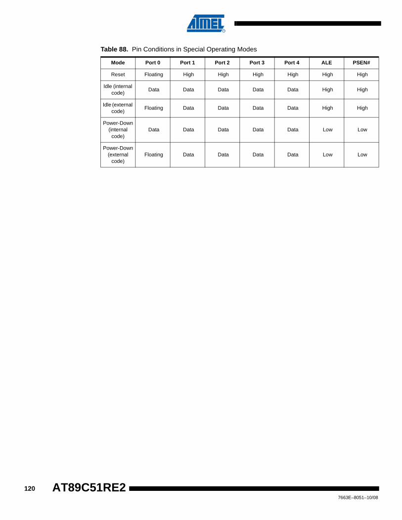
Table 88. Pin Conditions in Special Operating Modes
Mode Port 0 Port 1 Port 2 Port 3 Port 4 ALE PSEN#
Reset Floating High High High High High High
Idle (internal code)
Data Data Data Data Data High High
Idle (external code)
Floating Data Data Data Data High High
Power-Down (internal code)
Data Data Data Data Data Low Low
Power-Down (external
code)Floating Data Data Data Data Low Low
1207663E–8051–10/08
AT89C51RE2
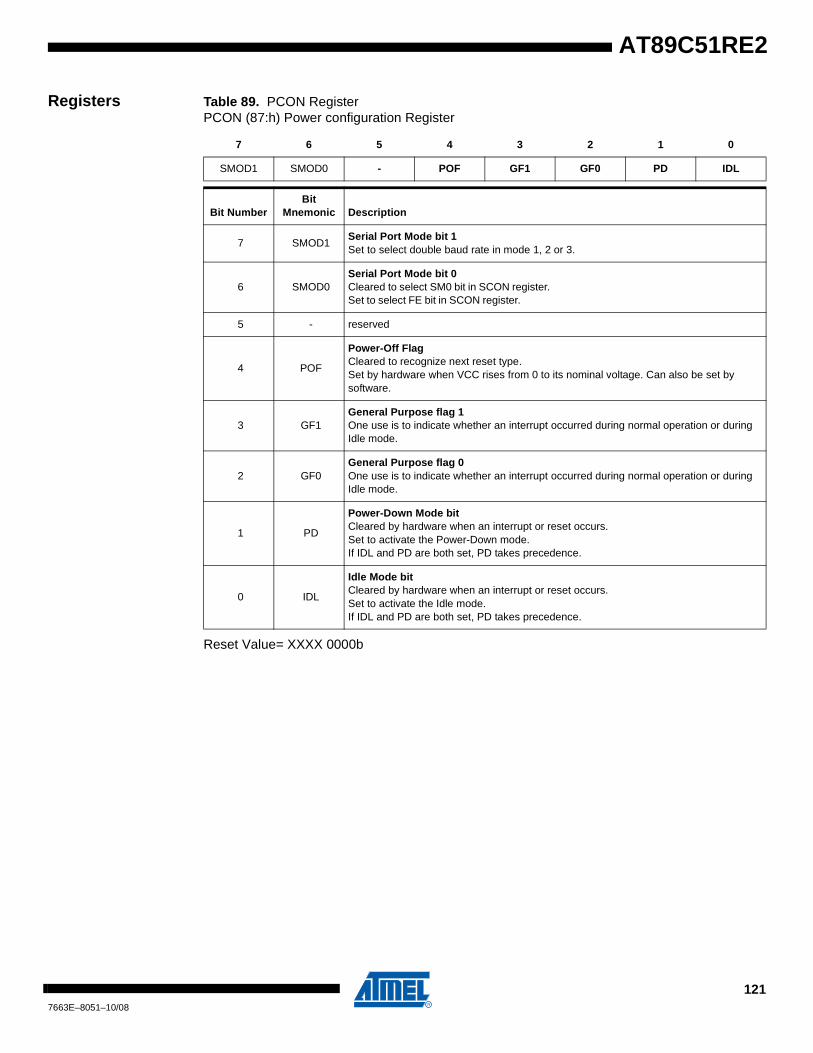
AT89C51RE2
Registers Table 89. PCON RegisterPCON (87:h) Power configuration Register
Reset Value= XXXX 0000b
7 6 5 4 3 2 1 0
SMOD1 SMOD0 - POF GF1 GF0 PD IDL
Bit NumberBit
Mnemonic Description
7 SMOD1Serial Port Mode bit 1Set to select double baud rate in mode 1, 2 or 3.
6 SMOD0Serial Port Mode bit 0Cleared to select SM0 bit in SCON register. Set to select FE bit in SCON register.
5 - reserved
4 POF
Power-Off FlagCleared to recognize next reset type.Set by hardware when VCC rises from 0 to its nominal voltage. Can also be set by software.
3 GF1General Purpose flag 1One use is to indicate whether an interrupt occurred during normal operation or during Idle mode.
2 GF0General Purpose flag 0One use is to indicate whether an interrupt occurred during normal operation or during Idle mode.
1 PD
Power-Down Mode bitCleared by hardware when an interrupt or reset occurs.Set to activate the Power-Down mode.If IDL and PD are both set, PD takes precedence.
0 IDL
Idle Mode bitCleared by hardware when an interrupt or reset occurs.Set to activate the Idle mode.If IDL and PD are both set, PD takes precedence.
1217663E–8051–10/08
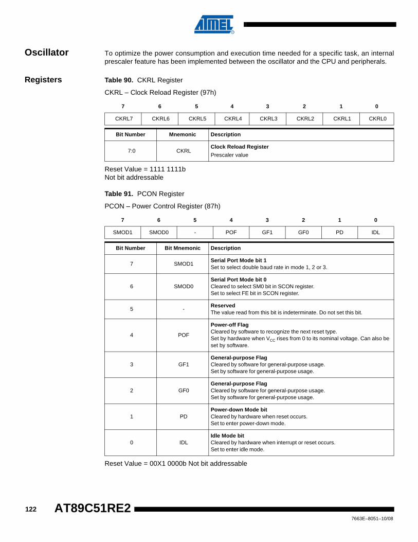
Oscillator To optimize the power consumption and execution time needed for a specific task, an internalprescaler feature has been implemented between the oscillator and the CPU and peripherals.
Registers Table 90. CKRL Register
CKRL – Clock Reload Register (97h)
Reset Value = 1111 1111bNot bit addressable
Table 91. PCON Register
PCON – Power Control Register (87h)
Reset Value = 00X1 0000b Not bit addressable
7 6 5 4 3 2 1 0
CKRL7 CKRL6 CKRL5 CKRL4 CKRL3 CKRL2 CKRL1 CKRL0
Bit Number Mnemonic Description
7:0 CKRLClock Reload Register
Prescaler value
7 6 5 4 3 2 1 0
SMOD1 SMOD0 - POF GF1 GF0 PD IDL
Bit Number Bit Mnemonic Description
7 SMOD1Serial Port Mode bit 1Set to select double baud rate in mode 1, 2 or 3.
6 SMOD0Serial Port Mode bit 0Cleared to select SM0 bit in SCON register. Set to select FE bit in SCON register.
5 -ReservedThe value read from this bit is indeterminate. Do not set this bit.
4 POF
Power-off FlagCleared by software to recognize the next reset type. Set by hardware when VCC rises from 0 to its nominal voltage. Can also be set by software.
3 GF1General-purpose FlagCleared by software for general-purpose usage. Set by software for general-purpose usage.
2 GF0General-purpose FlagCleared by software for general-purpose usage. Set by software for general-purpose usage.
1 PDPower-down Mode bitCleared by hardware when reset occurs. Set to enter power-down mode.
0 IDLIdle Mode bitCleared by hardware when interrupt or reset occurs. Set to enter idle mode.
1227663E–8051–10/08
AT89C51RE2
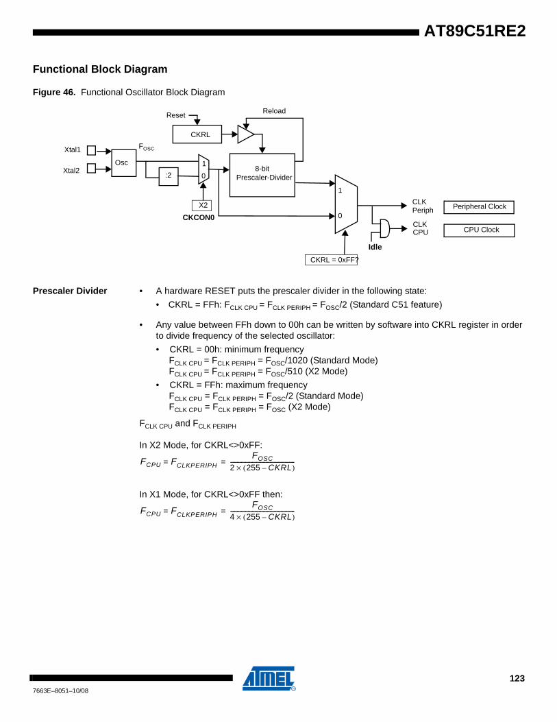
AT89C51RE2
Functional Block Diagram
Figure 46. Functional Oscillator Block Diagram
Prescaler Divider • A hardware RESET puts the prescaler divider in the following state:
• CKRL = FFh: FCLK CPU = FCLK PERIPH = FOSC/2 (Standard C51 feature)
• Any value between FFh down to 00h can be written by software into CKRL register in order to divide frequency of the selected oscillator:
• CKRL = 00h: minimum frequency FCLK CPU = FCLK PERIPH = FOSC/1020 (Standard Mode)FCLK CPU = FCLK PERIPH = FOSC/510 (X2 Mode)
• CKRL = FFh: maximum frequencyFCLK CPU = FCLK PERIPH = FOSC/2 (Standard Mode) FCLK CPU = FCLK PERIPH = FOSC (X2 Mode)
FCLK CPU and FCLK PERIPH
In X2 Mode, for CKRL<>0xFF:
In X1 Mode, for CKRL<>0xFF then:
Xtal2
Xtal1
Osc
CLK
Idle
CPU Clock
CKRL
Reload
8-bitPrescaler-Divider
Reset
Peripheral Clock
:2
X2
0
1
FOSC
CKCON0
CLKPeriph
CPU
CKRL = 0xFF?
0
1
FCPU F= CLKPERIPH
FOSC
2 255 CKRL–( )×-----------------------------------------------=
FCPU F= CLKPERIPH
FOSC
4 255 CKRL–( )×-----------------------------------------------=
1237663E–8051–10/08

Hardware Watchdog Timer
The WDT is intended as a recovery method in situations where the CPU may be subjected tosoftware upset. The WDT consists of a 14-bit counter and the WatchDog Timer ReSeT(WDTRST) SFR. The WDT is by default disabled from exiting reset. To enable the WDT, usermust write 01EH and 0E1H in sequence to the WDTRST, SFR location 0A6H. When WDT isenabled, it will increment every machine cycle while the oscillator is running and there is no wayto disable the WDT except through reset (either hardware reset or WDT overflow reset). WhenWDT overflows, it will drive an output RESET HIGH pulse at the RST-pin.
Using the WDT To enable the WDT, user must write 01EH and 0E1H in sequence to the WDTRST, SFR loca-tion 0A6H. When WDT is enabled, the user needs to service it by writing to 01EH and 0E1H toWDTRST to avoid WDT overflow. The 14-bit counter overflows when it reaches 16383 (3FFFH)and this will reset the device. When WDT is enabled, it will increment every machine cycle whilethe oscillator is running. This means the user must reset the WDT at least every 16383 machinecycle. To reset the WDT the user must write 01EH and 0E1H to WDTRST. WDTRST is a writeonly register. The WDT counter cannot be read or written. When WDT overflows, it will generatean output RESET pulse at the RST-pin. The RESET pulse duration is 96 x TCLK PERIPH, whereTCLK PERIPH= 1/FCLK PERIPH. To make the best use of the WDT, it should be serviced in those sec-tions of code that will periodically be executed within the time required to prevent a WDT reset.
To have a more powerful WDT, a 27 counter has been added to extend the Time-out capability,ranking from 16ms to 2s @ FOSCA = 12MHz. To manage this feature, refer to WDTPRG registerdescription, Table 92.
Table 92. WDTRST Register
WDTRST - Watchdog Reset Register (0A6h)
Reset Value = XXXX XXXXb
Write only, this SFR is used to reset/enable the WDT by writing 01EH then 0E1H in sequence.
7 6 5 4 3 2 1 0
- - - - - - - -
1247663E–8051–10/08
AT89C51RE2
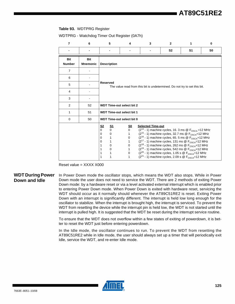
AT89C51RE2
Table 93. WDTPRG Register
WDTPRG - Watchdog Timer Out Register (0A7h)
Reset value = XXXX X000
WDT During Power Down and Idle
In Power Down mode the oscillator stops, which means the WDT also stops. While in PowerDown mode the user does not need to service the WDT. There are 2 methods of exiting PowerDown mode: by a hardware reset or via a level activated external interrupt which is enabled priorto entering Power Down mode. When Power Down is exited with hardware reset, servicing theWDT should occur as it normally should whenever the AT89C51RE2 is reset. Exiting PowerDown with an interrupt is significantly different. The interrupt is held low long enough for theoscillator to stabilize. When the interrupt is brought high, the interrupt is serviced. To prevent theWDT from resetting the device while the interrupt pin is held low, the WDT is not started until theinterrupt is pulled high. It is suggested that the WDT be reset during the interrupt service routine.
To ensure that the WDT does not overflow within a few states of exiting of powerdown, it is bet-ter to reset the WDT just before entering powerdown.
In the Idle mode, the oscillator continues to run. To prevent the WDT from resetting theAT89C51RE2 while in Idle mode, the user should always set up a timer that will periodically exitIdle, service the WDT, and re-enter Idle mode.
7 6 5 4 3 2 1 0
- - - - - S2 S1 S0
Bit
Number
Bit
Mnemonic Description
7 -
ReservedThe value read from this bit is undetermined. Do not try to set this bit.
6 -
5 -
4 -
3 -
2 S2 WDT Time-out select bit 2
1 S1 WDT Time-out select bit 1
0 S0 WDT Time-out select bit 0
S2 S1 S0 Selected Time-out0 0 0 (214 - 1) machine cycles, 16. 3 ms @ FOSCA =12 MHz0 0 1 (215 - 1) machine cycles, 32.7 ms @ FOSCA=12 MHz0 1 0 (216 - 1) machine cycles, 65. 5 ms @ FOSCA=12 MHz0 1 1 (217 - 1) machine cycles, 131 ms @ FOSCA=12 MHz1 0 0 (218 - 1) machine cycles, 262 ms @ FOSCA=12 MHz1 0 1 (219 - 1) machine cycles, 542 ms @ FOSCA=12 MHz1 1 0 (220 - 1) machine cycles, 1.05 s @ FOSCA=12 MHz1 1 1 (221 - 1) machine cycles, 2.09 s @ FOSCA=12 MHz
1257663E–8051–10/08
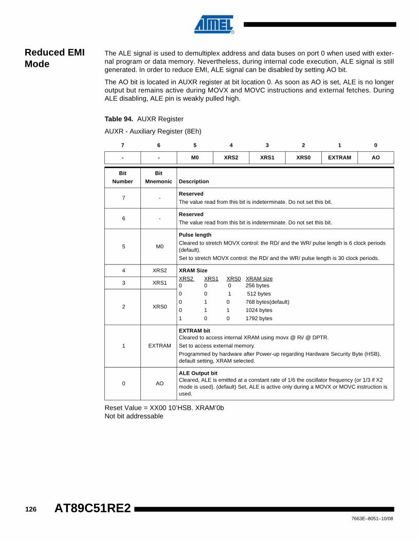
1267663E–8051–10/08
AT89C51RE2
Reduced EMI Mode
The ALE signal is used to demultiplex address and data buses on port 0 when used with exter-nal program or data memory. Nevertheless, during internal code execution, ALE signal is stillgenerated. In order to reduce EMI, ALE signal can be disabled by setting AO bit.
The AO bit is located in AUXR register at bit location 0. As soon as AO is set, ALE is no longeroutput but remains active during MOVX and MOVC instructions and external fetches. DuringALE disabling, ALE pin is weakly pulled high.
Table 94. AUXR Register
AUXR - Auxiliary Register (8Eh)
Reset Value = XX00 10’HSB. XRAM’0bNot bit addressable
7 6 5 4 3 2 1 0
- - M0 XRS2 XRS1 XRS0 EXTRAM AO
Bit
Number
Bit
Mnemonic Description
7 -Reserved
The value read from this bit is indeterminate. Do not set this bit.
6 -Reserved
The value read from this bit is indeterminate. Do not set this bit.
5 M0
Pulse length
Cleared to stretch MOVX control: the RD/ and the WR/ pulse length is 6 clock periods (default).
Set to stretch MOVX control: the RD/ and the WR/ pulse length is 30 clock periods.
4 XRS2 XRAM Size
XRS2 XRS1 XRS0 XRAM size0 0 0 256 bytes
0 0 1 512 bytes
0 1 0 768 bytes(default)
0 1 1 1024 bytes
1 0 0 1792 bytes
3 XRS1
2 XRS0
1 EXTRAM
EXTRAM bitCleared to access internal XRAM using movx @ Ri/ @ DPTR.
Set to access external memory.
Programmed by hardware after Power-up regarding Hardware Security Byte (HSB), default setting, XRAM selected.
0 AO
ALE Output bitCleared, ALE is emitted at a constant rate of 1/6 the oscillator frequency (or 1/3 if X2 mode is used). (default) Set, ALE is active only during a MOVX or MOVC instruction is used.
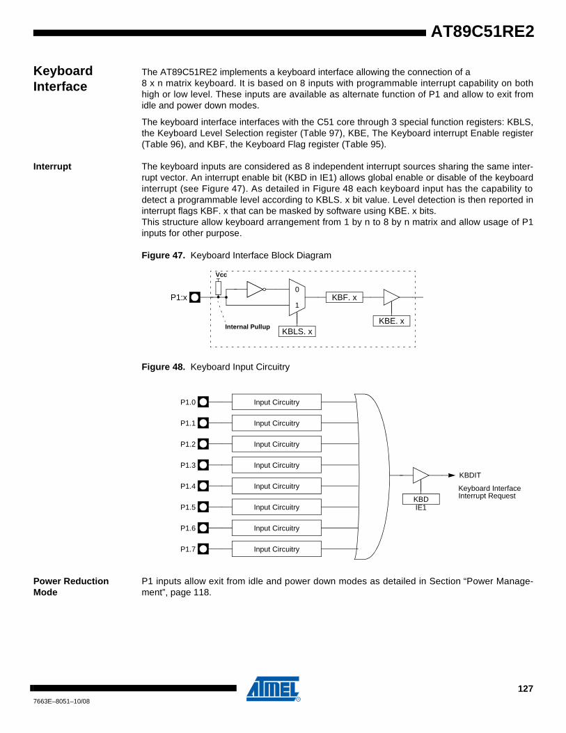
AT89C51RE2
Keyboard Interface
The AT89C51RE2 implements a keyboard interface allowing the connection of a 8 x n matrix keyboard. It is based on 8 inputs with programmable interrupt capability on bothhigh or low level. These inputs are available as alternate function of P1 and allow to exit fromidle and power down modes.
The keyboard interface interfaces with the C51 core through 3 special function registers: KBLS,the Keyboard Level Selection register (Table 97), KBE, The Keyboard interrupt Enable register(Table 96), and KBF, the Keyboard Flag register (Table 95).
Interrupt The keyboard inputs are considered as 8 independent interrupt sources sharing the same inter-rupt vector. An interrupt enable bit (KBD in IE1) allows global enable or disable of the keyboardinterrupt (see Figure 47). As detailed in Figure 48 each keyboard input has the capability todetect a programmable level according to KBLS. x bit value. Level detection is then reported ininterrupt flags KBF. x that can be masked by software using KBE. x bits. This structure allow keyboard arrangement from 1 by n to 8 by n matrix and allow usage of P1inputs for other purpose.
Figure 47. Keyboard Interface Block Diagram
Figure 48. Keyboard Input Circuitry
Power Reduction Mode
P1 inputs allow exit from idle and power down modes as detailed in Section “Power Manage-ment”, page 118.
P1:x
KBE. x
KBF. x
KBLS. x
0
1
Vcc
Internal Pullup
P1.0
Keyboard InterfaceInterrupt RequestKBD
IE1
Input Circuitry
P1.1 Input Circuitry
P1.2 Input Circuitry
P1.3 Input Circuitry
P1.4 Input Circuitry
P1.5 Input Circuitry
P1.6 Input Circuitry
P1.7 Input Circuitry
KBDIT
1277663E–8051–10/08
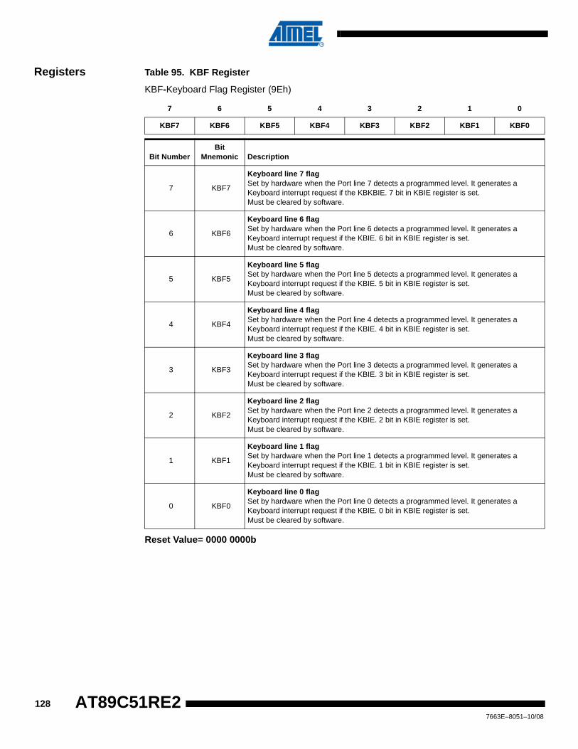
Registers Table 95. KBF Register
KBF-Keyboard Flag Register (9Eh)
Reset Value= 0000 0000b
7 6 5 4 3 2 1 0
KBF7 KBF6 KBF5 KBF4 KBF3 KBF2 KBF1 KBF0
Bit NumberBit
Mnemonic Description
7 KBF7
Keyboard line 7 flagSet by hardware when the Port line 7 detects a programmed level. It generates a Keyboard interrupt request if the KBKBIE. 7 bit in KBIE register is set. Must be cleared by software.
6 KBF6
Keyboard line 6 flag Set by hardware when the Port line 6 detects a programmed level. It generates a Keyboard interrupt request if the KBIE. 6 bit in KBIE register is set. Must be cleared by software.
5 KBF5
Keyboard line 5 flag Set by hardware when the Port line 5 detects a programmed level. It generates a Keyboard interrupt request if the KBIE. 5 bit in KBIE register is set. Must be cleared by software.
4 KBF4
Keyboard line 4 flag Set by hardware when the Port line 4 detects a programmed level. It generates a Keyboard interrupt request if the KBIE. 4 bit in KBIE register is set. Must be cleared by software.
3 KBF3
Keyboard line 3 flagSet by hardware when the Port line 3 detects a programmed level. It generates a Keyboard interrupt request if the KBIE. 3 bit in KBIE register is set. Must be cleared by software.
2 KBF2
Keyboard line 2 flagSet by hardware when the Port line 2 detects a programmed level. It generates a Keyboard interrupt request if the KBIE. 2 bit in KBIE register is set. Must be cleared by software.
1 KBF1
Keyboard line 1 flag Set by hardware when the Port line 1 detects a programmed level. It generates a Keyboard interrupt request if the KBIE. 1 bit in KBIE register is set. Must be cleared by software.
0 KBF0
Keyboard line 0 flag Set by hardware when the Port line 0 detects a programmed level. It generates a Keyboard interrupt request if the KBIE. 0 bit in KBIE register is set. Must be cleared by software.
1287663E–8051–10/08
AT89C51RE2
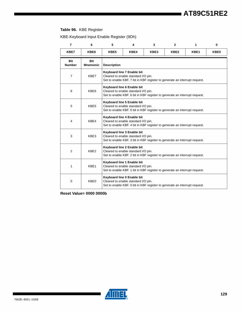
AT89C51RE2
Table 96. KBE Register
KBE-Keyboard Input Enable Register (9Dh)
Reset Value= 0000 0000b
7 6 5 4 3 2 1 0
KBE7 KBE6 KBE5 KBE4 KBE3 KBE2 KBE1 KBE0
BitNumber
BitMnemonic Description
7 KBE7Keyboard line 7 Enable bitCleared to enable standard I/O pin. Set to enable KBF. 7 bit in KBF register to generate an interrupt request.
6 KBE6Keyboard line 6 Enable bitCleared to enable standard I/O pin. Set to enable KBF. 6 bit in KBF register to generate an interrupt request.
5 KBE5Keyboard line 5 Enable bitCleared to enable standard I/O pin. Set to enable KBF. 5 bit in KBF register to generate an interrupt request.
4 KBE4Keyboard line 4 Enable bitCleared to enable standard I/O pin. Set to enable KBF. 4 bit in KBF register to generate an interrupt request.
3 KBE3Keyboard line 3 Enable bitCleared to enable standard I/O pin. Set to enable KBF. 3 bit in KBF register to generate an interrupt request.
2 KBE2Keyboard line 2 Enable bitCleared to enable standard I/O pin. Set to enable KBF. 2 bit in KBF register to generate an interrupt request.
1 KBE1Keyboard line 1 Enable bitCleared to enable standard I/O pin. Set to enable KBF. 1 bit in KBF register to generate an interrupt request.
0 KBE0Keyboard line 0 Enable bitCleared to enable standard I/O pin. Set to enable KBF. 0 bit in KBF register to generate an interrupt request.
1297663E–8051–10/08

Table 97. KBLS Register
KBLS-Keyboard Level Selector Register (9Ch)
Reset Value= 0000 0000b
7 6 5 4 3 2 1 0
KBLS7 KBLS6 KBLS5 KBLS4 KBLS3 KBLS2 KBLS1 KBLS0
Bit NumberBit
Mnemonic Description
7 KBLS7Keyboard line 7 Level Selection bitCleared to enable a low level detection on Port line 7. Set to enable a high level detection on Port line 7.
6 KBLS6Keyboard line 6 Level Selection bitCleared to enable a low level detection on Port line 6. Set to enable a high level detection on Port line 6.
5 KBLS5Keyboard line 5 Level Selection bitCleared to enable a low level detection on Port line 5. Set to enable a high level detection on Port line 5.
4 KBLS4Keyboard line 4 Level Selection bitCleared to enable a low level detection on Port line 4. Set to enable a high level detection on Port line 4.
3 KBLS3Keyboard line 3 Level Selection bitCleared to enable a low level detection on Port line 3.Set to enable a high level detection on Port line 3.
2 KBLS2Keyboard line 2 Level Selection bitCleared to enable a low level detection on Port line 2.Set to enable a high level detection on Port line 2.
1 KBLS1Keyboard line 1 Level Selection bitCleared to enable a low level detection on Port line 1.Set to enable a high level detection on Port line 1.
0 KBLS0Keyboard line 0 Level Selection bitCleared to enable a low level detection on Port line 0.Set to enable a high level detection on Port line 0.
1307663E–8051–10/08
AT89C51RE2

AT89C51RE2
2-wire Interface (TWI) This section describes the 2-wire interface. The 2-wire bus is a bi-directional 2-wireserial communication standard. It is designed primarily for simple but efficient integratedcircuit (IC) control. The system is comprised of two lines, SCL (Serial Clock) and SDA(Serial Data) that carry information between the ICs connected to them. The serial datatransfer is limited to 400 Kbit/s in standard mode. Various communication configurationcan be designed using this bus. Figure 49 shows a typical 2-wire bus configuration. Allthe devices connected to the bus can be master and slave.
Figure 49. 2-wire Bus Configuration
SCL
SDA
device2device1 deviceNdevice3 ...
1317663D–8051–10/08
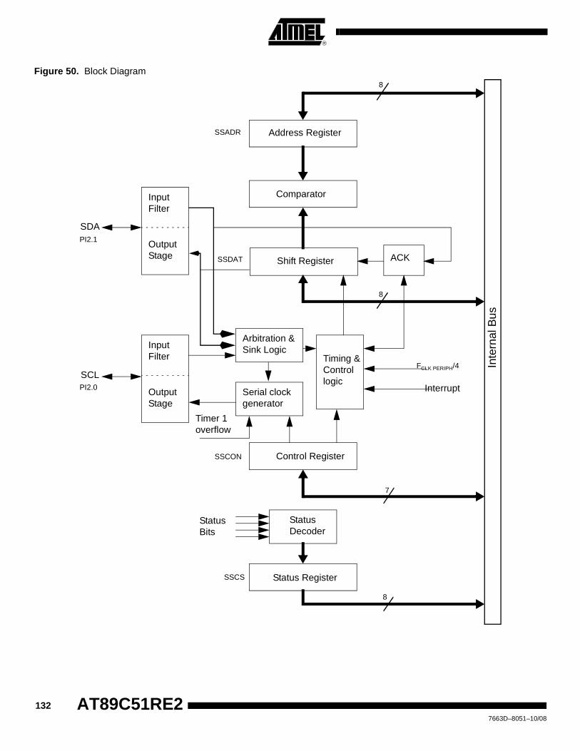
Figure 50. Block Diagram
Address Register
Comparator
Timing & Control logic
Arbitration &Sink Logic
Serial clock generator
Shift Register
Control Register
Status Register
StatusDecoder
InputFilter
OutputStage
InputFilter
OutputStage
ACK
StatusBits
8
8
7
8
Inte
rnal
Bus
Timer 1overflow
FCLK PERIPH/4
Interrupt
SDA
SCL
SSADR
SSCON
SSDAT
SSCS
PI2.1
PI2.0
132 AT89C51RE27663D–8051–10/08

AT89C51RE2
Description The CPU interfaces to the 2-wire logic via the following four 8-bit special function regis-ters: the Synchronous Serial Control register (SSCON; Table 107), the SynchronousSerial Data register (SSDAT; Table 108), the Synchronous Serial Control and Statusregister (SSCS; Table 109) and the Synchronous Serial Address register (SSADR Table112).
SSCON is used to enable the TWI interface, to program the bit rate (see Table 100), toenable slave modes, to acknowledge or not a received data, to send a START or aSTOP condition on the 2-wire bus, and to acknowledge a serial interrupt. A hardwarereset disables the TWI module.
SSCS contains a status code which reflects the status of the 2-wire logic and the 2-wirebus. The three least significant bits are always zero. The five most significant bits con-tains the status code. There are 26 possible status codes. When SSCS contains F8h,no relevant state information is available and no serial interrupt is requested. A valid sta-tus code is available in SSCS one machine cycle after SI is set by hardware and is stillpresent one machine cycle after SI has been reset by software. to Table 106. give thestatus for the master modes and miscellaneous states.
SSDAT contains a byte of serial data to be transmitted or a byte which has just beenreceived. It is addressable while it is not in process of shifting a byte. This occurs when2-wire logic is in a defined state and the serial interrupt flag is set. Data in SSDATremains stable as long as SI is set. While data is being shifted out, data on the bus issimultaneously shifted in; SSDAT always contains the last byte present on the bus.
SSADR may be loaded with the 7-bit slave address (7 most significant bits) to which theTWI module will respond when programmed as a slave transmitter or receiver. The LSBis used to enable general call address (00h) recognition.
Figure 51 shows how a data transfer is accomplished on the 2-wire bus.
Figure 51. Complete Data Transfer on 2-wire Bus
The four operating modes are:
• Master Transmitter
• Master Receiver
• Slave transmitter
• Slave receiver
Data transfer in each mode of operation is shown in Table to Table 106 and Figure 52.to Figure 55.. These figures contain the following abbreviations:
S : START condition
R : Read bit (high level at SDA)
SDA
SCL
Sstartcondition
MSB
1 2 7 8 9ACK
acknowledgementsignal from receiver
acknowledgementsignal from receiver
1 2 3-8 9ACK
stopcondition
Pclock line held lowwhile interrupts are serviced
1337663D–8051–10/08
W: Write bit (low level at SDA)
A: Acknowledge bit (low level at SDA)
A: Not acknowledge bit (high level at SDA)
Data: 8-bit data byte
P : STOP condition
In Figure 52 to Figure 55, circles are used to indicate when the serial interrupt flag is set.The numbers in the circles show the status code held in SSCS. At these points, a ser-vice routine must be executed to continue or complete the serial transfer. These serviceroutines are not critical since the serial transfer is suspended until the serial interruptflag is cleared by software.
When the serial interrupt routine is entered, the status code in SSCS is used to branchto the appropriate service routine. For each status code, the required software actionand details of the following serial transfer are given in Table to Table 106.
Master Transmitter Mode In the master transmitter mode, a number of data bytes are transmitted to a slavereceiver (Figure 52). Before the master transmitter mode can be entered, SSCON mustbe initialised as follows:
CR0, CR1 and CR2 define the internal serial bit rate if external bit rate generator is notused. SSIE must be set to enable TWI. STA, STO and SI must be cleared.
The master transmitter mode may now be entered by setting the STA bit. The 2-wirelogic will now test the 2-wire bus and generate a START condition as soon as the busbecomes free. When a START condition is transmitted, the serial interrupt flag (SI bit inSSCON) is set, and the status code in SSCS will be 08h. This status must be used tovector to an interrupt routine that loads SSDAT with the slave address and the datadirection bit (SLA+W).
When the slave address and the direction bit have been transmitted and an acknowl-edgement bit has been received, SI is set again and a number of status code in SSCSare possible. There are 18h, 20h or 38h for the master mode and also 68h, 78h or B0h ifthe slave mode was enabled (AA=logic 1). The appropriate action to be taken for eachof these status code is detailed in Table . This scheme is repeated until a STOP condi-tion is transmitted.
SSIE, CR2, CR1 and CR0 are not affected by the serial transfer and are referred toTable 7 to Table 11. After a repeated START condition (state 10h) the TWI module mayswitch to the master receiver mode by loading SSDAT with SLA+R.
Master Receiver Mode In the master receiver mode, a number of data bytes are received from a slave transmit-ter (Figure 53). The transfer is initialized as in the master transmitter mode. When theSTART condition has been transmitted, the interrupt routine must load SSDAT with the7-bit slave address and the data direction bit (SLA+R). The serial interrupt flag SI mustthen be cleared before the serial transfer can continue.
Table 98. SSCON Initialization
CR2 SSIE STA STO SI AA CR1 CR0
bit rate 1 0 0 0 X bit rate bit rate
134 AT89C51RE27663D–8051–10/08
AT89C51RE2
When the slave address and the direction bit have been transmitted and an acknowl-edgement bit has been received, the serial interrupt flag is set again and a number ofstatus code in SSCS are possible. There are 40h, 48h or 38h for the master mode andalso 68h, 78h or B0h if the slave mode was enabled (AA=logic 1). The appropriateaction to be taken for each of these status code is detailed in Table . This scheme isrepeated until a STOP condition is transmitted.
SSIE, CR2, CR1 and CR0 are not affected by the serial transfer and are referred toTable 7 to Table 11. After a repeated START condition (state 10h) the TWI module mayswitch to the master transmitter mode by loading SSDAT with SLA+W.
Slave Receiver Mode In the slave receiver mode, a number of data bytes are received from a master transmit-ter (Figure 54). To initiate the slave receiver mode, SSADR and SSCON must be loadedas follows:
The upper 7 bits are the address to which the TWI module will respond when addressedby a master. If the LSB (GC) is set the TWI module will respond to the general calladdress (00h); otherwise it ignores the general call address.
CR0, CR1 and CR2 have no effect in the slave mode. SSIE must be set to enable theTWI. The AA bit must be set to enable the own slave address or the general call addressacknowledgement. STA, STO and SI must be cleared.
When SSADR and SSCON have been initialised, the TWI module waits until it isaddressed by its own slave address followed by the data direction bit which must be atlogic 0 (W) for the TWI to operate in the slave receiver mode. After its own slaveaddress and the W bit have been received, the serial interrupt flag is set and a valid sta-tus code can be read from SSCS. This status code is used to vector to an interruptservice routine.The appropriate action to be taken for each of these status code isdetailed in Table . The slave receiver mode may also be entered if arbitration is lostwhile TWI is in the master mode (states 68h and 78h).
If the AA bit is reset during a transfer, TWI module will return a not acknowledge (logic 1)to SDA after the next received data byte. While AA is reset, the TWI module does notrespond to its own slave address. However, the 2-wire bus is still monitored andaddress recognition may be resume at any time by setting AA. This means that the AAbit may be used to temporarily isolate the module from the 2-wire bus.
Slave Transmitter Mode In the slave transmitter mode, a number of data bytes are transmitted to a masterreceiver (Figure 55). Data transfer is initialized as in the slave receiver mode. WhenSSADR and SSCON have been initialized, the TWI module waits until it is addressed by
Table 99. SSADR: Slave Receiver Mode Initialization
A6 A5 A4 A3 A2 A1 A0 GC
own slave address
Table 100. SSCON: Slave Receiver Mode Initialization
CR2 SSIE STA STO SI AA CR1 CR0
bit rate 1 0 0 0 1 bit rate bit rate
1357663D–8051–10/08
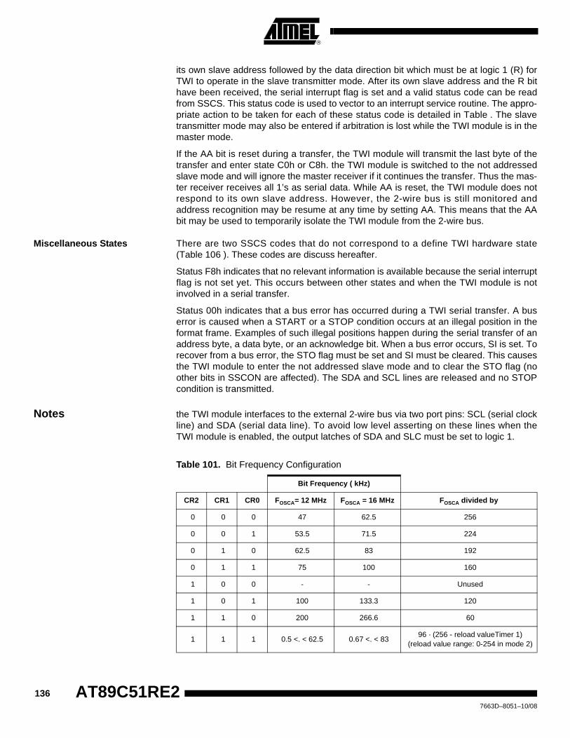
its own slave address followed by the data direction bit which must be at logic 1 (R) forTWI to operate in the slave transmitter mode. After its own slave address and the R bithave been received, the serial interrupt flag is set and a valid status code can be readfrom SSCS. This status code is used to vector to an interrupt service routine. The appro-priate action to be taken for each of these status code is detailed in Table . The slavetransmitter mode may also be entered if arbitration is lost while the TWI module is in themaster mode.
If the AA bit is reset during a transfer, the TWI module will transmit the last byte of thetransfer and enter state C0h or C8h. the TWI module is switched to the not addressedslave mode and will ignore the master receiver if it continues the transfer. Thus the mas-ter receiver receives all 1’s as serial data. While AA is reset, the TWI module does notrespond to its own slave address. However, the 2-wire bus is still monitored andaddress recognition may be resume at any time by setting AA. This means that the AAbit may be used to temporarily isolate the TWI module from the 2-wire bus.
Miscellaneous States There are two SSCS codes that do not correspond to a define TWI hardware state(Table 106 ). These codes are discuss hereafter.
Status F8h indicates that no relevant information is available because the serial interruptflag is not set yet. This occurs between other states and when the TWI module is notinvolved in a serial transfer.
Status 00h indicates that a bus error has occurred during a TWI serial transfer. A buserror is caused when a START or a STOP condition occurs at an illegal position in theformat frame. Examples of such illegal positions happen during the serial transfer of anaddress byte, a data byte, or an acknowledge bit. When a bus error occurs, SI is set. Torecover from a bus error, the STO flag must be set and SI must be cleared. This causesthe TWI module to enter the not addressed slave mode and to clear the STO flag (noother bits in SSCON are affected). The SDA and SCL lines are released and no STOPcondition is transmitted.
Notes the TWI module interfaces to the external 2-wire bus via two port pins: SCL (serial clockline) and SDA (serial data line). To avoid low level asserting on these lines when theTWI module is enabled, the output latches of SDA and SLC must be set to logic 1.
Table 101. Bit Frequency Configuration
Bit Frequency ( kHz)
CR2 CR1 CR0 FOSCA= 12 MHz FOSCA = 16 MHz FOSCA divided by
0 0 0 47 62.5 256
0 0 1 53.5 71.5 224
0 1 0 62.5 83 192
0 1 1 75 100 160
1 0 0 - - Unused
1 0 1 100 133.3 120
1 1 0 200 266.6 60
1 1 1 0.5 <. < 62.5 0.67 <. < 8396 · (256 - reload valueTimer 1)
(reload value range: 0-254 in mode 2)
136 AT89C51RE27663D–8051–10/08
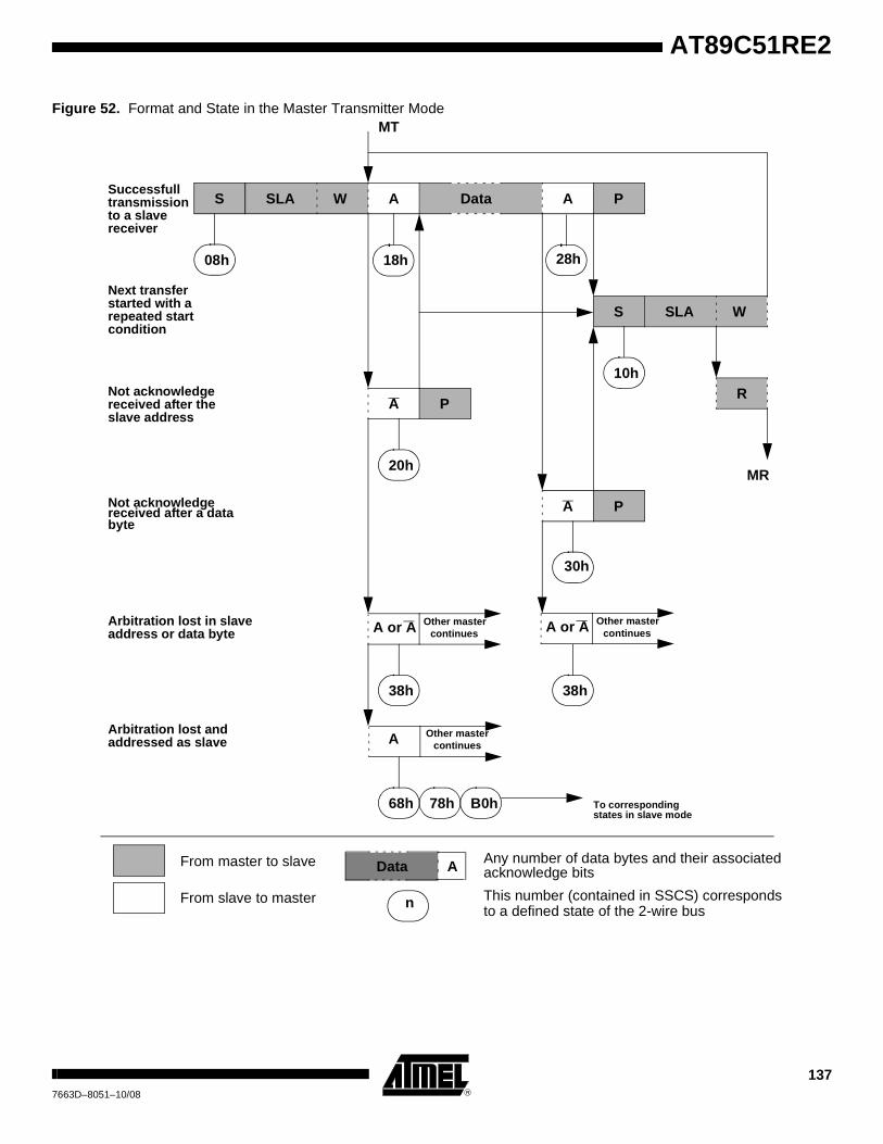
AT89C51RE2
Figure 52. Format and State in the Master Transmitter Mode
S SLA W A Data A P
08h 18h 28h
MT
S SLA W
A P
A P
R
MR
10h
20h
30h
A or A continues
38h38h
A continues
68h
Other master
Other master
78h B0h To corresponding states in slave mode
Successfulltransmissionto a slave receiver
Next transferstarted with arepeated startcondition
Not acknowledgereceived after theslave address
Not acknowledgereceived after a data
Arbitration lost in slaveaddress or data byte
Arbitration lost andaddressed as slave
byte
A or A continuesOther master
Data A
n
From master to slave
From slave to master
Any number of data bytes and their associatedacknowledge bits
This number (contained in SSCS) correspondsto a defined state of the 2-wire bus
1377663D–8051–10/08
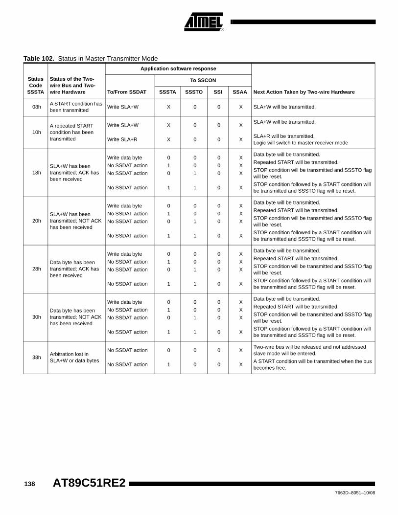
Table 102. Status in Master Transmitter Mode
Status Code
SSSTA
Status of the Two-wire Bus and Two-wire Hardware
Application software response
Next Action Taken by Two-wire HardwareTo/From SSDAT
To SSCON
SSSTA SSSTO SSI SSAA
08hA START condition has been transmitted
Write SLA+W X 0 0 X SLA+W will be transmitted.
10hA repeated START condition has been transmitted
Write SLA+W
Write SLA+R
X
X
0
0
0
0
X
X
SLA+W will be transmitted.
SLA+R will be transmitted.Logic will switch to master receiver mode
18hSLA+W has been transmitted; ACK has been received
Write data byte
No SSDAT action
No SSDAT action
No SSDAT action
0
1
0
1
0
0
1
1
0
0
0
0
X
X
X
X
Data byte will be transmitted.
Repeated START will be transmitted.
STOP condition will be transmitted and SSSTO flag will be reset.
STOP condition followed by a START condition will be transmitted and SSSTO flag will be reset.
20hSLA+W has been transmitted; NOT ACK has been received
Write data byte
No SSDAT action
No SSDAT action
No SSDAT action
0
1
0
1
0
0
1
1
0
0
0
0
X
X
X
X
Data byte will be transmitted.
Repeated START will be transmitted.
STOP condition will be transmitted and SSSTO flag will be reset.
STOP condition followed by a START condition will be transmitted and SSSTO flag will be reset.
28hData byte has been transmitted; ACK has been received
Write data byte
No SSDAT action
No SSDAT action
No SSDAT action
0
1
0
1
0
0
1
1
0
0
0
0
X
X
X
X
Data byte will be transmitted.
Repeated START will be transmitted.
STOP condition will be transmitted and SSSTO flag will be reset.
STOP condition followed by a START condition will be transmitted and SSSTO flag will be reset.
30hData byte has been transmitted; NOT ACK has been received
Write data byte
No SSDAT action
No SSDAT action
No SSDAT action
0
1
0
1
0
0
1
1
0
0
0
0
X
X
X
X
Data byte will be transmitted.
Repeated START will be transmitted.
STOP condition will be transmitted and SSSTO flag will be reset.
STOP condition followed by a START condition will be transmitted and SSSTO flag will be reset.
38hArbitration lost in SLA+W or data bytes
No SSDAT action
No SSDAT action
0
1
0
0
0
0
X
X
Two-wire bus will be released and not addressed slave mode will be entered.
A START condition will be transmitted when the bus becomes free.
138 AT89C51RE27663D–8051–10/08
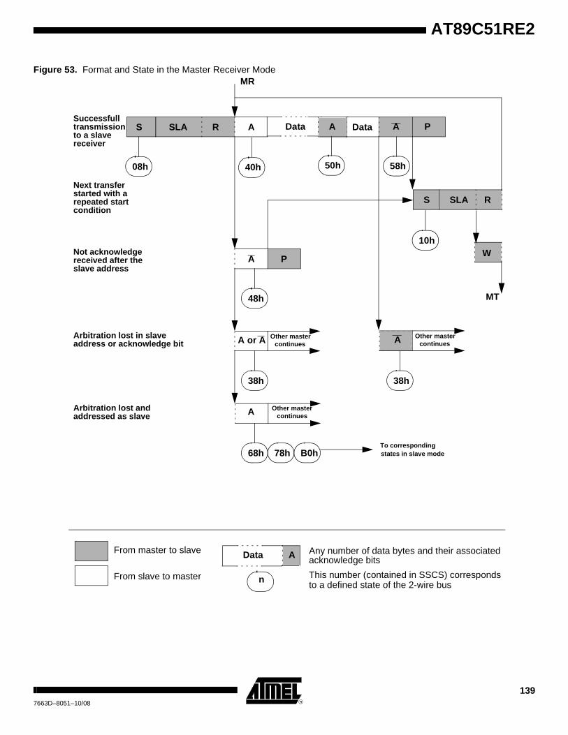
AT89C51RE2
Figure 53. Format and State in the Master Receiver Mode
S SLA R A Data
08h 40h 58h
S SLA R
A PW
MT
10h
48h
A or A continues
38h38h
A continues
68h
Other master
Other master
78h B0hTo corresponding states in slave mode
Successfulltransmissionto a slave receiver
Next transferstarted with arepeated startcondition
Not acknowledgereceived after theslave address
Arbitration lost andaddressed as slave
A continuesOther master
n
From master to slave
From slave to master
Any number of data bytes and their associatedacknowledge bits
This number (contained in SSCS) correspondsto a defined state of the 2-wire bus
A Data PA
50h
MR
Arbitration lost in slaveaddress or acknowledge bit
Data A
1397663D–8051–10/08

Table 103. Status in Master Receiver Mode
Status Code
SSSTA
Status of the Two-wire Bus and Two-wire Hardware
Application software response
Next Action Taken by Two-wire HardwareTo/From SSDAT
To SSCON
SSSTA SSSTO SSI SSAA
08hA START condition has been transmitted
Write SLA+R X 0 0 X SLA+R will be transmitted.
10hA repeated START condition has been transmitted
Write SLA+R
Write SLA+W
X
X
0
0
0
0
X
X
SLA+R will be transmitted.
SLA+W will be transmitted.Logic will switch to master transmitter mode.
38hArbitration lost in SLA+R or NOT ACK bit
No SSDAT action
No SSDAT action
0
1
0
0
0
0
X
X
Two-wire bus will be released and not addressed slave mode will be entered.
A START condition will be transmitted when the bus becomes free.
40hSLA+R has been transmitted; ACK has been received
No SSDAT action
No SSDAT action
0
0
0
0
0
0
0
1
Data byte will be received and NOT ACK will be returned.
Data byte will be received and ACK will be returned.
48hSLA+R has been transmitted; NOT ACK has been received
No SSDAT action
No SSDAT action
No SSDAT action
1
0
1
0
1
1
0
0
0
X
X
X
Repeated START will be transmitted.
STOP condition will be transmitted and SSSTO flag will be reset.
STOP condition followed by a START condition will be transmitted and SSSTO flag will be reset.
50hData byte has been received; ACK has been returned
Read data byte
Read data byte
0
0
0
0
0
0
0
1
Data byte will be received and NOT ACK will be returned.
Data byte will be received and ACK will be returned.
58hData byte has been received; NOT ACK has been returned
Read data byte
Read data byte
Read data byte
1
0
1
0
1
1
0
0
0
X
X
X
Repeated START will be transmitted.
STOP condition will be transmitted and SSSTO flag will be reset.
STOP condition followed by a START condition will be transmitted and SSSTO flag will be reset.
140 AT89C51RE27663D–8051–10/08
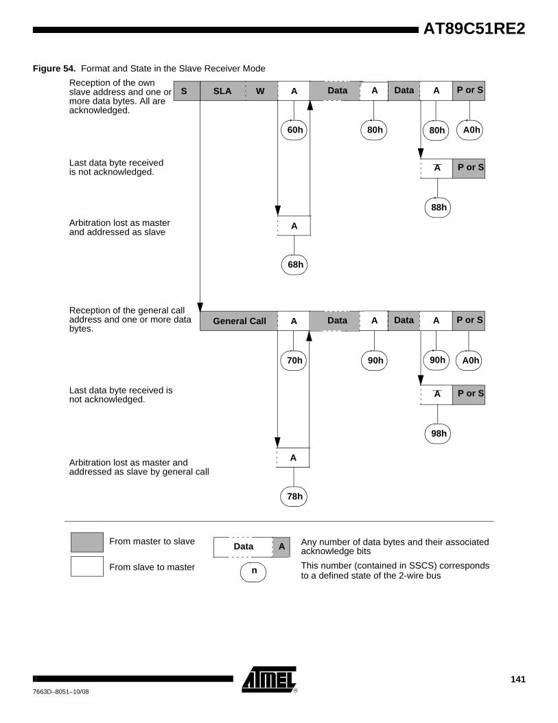
AT89C51RE2
Figure 54. Format and State in the Slave Receiver Mode
S SLA W A Data A Data P or SA
P or SA
General Call A Data A Data P or SA
A
60h
68h
80h 80h A0h
88h
70h 90h 90h A0h
P or SA
98h
A
78h
Data A
n
From master to slave
From slave to master
Any number of data bytes and their associatedacknowledge bits
This number (contained in SSCS) correspondsto a defined state of the 2-wire bus
Reception of the own slave address and one ormore data bytes. All areacknowledged.
Last data byte receivedis not acknowledged.
Arbitration lost as masterand addressed as slave
Reception of the general calladdress and one or more databytes.
Last data byte received isnot acknowledged.
Arbitration lost as master andaddressed as slave by general call
1417663D–8051–10/08
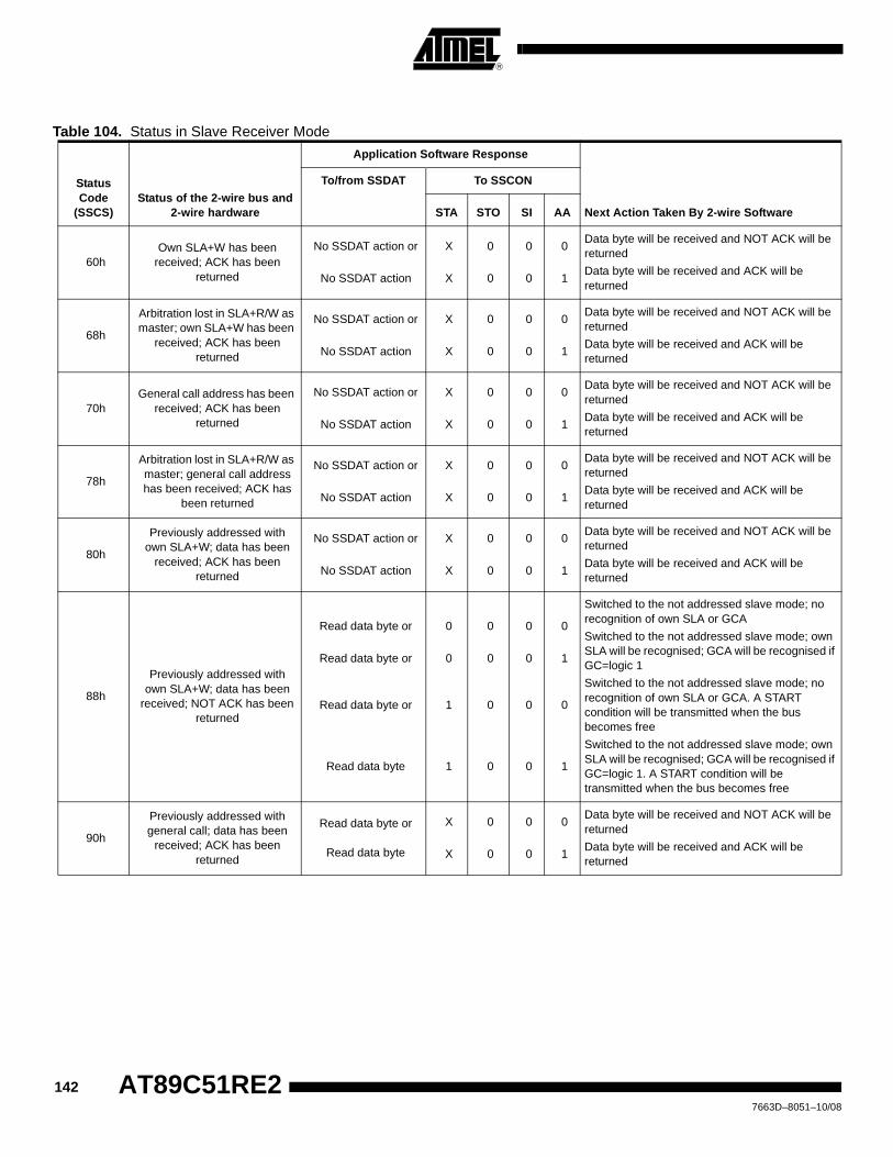
Table 104. Status in Slave Receiver Mode
Status Code
(SSCS)Status of the 2-wire bus and
2-wire hardware
Application Software Response
Next Action Taken By 2-wire Software
To/from SSDAT To SSCON
STA STO SI AA
60hOwn SLA+W has been
received; ACK has been returned
No SSDAT action or
No SSDAT action
X
X
0
0
0
0
0
1
Data byte will be received and NOT ACK will be returned
Data byte will be received and ACK will be returned
68h
Arbitration lost in SLA+R/W as master; own SLA+W has been
received; ACK has been returned
No SSDAT action or
No SSDAT action
X
X
0
0
0
0
0
1
Data byte will be received and NOT ACK will be returned
Data byte will be received and ACK will be returned
70hGeneral call address has been
received; ACK has been returned
No SSDAT action or
No SSDAT action
X
X
0
0
0
0
0
1
Data byte will be received and NOT ACK will be returned
Data byte will be received and ACK will be returned
78h
Arbitration lost in SLA+R/W as master; general call address has been received; ACK has
been returned
No SSDAT action or
No SSDAT action
X
X
0
0
0
0
0
1
Data byte will be received and NOT ACK will be returned
Data byte will be received and ACK will be returned
80h
Previously addressed with own SLA+W; data has been
received; ACK has been returned
No SSDAT action or
No SSDAT action
X
X
0
0
0
0
0
1
Data byte will be received and NOT ACK will be returned
Data byte will be received and ACK will be returned
88h
Previously addressed with own SLA+W; data has been
received; NOT ACK has been returned
Read data byte or
Read data byte or
Read data byte or
Read data byte
0
0
1
1
0
0
0
0
0
0
0
0
0
1
0
1
Switched to the not addressed slave mode; no recognition of own SLA or GCA
Switched to the not addressed slave mode; own SLA will be recognised; GCA will be recognised if GC=logic 1
Switched to the not addressed slave mode; no recognition of own SLA or GCA. A START condition will be transmitted when the bus becomes free
Switched to the not addressed slave mode; own SLA will be recognised; GCA will be recognised if GC=logic 1. A START condition will be transmitted when the bus becomes free
90h
Previously addressed with general call; data has been
received; ACK has been returned
Read data byte or
Read data byte
X
X
0
0
0
0
0
1
Data byte will be received and NOT ACK will be returned
Data byte will be received and ACK will be returned
142 AT89C51RE27663D–8051–10/08
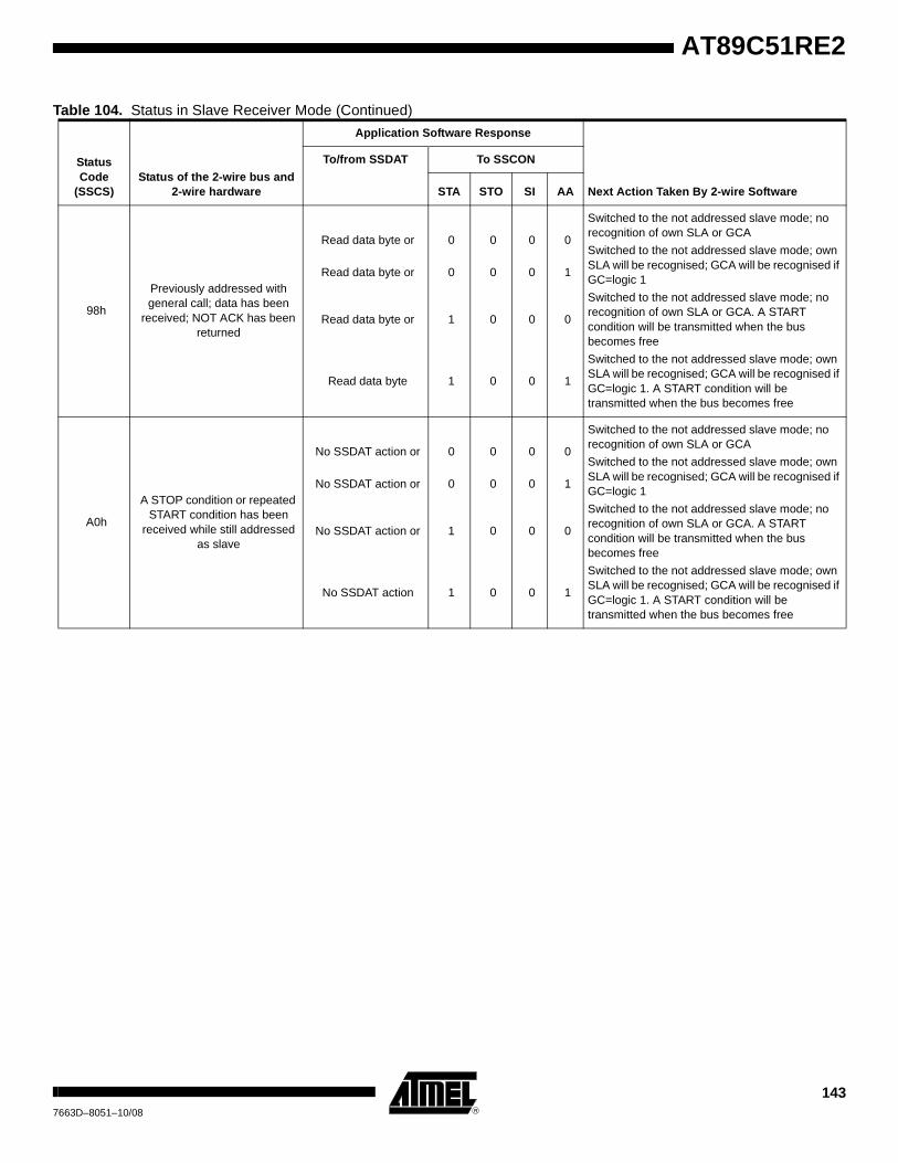
AT89C51RE2
98h
Previously addressed with general call; data has been
received; NOT ACK has been returned
Read data byte or
Read data byte or
Read data byte or
Read data byte
0
0
1
1
0
0
0
0
0
0
0
0
0
1
0
1
Switched to the not addressed slave mode; no recognition of own SLA or GCA
Switched to the not addressed slave mode; own SLA will be recognised; GCA will be recognised if GC=logic 1
Switched to the not addressed slave mode; no recognition of own SLA or GCA. A START condition will be transmitted when the bus becomes free
Switched to the not addressed slave mode; own SLA will be recognised; GCA will be recognised if GC=logic 1. A START condition will be transmitted when the bus becomes free
A0h
A STOP condition or repeated START condition has been
received while still addressed as slave
No SSDAT action or
No SSDAT action or
No SSDAT action or
No SSDAT action
0
0
1
1
0
0
0
0
0
0
0
0
0
1
0
1
Switched to the not addressed slave mode; no recognition of own SLA or GCA
Switched to the not addressed slave mode; own SLA will be recognised; GCA will be recognised if GC=logic 1
Switched to the not addressed slave mode; no recognition of own SLA or GCA. A START condition will be transmitted when the bus becomes free
Switched to the not addressed slave mode; own SLA will be recognised; GCA will be recognised if GC=logic 1. A START condition will be transmitted when the bus becomes free
Table 104. Status in Slave Receiver Mode (Continued)
Status Code
(SSCS)Status of the 2-wire bus and
2-wire hardware
Application Software Response
Next Action Taken By 2-wire Software
To/from SSDAT To SSCON
STA STO SI AA
1437663D–8051–10/08
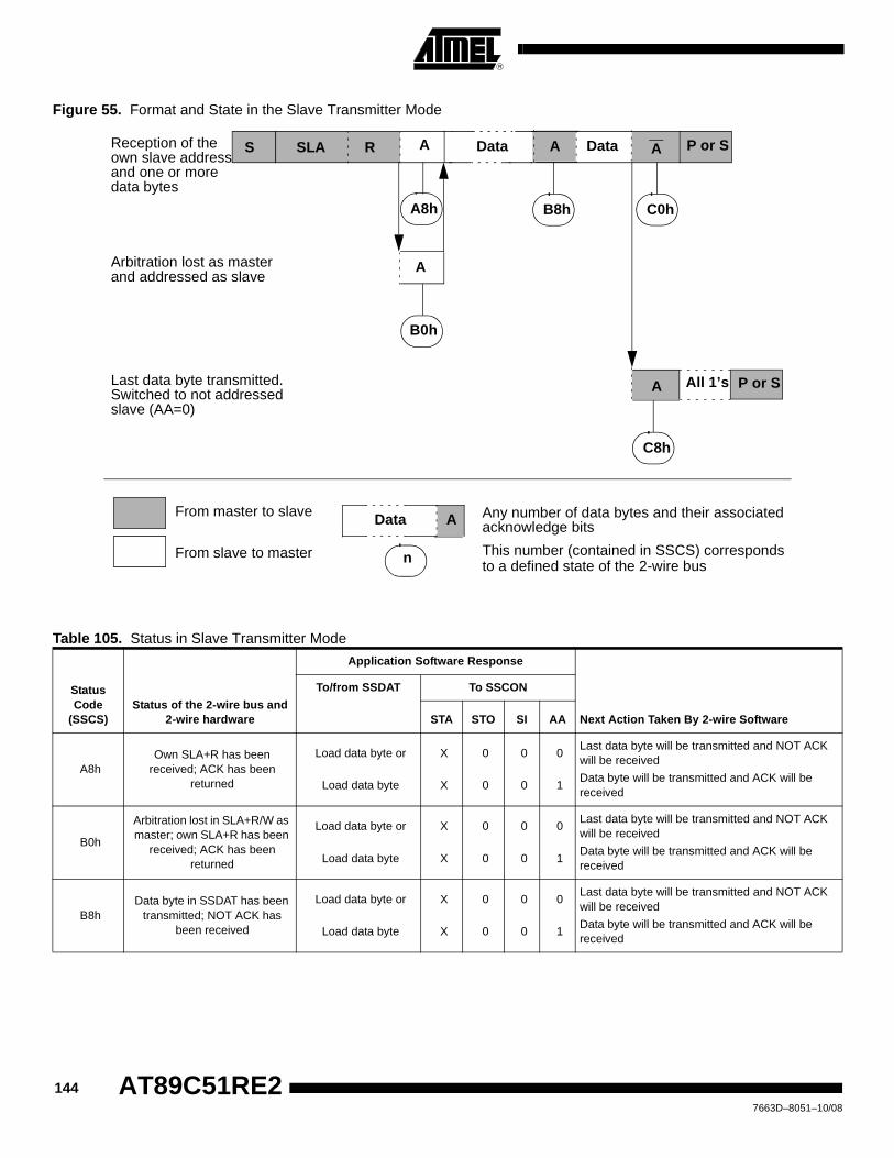
Figure 55. Format and State in the Slave Transmitter Mode
S SLA R A Data A Data P or SA
A8h B8h C0h
P or SA
C8h
All 1’s
A
B0h
Data A
n
From master to slave
From slave to master
Any number of data bytes and their associatedacknowledge bits
This number (contained in SSCS) correspondsto a defined state of the 2-wire bus
Reception of the own slave addressand one or more data bytes
Arbitration lost as masterand addressed as slave
Last data byte transmitted.Switched to not addressedslave (AA=0)
Table 105. Status in Slave Transmitter Mode
Status Code
(SSCS)Status of the 2-wire bus and
2-wire hardware
Application Software Response
Next Action Taken By 2-wire Software
To/from SSDAT To SSCON
STA STO SI AA
A8hOwn SLA+R has been
received; ACK has been returned
Load data byte or
Load data byte
X
X
0
0
0
0
0
1
Last data byte will be transmitted and NOT ACK will be received
Data byte will be transmitted and ACK will be received
B0h
Arbitration lost in SLA+R/W as master; own SLA+R has been
received; ACK has been returned
Load data byte or
Load data byte
X
X
0
0
0
0
0
1
Last data byte will be transmitted and NOT ACK will be received
Data byte will be transmitted and ACK will be received
B8hData byte in SSDAT has been
transmitted; NOT ACK has been received
Load data byte or
Load data byte
X
X
0
0
0
0
0
1
Last data byte will be transmitted and NOT ACK will be received
Data byte will be transmitted and ACK will be received
144 AT89C51RE27663D–8051–10/08

AT89C51RE2
Table 106. Miscellaneous Status
C0hData byte in SSDAT has been
transmitted; NOT ACK has been received
No SSDAT action or
No SSDAT action or
No SSDAT action or
No SSDAT action
0
0
1
1
0
0
0
0
0
0
0
0
0
1
0
1
Switched to the not addressed slave mode; no recognition of own SLA or GCA
Switched to the not addressed slave mode; own SLA will be recognised; GCA will be recognised if GC=logic 1
Switched to the not addressed slave mode; no recognition of own SLA or GCA. A START condition will be transmitted when the bus becomes free
Switched to the not addressed slave mode; own SLA will be recognised; GCA will be recognised if GC=logic 1. A START condition will be transmitted when the bus becomes free
C8hLast data byte in SSDAT has
been transmitted (AA=0); ACK has been received
No SSDAT action or
No SSDAT action or
No SSDAT action or
No SSDAT action
0
0
1
1
0
0
0
0
0
0
0
0
0
1
0
1
Switched to the not addressed slave mode; no recognition of own SLA or GCA
Switched to the not addressed slave mode; own SLA will be recognised; GCA will be recognised if GC=logic 1
Switched to the not addressed slave mode; no recognition of own SLA or GCA. A START condition will be transmitted when the bus becomes free
Switched to the not addressed slave mode; own SLA will be recognised; GCA will be recognised if GC=logic 1. A START condition will be transmitted when the bus becomes free
Table 105. Status in Slave Transmitter Mode (Continued)
Status Code
(SSCS)Status of the 2-wire bus and
2-wire hardware
Application Software Response
Next Action Taken By 2-wire Software
To/from SSDAT To SSCON
STA STO SI AA
Status Code
(SSCS)
Status of the 2-wire bus and 2-wire
hardware
Application Software Response
Next Action Taken By 2-wire Software
To/from SSDAT
To SSCON
STA STO SI AA
F8hNo relevant state
information available; SI= 0
No SSDAT action
No SSCON action Wait or proceed current transfer
00hBus error due to an
illegal START or STOP condition
No SSDAT action
0 1 0 X
Only the internal hardware is affected, no STOP condition is sent on the bus. In all cases, the bus is released and STO is reset.
1457663D–8051–10/08
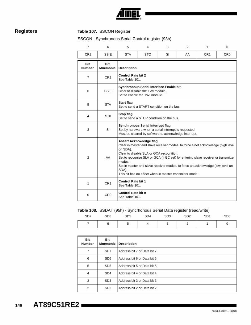
Registers Table 107. SSCON Register
SSCON - Synchronous Serial Control register (93h)
7 6 5 4 3 2 1 0
CR2 SSIE STA STO SI AA CR1 CR0
Bit Number
Bit Mnemonic Description
7 CR2Control Rate bit 2See Table 101.
6 SSIESynchronous Serial Interface Enable bitClear to disable the TWI module.Set to enable the TWI module.
5 STAStart flagSet to send a START condition on the bus.
4 ST0Stop flagSet to send a STOP condition on the bus.
3 SISynchronous Serial Interrupt flagSet by hardware when a serial interrupt is requested.Must be cleared by software to acknowledge interrupt.
2 AA
Assert Acknowledge flagClear in master and slave receiver modes, to force a not acknowledge (high level on SDA).Clear to disable SLA or GCA recognition.Set to recognise SLA or GCA (if GC set) for entering slave receiver or transmitter modes.Set in master and slave receiver modes, to force an acknowledge (low level on SDA).This bit has no effect when in master transmitter mode.
1 CR1Control Rate bit 1See Table 101.
0 CR0Control Rate bit 0See Table 101.
Table 108. SSDAT (95h) - Syncrhonous Serial Data register (read/write)SD7 SD6 SD5 SD4 SD3 SD2 SD1 SD0
7 6 5 4 3 2 1 0
Bit Number
Bit Mnemonic Description
7 SD7 Address bit 7 or Data bit 7.
6 SD6 Address bit 6 or Data bit 6.
5 SD5 Address bit 5 or Data bit 5.
4 SD4 Address bit 4 or Data bit 4.
3 SD3 Address bit 3 or Data bit 3.
2 SD2 Address bit 2 or Data bit 2.
146 AT89C51RE27663D–8051–10/08

AT89C51RE2
Table 111. SSADR (096h) - Synchronus Serial Address Register (read/write)
Table 112. SSADR Register - Reset value = FEh
1 SD1 Address bit 1 or Data bit 1.
0 SD0 Address bit 0 (R/W) or Data bit 0.
Table 109. SSCS (094h) read - Synchronous Serial Control and Status Register7 6 5 4 3 2 1 0
SC4 SC3 SC2 SC1 SC0 0 0 0
Table 110. SSCS Register: Read Mode - Reset Value = F8hBit
NumberBit
Mnemonic Description
0 0 Always zero
1 0 Always zero
2 0 Always zero
3 SC0Status Code bit 0See to Table 106.
4 SC1Status Code bit 1
See to Table 106.
5 SC2Status Code bit 2See to Table 106.
6 SC3Status Code bit 3See to Table 106.
7 SC4Status Code bit 4See to Table 106.
7 6 5 4 3 2 1 0
A7 A6 A5 A4 A3 A2 A1 A0
Bit Number
Bit Mnemonic Description
7 A7 Slave Address bit 7
6 A6 Slave Address bit 6
5 A5 Slave Address bit 5
4 A4 Slave Address bit 4
3 A3 Slave Address bit 3
2 A2 Slave Address bit 2
1 A1 Slave Address bit 1
Bit Number
Bit Mnemonic Description
1477663D–8051–10/08

0 GC
General Call bit
Clear to disable the general call address recognition.
Set to enable the general call address recognition.
Bit Number
Bit Mnemonic Description
148 AT89C51RE27663D–8051–10/08
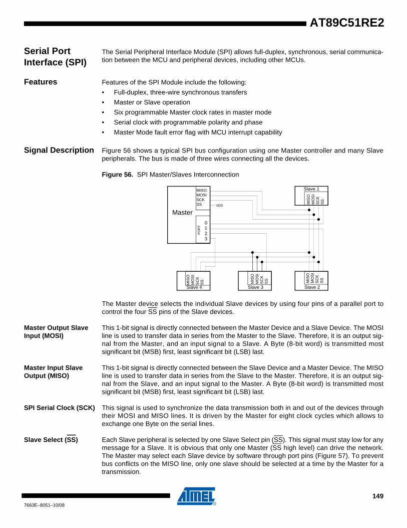
AT89C51RE2
Serial Port Interface (SPI)
The Serial Peripheral Interface Module (SPI) allows full-duplex, synchronous, serial communica-tion between the MCU and peripheral devices, including other MCUs.
Features Features of the SPI Module include the following:
• Full-duplex, three-wire synchronous transfers
• Master or Slave operation
• Six programmable Master clock rates in master mode
• Serial clock with programmable polarity and phase
• Master Mode fault error flag with MCU interrupt capability
Signal Description Figure 56 shows a typical SPI bus configuration using one Master controller and many Slaveperipherals. The bus is made of three wires connecting all the devices.
Figure 56. SPI Master/Slaves Interconnection
The Master device selects the individual Slave devices by using four pins of a parallel port tocontrol the four SS pins of the Slave devices.
Master Output Slave Input (MOSI)
This 1-bit signal is directly connected between the Master Device and a Slave Device. The MOSIline is used to transfer data in series from the Master to the Slave. Therefore, it is an output sig-nal from the Master, and an input signal to a Slave. A Byte (8-bit word) is transmitted mostsignificant bit (MSB) first, least significant bit (LSB) last.
Master Input Slave Output (MISO)
This 1-bit signal is directly connected between the Slave Device and a Master Device. The MISOline is used to transfer data in series from the Slave to the Master. Therefore, it is an output sig-nal from the Slave, and an input signal to the Master. A Byte (8-bit word) is transmitted mostsignificant bit (MSB) first, least significant bit (LSB) last.
SPI Serial Clock (SCK) This signal is used to synchronize the data transmission both in and out of the devices throughtheir MOSI and MISO lines. It is driven by the Master for eight clock cycles which allows toexchange one Byte on the serial lines.
Slave Select (SS) Each Slave peripheral is selected by one Slave Select pin (SS). This signal must stay low for anymessage for a Slave. It is obvious that only one Master (SS high level) can drive the network.The Master may select each Slave device by software through port pins (Figure 57). To preventbus conflicts on the MISO line, only one slave should be selected at a time by the Master for atransmission.
Slave 1
MIS
OM
OS
IS
CK
SS
MISOMOSISCKSS
PO
RT
0123
Slave 3
MIS
OM
OS
IS
CK
SS
Slave 4
MIS
OM
OS
IS
CK
SS
Slave 2
MIS
OM
OS
IS
CK
SS
VDD
Master
1497663E–8051–10/08
In a Master configuration, the SS line can be used in conjunction with the MODF flag in the SPIStatus register (SPSCR) to prevent multiple masters from driving MOSI and SCK (see Errorconditions).
A high level on the SS pin puts the MISO line of a Slave SPI in a high-impedance state.
The SS pin could be used as a general-purpose if the following conditions are met:
• The device is configured as a Master and the SSDIS control bit in SPCON is set. This kind of configuration can be found when only one Master is driving the network and there is no way that the SS pin could be pulled low. Therefore, the MODF flag in the SPSCR will never be set(1).
• The Device is configured as a Slave with CPHA and SSDIS control bits set(2). This kind of configuration can happen when the system includes one Master and one Slave only. Therefore, the device should always be selected and there is no reason that the Master uses the SS pin to select the communicating Slave device.
Note: 1. Clearing SSDIS control bit does not clear MODF.
2. Special care should be taken not to set SSDIS control bit when CPHA =’0’ because in thismode, the SS is used to start the transmission.
Baud Rate In Master mode, the baud rate can be selected from a baud rate generator which is controlled bythree bits in the SPCON register: SPR2, SPR1 and SPR0.The Master clock is selected from oneof seven clock rates resulting from the division of the internal clock by 4, 8, 16, 32, 64 or 128.
Table 113 gives the different clock rates selected by SPR2:SPR1:SPR0.
In Slave mode, the maximum baud rate allowed on the SCK input is limited to Fsys/4
Table 113. SPI Master Baud Rate Selection
SPR2 SPR1 SPR0 Clock Rate Baud Rate Divisor (BD)
0 0 0 Don’t Use No BRG
0 0 1 FCLK PERIPH /4 4
0 1 0 FCLK PERIPH/8 8
0 1 1 FCLK PERIPH /16 16
1 0 0 FCLK PERIPH /32 32
1 0 1 FCLK PERIPH /64 64
1 1 0 FCLK PERIPH /128 128
1 1 1 Don’t Use No BRG
1507663E–8051–10/08
AT89C51RE2
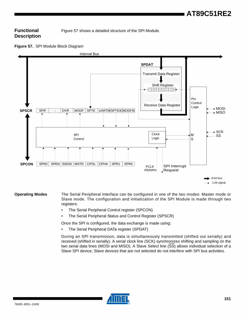
AT89C51RE2
Functional Description
Figure 57 shows a detailed structure of the SPI Module.
Figure 57. SPI Module Block Diagram
Operating Modes The Serial Peripheral Interface can be configured in one of the two modes: Master mode orSlave mode. The configuration and initialization of the SPI Module is made through tworegisters:
• The Serial Peripheral Control register (SPCON)
• The Serial Peripheral Status and Control Register (SPSCR)
Once the SPI is configured, the data exchange is made using:
• The Serial Peripheral DATa register (SPDAT)
During an SPI transmission, data is simultaneously transmitted (shifted out serially) andreceived (shifted in serially). A serial clock line (SCK) synchronizes shifting and sampling on thetwo serial data lines (MOSI and MISO). A Slave Select line (SS) allows individual selection of aSlave SPI device; Slave devices that are not selected do not interfere with SPI bus activities.
Shift Register01234567
Internal Bus
PinControlLogic
MISOMOSI
SCKMS
ClockLogic
SPI Interrupt
8-bit bus
1-bit signal
SS
FCLK
Receive Data Register
SPDAT
SPIControl
Transmit Data Register
- MODFSPIF OVR SPTE UARTM SPTEIEMODFIESPSCR
SPEN MSTRSPR2 SSDIS CPOL CPHA SPR1 SPR0SPCON
Request PERIPH
1517663E–8051–10/08

When the Master device transmits data to the Slave device via the MOSI line, the Slave deviceresponds by sending data to the Master device via the MISO line. This implies full-duplex trans-mission with both data out and data in synchronized with the same clock (Figure 58).
Figure 58. Full-Duplex Master-Slave Interconnection
Master Mode The SPI operates in Master mode when the Master bit, MSTR (1), in the SPCON register is set.Only one Master SPI device can initiate transmissions. Software begins the transmission from aMaster SPI Module by writing to the Serial Peripheral Data Register (SPDAT). If the shift registeris empty, the Byte is immediately transferred to the shift register. The Byte begins shifting out onMOSI pin under the control of the serial clock, SCK. Simultaneously, another Byte shifts in fromthe Slave on the Master’s MISO pin. The transmission ends when the Serial Peripheral transferdata flag, SPIF, in SPSCR becomes set. At the same time that SPIF becomes set, the receivedByte from the Slave is transferred to the receive data register in SPDAT. Software clears SPIFby reading the Serial Peripheral Status register (SPSCR) with the SPIF bit set, and then readingthe SPDAT.
Slave Mode The SPI operates in Slave mode when the Master bit, MSTR (2), in the SPCON register iscleared. Before a data transmission occurs, the Slave Select pin, SS, of the Slave device mustbe set to’0’. SS must remain low until the transmission is complete.
In a Slave SPI Module, data enters the shift register under the control of the SCK from the Mas-ter SPI Module. After a Byte enters the shift register, it is immediately transferred to the receivedata register in SPDAT, and the SPIF bit is set. To prevent an overflow condition, Slave softwaremust then read the SPDAT before another Byte enters the shift register (3). A Slave SPI mustcomplete the write to the SPDAT (shift register) at least one bus cycle before the Master SPIstarts a transmission. If the write to the data register is late, the SPI transmits the data already inthe shift register from the previous transmission.
Transmission Formats Software can select any of four combinations of serial clock (SCK) phase and polarity using twobits in the SPCON: the Clock Polarity (CPOL (4)) and the Clock Phase (CPHA4). CPOL definesthe default SCK line level in idle state. It has no significant effect on the transmission format.CPHA defines the edges on which the input data are sampled and the edges on which the out-put data are shifted (Figure 59 and Figure 60). The clock phase and polarity should be identicalfor the Master SPI device and the communicating Slave device.
8-bit Shift register
SPI Clock Generator
Master MCU
8-bit Shift registerMISOMISO
MOSI MOSI
SCK SCK
VSS
VDD SSSS
Slave MCU
1. The SPI Module should be configured as a Master before it is enabled (SPEN set). Also, the Mas-ter SPI should be configured before the Slave SPI.
2. The SPI Module should be configured as a Slave before it is enabled (SPEN set). 3. The maximum frequency of the SCK for an SPI configured as a Slave is the bus clock speed. 4. Before writing to the CPOL and CPHA bits, the SPI should be disabled (SPEN =’0’).
1527663E–8051–10/08
AT89C51RE2

AT89C51RE2
Figure 59. Data Transmission Format (CPHA = 0)
Figure 60. Data Transmission Format (CPHA = 1)
Figure 61. CPHA/SS Timing
As shown in Figure 59, the first SCK edge is the MSB capture strobe. Therefore, the Slave mustbegin driving its data before the first SCK edge, and a falling edge on the SS pin is used to startthe transmission. The SS pin must be toggled high and then low between each Byte transmitted(Figure 61).
Figure 60 shows an SPI transmission in which CPHA is’1’. In this case, the Master begins driv-ing its MOSI pin on the first SCK edge. Therefore, the Slave uses the first SCK edge as a starttransmission signal. The SS pin can remain low between transmissions (Figure 61). This formatmay be preferred in systems having only one Master and only one Slave driving the MISO dataline.
Queuing transmission For an SPI configured in master or slave mode, a queued data byte must be transmit-ted/received immediately after the previous transmission has completed.
MSB bit6 bit5 bit4 bit3 bit2 bit1 LSB
bit6 bit5 bit4 bit3 bit2 bit1MSB LSB
1 32 4 5 6 7 8
Capture Point
SS (to Slave)
MISO (from Slave)
MOSI (from Master)
SCK (CPOL = 1)
SCK (CPOL = 0)
SPEN (Internal)
SCK Cycle Number
MSB bit6 bit5 bit4 bit3 bit2 bit1 LSB
bit6 bit5 bit4 bit3 bit2 bit1MSB LSB
1 32 4 5 6 7 8
Capture Point
SS (to Slave)
MISO (from Slave)
MOSI (from Master)
SCK (CPOL = 1)
SCK (CPOL = 0)
SPEN (Internal)
SCK Cycle Number
Byte 1 Byte 2 Byte 3MISO/MOSI
Master SS
Slave SS(CPHA = 1)
Slave SS(CPHA = 0)
1537663E–8051–10/08
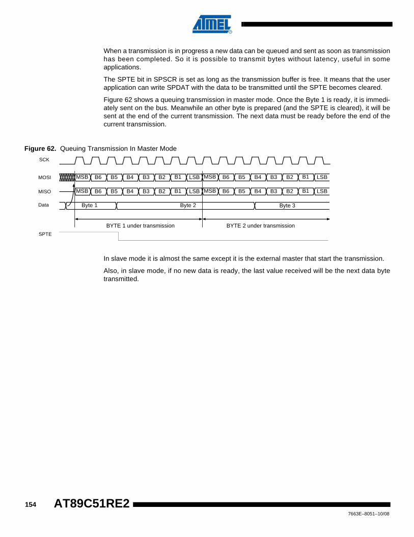
When a transmission is in progress a new data can be queued and sent as soon as transmissionhas been completed. So it is possible to transmit bytes without latency, useful in someapplications.
The SPTE bit in SPSCR is set as long as the transmission buffer is free. It means that the userapplication can write SPDAT with the data to be transmitted until the SPTE becomes cleared.
Figure 62 shows a queuing transmission in master mode. Once the Byte 1 is ready, it is immedi-ately sent on the bus. Meanwhile an other byte is prepared (and the SPTE is cleared), it will besent at the end of the current transmission. The next data must be ready before the end of thecurrent transmission.
Figure 62. Queuing Transmission In Master Mode
In slave mode it is almost the same except it is the external master that start the transmission.
Also, in slave mode, if no new data is ready, the last value received will be the next data bytetransmitted.
MSB B6 B5 B4 B3 B2 B1 LSBMOSI
SCK
MSB B6 B5 B4 B3 B2 B1 LSB
BYTE 1 under transmission
MSB B6 B5 B4 B3 B2 B1 LSB MSB B6 B5 B4 B3 B2 B1 LSBMISO
Data Byte 1 Byte 2 Byte 3
SPTE
BYTE 2 under transmission
1547663E–8051–10/08
AT89C51RE2
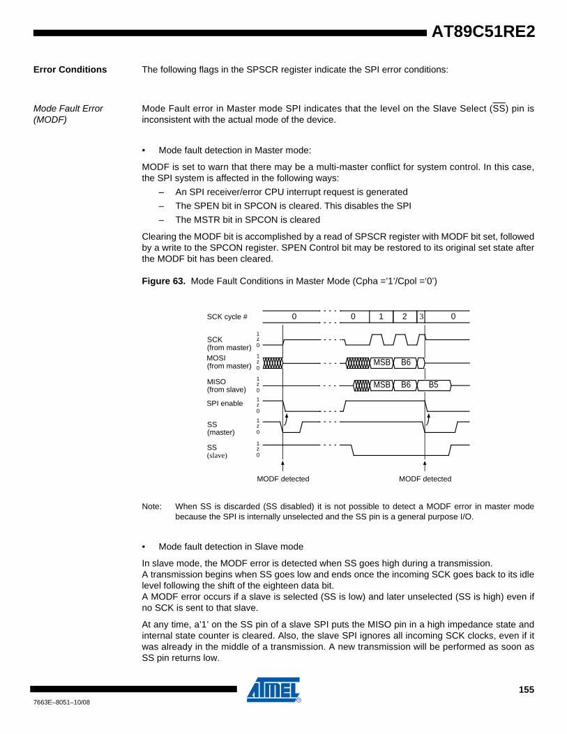
AT89C51RE2
Error Conditions The following flags in the SPSCR register indicate the SPI error conditions:
Mode Fault Error (MODF)
Mode Fault error in Master mode SPI indicates that the level on the Slave Select (SS) pin isinconsistent with the actual mode of the device.
• Mode fault detection in Master mode:
MODF is set to warn that there may be a multi-master conflict for system control. In this case,the SPI system is affected in the following ways:
– An SPI receiver/error CPU interrupt request is generated
– The SPEN bit in SPCON is cleared. This disables the SPI
– The MSTR bit in SPCON is cleared
Clearing the MODF bit is accomplished by a read of SPSCR register with MODF bit set, followedby a write to the SPCON register. SPEN Control bit may be restored to its original set state afterthe MODF bit has been cleared.
Figure 63. Mode Fault Conditions in Master Mode (Cpha =’1’/Cpol =’0’)
Note: When SS is discarded (SS disabled) it is not possible to detect a MODF error in master modebecause the SPI is internally unselected and the SS pin is a general purpose I/O.
• Mode fault detection in Slave mode
In slave mode, the MODF error is detected when SS goes high during a transmission.A transmission begins when SS goes low and ends once the incoming SCK goes back to its idlelevel following the shift of the eighteen data bit.A MODF error occurs if a slave is selected (SS is low) and later unselected (SS is high) even ifno SCK is sent to that slave.
At any time, a’1’ on the SS pin of a slave SPI puts the MISO pin in a high impedance state andinternal state counter is cleared. Also, the slave SPI ignores all incoming SCK clocks, even if itwas already in the middle of a transmission. A new transmission will be performed as soon asSS pin returns low.
SCK
SS(master)
1 2 3SCK cycle # 0 0
SS(slave)
(from master)
MODF detected
B6MSB
B6MSB
0z1
0z1
0z1
0z1
0z1
0
0z1
SPI enable
MODF detected
MOSI
MISO
(from master)
(from slave)B5
1557663E–8051–10/08
Figure 64. Mode Fault Conditions in Slave Mode
Note: when SS is discarded (SS disabled) it is not possible to detect a MODF error in slave modebecause the SPI is internally selected. Also the SS pin becomes a general purpose I/O.
OverRun Condition This error mean that the speed is not adapted for the running application:
An OverRun condition occurs when a byte has been received whereas the previous one has notbeen read by the application yet.The last byte (which generate the overrun error) does not overwrite the unread data so that itcan still be read. Therefore, an overrun error always indicates the loss of data.
Interrupts Three SPI status flags can generate a CPU interrupt requests:
Table 114. SPI Interrupts
Serial Peripheral data transfer flag, SPIF: This bit is set by hardware when a transfer has beencompleted. SPIF bit generates transmitter CPU interrupt request only when SPTEIE is disabled.
Mode Fault flag, MODF: This bit is set to indicate that the level on the SS is inconsistent with themode of the SPI (in both master and slave modes).
Serial Peripheral Transmit Register empty flag, SPTE: This bit is set when the transmit buffer isempty (other data can be loaded is SPDAT). SPTE bit generates transmitter CPU interruptrequest only when SPTEIE is enabled.
Note: While using SPTE interruption for “burst mode” transfers (SPTEIE=’1’), the user soft-ware application should take care to clear SPTEIE, during the last but one data reception (tobe able to generate an interrupt on SPIF flag at the end of the last data reception).
SCK
1 2 3SCK cycle # 0
SS(slave)
(from master)
MODF detected
B6MSB
B6MSB
0z1
0z1
0z1
0z1
0
MODF detected
MOSI
MISO
(from master)
(from slave)MSB
B5 B4
4
Flag Request
SPIF (SPI data transfer) SPI Transmitter Interrupt Request
MODF (Mode Fault) SPI mode-fault Interrupt Request
SPTE (Transmit register empty) SPI transmit register empty Interrupt Request
1567663E–8051–10/08
AT89C51RE2
AT89C51RE2
Figure 65. SPI Interrupt Requests Generation
Registers Three registers in the SPI module provide control, status and data storage functions. These reg-isters are describe in the following paragraphs.
Serial Peripheral Control Register (SPCON)
• The Serial Peripheral Control Register does the following:
• Selects one of the Master clock rates
• Configure the SPI Module as Master or Slave
• Selects serial clock polarity and phase
• Enables the SPI Module
• Frees the SS pin for a general-purpose
Table 115 describes this register and explains the use of each bit
Table 115. SPCON Register
SPCON - Serial Peripheral Control Register (0D4H)
SPI
CPU Interrupt Request
SPIF
SPTEIE
SPTE
MODF
MODFIE
7 6 5 4 3 2 1 0
SPR2 SPEN SSDIS MSTR CPOL CPHA SPR1 SPR0
Bit Number Bit Mnemonic Description
7 SPR2Serial Peripheral Rate 2
Bit with SPR1 and SPR0 define the clock rate (See bits SPR1 and SPR0 for detail).
6 SPEN
Serial Peripheral Enable
Cleared to disable the SPI interface (internal reset of the SPI).
Set to enable the SPI interface.
5 SSDIS
SS Disable
Cleared to enable SS in both Master and Slave modes.
Set to disable SS in both Master and Slave modes. In Slave mode, this bit has no effect if CPHA =’0’. When SSDIS is set, no MODF interrupt request is generated.
4 MSTR
Serial Peripheral Master
Cleared to configure the SPI as a Slave.
Set to configure the SPI as a Master.
1577663E–8051–10/08
Reset Value = 0001 0100b
Not bit addressable
Serial Peripheral Status Register and Control (SPSCR)
The Serial Peripheral Status Register contains flags to signal the following conditions:
• Data transfer complete
• Write collision
• Inconsistent logic level on SS pin (mode fault error)
Table 116. SPSCR Register
SPSCR - Serial Peripheral Status and Control register (C4H)
3 CPOL
Clock Polarity
Cleared to have the SCK set to’0’ in idle state.
Set to have the SCK set to’1’ in idle state.
2 CPHA
Clock Phase
Cleared to have the data sampled when the SCK leaves the idle state (see CPOL).
Set to have the data sampled when the SCK returns to idle state (see CPOL).
1 SPR1
SPR2 SPR1 SPR0 Serial Peripheral Rate
0 0 0 Invalid
0 0 1 FCLK PERIPH /4
0 1 0 FCLK PERIPH /8
0 1 1 FCLK PERIPH /16
1 0 0 FCLK PERIPH /32
1 0 1 FCLK PERIPH /64
1 1 0 FCLK PERIPH /128
1 1 1 Invalid
0 SPR0
Bit Number Bit Mnemonic Description
7 6 5 4 3 2 1 0
SPIF - OVR MODF SPTE UARTM SPTEIE MODFIE
Bit NumberBit
Mnemonic Description
7 SPIF
Serial Peripheral Data Transfer Flag
Cleared by hardware to indicate data transfer is in progress or has been approved by a clearing sequence.
Set by hardware to indicate that the data transfer has been completed.
This bit is cleared when reading or writing SPDATA after reading SPSCR.
6 -Reserved
The value read from this bit is indeterminate. Do not set this bit.
5 OVR
Overrun Error Flag
- Set by hardware when a byte is received whereas SPIF is set (the previous received data is not overwritten).
- Cleared by hardware when reading SPSCR
1587663E–8051–10/08
AT89C51RE2
AT89C51RE2
Reset Value = 00X0 XXXXb
Not Bit addressable
Serial Peripheral DATa Register (SPDAT)
The Serial Peripheral Data Register (Table 117) is a read/write buffer for the receive data regis-ter. A write to SPDAT places data directly into the shift register. No transmit buffer is available inthis model.
A Read of the SPDAT returns the value located in the receive buffer and not the content of theshift register.
Table 117. SPDAT Register
SPDAT - Serial Peripheral Data Register (C5H)
Reset Value = Indeterminate
R7:R0: Receive data bits
4 MODF
Mode Fault
- Set by hardware to indicate that the SS pin is in inappropriate logic level (in both master and slave modes).
- Cleared by hardware when reading SPSCR
When MODF error occurred:
- In slave mode: SPI interface ignores all transmitted data while SS remains high. A new transmission is perform as soon as SS returns low.
- In master mode: SPI interface is disabled (SPEN=0, see description for SPEN bit in SPCON register).
3 SPTE
Serial Peripheral Transmit register Empty
- Set by hardware when transmit register is empty (if needed, SPDAT can be loaded with another data).
- Cleared by hardware when transmit register is full (no more data should be loaded in SPDAT).
2 UARTM
Serial Peripheral UART mode
Set and cleared by software:
- Clear: Normal mode, data are transmitted MSB first (default)
- Set: UART mode, data are transmitted LSB first.
1 SPTEIE
Interrupt Enable for SPTE
Set and cleared by software:
- Set to enable SPTE interrupt generation (when SPTE goes high, an interrupt is generated).
- Clear to disable SPTE interrupt generation
Caution: When SPTEIE is set no interrupt generation occurred when SPIF flag goes high. To enable SPIF interrupt again, SPTEIE should be cleared.
0 MODFIE
Interrupt Enable for MODF
Set and cleared by software:
- Set to enable MODF interrupt generation
- Clear to disable MODF interrupt generation
Bit NumberBit
Mnemonic Description
7 6 5 4 3 2 1 0
R7 R6 R5 R4 R3 R2 R1 R0
1597663E–8051–10/08

SPCON, SPSTA and SPDAT registers may be read and written at any time while there is no on-going exchange. However, special care should be taken when writing to them while a transmis-sion is on-going:
• Do not change SPR2, SPR1 and SPR0
• Do not change CPHA and CPOL
• Do not change MSTR
• Clearing SPEN would immediately disable the peripheral
• Writing to the SPDAT will cause an overflow.
1607663E–8051–10/08
AT89C51RE2
AT89C51RE2
Power Monitor The POR/PFD function monitors the internal power-supply of the CPU core memories and theperipherals, and if needed, suspends their activity when the internal power supply falls below asafety threshold. This is achieved by applying an internal reset to them.
By generating the Reset the Power Monitor insures a correct start up when AT89C51RE2 ispowered up.
Description In order to startup and maintain the microcontroller in correct operating mode, VCC has to be sta-bilized in the VCC operating range and the oscillator has to be stabilized with a nominal amplitudecompatible with logic level VIH/VIL.
These parameters are controlled during the three phases: power-up, normal operation andpower going down. See Figure 66.
Figure 66. Power Monitor Block Diagram
Note: 1. Once XTAL1 High and low levels reach above and below VIH/VIL. a 1024 clock period delaywill extend the reset coming from the Power Fail Detect. If the power falls below the Power FailDetect threshold level, the Reset will be applied immediately.
The Voltage regulator generates a regulated internal supply for the CPU core the memories andthe peripherals. Spikes on the external Vcc are smoothed by the voltage regulator.
VCC
Power On ResetPower Fail DetectVoltage Regulator
XTAL1 (1)
CPU core
Memories
Peripherals
RegulatedSupply
RST pin
HardwareWatchdog
PCAWatchdog
Internal Reset
1617663E–8051–10/08
The Power fail detect monitor the supply generated by the voltage regulator and generate areset if this supply falls below a safety threshold as illustrated in the Figure 67 below.
Figure 67. Power Fail Detect
When the power is applied, the Power Monitor immediately asserts a reset. Once the internalsupply after the voltage regulator reach a safety level, the power monitor then looks at the XTALclock input. The internal reset will remain asserted until the Xtal1 levels are above and belowVIH and VIL. Further more. An internal counter will count 1024 clock periods before the reset isde-asserted.
If the internal power supply falls below a safety level, a reset is immediately asserted.
Vcc
t
Reset
Vcc
1627663E–8051–10/08
AT89C51RE2
1637663E–8051–10/08
AT89C51RE2
Power-off Flag The power-off flag allows the user to distinguish between a “cold start” reset and a “warm start”reset.
A cold start reset is the one induced by VCC switch-on. A warm start reset occurs while VCC is stillapplied to the device and could be generated for example by an exit from power-down.
The power-off flag (POF) is located in PCON register (Table 118). POF is set by hardware whenVCC rises from 0 to its nominal voltage. The POF can be set or cleared by software allowing theuser to determine the type of reset.
Table 118. PCON Register
PCON - Power Control Register (87h)
Reset Value = 00X1 0000bNot bit addressable
7 6 5 4 3 2 1 0
SMOD1 SMOD0 - POF GF1 GF0 PD IDL
Bit
Number
Bit
Mnemonic Description
7 SMOD1Serial port Mode bit 1
Set to select double baud rate in mode 1, 2 or 3.
6 SMOD0Serial port Mode bit 0Cleared to select SM0 bit in SCON register. Set to select FE bit in SCON register.
5 -ReservedThe value read from this bit is indeterminate. Do not set this bit.
4 POF
Power-Off FlagCleared to recognize next reset type. Set by hardware when VCC rises from 0 to its nominal voltage. Can also be set by software.
3 GF1General purpose FlagCleared by user for general purpose usage. Set by user for general purpose usage.
2 GF0General purpose FlagCleared by user for general purpose usage. Set by user for general purpose usage.
1 PDPower-Down mode bitCleared by hardware when reset occurs. Set to enter power-down mode.
0 IDLIdle mode bitCleared by hardware when interrupt or reset occurs. Set to enter idle mode.
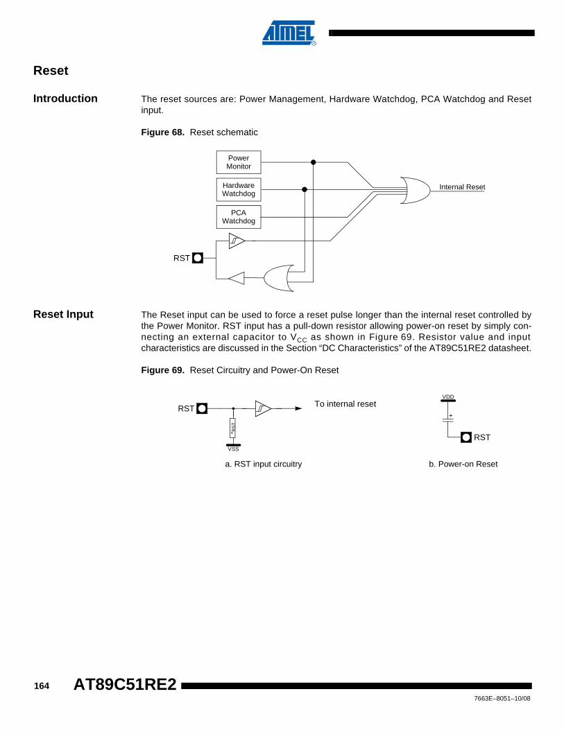
Reset
Introduction The reset sources are: Power Management, Hardware Watchdog, PCA Watchdog and Resetinput.
Figure 68. Reset schematic
Reset Input The Reset input can be used to force a reset pulse longer than the internal reset controlled bythe Power Monitor. RST input has a pull-down resistor allowing power-on reset by simply con-necting an external capacitor to VCC as shown in Figure 69. Resistor value and inputcharacteristics are discussed in the Section “DC Characteristics” of the AT89C51RE2 datasheet.
Figure 69. Reset Circuitry and Power-On Reset
PowerMonitor
HardwareWatchdog
PCAWatchdog
RST
Internal Reset
RST
RR
ST
VSS
To internal reset
RST
VDD
+
b. Power-on Reseta. RST input circuitry
1647663E–8051–10/08
AT89C51RE2
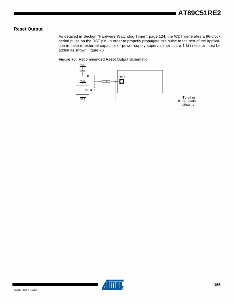
AT89C51RE2
Reset Output
As detailed in Section “Hardware Watchdog Timer”, page 124, the WDT generates a 96-clockperiod pulse on the RST pin. In order to properly propagate this pulse to the rest of the applica-tion in case of external capacitor or power-supply supervisor circuit, a 1 kΩ resistor must beadded as shown Figure 70.
Figure 70. Recommended Reset Output Schematic
RST
VDD
+
VSS
VDD
RST
1K
To otheron-boardcircuitry
1657663E–8051–10/08
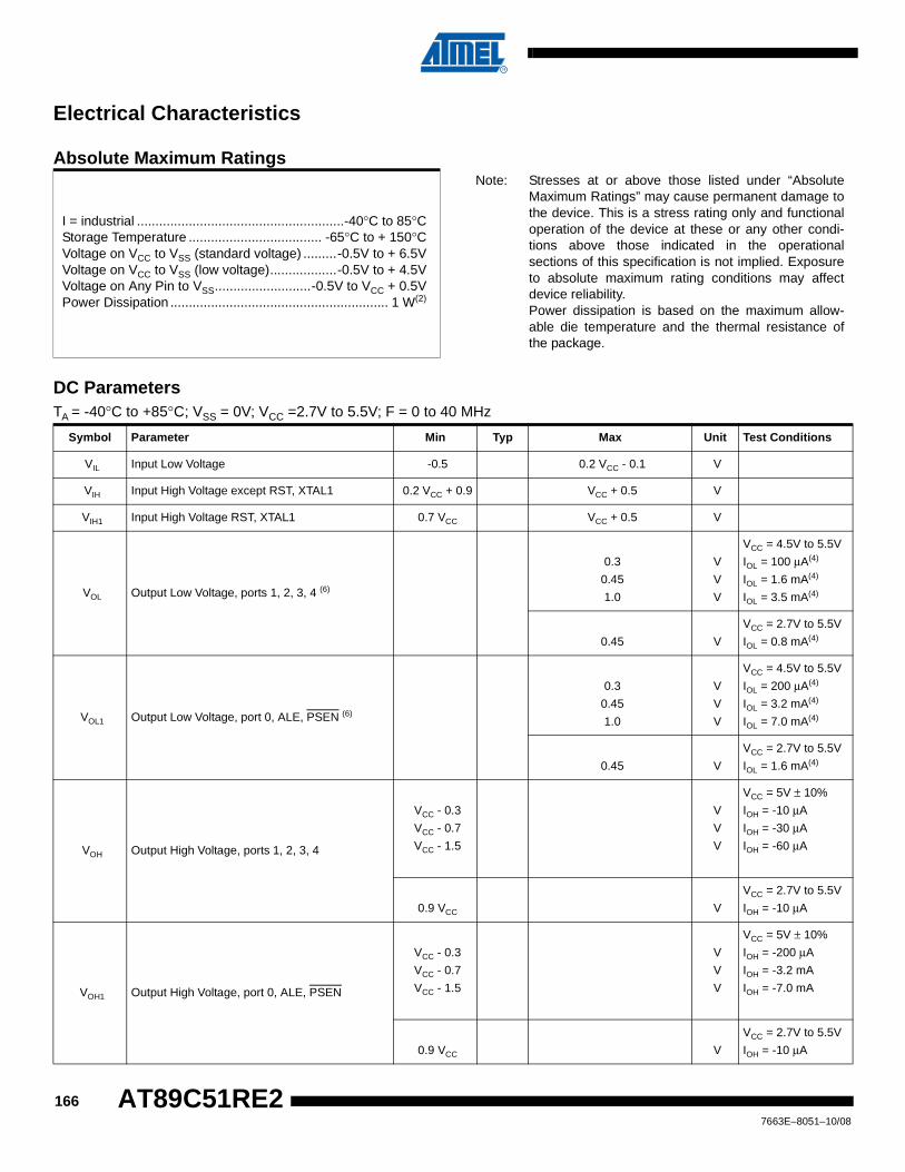
Electrical Characteristics
Absolute Maximum Ratings
DC Parameters
I = industrial ........................................................-40°C to 85°CStorage Temperature .................................... -65°C to + 150°CVoltage on VCC to VSS (standard voltage) .........-0.5V to + 6.5VVoltage on VCC to VSS (low voltage)..................-0.5V to + 4.5VVoltage on Any Pin to VSS..........................-0.5V to VCC + 0.5VPower Dissipation ........................................................... 1 W(2)
Note: Stresses at or above those listed under “AbsoluteMaximum Ratings” may cause permanent damage tothe device. This is a stress rating only and functionaloperation of the device at these or any other condi-tions above those indicated in the operationalsections of this specification is not implied. Exposureto absolute maximum rating conditions may affectdevice reliability.Power dissipation is based on the maximum allow-able die temperature and the thermal resistance ofthe package.
TA = -40°C to +85°C; VSS = 0V; VCC =2.7V to 5.5V; F = 0 to 40 MHz
Symbol Parameter Min Typ Max Unit Test Conditions
VIL Input Low Voltage -0.5 0.2 VCC - 0.1 V
VIH Input High Voltage except RST, XTAL1 0.2 VCC + 0.9 VCC + 0.5 V
VIH1 Input High Voltage RST, XTAL1 0.7 VCC VCC + 0.5 V
VOL Output Low Voltage, ports 1, 2, 3, 4 (6)
0.3
0.45
1.0
V
V
V
VCC = 4.5V to 5.5V
IOL = 100 μA(4)
IOL = 1.6 mA(4)
IOL = 3.5 mA(4)
0.45 V
VCC = 2.7V to 5.5V
IOL = 0.8 mA(4)
VOL1 Output Low Voltage, port 0, ALE, PSEN (6)
0.3
0.45
1.0
V
V
V
VCC = 4.5V to 5.5V
IOL = 200 μA(4)
IOL = 3.2 mA(4)
IOL = 7.0 mA(4)
0.45 V
VCC = 2.7V to 5.5V
IOL = 1.6 mA(4)
VOH Output High Voltage, ports 1, 2, 3, 4
VCC - 0.3
VCC - 0.7
VCC - 1.5
V
V
V
VCC = 5V ± 10%
IOH = -10 μA
IOH = -30 μA
IOH = -60 μA
0.9 VCC V
VCC = 2.7V to 5.5V
IOH = -10 μA
VOH1 Output High Voltage, port 0, ALE, PSEN
VCC - 0.3
VCC - 0.7
VCC - 1.5
V
V
V
VCC = 5V ± 10%
IOH = -200 μA
IOH = -3.2 mA
IOH = -7.0 mA
0.9 VCC V
VCC = 2.7V to 5.5V
IOH = -10 μA
1667663E–8051–10/08
AT89C51RE2
AT89C51RE2
Notes: 1. Operating ICC is measured with all output pins disconnected; XTAL1 driven with TCLCH, TCHCL = 5 ns (see Figure 74), VIL =VSS + 0.5V, VIH = VCC - 0.5V; XTAL2 N.C.; EA = RST = Port 0 = VCC. ICC would be slightly higher if a crystal oscillator used(see Figure 71).
2. Idle ICC is measured with all output pins disconnected; XTAL1 driven with TCLCH, TCHCL = 5 ns, VIL = VSS + 0.5V, VIH = VCC -0.5V; XTAL2 N.C; Port 0 = VCC; EA = RST = VSS (see Figure 72).
3. Power-down ICC is measured with all output pins disconnected; EA = VCC, PORT 0 = VCC; XTAL2 NC.; RST = VSS (see Fig-ure 73).
4. Capacitance loading on Ports 0 and 2 may cause spurious noise pulses to be superimposed on the VOLS of ALE and Ports 1and 3. The noise is due to external bus capacitance discharging into the Port 0 and Port 2 pins when these pins make 1 to 0transitions during bus operation. In the worst cases (capacitive loading 100 pF), the noise pulse on the ALE line may exceed0.45V with maxi VOL peak 0.6V. A Schmitt Trigger use is not necessary.
5. Typical values are based on a limited number of samples and are not guaranteed. The values listed are at room temperatureand 5V.
6. Under steady state (non-transient) conditions, IOL must be externally limited as follows:Maximum IOL per port pin: 10 mAMaximum IOL per 8-bit port:Port 0: 26 mAPorts 1, 2 and 3: 15 mAMaximum total IOL for all output pins: 71 mAIf IOL exceeds the test condition, VOL may exceed the related specification. Pins are not guaranteed to sink current greaterthan the listed test conditions.
Figure 71. ICC Test Condition, Active Mode
RRST RST Pull-down Resistor 50 200(5) 250 kΩ
IIL Logical 0 Input Current ports 1, 2, 3, 4 and 5 -50 μA VIN = 0.45V
ILI Input Leakage Current ±10 μA 0.45V < VIN < VCC
ITL Logical 1 to 0 Transition Current, ports 1, 2, 3, 4 -650 μA VIN = 2.0V
CIO Capacitance of I/O Buffer 10 pFFC = 3 MHzTA = 25°C
IPD Power-down Current 75 150 μA 2.7 < VCC < 5.5V(3)
ICCOP Power Supply Current on normal mode 0.4 x Frequency (MHz) + 5 mA VCC = 5.5V(1)
ICCIDLE Power Supply Current on idle mode 0.3 x Frequency (MHz) + 5 mA VCC = 5.5V(2)
ICCWRITE Power Supply Current on flash write 0.8 x Frequency (MHz) + 15 mA VCC = 5.5V
tWRITE Flash programming time 7 10 ms 2.7 < VCC < 5.5V
TA = -40°C to +85°C; VSS = 0V; VCC =2.7V to 5.5V; F = 0 to 40 MHz (Continued)
Symbol Parameter Min Typ Max Unit Test Conditions
EA
VCC
VCC
ICC
(NC)CLOCK SIGNAL
VCC
All other pins are disconnected.
RST
XTAL2XTAL1
VSS
VCC
P0
1677663E–8051–10/08
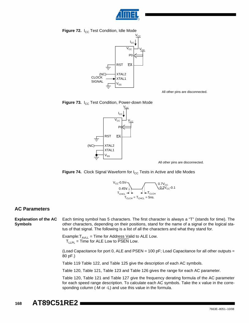
Figure 72. ICC Test Condition, Idle Mode
Figure 73. ICC Test Condition, Power-down Mode
Figure 74. Clock Signal Waveform for ICC Tests in Active and Idle Modes
AC Parameters
Explanation of the AC Symbols
Each timing symbol has 5 characters. The first character is always a “T” (stands for time). Theother characters, depending on their positions, stand for the name of a signal or the logical sta-tus of that signal. The following is a list of all the characters and what they stand for.
Example:TAVLL = Time for Address Valid to ALE Low.TLLPL = Time for ALE Low to PSEN Low.
(Load Capacitance for port 0, ALE and PSEN = 100 pF; Load Capacitance for all other outputs =80 pF.)
Table 119 Table 122, and Table 125 give the description of each AC symbols.
Table 120, Table 121, Table 123 and Table 126 gives the range for each AC parameter.
Table 120, Table 121 and Table 127 give the frequency derating formula of the AC parameterfor each speed range description. To calculate each AC symbols. Take the x value in the corre-sponding column (-M or -L) and use this value in the formula.
RST EA
XTAL2XTAL1
VSS
VCC
VCC
ICC
(NC)
P0
VCC
All other pins are disconnected.
CLOCK SIGNAL
RST EA
XTAL2XTAL1
VSS
VCC
VCC
ICC
(NC)
P0
VCC
All other pins are disconnected.
VCC-0.5V
0.45V
0.7VCC0.2VCC-0.1
TCLCHTCHCL
TCLCH = TCHCL = 5ns.
1687663E–8051–10/08
AT89C51RE2
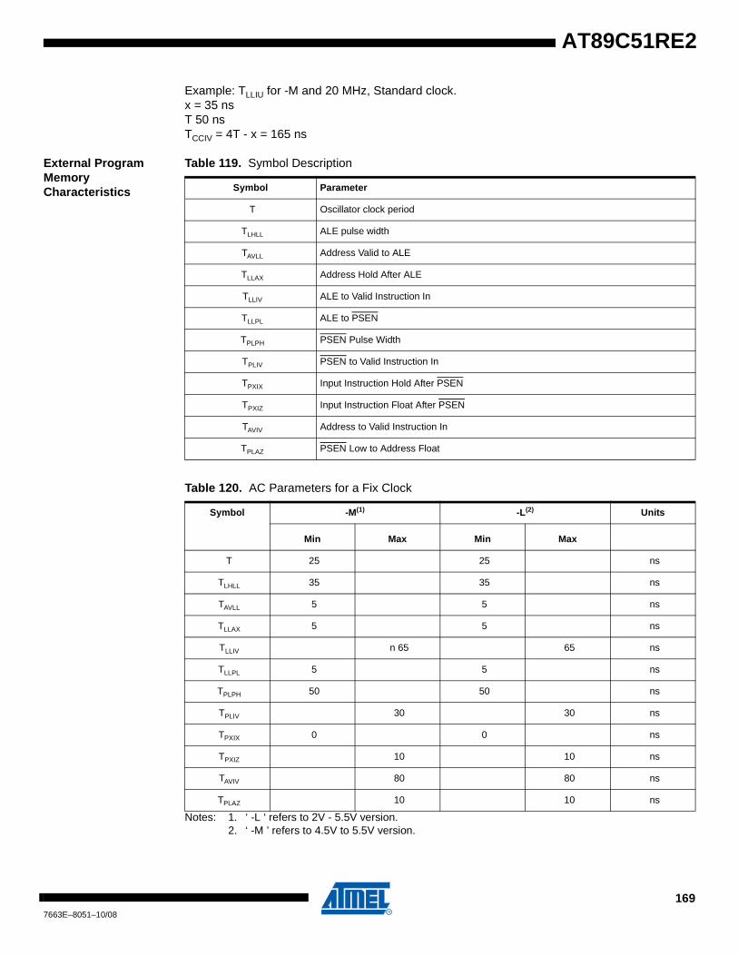
AT89C51RE2
Example: TLLIU for -M and 20 MHz, Standard clock.x = 35 nsT 50 nsTCCIV = 4T - x = 165 ns
External Program Memory Characteristics
Table 119. Symbol Description
Table 120. AC Parameters for a Fix Clock
Notes: 1. ‘ -L ‘ refers to 2V - 5.5V version.2. ‘ -M ’ refers to 4.5V to 5.5V version.
Symbol Parameter
T Oscillator clock period
TLHLL ALE pulse width
TAVLL Address Valid to ALE
TLLAX Address Hold After ALE
TLLIV ALE to Valid Instruction In
TLLPL ALE to PSEN
TPLPH PSEN Pulse Width
TPLIV PSEN to Valid Instruction In
TPXIX Input Instruction Hold After PSEN
TPXIZ Input Instruction Float After PSEN
TAVIV Address to Valid Instruction In
TPLAZ PSEN Low to Address Float
Symbol -M(1) -L(2) Units
Min Max Min Max
T 25 25 ns
TLHLL 35 35 ns
TAVLL 5 5 ns
TLLAX 5 5 ns
TLLIV n 65 65 ns
TLLPL 5 5 ns
TPLPH 50 50 ns
TPLIV 30 30 ns
TPXIX 0 0 ns
TPXIZ 10 10 ns
TAVIV 80 80 ns
TPLAZ 10 10 ns
1697663E–8051–10/08
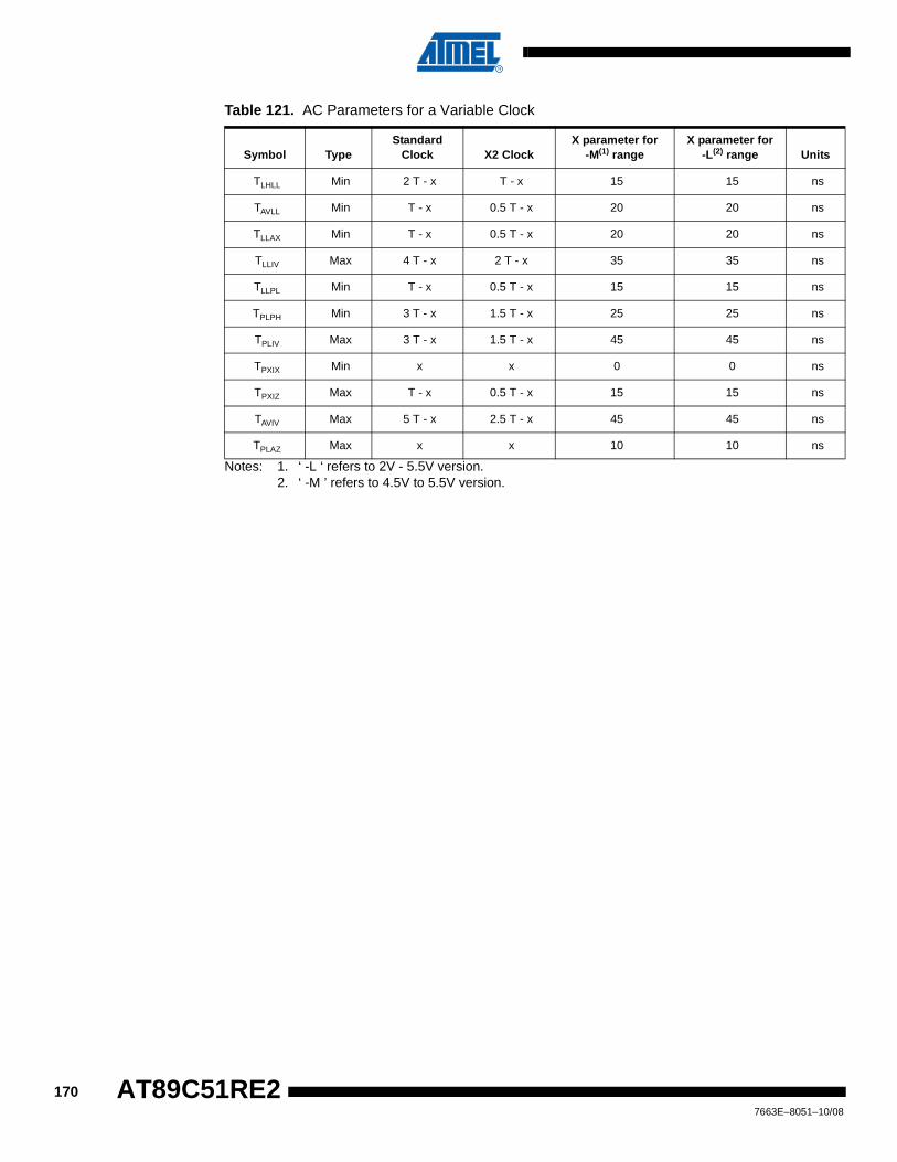
Table 121. AC Parameters for a Variable Clock
Notes: 1. ‘ -L ‘ refers to 2V - 5.5V version.2. ‘ -M ’ refers to 4.5V to 5.5V version.
Symbol TypeStandard
Clock X2 Clock X parameter for
-M(1) rangeX parameter for
-L(2) range Units
TLHLL Min 2 T - x T - x 15 15 ns
TAVLL Min T - x 0.5 T - x 20 20 ns
TLLAX Min T - x 0.5 T - x 20 20 ns
TLLIV Max 4 T - x 2 T - x 35 35 ns
TLLPL Min T - x 0.5 T - x 15 15 ns
TPLPH Min 3 T - x 1.5 T - x 25 25 ns
TPLIV Max 3 T - x 1.5 T - x 45 45 ns
TPXIX Min x x 0 0 ns
TPXIZ Max T - x 0.5 T - x 15 15 ns
TAVIV Max 5 T - x 2.5 T - x 45 45 ns
TPLAZ Max x x 10 10 ns
1707663E–8051–10/08
AT89C51RE2
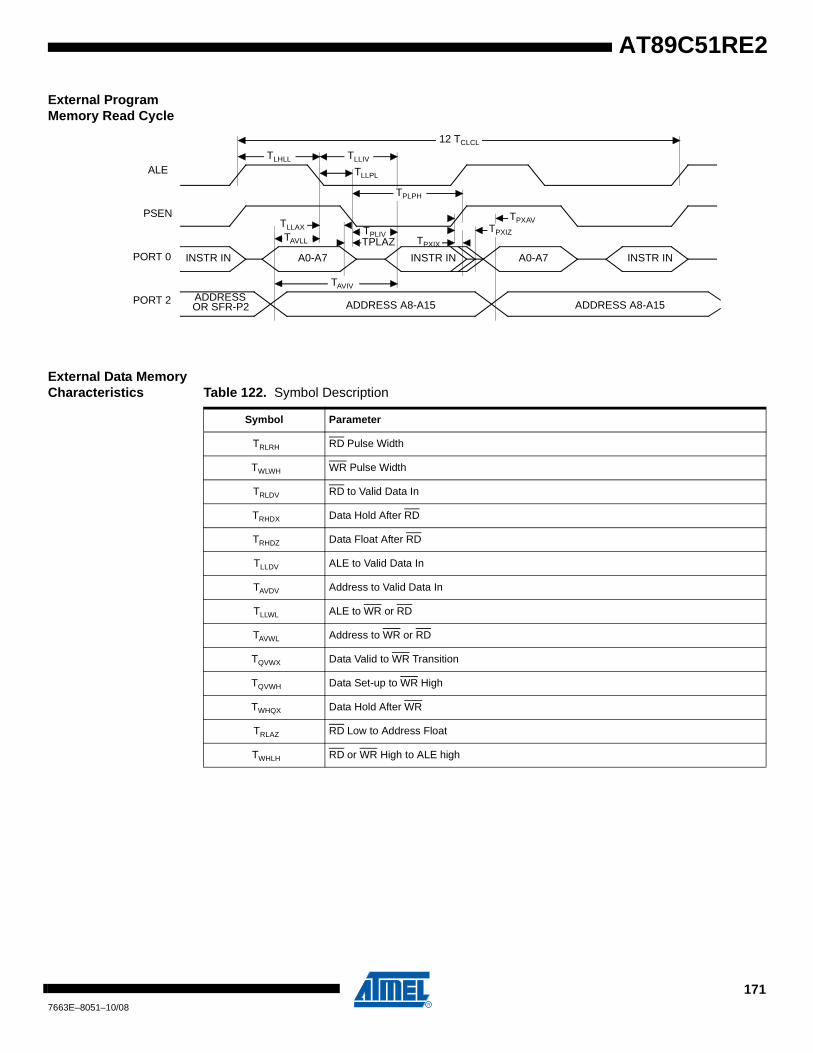
AT89C51RE2
External Program Memory Read Cycle
External Data Memory Characteristics Table 122. Symbol Description
TPLIVTPLAZ
ALE
PSEN
PORT 0
PORT 2
A0-A7A0-A7 INSTR ININSTR IN INSTR IN
ADDRESSOR SFR-P2 ADDRESS A8-A15ADDRESS A8-A15
12 TCLCL
TAVIV
TLHLL
TAVLL
TLLIV
TLLPL
TPLPH
TPXAV
TPXIX
TPXIZTLLAX
Symbol Parameter
TRLRH RD Pulse Width
TWLWH WR Pulse Width
TRLDV RD to Valid Data In
TRHDX Data Hold After RD
TRHDZ Data Float After RD
TLLDV ALE to Valid Data In
TAVDV Address to Valid Data In
TLLWL ALE to WR or RD
TAVWL Address to WR or RD
TQVWX Data Valid to WR Transition
TQVWH Data Set-up to WR High
TWHQX Data Hold After WR
TRLAZ RD Low to Address Float
TWHLH RD or WR High to ALE high
1717663E–8051–10/08

Table 123. AC Parameters for a Fix Clock
Notes: 1. ‘ -L ‘ refers to 2V - 5.5V version.2. ‘ -M ’ refers to 4.5V to 5.5V version.
Symbol
-M(1) -L(2)
UnitsMin Max Min Max
TRLRH 125 125 ns
TWLWH 125 125 ns
TRLDV 95 95 ns
TRHDX 0 0 ns
TRHDZ 25 25 ns
TLLDV 155 155 ns
TAVDV 160 160 ns
TLLWL 45 105 45 105 ns
TAVWL 70 70 ns
TQVWX 5 5 ns
TQVWH 155 155 ns
TWHQX 10 10 ns
TRLAZ 0 0 ns
TWHLH 5 45 5 45 ns
1727663E–8051–10/08
AT89C51RE2
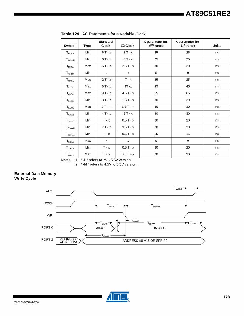
AT89C51RE2
Notes: 1. ‘ -L ‘ refers to 2V - 5.5V version.2. ‘ -M ’ refers to 4.5V to 5.5V version.
External Data Memory Write Cycle
Table 124. AC Parameters for a Variable Clock
Symbol TypeStandard
Clock X2 ClockX parameter for
-M(1) rangeX parameter for
-L(2) range Units
TRLRH Min 6 T - x 3 T - x 25 25 ns
TWLWH Min 6 T - x 3 T - x 25 25 ns
TRLDV Max 5 T - x 2.5 T - x 30 30 ns
TRHDX Min x x 0 0 ns
TRHDZ Max 2 T - x T - x 25 25 ns
TLLDV Max 8 T - x 4T -x 45 45 ns
TAVDV Max 9 T - x 4.5 T - x 65 65 ns
TLLWL Min 3 T - x 1.5 T - x 30 30 ns
TLLWL Max 3 T + x 1.5 T + x 30 30 ns
TAVWL Min 4 T - x 2 T - x 30 30 ns
TQVWX Min T - x 0.5 T - x 20 20 ns
TQVWH Min 7 T - x 3.5 T - x 20 20 ns
TWHQX Min T - x 0.5 T - x 15 15 ns
TRLAZ Max x x 0 0 ns
TWHLH Min T - x 0.5 T - x 20 20 ns
TWHLH Max T + x 0.5 T + x 20 20 ns
TQVWHTLLAX
ALE
PSEN
WR
PORT 0
PORT 2
A0-A7 DATA OUT
ADDRESSOR SFR-P2
TAVWL
TLLWL
TQVWX
ADDRESS A8-A15 OR SFR P2
TWHQX
TWHLH
TWLWH
1737663E–8051–10/08
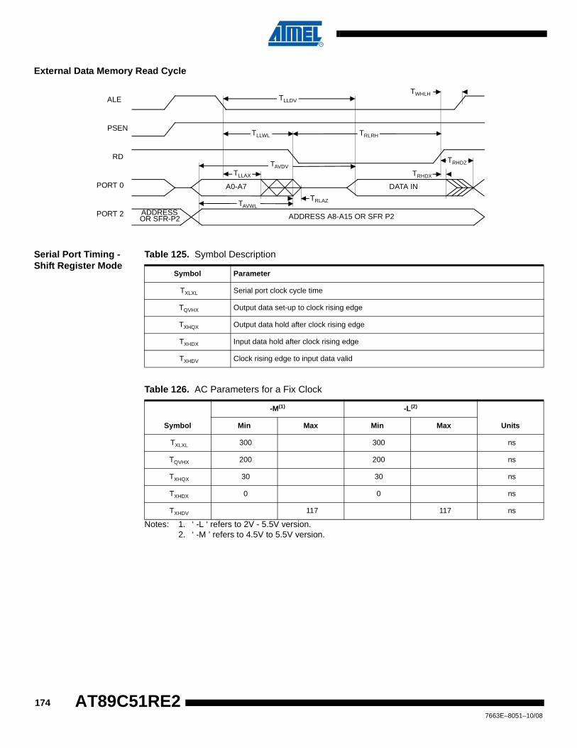
External Data Memory Read Cycle
Serial Port Timing - Shift Register Mode
Table 125. Symbol Description
Table 126. AC Parameters for a Fix Clock
Notes: 1. ‘ -L ‘ refers to 2V - 5.5V version.2. ‘ -M ’ refers to 4.5V to 5.5V version.
ALE
PSEN
RD
PORT 0
PORT 2
A0-A7 DATA IN
ADDRESSOR SFR-P2
TAVWL
TLLWL
TRLAZ
ADDRESS A8-A15 OR SFR P2
TRHDZ
TWHLH
TRLRH
TLLDV
TRHDXTLLAX
TAVDV
Symbol Parameter
TXLXL Serial port clock cycle time
TQVHX Output data set-up to clock rising edge
TXHQX Output data hold after clock rising edge
TXHDX Input data hold after clock rising edge
TXHDV Clock rising edge to input data valid
Symbol
-M(1) -L(2)
UnitsMin Max Min Max
TXLXL 300 300 ns
TQVHX 200 200 ns
TXHQX 30 30 ns
TXHDX 0 0 ns
TXHDV 117 117 ns
1747663E–8051–10/08
AT89C51RE2
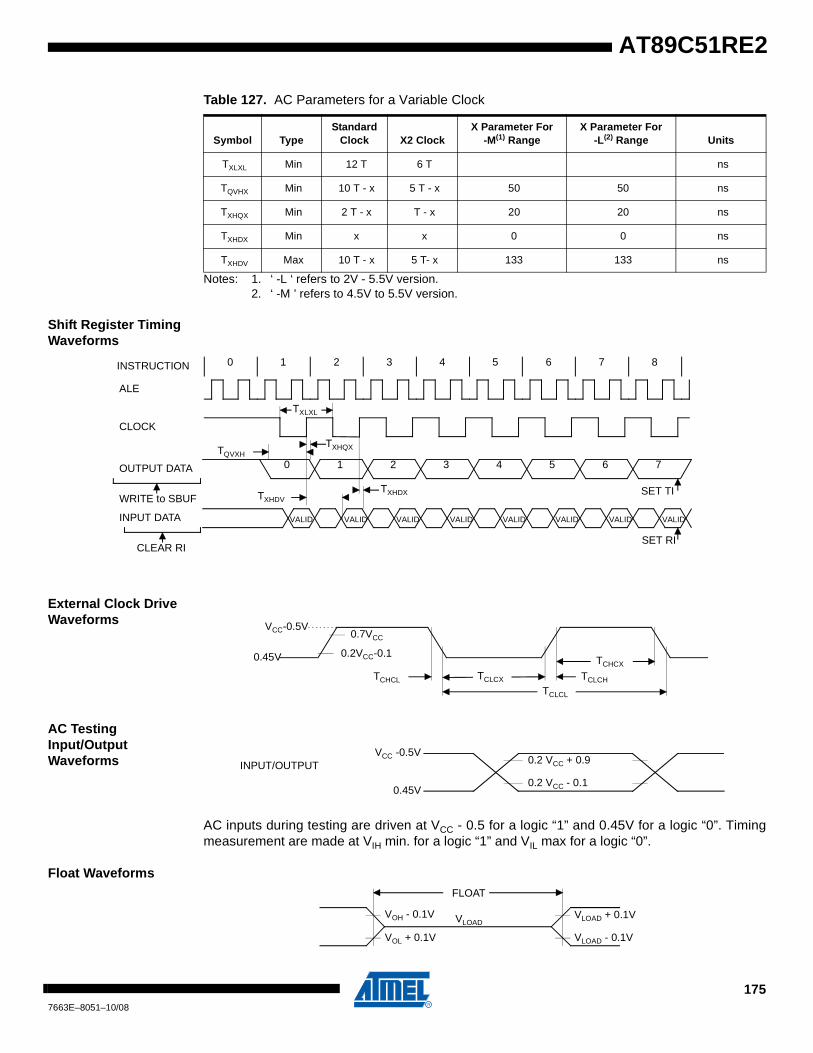
AT89C51RE2
Table 127. AC Parameters for a Variable Clock
Notes: 1. ‘ -L ‘ refers to 2V - 5.5V version.2. ‘ -M ’ refers to 4.5V to 5.5V version.
Shift Register Timing Waveforms
External Clock Drive Waveforms
AC Testing Input/Output Waveforms
AC inputs during testing are driven at VCC - 0.5 for a logic “1” and 0.45V for a logic “0”. Timingmeasurement are made at VIH min. for a logic “1” and VIL max for a logic “0”.
Float Waveforms
Symbol TypeStandard
Clock X2 ClockX Parameter For
-M(1) RangeX Parameter For
-L(2) Range Units
TXLXL Min 12 T 6 T ns
TQVHX Min 10 T - x 5 T - x 50 50 ns
TXHQX Min 2 T - x T - x 20 20 ns
TXHDX Min x x 0 0 ns
TXHDV Max 10 T - x 5 T- x 133 133 ns
INPUT DATA VALIDVALID VALID VALID
0 1 2 3 4 5 6 87
ALE
CLOCK
OUTPUT DATA
WRITE to SBUF
CLEAR RI
TXLXL
TQVXHTXHQX
TXHDVTXHDX SET TI
SET RI
INSTRUCTION
0 1 2 3 4 5 6 7
VALID VALID VALID VALID
VCC-0.5V
0.45V
0.7VCC
0.2VCC-0.1
TCHCL TCLCX
TCLCL
TCLCH
TCHCX
INPUT/OUTPUT 0.2 VCC + 0.9
0.2 VCC - 0.1
VCC -0.5V
0.45V
FLOAT
VOH - 0.1V
VOL + 0.1V
VLOADVLOAD + 0.1V
VLOAD - 0.1V
1757663E–8051–10/08
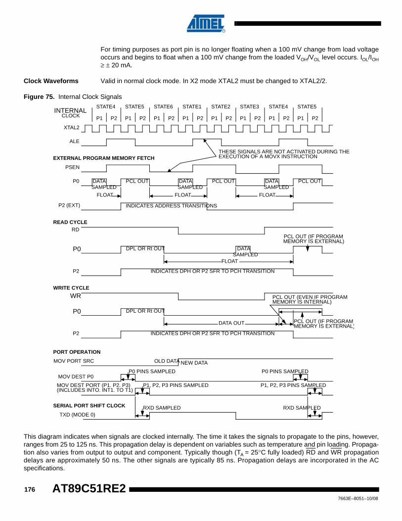
For timing purposes as port pin is no longer floating when a 100 mV change from load voltageoccurs and begins to float when a 100 mV change from the loaded VOH/VOL level occurs. IOL/IOH≥ ± 20 mA.
Clock Waveforms Valid in normal clock mode. In X2 mode XTAL2 must be changed to XTAL2/2.
Figure 75. Internal Clock Signals
This diagram indicates when signals are clocked internally. The time it takes the signals to propagate to the pins, however,ranges from 25 to 125 ns. This propagation delay is dependent on variables such as temperature and pin loading. Propaga-tion also varies from output to output and component. Typically though (TA = 25°C fully loaded) RD and WR propagationdelays are approximately 50 ns. The other signals are typically 85 ns. Propagation delays are incorporated in the ACspecifications.
DATA PCL OUT DATA PCL OUT DATA PCL OUT SAMPLED SAMPLED SAMPLED
STATE4 STATE5 STATE6 STATE1 STATE2 STATE3 STATE4 STATE5
P1 P2 P1 P2 P1 P2 P1 P2 P1 P2 P1 P2 P1 P2 P1 P2
FLOAT FLOAT FLOAT
THESE SIGNALS ARE NOT ACTIVATED DURING THEEXECUTION OF A MOVX INSTRUCTION
INDICATES ADDRESS TRANSITIONS
EXTERNAL PROGRAM MEMORY FETCH
FLOAT
DATASAMPLED
DPL OR Rt OUT
INDICATES DPH OR P2 SFR TO PCH TRANSITION
PCL OUT (IF PROGRAMMEMORY IS EXTERNAL)
PCL OUT (EVEN IF PROGRAMMEMORY IS INTERNAL)
PCL OUT (IF PROGRAMMEMORY IS EXTERNAL)
OLD DATA NEW DATA
P0 PINS SAMPLED
P1, P2, P3 PINS SAMPLED P1, P2, P3 PINS SAMPLED
P0 PINS SAMPLED
RXD SAMPLED
INTERNALCLOCK
XTAL2
ALE
PSEN
P0
P2 (EXT)
READ CYCLE
WRITE CYCLE
RD
P0
P2
WR
PORT OPERATION
MOV PORT SRC
MOV DEST P0
MOV DEST PORT (P1. P2. P3)(INCLUDES INTO. INT1. TO T1)
SERIAL PORT SHIFT CLOCK
TXD (MODE 0)
DATA OUT
DPL OR Rt OUT
INDICATES DPH OR P2 SFR TO PCH TRANSITION
P0
P2
RXD SAMPLED
1767663E–8051–10/08
AT89C51RE2
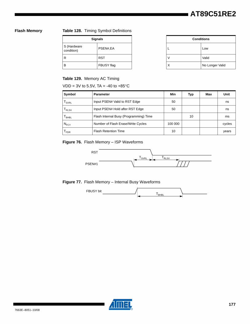
AT89C51RE2
Flash Memory Table 128. Timing Symbol Definitions
Table 129. Memory AC Timing
VDD = 3V to 5.5V, TA = -40 to +85°C
Figure 76. Flash Memory – ISP Waveforms
Figure 77. Flash Memory – Internal Busy Waveforms
Signals Conditions
S (Hardware condition)
PSEN#,EA L Low
R RST V Valid
B FBUSY flag X No Longer Valid
Symbol Parameter Min Typ Max Unit
TSVRL Input PSEN# Valid to RST Edge 50 ns
TRLSX Input PSEN# Hold after RST Edge 50 ns
TBHBL Flash Internal Busy (Programming) Time 10 ms
NFCY Number of Flash Erase/Write Cycles 100 000 cycles
TFDR Flash Retention Time 10 years
RST
TSVRL
PSEN#1
TRLSX
FBUSY bitTBHBL
1777663E–8051–10/08
Ordering Information
Table 130. Possible Order Entries
Part Number Supply Voltage Temperature Range Package
AT89C51RE2-SLSUM2.7V-5.5V Industrial & Green
PLCC44
AT89C51RE2-RLTUM VQFP44
AT89C51RE2-SLSEM2.7V-5.5V Engineering Samples
PLCC44
AT89C51RE2-RLTEM VQFP44
1787663E–8051–10/08
AT89C51RE2

AT89C51RE2
Packaging Information
PLCC44
1797663E–8051–10/08
STANDARD NOTES FOR PLCC
1/ CONTROLLING DIMENSIONS : INCHES
2/ DIMENSIONING AND TOLERANCING PER ANSI Y 14.5M - 1982.
3/ "D" AND "E1" DIMENSIONS DO NOT INCLUDE MOLD FLASH OR PROTUSIONS.MOLD FLASH OR PROTUSIONS SHALL NOT EXCEED 0.20 mm (.008 INCH) PER
SIDE.
1807663E–8051–10/08
AT89C51RE2
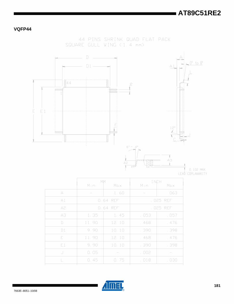
AT89C51RE2
VQFP44
1817663E–8051–10/08
STANDARD NOTES FOR PQFP/ VQFP / TQFP / DQFP
1/ CONTROLLING DIMENSIONS : INCHES
2/ ALL DIMENSIONING AND TOLERANCING CONFORM TO ANSI Y 14.5M -1982.
3/ "D1 AND E1" DIMENSIONS DO NOT INCLUDE MOLD PROTUSIONS.
MOLD PROTUSIONS SHALL NOT EXCEED 0.25 mm (0.010 INCH).
THE TOP PACKAGE BODY SIZE MAY BE SMALLER THAN THE BOTTOM
PACKAGE BODY SIZE BY AS MUCH AS 0.15 mm.
4/ DATUM PLANE "H" LOCATED AT MOLD PARTING LINE AND
COINCIDENT WITH LEAD, WHERE LEAD EXITS PLASTIC BODY AT
BOTTOM OF PARTING LINE.
5/ DATUM "A" AND "D" TO BE DETERMINED AT DATUM PLANE H.
6/ DIMENSION " f " DOES NOT INCLUDE DAMBAR PROTUSION ALLOWABLE
DAMBAR PROTUSION SHALL BE 0.08mm/.003" TOTAL IN EXCESS OF THE
" f " DIMENSION AT MAXIMUM MATERIAL CONDITION .
DAMBAR CANNOT BE LOCATED ON THE LOWER RADIUS OR THE FOOT.
1827663E–8051–10/08
AT89C51RE2
AT89C51RE2
Document Revision History
Changes from 7663B to 7663C
1. Modified ordering information.
2. Various grammatical corections throughout document.
Changes from 7663C to 7663D
1. TWI interface added.
Changes from 7663D to 7663E
1. Removed 64 and 68 pins package product version.
2. Minor correction on Table 69 on page 102.
1837663E–8051–10/08
Features ................................................................................................. 1
Description ............................................................................................ 2
Block Diagram ...................................................................................... 3
Pin Configurations ............................................................................... 4
SFR Mapping ......................................................................................... 7
Enhanced Features ............................................................................ 13X2 Feature .......................................................................................................... 13
Dual Data Pointer Register DPTR ..................................................... 18Memory Architecture ...........................................................................................21
Expanded RAM (XRAM) ..................................................................... 22Registers............................................................................................................. 24Extended Stack................................................................................................... 25
Flash Memory ..................................................................................... 27General Description ............................................................................................ 27Features.............................................................................................................. 27Flash memory organization ................................................................................ 27On-Chip Flash memory....................................................................................... 28On-Chip ROM bootloader ................................................................................... 31Boot process....................................................................................................... 32Access and Operations Descriptions.................................................................. 36
Operation Cross Memory Access ..................................................... 50
Sharing Instructions ........................................................................... 50
Flash Protection from Parallel Programming .................................. 52
Bootloader Architecture .................................................................... 53Introduction ......................................................................................................... 53Bootloader Description ....................................................................................... 54ISP Protocol Description..................................................................................... 56Protocol............................................................................................................... 57ISP Commands description ................................................................................ 61
Timers/Counters ................................................................................. 68Timer/Counter Operations .................................................................................. 68Timer 0................................................................................................................ 68Timer 1................................................................................................................ 71
17663E–8051–10/08
AT89C51RE2
AT89C51RE2
Interrupt .............................................................................................................. 71Registers............................................................................................................. 73
Timer 2 ................................................................................................. 77Auto-Reload Mode.............................................................................................. 77Programmable Clock-Output .............................................................................. 78Registers............................................................................................................. 80
Programmable Counter Array PCA ................................................... 82PCA Capture Mode............................................................................................. 9016-bit Software Timer/ Compare Mode............................................................... 90High Speed Output Mode ................................................................................... 91Pulse Width Modulator Mode.............................................................................. 92PCA Watchdog Timer ......................................................................................... 93
Serial I/O Port ...................................................................................... 94Framing Error Detection ..................................................................................... 94Automatic Address Recognition.......................................................................... 95Registers............................................................................................................. 97Baud Rate Selection for UART 0 for Mode 1 and 3............................................ 98Baud Rate Selection for UART 1 for Mode 1 and 3............................................ 99UART Registers................................................................................................ 103
Interrupt System ............................................................................... 109Registers........................................................................................................... 110Interrupt Sources and Vector Addresses.......................................................... 117
Power Management .......................................................................... 118Introduction ....................................................................................................... 118Idle Mode.......................................................................................................... 118Power-Down Mode ........................................................................................... 118Registers........................................................................................................... 121
Oscillator ........................................................................................... 122Registers........................................................................................................... 122Functional Block Diagram .................................................................................123
Hardware Watchdog Timer .............................................................. 124Using the WDT ................................................................................................. 124WDT During Power Down and Idle................................................................... 125
Reduced EMI Mode ........................................................................... 126
Keyboard Interface ........................................................................... 127Registers........................................................................................................... 128
27663E–8051–10/08

2-wire Interface (TWI) ....................................................................... 131Description........................................................................................................ 133Notes ................................................................................................................ 136Registers........................................................................................................... 146
Serial Port Interface (SPI) ................................................................ 149Features............................................................................................................ 149Signal Description............................................................................................. 149Functional Description ...................................................................................... 151
Power Monitor ................................................................................... 161Description........................................................................................................ 161
Power-off Flag ................................................................................... 163
Reset .................................................................................................. 164Introduction ....................................................................................................... 164Reset Input ....................................................................................................... 164Reset Output .....................................................................................................165
Electrical Characteristics ................................................................. 166Absolute Maximum Ratings ..............................................................................166DC Parameters .................................................................................................166AC Parameters ................................................................................................. 168
Ordering Information ........................................................................ 178
Packaging Information ..................................................................... 179PLCC44 ............................................................................................................ 179VQFP44............................................................................................................ 181
Document Revision History ............................................................. 183Changes from 7663B to 7663C ........................................................................ 183Changes from 7663C to 7663D........................................................................ 183Changes from 7663D to 7663E ........................................................................ 183
37663E–8051–10/08
AT89C51RE2
Headquarters International
Atmel Corporation2325 Orchard ParkwaySan Jose, CA 95131USATel: 1(408) 441-0311Fax: 1(408) 487-2600
Atmel AsiaRoom 1219Chinachem Golden Plaza77 Mody Road TsimshatsuiEast KowloonHong KongTel: (852) 2721-9778Fax: (852) 2722-1369
Atmel EuropeLe Krebs8, Rue Jean-Pierre TimbaudBP 30978054 Saint-Quentin-en-Yvelines CedexFranceTel: (33) 1-30-60-70-00 Fax: (33) 1-30-60-71-11
Atmel Japan9F, Tonetsu Shinkawa Bldg.1-24-8 ShinkawaChuo-ku, Tokyo 104-0033JapanTel: (81) 3-3523-3551Fax: (81) 3-3523-7581
Product Contact
Web Sitewww.atmel.com
Technical [email protected]
Sales Contactwww.atmel.com/contacts
Literature Requestswww.atmel.com/literature
Disclaimer: The information in this document is provided in connection with Atmel products. No license, express or implied, by estoppel or otherwise, to anyintellectual property right is granted by this document or in connection with the sale of Atmel products. EXCEPT AS SET FORTH IN ATMEL’S TERMS AND CONDI-TIONS OF SALE LOCATED ON ATMEL’S WEB SITE, ATMEL ASSUMES NO LIABILITY WHATSOEVER AND DISCLAIMS ANY EXPRESS, IMPLIED OR STATUTORYWARRANTY RELATING TO ITS PRODUCTS INCLUDING, BUT NOT LIMITED TO, THE IMPLIED WARRANTY OF MERCHANTABILITY, FITNESS FOR A PARTICULARPURPOSE, OR NON-INFRINGEMENT. IN NO EVENT SHALL ATMEL BE LIABLE FOR ANY DIRECT, INDIRECT, CONSEQUENTIAL, PUNITIVE, SPECIAL OR INCIDEN-TAL DAMAGES (INCLUDING, WITHOUT LIMITATION, DAMAGES FOR LOSS OF PROFITS, BUSINESS INTERRUPTION, OR LOSS OF INFORMATION) ARISING OUTOF THE USE OR INABILITY TO USE THIS DOCUMENT, EVEN IF ATMEL HAS BEEN ADVISED OF THE POSSIBILITY OF SUCH DAMAGES. Atmel makes norepresentations or warranties with respect to the accuracy or completeness of the contents of this document and reserves the right to make changes to specificationsand product descriptions at any time without notice. Atmel does not make any commitment to update the information contained herein. Unless specifically providedotherwise, Atmel products are not suitable for, and shall not be used in, automotive applications. Atmel’s products are not intended, authorized, or warranted for useas components in applications intended to support or sustain life.
© 2008 Atmel Corporation. All rights reserved. Atmel®, logo and combinations thereof, and others are registered trademarks or trademarks ofAtmel Corporation or its subsidiaries. Other terms and product names may be trademarks of others.
7663E–8051–10/08
Recommended
![AT24C256C - ww1.microchip.comww1.microchip.com/downloads/en/DeviceDoc/Atmel-8568-SEEPROM-AT24C25… · AT24C256C [DATASHEET] Atmel-8568F-SEEPROM-AT24C256C-Datasheet_012015 6 6. Device](https://img.pdfslide.us/doc/110x75/5e19dbf9d55cfc7fce018509/at24c256c-ww1-at24c256c-datasheet-atmel-8568f-seeprom-at24c256c-datasheet012015.jpg)