Embed Size (px)
Citation preview

MIC2026A/2076A
Dual-Channel Power Distribution Switch
Micrel Inc. • 2180 Fortune Drive • San Jose, CA 95131 • USA • tel +1 (408) 944-0800 • fax + 1 (408) 474-1000 • http://www.micrel.com
July 2009
M9999-072309-B(408) 955-1690
General Description The MIC2026A and MIC2076A are high-side MOSFET switches optimized for general-purpose power distribution requiring circuit protection. The MIC2026A is particularly well suited for USB applications. The MIC2026A/2076A are internally current limited and have thermal shutdown that protects the device and load. The MIC2076A offers “smart” shutdown that reduces current consumption in fault modes. When the MIC2076A goes into thermal shutdown due to current limiting, the output is latched off until the switch is reset. The MIC2076A can be reset by removing the load, toggling the enable input, or cycling VIN. Both devices employ soft-start circuitry that minimizes inrush current in applications where highly capacitive loads are employed. A fault status output flag is asserted during overcurrent or thermal shutdown conditions. Transient faults are internally filtered. The MIC2026A/2076A are available in an 8-pin SOIC package. All support documentation can be found on Micrel’s web site at www.micrel.com.
Features • 100mΩ typical RDS(ON) at 5.0V • 140mΩ maximum RDS(ON) at 5.0V • 2.7 V to 5.5 V operating range • 500mA minimum continuous current per channel • Short circuit protection with thermal shutdown • Thermally isolated channels • Soft-start circuit • Fault status flag with 3ms filter eliminates false
assertions • UVLO (Undervoltage lockout) • Reverse current flow blocking (no “body diode”) • Circuit breaker mode (MIC2076A) • Pin compatible with the MIC2026/2076 • Logic-compatible inputs • Low quiescent current
Applications • USB peripherals • General purpose power switching • ACPI power distribution • Notebook PCs • PDAs • PC card hot swap
_______________________________________________________________________________________________
Typical Application
Micrel, Inc. MIC2026A/2076A
July 2009 2 M9999-072309-B(408) 955-1690
Ordering Information Part Number Enable Temperature Range Package Lead Finish MIC2026A-1YM Active High –40° to +85°C 8- Pin SOIC Pb-Free MIC2026A-2YM Active Low –40° to +85°C 8- Pin SOIC Pb-Free MIC2076A-1YM Active High –40° to +85°C 8- Pin SOIC Pb-Free MIC2076A-2YM Active Low –40° to +85°C 8- Pin SOIC Pb-Free
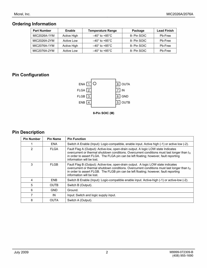
Pin Configuration
1ENA
FLGA
FLGB
ENB
8 OUTA
IN
GND
OUTB
7
6
5
2
3
4
8-Pin SOIC (M)
Pin Description
Pin Number Pin Name Pin Function 1 ENA Switch A Enable (Input): Logic-compatible, enable input. Active high (-1) or active low (-2). 2 FLGA Fault Flag A (Output): Active-low, open-drain output. A logic LOW state Indicates
overcurrent or thermal shutdown conditions. Overcurrent conditions must last longer than tBDB in order to assert FLGA. The FLGA pin can be left floating; however, fault reporting information will be lost.
3 FLGB Fault Flag B (Output): Active-low, open-drain output. A logic LOW state indicates overcurrent or thermal shutdown conditions. Overcurrent conditions must last longer than tBDB in order to assert FLGB. The FLGB pin can be left floating; however, fault reporting information will be lost.
4 ENB Switch B Enable (Input): Logic-compatible enable input. Active-high (-1) or active-low (-2). 5 OUTB Switch B (Output). 6 GND Ground. 7 IN Input: Switch and logic supply input. 8 OUTA Switch A (Output).

Micrel, Inc. MIC2026A/2076A
July 2009 3 M9999-072309-B(408) 955-1690
Absolute Maximum RatingsP
(1)
Supply Voltage (VIN) ....................................... –0.3V to +6V Output Voltage (OUTA and OUTB) ................ –0.3V to +6V All other pins voltages ..................................... –0.3V to +6V Fault Flag Current (IBFLGB)..............................................25mA Output Current (IBOUTB)................................. Internally Limited Storage Temperature (TBSB) .......................–65°C to +150 °C ESD Rating(3) HBM......................................................................... 3kV MM.........................................................................200V Lead Temperature (Soldering 10 sec) ....................... 260°C
Operating RatingsP
(2)
Supply Voltage (VBINB) .................................... +2.7V to +5.5V Ambient Temperature (TBAB)..........................–40°C to +85°C Junction Temperature Range (TBJB) ............ Internally Limited Thermal Resistance SOIC (θBJAB) .......................................................160°C/W
Electrical Characteristics(4)
VIN = 5V; TA = 25°C, unless noted, bold values indicate –40°C ≤ TA ≤ +85°C. Symbol Parameter Condition Min Typ Max Units
MIC20X6A-1, VBENA B= VBENB B= 0V (switch off), OUT = open 0.75 5 µA
MIC20X6A-2, VBENA B= VBENB B = 5V (switch off), OUT = open 0.75 20 µA
MIC20X6A-1, VBENA B= VBENB = 5V (switch on), OUT = open 100 160 µA
IBDDB Supply Current
MIC20X6A-2, VBENA B= VBENB B= 0V (switch on), OUT = open 100 160 µA
low-to-high transition 1.6 2.4 V VBENB Enable Input Threshold
high-to-low transition 0.8 1.45 V
VBEN_HYSTB Enable Input Hysteresis 150 mV
IBENB Enable Input Current VBENB = 0V to 5V -1 0.01 1 µA CBENB Enable Input Capacitance 1 pF
VBINB = 5.0V, IBOUTB = 500mA 100 140 mΩ RBDS(ON)B Switch On Resistance
VBINB = 3.3V, IBOUTB = 500mA 90 170 mΩ
MIC20X6A-1, VENX = 0V; MIC20X6A-2, VENX = VIN, (output off) 0.01 10 µA
IBLEAKAGE Output Leakage Current MIC2076A, Thermal shutdown state 50 µA
IBLIMITB Short-Circuit Output Current VBOUTB = 0V, enabled into short-circuit 0.5 0.7 1.25 A IBLMT_TRSH Current-Limit Threshold Ramped load applied to output 1.0 1.25 A
VBINB rising 2.2 2.45 2.7 V VUVLO Undervoltage Lockout
Threshold (UVLO) VBINB falling 2.0 2.25 2.5 V VUVHYST UVLO Hysteresis VBINB rising or VINB falling 200 mV
RBFLGB Error Flag Output Resistance IBLB = 10mA 10 25 Ω
IBFLG_OFFB Error Flag Off Current VBFLAGB = VBINB 10 µA
tSC_RESP Short-Circuit Response Time VBOUTB = 0V, short circuit applied to enabled switch 20 µs
tBONB Output Turn-On Delay See Timing Diagrams, RL = 10Ω, CL = 1µF 1.3 5 ms tBRB Output Turn-On Rise Time See Timing Diagrams, RL = 10Ω, CL = 1µF 0.5 1.5 4.9 ms tBOFFB Output Turn-Off Delay See Timing Diagrams, RL = 10Ω, CL = 1µF 32 100 µs

Micrel, Inc. MIC2026A/2076A
July 2009 4 M9999-072309-B(408) 955-1690
Symbol Parameter Condition Min Typ Max Units tBFB Output Turn-Off Fall Time See Timing Diagrams, RL = 10Ω, CL = 1µF 32 100 µs
tD Overcurrent Flag Response Delay From short circuit to FLG pin assertion 1.5 3.5 7 ms
TBJB increasing, each switch TBJB decreasing, each switch 140
120 °C °C
TOVERTEMP Overtemperature ThresholdP
(5)P
TBJB increasing, both switches TBJB decreasing, both switches 160
150 °C °C
Notes: 1. Exceeding the absolute maximum rating may damage the device. 2. The device is not guaranteed to function properly outside its operating rating. 3. Devices are ESD sensitive. Handling precautions recommended. 4. Specification for packaged product only. 5. If there is a fault on one channel, that channel will shut down when the die reaches approximately 140°C. If the die reaches approximately 160°C,
both channels will shut down, even if neither channel is in current limit.
Test Circuit

Micrel, Inc. MIC2026A/2076A
July 2009 5 M9999-072309-B(408) 955-1690
Timing Diagrams
Output Rise and Fall Times
Active-Low Switch Delay Times (MIC20x6A-2)
Active-High Switch Delay Time (MIC20x6A-1)

Micrel, Inc. MIC2026A/2076A
July 2009 6 M9999-072309-B(408) 955-1690
Typical Characteristics IDD_ON
vs. Temperature
0
20
40
60
80
100
120
140
160
180
-40 -20 0 20 40 60 80 100TEMPERATURE (°C)
I DD
_ON
(µA
)
RDS_ON
vs. Temperature
0
20
40
60
80
100
120
140
160
-40 -20 0 20 40 60 80 100TEMPERATURE (°C)
R DS_
ON
(mΩ
)
Output Rise Timevs. Temperature
0
1
2
3
4
5
-40 -20 0 20 40 60 80 100TEMPERATURE (°C)
RIS
E TI
ME
(ms)
IDD_ON
vs. VIN
0
20
40
60
80
100
120
140
160
180
2.5 3.0 3.5 4.0 4.5 5.0 5.5VIN (V)
I DD
_ON
(µA
)
RDS_ON
vs. VIN
0
20
40
60
80
100
120
140
160
180
200
2.5 3.0 3.5 4.0 4.5 5.0 5.5VIN (V)
R DS_
ON
(mΩ
)
Output Rise Time vs. VIN
0
1
2
3
4
5
2.5 3.0 3.5 4.0 4.5 5.0 5.5VIN (V)
RIS
E TI
ME
(ms)
Short-Circuit Current-Limit
vs. Temperature
0
200
400
600
800
1000
-40 -20 0 20 40 60 80 100TEMPERATURE (°C)
CU
RR
ENT
LIM
IT (m
A)
Current-Limit Thresholdvs. Temperature
0
200
400
600
800
1000
-40 -20 0 20 40 60 80 100TEMPERATURE (°C)
CU
RR
ENT-
LIM
IT (m
A)
Output Fall Timevs. Temperature
0
20
40
60
80
100
-40 -20 0 20 40 60 80 100TEMPERATURE (°C)
FALL
TIM
E (µ
s)
Short-Circuit Current-Limit
vs. VIN
0
200
400
600
800
1000
2.5 3.0 3.5 4.0 4.5 5.0 5.5VIN (V)
CU
RR
ENT
LIM
IT (m
A)
Current-Limit Thresholdvs. VIN
0
200
400
600
800
1000
2.5 3.0 3.5 4.0 4.5 5.0 5.5VIN (V)
CU
RR
ENT-
LIM
IT (m
A)
Output Fall Time vs. VIN
0
20
40
60
80
100
2.5 3.0 3.5 4.0 4.5 5.0 5.5VIN (V)
FALL
TIM
E (µ
s)
5V
3V
5V
3V
5V
3V
-40°C 25°C
85°C
-40°C
25°C 85°C
-40°C
25°C
85°C
5V 3V
5V
3V
5V
3V
85°C -40°C
-40°C
25°C 85°C
-40°C 25°C
85°C
25°C

Micrel, Inc. MIC2026A/2076A
July 2009 7 M9999-072309-B(408) 955-1690
Typical Characteristics (continued) Enable Thresholdvs. Temperature
0.0
0.5
1.0
1.5
2.0
2.5
3.0
-40 -20 0 20 40 60 80 100TEMPERATURE (°C)
ENA
BLE
TH
RES
HO
LD (V
)
Overcurrent Flag Delayvs. Temperature
0
1
2
3
4
5
-40 -20 0 20 40 60 80 100TEMPERATURE (°C)
FLA
G D
ELA
Y (m
s)
IDD_OFF
vs. Temperature
0
2
4
6
8
10
-40 -20 0 20 40 60 80 100
TEMPERATURE (°C)
I DD
_OFF
(µA
)
Enable Threshold
vs. VIN
0
1
2
3
4
5
2.5 3.0 3.5 4.0 4.5 5.0 5.5VIN (V)
ENA
BLE
TH
RES
HO
LD (V
)
Overcurrent Flag Delay vs. VIN
0
1
2
3
4
5
2.5 3.0 3.5 4.0 4.5 5.0 5.5VIN (V)
FLA
G D
ELA
Y (m
s)
IDD_OFF
vs. VIN
0.0
2.0
4.0
6.0
8.0
10.0
2.5 3.0 3.5 4.0 4.5 5.0 5.5VIN (V)
I DD
_OFF
(µA
)
UVLO Threshold vs.
Temperature
0.0
0.5
1.0
1.5
2.0
2.5
3.0
-40 -20 0 20 40 60 80 100TEMPERATURE (°C)
UVL
O T
HR
ESH
OLD
(V)
5V
3V
5V
3V
5V
3V
-40°C 25°C
85°C
85°C
-40°C
25°C
-40°C 25°C
85°C

Micrel, Inc. MIC2026A/2076A
July 2009 8 M9999-072309-B(408) 955-1690
Functional Characteristics

Micrel, Inc. MIC2026A/2076A
July 2009 9 M9999-072309-B(408) 955-1690
Functional Characteristics (continued)

Micrel, Inc. MIC2026A/2076A
July 2009 10 M9999-072309-B(408) 955-1690
Functional Characteristics (continued)
Micrel, Inc. MIC2026A/2076A
July 2009 11 M9999-072309-B(408) 955-1690
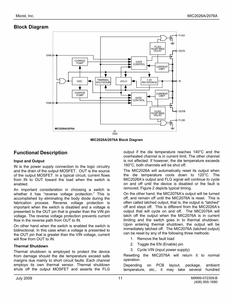
Block Diagram
MIC2026A/2076A Block Diagram
Functional Description
Input and Output IN is the power supply connection to the logic circuitry and the drain of the output MOSFET. OUT is the source of the output MOSFET. In a typical circuit, current flows from IN to OUT toward the load when the switch is enabled.
An important consideration in choosing a switch is whether it has “reverse voltage protection.” This is accomplished by eliminating the body diode during the fabrication process. Reverse voltage protection is important when the switch is disabled and a voltage is presented to the OUT pin that is greater than the VIN pin voltage. The reverse voltage protection prevents current flow in the reverse path from OUT to IN. On other hand when the switch is enabled the switch is bidirectional. In this case when a voltage is presented to the OUT pin that is greater than the VIN voltage, current will flow from OUT to IN.
Thermal Shutdown Thermal shutdown is employed to protect the device from damage should the die temperature exceed safe margins due mainly to short circuit faults. Each channel employs its own thermal sensor. Thermal shutdown shuts off the output MOSFET and asserts the FLG
output if the die temperature reaches 140°C and the overheated channel is in current limit. The other channel is not affected. If however, the die temperature exceeds 160°C, both channels will be shut off. The MIC2026A will automatically reset its output when the die temperature cools down to 120°C. The MIC2026A’s output and FLG signal will continue to cycle on and off until the device is disabled or the fault is removed. Figure 2 depicts typical timing. On the other hand, the MIC2076A’s output will be turned off, and remain off until the MIC2076A is reset. This is often called latched output, that is, the output is “latched” off and stays off. This is different from the MIC2026A’s output that will cycle on and off. The MIC2076A will latch off the output when the MIC2076A is in current limiting and the switch goes in to thermal shutdown. Upon entering thermal shutdown, the output will be immediately latched off. The MIC2076A (latched output) can be reset by any of the following three methods:
1. Remove the fault load 2. Toggle the EN (Enable) pin 3. Cycle VIN (input power supply)
Resetting the MIC2076A will return it to normal operation. Depending on PCB layout, package, ambient temperature, etc., it may take several hundred

Micrel, Inc. MIC2026A/2076A
July 2009 12 M9999-072309-B(408) 955-1690
milliseconds from the incidence of the fault to the output MOSFET being shut off. This time will be shortest in the case of a dead short on the output. Power Dissipation The device’s junction temperature depends on several factors such as the load, PCB layout, ambient temperature, and package type. Equations that can be used to calculate power dissipation of each channel and junction temperature are found below:
PD = RDS(on) x IOUT2
Total power dissipation of the device will be the summation of PD for both channels. To relate this to junction temperature, the following equation can be used:
TJ = PD × θJA + TA
where: TJ = junction temperature TA = ambient temperature θJA = is the thermal resistance of the package
Current Sensing and Limiting The current-limit threshold is preset internally. The preset level prevents damage to the device and external load but still allows a minimum current of 500mA to be delivered to the load. The current-limit circuit senses a portion of the output MOSFET switch current. The current-sense resistor shown in the block diagram is a virtual and has no voltage drop. The reaction to an overcurrent condition varies with three scenarios:
• Switch Enabled into Short-Circuit If a switch is enabled into a heavy load or short-circuit, the switch immediately enters into a constant-current mode, reducing the output voltage. The FLG signal is asserted indicating an overcurrent condition.
• Short-Circuit Applied to Enabled Output When a heavy load or short-circuit is applied to an enabled switch, a large transient current may flow until the current-limit circuitry responds. Once this occurs, the device limits current to the short-circuit current limit specification.
• Current-Limit Response The MIC2026A/2076A current-limit response is often called the foldback current-limit. The foldback current-limit is the current limit reached when the output current is increased slowly rather than abruptly. An approximation of slowly is tens of milliamps per second. The foldback current-limit is typical 200 mA higher than the short-circuit current-limit. When the foldback current-limit is reached, the output current will abruptly decrease to the short-circuit current-limit.
Fault Flag The FLG signal is an N-Channel open-drain MOSFET output. FLG is asserted (active-low) when either an overcurrent or thermal shutdown condition occurs. In the case of an overcurrent condition, FLG will be asserted only after the flag response delay time, tD, has elapsed. This ensures that FLG is asserted only upon valid overcurrent conditions and that erroneous error reporting is eliminated. For example, false overcurrent conditions can occur during hot plug events when a highly capacitive load is connected and causes a high transient inrush current that exceeds the current-limit threshold for up to 1ms. The FLG response delay time tD is typically 3ms.
Undervoltage Lockout Undervoltage lockout (UVLO) prevents the output MOSFET from turning on until VIN exceeds approximately 2.45V. Undervoltage detection functions only when the switch is enabled.
Figure 1. MIC2076A Fault Timing: Output Reset by Removing Load

Micrel, Inc. MIC2026A/2076A
July 2009 13 M9999-072309-B(408) 955-1690
Figure 2. MIC2026A Fault Timing
Application Information Supply Filtering A 0.1µF to 1µF bypass capacitor positioned close to VIN and GND pins of the device is strongly recommended to control supply transients. Without a bypass capacitor, an output short may cause sufficient ringing on the input (from supply lead inductance) to damage internal control circuitry.
Printed Circuit Board Hot-Plug The MIC2026A/2076A are ideal inrush current-limiters for hot plug applications. Due to their integrated charge pumps, the MIC2026A/2076A present a high impedance when off and slowly become a low impedance as their integrated charge pumps turn on. This “soft-start” feature effectively isolates power supplies from highly capacitive loads by reducing inrush current. Figure 3 shows how the MIC2026A may be used in a card hot-plug application. In cases of extremely large capacitive loads (>400µF), the length of the transient due to inrush current may exceed the delay provided by the integrated filter. Since this inrush current exceeds the current-limit delay specification, FLG will be asserted during this time. To prevent the logic controller from responding to FLG being asserted, an external RC filter, as shown in Figure 4, can be used to filter out transient FLG assertion. The value of the RC time constant should be selected to match the length of the transient, less tD(min) of the MIC2026A/2076A.
Universal Serial Bus (USB) Power Distribution The MIC2026A/2076A are ideally suited for USB (Universal Serial Bus) power distribution applications. The USB specification defines power distribution for USB host systems such as PCs and USB hubs. Hubs can either be self-powered or bus-powered (that is, powered from the bus). Figure 5 shows a typical USB Host application that may be suited for mobile PC applications employing USB. The requirement for USB host systems is that the port must supply a minimum of 500mA at an output voltage of 5V ±5%. In addition, the output power delivered must be limited to below 25VA. Upon an overcurrent condition, the host must also be notified. To support hot-plug events, the hub must have a minimum of 120µF of bulk capacitance, preferably low ESR electrolytic or tantalum. Please refer to Application Note 17 for more details on designing compliant USB hub and host systems. For bus-powered hubs, USB requires that each downstream port be switched on or off under control by the host. Up to four downstream ports each capable of supplying 100mA at 4.4V minimum are allowed. In addition, to reduce voltage droop on the upstream VBUS, soft-start is necessary. Although the hub can consume up to 500mA from the upstream bus, the hub must consume only 100mA max at start-up, until it enumerates with the host prior to requesting more power. The same requirements apply for bus-powered peripherals that have no downstream ports. Figure 6 shows a bus-powered hub.

Micrel, Inc. MIC2026A/2076A
July 2009 14 M9999-072309-B(408) 955-1690
Figure 3. Hot-Plug Application
Figure 4. Transient Filter

Micrel, Inc. MIC2026A/2076A
July 2009 15 M9999-072309-B(408) 955-1690
Figure 5. USB Two-Port Host Application
Figure 6. USB Two-Port Bus-Powered Hub
Micrel, Inc. MIC2026A/2076A
July 2009 16 M9999-072309-B(408) 955-1690
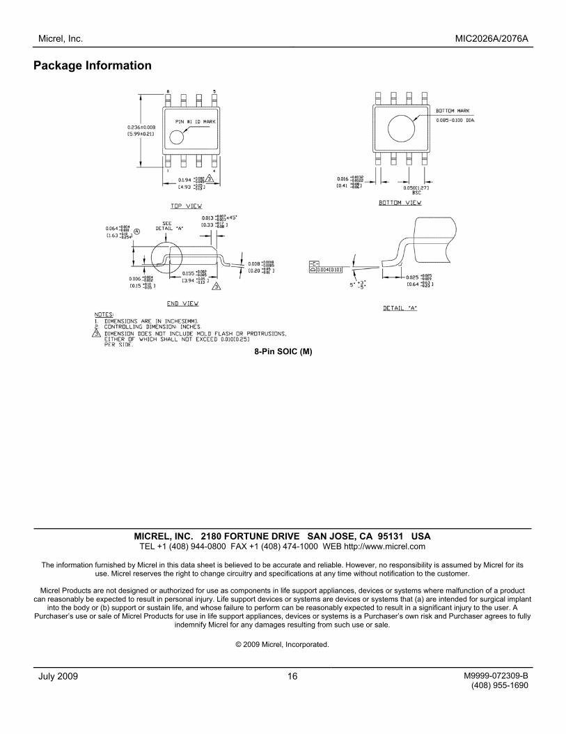
Package Information
8-Pin SOIC (M)
MICREL, INC. 2180 FORTUNE DRIVE SAN JOSE, CA 95131 USA TEL +1 (408) 944-0800 FAX +1 (408) 474-1000 WEB http://www.micrel.com
The information furnished by Micrel in this data sheet is believed to be accurate and reliable. However, no responsibility is assumed by Micrel for its
use. Micrel reserves the right to change circuitry and specifications at any time without notification to the customer.
Micrel Products are not designed or authorized for use as components in life support appliances, devices or systems where malfunction of a product reasonably be expected to result in personal injury. Life support devices or systems are devices or systems that (a) are intended for surgical implainto the body or (b) support or sustain life, and whose failure to perform can be reasonably expected to result in a significant injury to the user. A
Purchaser’s use or sale of Micrel Products for use in life support appliances, devices or systems is a Purchaser’s own risk and Purchaser agrees to fully indemnify Micrel for any damages resulting from such use or sale.
can nt
© 2009 Micrel, Incorporated.