[email protected]://csce.uark.edu +1 (479) 575-6043
CAD Design FlowCourtesy of Dr. Sung Kyu Lim@Gatech, Dr. Daehyun Lim@WSU, Dr. Shmuel Wimer @ Bar Ilan Univ. and Dr. Igor Markov@UMich
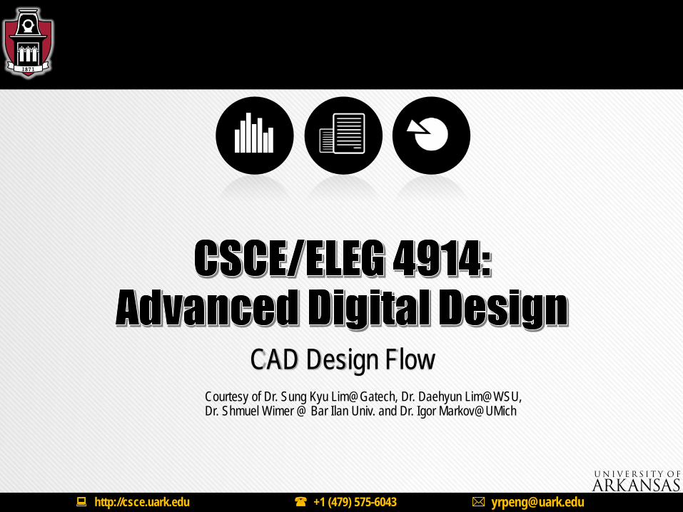
Electronic Design Automation (EDA)
15.7 20.3 19.4 26.3 32.9 44.929.5 39.8
25.2 32.6 27.0 36.916.9 23.1 31.7
43.529.6
40.756.4
79.033.6
46.7
31.142.5
27.235.2 34.0
46.6
21.429.4
40.5
55.7
0.0
20.0
40.0
60.0
80.0
100.0
120.0
2009 2010 2011 2012 2013 2014 2015 2016 2017 2018 2019 2020 2021 2022 2023 2024
ITRS 2009 Cost Chart(in Millions of Dollars)
Total HW Engineering Costs + EDA Tool Costs Total SW Engineering Costs + ESDA Tool Costs
ITRS 2009 Cost Chart(in Millions of Dollars)
Total HW Engineering Costs + EDA Tool Costs Total SW Engineering Costs + ESDA Tool Costs
Impact of EDA technologies on overall IC design productivity and IC design cost
9/5/2017 CSCE/ELEG 4914: Advnaced Digital Design 2

History of EDA
Design for Manufacturability (DFM), optical proximity correction (OPC), and other techniques emerge at the design-manufacturing interface. Increased reusability of blocks, including intellectual property (IP) blocks.
2000 - now
First over-the-cell routing, first 3D and multilayer placement and routing techniques developed. Automated circuit synthesis and routability-oriented design become dominant. Start of parallelizing workloads. Emergence of physical synthesis.
1990 -2000
First performance-driven tools and parallel optimization algorithms for layout; better understanding of underlying theory (graph theory, solution complexity, etc.).
1985 -1990
More advanced tools for ICs and PCBs, with more sophisticated algorithms.1975 -1985
Layout editors, e.g., place and route tools, first developed for printed circuit boards.1965 -1975
Manual design only. 1950 -1965
Circuit and Physical Design Process AdvancementsTime Period
© 2
011
Sprin
ger V
erla
g
9/5/2017 CSCE/ELEG 4914: Advnaced Digital Design 3

VLSI Semi-Custom Design Flow
C/C++, System Verilog
Gate-level Netlist
Bare die
Chip
System Specification
Architecture Design
Circuit Design
Synthesis
Physical Design
Fabrication
Testing & Packaging
Verification Tape-out
RTL Netlist
System Model
Verilog, VHDL
Verilog, VHDL, Spice
LEF/DEF, Milkyway, OpenAcess
GDSII, OASIS
Layout
AIF,ODB++
64-bit Processor
9/5/2017 CSCE/ELEG 4914: Advnaced Digital Design 4

Structured Design
How to design VLSI chips?●Many millions (even billions!) of transistors●Tens to hundreds of engineersHierarchy: Divide and Conquer●Recursively system into modulesRegularity●Reuse modules wherever possible●Ex: Standard cell libraryModularity: well-formed interfaces●Allows modules to be treated as black boxes Locality●Physical and temporal
9/5/2017 CSCE/ELEG 4914: Advnaced Digital Design 5

Design Partitioning
Architecture: User’s perspective, what does it do?● Instruction set, registers●MIPS, x86, Alpha, PIC, ARM, …Microarchitecture●Single cycle, multcycle, pipelined, superscalar? Logic: how are functional blocks constructed●Ripple carry, carry lookahead, carry select addersCircuit: how are transistors used●Complementary CMOS, pass transistors, domino Physical: chip layout●Datapaths, memories, random logic
9/5/2017 CSCE/ELEG 4914: Advnaced Digital Design 6

MIPS Microarchitecture
Multicycle µarchitecture ( [Paterson04], [Harris07] )
9/5/2017 CSCE/ELEG 4914: Advnaced Digital Design 7
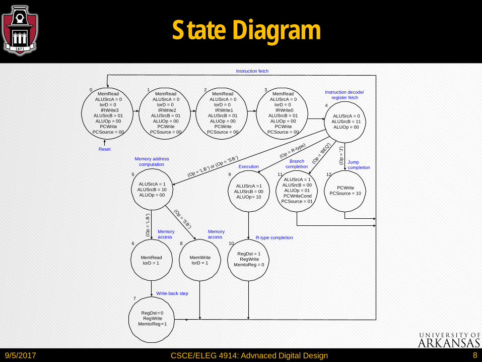
State Diagram
PCWritePCSource = 10
ALUSrcA = 1ALUSrcB = 00ALUOp = 01PCWriteCond
PCSource = 01
ALUSrcA =1ALUSrcB = 00ALUOp= 10
RegDst = 1RegWrite
MemtoReg = 0MemWriteIorD = 1
MemReadIorD = 1
ALUSrcA = 1ALUSrcB = 10ALUOp = 00
RegDst= 0RegWrite
MemtoReg =1
ALUSrcA = 0ALUSrcB = 11ALUOp = 00
MemReadALUSrcA = 0
IorD = 0IRWrite3
ALUSrcB = 01ALUOp = 00
PCWritePCSource = 00
Instruction fetch
Instruction decode/register fetch
Jumpcompletion
BranchcompletionExecution
Memory addresscomputation
Memoryaccess
Memoryaccess R-type completion
Write-back step
(Op = 'LB ') or (Op = 'SB ') (Op = R-type)
(Op = 'BEQ')
(Op
='J
')
(Op = 'S B')
(Op
='L
B')
7
0
4
121195
1086
Reset
MemReadALUSrcA = 0
IorD = 0IRWrite2
ALUSrcB = 01ALUOp = 00
PCWritePCSource = 00
1MemRead
ALUSrcA = 0IorD = 0IRWrite1
ALUSrcB = 01ALUOp = 00
PCWritePCSource = 00
2MemRead
ALUSrcA = 0IorD = 0IRWrite0
ALUSrcB = 01ALUOp = 00
PCWritePCSource = 00
3
9/5/2017 CSCE/ELEG 4914: Advnaced Digital Design 8

Block Diagram
9/5/2017 CSCE/ELEG 4914: Advnaced Digital Design 9

Hierarchical Design
mips
controller alucontrol datapath
standardcell library
bitslice zipper
alu
and2
flopinv4x
mux2
mux4
ramslice
fulladder
nand2nor2
or2
inv
tri
9/5/2017 CSCE/ELEG 4914: Advnaced Digital Design 10

HDLs
Hardware Description Languages●Widely used in logic design●Verilog and VHDLDescribe hardware using code●Document logic functions●Simulate logic before building●Synthesize code into gates and layout
▪ Requires a library of standard cells
9/5/2017 CSCE/ELEG 4914: Advnaced Digital Design 11
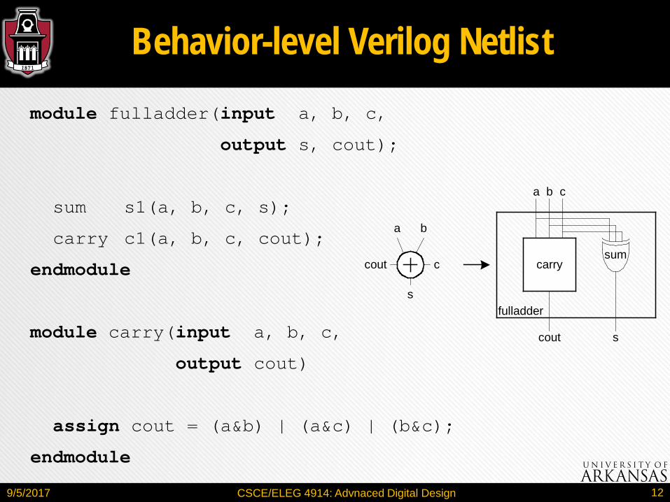
Behavior-level Verilog Netlistmodule fulladder(input a, b, c,
output s, cout);
sum s1(a, b, c, s);
carry c1(a, b, c, cout);
endmodule
module carry(input a, b, c,
output cout)
assign cout = (a&b) | (a&c) | (b&c);
endmodule
a b
c
s
cout carrysum
s
a b c
cout
fulladder
9/5/2017 CSCE/ELEG 4914: Advnaced Digital Design 12

Gate-level Verilog Netlist
module carry(input a, b, c, output cout)
wire x, y, z;
and g1(x, a, b);and g2(y, a, c);and g3(z, b, c);or g4(cout, x, y, z);
endmodule
ab
ac
bc
cout
x
y
z
g1
g2
g3
g4
9/5/2017 CSCE/ELEG 4914: Advnaced Digital Design 13
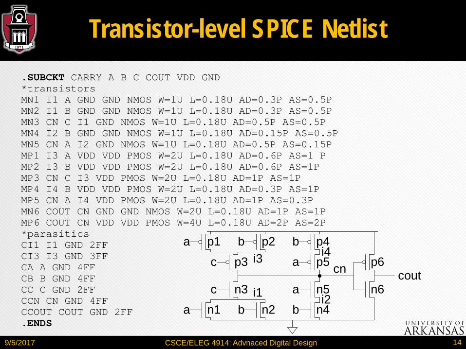
Transistor-level SPICE Netlist.SUBCKT CARRY A B C COUT VDD GND*transistorsMN1 I1 A GND GND NMOS W=1U L=0.18U AD=0.3P AS=0.5PMN2 I1 B GND GND NMOS W=1U L=0.18U AD=0.3P AS=0.5PMN3 CN C I1 GND NMOS W=1U L=0.18U AD=0.5P AS=0.5PMN4 I2 B GND GND NMOS W=1U L=0.18U AD=0.15P AS=0.5PMN5 CN A I2 GND NMOS W=1U L=0.18U AD=0.5P AS=0.15PMP1 I3 A VDD VDD PMOS W=2U L=0.18U AD=0.6P AS=1 PMP2 I3 B VDD VDD PMOS W=2U L=0.18U AD=0.6P AS=1PMP3 CN C I3 VDD PMOS W=2U L=0.18U AD=1P AS=1PMP4 I4 B VDD VDD PMOS W=2U L=0.18U AD=0.3P AS=1PMP5 CN A I4 VDD PMOS W=2U L=0.18U AD=1P AS=0.3PMN6 COUT CN GND GND NMOS W=2U L=0.18U AD=1P AS=1PMP6 COUT CN VDD VDD PMOS W=4U L=0.18U AD=2P AS=2P*parasiticsCI1 I1 GND 2FFCI3 I3 GND 3FFCA A GND 4FFCB B GND 4FFCC C GND 2FFCCN CN GND 4FFCCOUT COUT GND 2FF.ENDS
a bc
ca b
ba
ab
coutcn
n1 n2n3
n4n5 n6
p6p5p4
p3p2p1
i1
i3
i2
i4
9/5/2017 CSCE/ELEG 4914: Advnaced Digital Design 14

Physical Design FlowSystem Specification
Architecture Design
Circuit Design
Synthesis
Physical Design
Fabrication
Testing & Packaging
Verification
Floorplanning
Placement
Signal Routing
Partitioning
Timing Closure
Clock Tree Synthesis
9/5/2017 CSCE/ELEG 4914: Advnaced Digital Design 15

Standard Cells
Uniform cell heightUniform well heightM1 VDD and GND railsM2 Access to I/OsWell / substrate taps Exploits regularity
9/5/2017 CSCE/ELEG 4914: Advnaced Digital Design 16
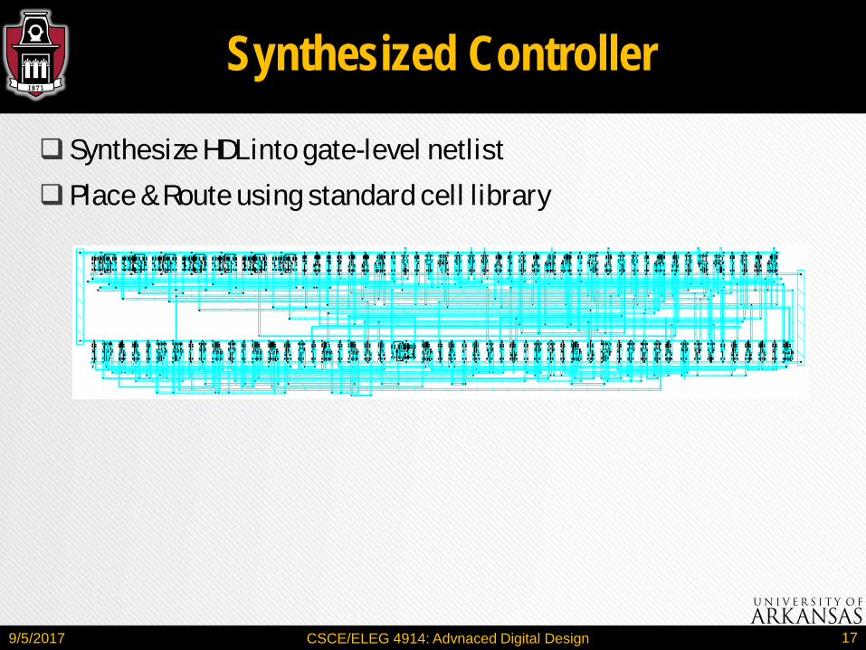
Synthesized Controller
Synthesize HDL into gate-level netlist Place & Route using standard cell library
9/5/2017 CSCE/ELEG 4914: Advnaced Digital Design 17

MIPS Floorplan
9/5/2017 CSCE/ELEG 4914: Advnaced Digital Design 18

MIPS Layout
9/5/2017 CSCE/ELEG 4914: Advnaced Digital Design 19
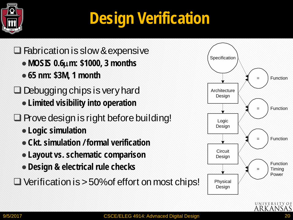
Design Verification
Fabrication is slow & expensive●MOSIS 0.6µm: $1000, 3 months●65 nm: $3M, 1 monthDebugging chips is very hard●Limited visibility into operation Prove design is right before building!●Logic simulation●Ckt. simulation / formal verification●Layout vs. schematic comparison●Design & electrical rule checks Verification is > 50% of effort on most chips!
Specification
ArchitectureDesign
LogicDesign
CircuitDesign
PhysicalDesign
=
=
=
=
Function
Function
Function
FunctionTimingPower
9/5/2017 CSCE/ELEG 4914: Advnaced Digital Design 20

Fabrication & Packaging Tapeout final layout Fabrication
● 6, 8, 12” wafers● Optimized for throughput,
not latency (10 weeks!)● Cut into individual dice
Packaging● Bond gold wires from die I/O pads to package
9/5/2017 CSCE/ELEG 4914: Advnaced Digital Design 21

Testing
Test that chip operates●Design errors●Manufacturing errors A single dust particle or wafer defect kills a die●Yields from 90% to < 10%●Depends on die size, maturity of process●Test each part before shipping to customer
9/5/2017 CSCE/ELEG 4914: Advnaced Digital Design 22

Matrix Solver (20K Cells)●Cadence Encounter: placement (1 sec), routing (12 sec)●Area = 72x72um (45nm library), used 6 metal layers
Design Example
9/5/2017 CSCE/ELEG 4914: Advnaced Digital Design 23

Matrix Solver
Design Example
9/5/2017 CSCE/ELEG 4914: Advnaced Digital Design 24

Large designs need to be partitioned into hierarchical blocks●Allows each block to be designed separately●Limit the complexity of each sub-design and optimize interconnects
Hierarchical Design
9/5/2017 CSCE/ELEG 4914: Advnaced Digital Design 25
Recommended