AN11524NXQ1TXA6 Evaluation BoardRev. 1 — 17 February 2015 Application note
Document information
Info Content
Keywords NXQ1TXA6, NWP2081, Wireless Charging, Qi, mobile devices, base station, magnetic coupled power transfer
Abstract This document illustrates how to create a Qi A6 wireless power base station. It uses the NXQ1TXA6 charging controller and its evaluation board that can deliver up to 5 W effective output at the wireless mobile device side
NXP Semiconductors AN11524NXQ1TXA6 Evaluation Board
Revision history
Rev Date Description
v. 1.0 20150217 Initial version
AN11524 All information provided in this document is subject to legal disclaimers. © NXP Semiconductors N.V. 2015. All rights reserved.
Application note Rev. 1 — 17 February 2015 2 of 54
Contact informationFor more information, please visit: http://www.nxp.com
For sales office addresses, please send an email to: [email protected]
NXP Semiconductors AN11524NXQ1TXA6 Evaluation Board
1. Introduction
The ubiquity of mobile phones, increases the requirement of a convenient way to charge these devices while on the move. Especially the fast rising number of smart phones widely used and relied upon in daily life. Wireless charging is introduced into smart phones and tablets.
Wireless charging represents the future of public and private charging.
Qi (pronounced as "Chee") is a wireless charging standard developed by Wireless Power Consortium (www.wirelesspowerconsortium.com) for inductive power.
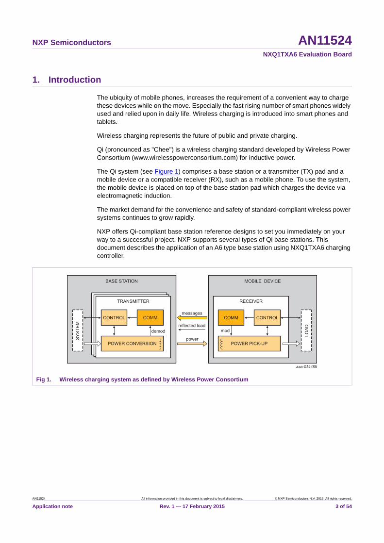
The Qi system (see Figure 1) comprises a base station or a transmitter (TX) pad and a mobile device or a compatible receiver (RX), such as a mobile phone. To use the system, the mobile device is placed on top of the base station pad which charges the device via electromagnetic induction.
The market demand for the convenience and safety of standard-compliant wireless power systems continues to grow rapidly.
NXP offers Qi-compliant base station reference designs to set you immediately on your way to a successful project. NXP supports several types of Qi base stations. This document describes the application of an A6 type base station using NXQ1TXA6 charging controller.
Fig 1. Wireless charging system as defined by Wireless Power Consortium
aaa-014485
BASE STATION
TRANSMITTER
COMMmessages
reflected load
power
CONTROL
SY
STE
M
POWER CONVERSION
demod
MOBILE DEVICE
RECEIVER
CONTROLCOMM
LOA
D
POWER PICK-UP
mod
AN11524 All information provided in this document is subject to legal disclaimers. © NXP Semiconductors N.V. 2015. All rights reserved.
Application note Rev. 1 — 17 February 2015 3 of 54
NXP Semiconductors AN11524NXQ1TXA6 Evaluation Board
2. Scope
This document discusses the design of a WPC Qi A6 type base station based on the NXP NXQ1TXA6 Evaluation Board. The NXQ1TXA6 Evaluation Board is Qi certified and it complies with EMI regulation - EN55022 and FCC part 18.
The document is intended to provide engineers with real life practical design applications and get them started on the right note immediately.
For all topics covered, hints are provided to ensure system-level best performance, excellent EMC and lowest application cost.
Near Field Communication (NFC) option for tap to power on to enable zero power standby and Bluetooth pairing is included. There are many other use cases and possibilities with NFC technology but they are not within the scope of this application note.
AN11524 All information provided in this document is subject to legal disclaimers. © NXP Semiconductors N.V. 2015. All rights reserved.
Application note Rev. 1 — 17 February 2015 4 of 54
NXP Semiconductors AN11524NXQ1TXA6 Evaluation Board
3. Getting started
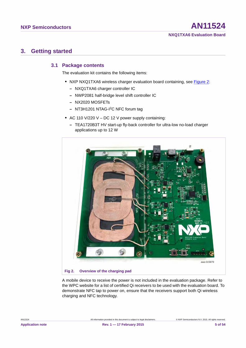
3.1 Package contents
The evaluation kit contains the following items:
• NXP NXQ1TXA6 wireless charger evaluation board containing, see Figure 2:
– NXQ1TXA6 charger controller IC
– NWP2081 half-bridge level shift controller IC
– NX2020 MOSFETs
– NT3H1201 NTAG-I2C NFC forum tag
• AC 110 V/220 V – DC 12 V power supply containing:
– TEA1720B3T HV start-up fly-back controller for ultra-low no-load charger applications up to 12 W
A mobile device to receive the power is not included in the evaluation package. Refer to the WPC website for a list of certified Qi receivers to be used with the evaluation board. To demonstrate NFC tap to power on, ensure that the receivers support both Qi wireless charging and NFC technology.
Fig 2. Overview of the charging pad
aaa-015876
AN11524 All information provided in this document is subject to legal disclaimers. © NXP Semiconductors N.V. 2015. All rights reserved.
Application note Rev. 1 — 17 February 2015 5 of 54
NXP Semiconductors AN11524NXQ1TXA6 Evaluation Board
3.2 Main features
The NXQ1TXA6 Evaluation Board demonstrates:
• A reference design with key components from NXP for wireless charging applications based on inductive power transfer standard Qi.
• Shows additional benefits resulting from integration of NFC with wireless charging. Enabling for example zero power standby with the “tap to power on” feature.
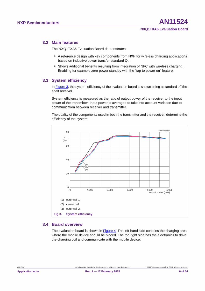
3.3 System efficiency
In Figure 3, the system efficiency of the evaluation board is shown using a standard off the shelf receiver.
System efficiency is measured as the ratio of output power of the receiver to the input power of the transmitter. Input power is averaged to take into account variation due to communication between receiver and transmitter.
The quality of the components used in both the transmitter and the receiver, determine the efficiency of the system.
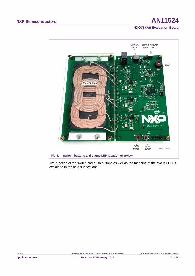
3.4 Board overview
The evaluation board is shown in Figure 4. The left-hand side contains the charging area where the mobile device should be placed. The top right side has the electronics to drive the charging coil and communicate with the mobile device.
(1) outer coil 1
(2) center coil
(3) outer coil 2
Fig 3. System efficiency
output power (mW)0 5,0004,0002,000 3,0001,000
aaa-015880
40
20
60
80
η(%)
0
(1)(2)(3)
AN11524 All information provided in this document is subject to legal disclaimers. © NXP Semiconductors N.V. 2015. All rights reserved.
Application note Rev. 1 — 17 February 2015 6 of 54
NXP Semiconductors AN11524NXQ1TXA6 Evaluation Board
The function of the switch and push buttons as well as the meaning of the status LED is explained in the next subsections.
Fig 4. Switch, buttons and status LED location overview
aaa-015882
LED
stand-by powermode switch
12 V DCinput
FODbutton
resetbutton
charging area
AN11524 All information provided in this document is subject to legal disclaimers. © NXP Semiconductors N.V. 2015. All rights reserved.
Application note Rev. 1 — 17 February 2015 7 of 54
NXP Semiconductors AN11524NXQ1TXA6 Evaluation Board
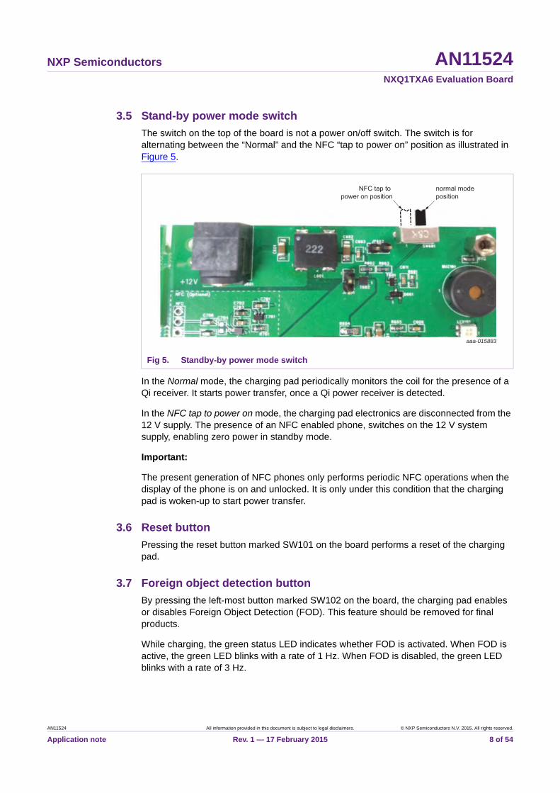
3.5 Stand-by power mode switch
The switch on the top of the board is not a power on/off switch. The switch is for alternating between the “Normal” and the NFC “tap to power on” position as illustrated in Figure 5.
In the Normal mode, the charging pad periodically monitors the coil for the presence of a Qi receiver. It starts power transfer, once a Qi power receiver is detected.
In the NFC tap to power on mode, the charging pad electronics are disconnected from the 12 V supply. The presence of an NFC enabled phone, switches on the 12 V system supply, enabling zero power in standby mode.
Important:
The present generation of NFC phones only performs periodic NFC operations when the display of the phone is on and unlocked. It is only under this condition that the charging pad is woken-up to start power transfer.
3.6 Reset button
Pressing the reset button marked SW101 on the board performs a reset of the charging pad.
3.7 Foreign object detection button
By pressing the left-most button marked SW102 on the board, the charging pad enables or disables Foreign Object Detection (FOD). This feature should be removed for final products.
While charging, the green status LED indicates whether FOD is activated. When FOD is active, the green LED blinks with a rate of 1 Hz. When FOD is disabled, the green LED blinks with a rate of 3 Hz.
Fig 5. Standby-by power mode switch
aaa-015883
normal modeposition
NFC tap to power on position
AN11524 All information provided in this document is subject to legal disclaimers. © NXP Semiconductors N.V. 2015. All rights reserved.
Application note Rev. 1 — 17 February 2015 8 of 54
NXP Semiconductors AN11524NXQ1TXA6 Evaluation Board
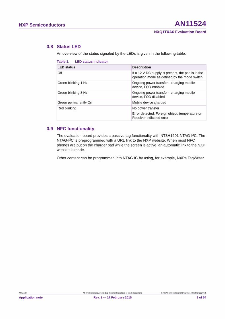
3.8 Status LED
An overview of the status signaled by the LEDs is given in the following table:
3.9 NFC functionality
The evaluation board provides a passive tag functionality with NT3H1201 NTAG-I2C. The NTAG-I2C is preprogrammed with a URL link to the NXP website. When most NFC phones are put on the charger pad while the screen is active, an automatic link to the NXP website is made.
Other content can be programmed into NTAG IC by using, for example, NXPs TagWriter.
Table 1. LED status indicator
LED status Description
Off If a 12 V DC supply is present, the pad is in the operation mode as defined by the mode switch
Green blinking 1 Hz Ongoing power transfer - charging mobile device, FOD enabled
Green blinking 3 Hz Ongoing power transfer - charging mobile device, FOD disabled
Green permanently On Mobile device charged
Red blinking No power transfer
Error detected: Foreign object, temperature or Receiver indicated error
AN11524 All information provided in this document is subject to legal disclaimers. © NXP Semiconductors N.V. 2015. All rights reserved.
Application note Rev. 1 — 17 February 2015 9 of 54
NXP Semiconductors AN11524NXQ1TXA6 Evaluation Board
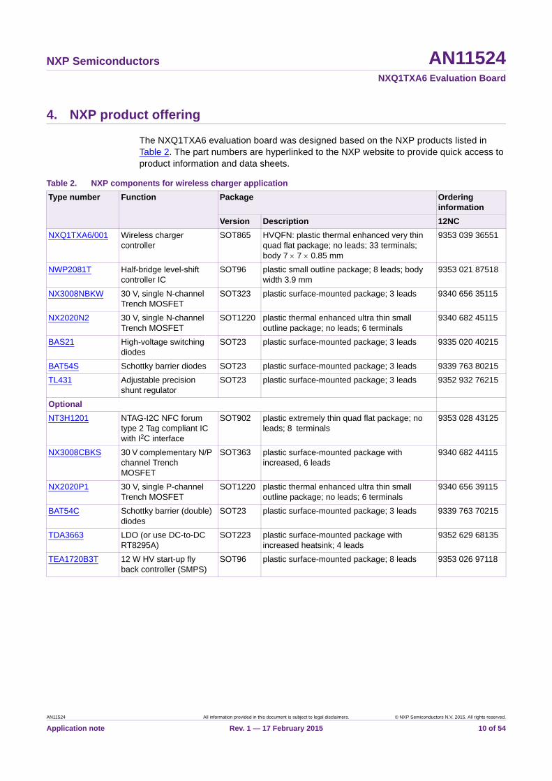
4. NXP product offering
The NXQ1TXA6 evaluation board was designed based on the NXP products listed in Table 2. The part numbers are hyperlinked to the NXP website to provide quick access to product information and data sheets.
Table 2. NXP components for wireless charger application
Type number Function Package Ordering information
Version Description 12NC
NXQ1TXA6/001 Wireless charger controller
SOT865 HVQFN: plastic thermal enhanced very thin quad flat package; no leads; 33 terminals; body 7 7 0.85 mm
9353 039 36551
NWP2081T Half-bridge level-shift controller IC
SOT96 plastic small outline package; 8 leads; body width 3.9 mm
9353 021 87518
NX3008NBKW 30 V, single N-channel Trench MOSFET
SOT323 plastic surface-mounted package; 3 leads 9340 656 35115
NX2020N2 30 V, single N-channel Trench MOSFET
SOT1220 plastic thermal enhanced ultra thin small outline package; no leads; 6 terminals
9340 682 45115
BAS21 High-voltage switching diodes
SOT23 plastic surface-mounted package; 3 leads 9335 020 40215
BAT54S Schottky barrier diodes SOT23 plastic surface-mounted package; 3 leads 9339 763 80215
TL431 Adjustable precision shunt regulator
SOT23 plastic surface-mounted package; 3 leads 9352 932 76215
Optional
NT3H1201 NTAG-I2C NFC forum type 2 Tag compliant IC with I2C interface
SOT902 plastic extremely thin quad flat package; no leads; 8 terminals
9353 028 43125
NX3008CBKS 30 V complementary N/P channel Trench MOSFET
SOT363 plastic surface-mounted package with increased, 6 leads
9340 682 44115
NX2020P1 30 V, single P-channel Trench MOSFET
SOT1220 plastic thermal enhanced ultra thin small outline package; no leads; 6 terminals
9340 656 39115
BAT54C Schottky barrier (double) diodes
SOT23 plastic surface-mounted package; 3 leads 9339 763 70215
TDA3663 LDO (or use DC-to-DC RT8295A)
SOT223 plastic surface-mounted package with increased heatsink; 4 leads
9352 629 68135
TEA1720B3T 12 W HV start-up fly back controller (SMPS)
SOT96 plastic surface-mounted package; 8 leads 9353 026 97118
AN11524 All information provided in this document is subject to legal disclaimers. © NXP Semiconductors N.V. 2015. All rights reserved.
Application note Rev. 1 — 17 February 2015 10 of 54
NXP Semiconductors AN11524NXQ1TXA6 Evaluation Board
5. System overview
The NXQ1TXA6 Evaluation Board is a WPC Qi A6 type base station, powered by a +12 V AC-to-DC adapter.
It works on the basic principle of inductively coupled power transfer. An alternating current generated from the half-bridge driver is passed through the base station coil. It creates a magnetic field which induces a voltage in the mobile device coil. The mobile device communicates information related to power management and control to the base station.
When the NFC tap to power on feature is enabled, the evaluation board consumes zero power in standby mode.
A block diagram of the NXQ1TXA6 evaluation board is depicted in Figure 6. Each subblock is described in Section 5.1 to Section 5.8.
AN11524 All information provided in this document is subject to legal disclaimers. © NXP Semiconductors N.V. 2015. All rights reserved.
Application note Rev. 1 — 17 February 2015 11 of 54
NXP Semiconductors AN11524NXQ1TXA6 Evaluation Board
The block diagram does not depict all semiconductor components used to build up the system. See the related application note for details.
The NXQ1TXA6/001 supports the A6 single-coil and 3-coil configurations.
Fig 6. NXQ1TXA6 evaluation board block diagram
aaa-014209
NFC TAG IF
NXQ1TXA6
UI CTRL
NXP component
Optional NXP components forNFC control and zero standby power
MONITOR
HALF-BRIDGECONTROL
CONTROLLER
DEMODULATOR ASK DETECTION
MODE SELECT
MODE SELECTAND
VOLTAGEREFERENCE
SE
L3
SE
L2
SE
L1
OP
T2
OP
T1
CL_MON
ASK
HALF-BRIDGEDRIVER
EN_HB1
EN_HB2
EN_HB3
PWM
3V3
Vout
VS
NS
ISN
S
NTC
NWP2081
EN
_NFC
3V3
3V3
RESET
LED1
LED2
DC/DC
NX3008NBKW
NX2020P1
NX2020N2
3 x BAS21
NX2020N2
HALF-BRIDGEDRIVER
NWP2081
NX2020N2
NX2020N2
HALF-BRIDGEDRIVER
NWP2081
NX2020N2
NX2020N2
RSense12 V
OPTIONAL
CURRENTMONITOR
NFCNT3H1201
AC/DCTEA1720
mains110 - 230 V ~
(TL431BFDT)
BU
ZZ
buzzer
l2C
NX3008CBKS
AN11524 All information provided in this document is subject to legal disclaimers. © NXP Semiconductors N.V. 2015. All rights reserved.
Application note Rev. 1 — 17 February 2015 12 of 54
NXP Semiconductors AN11524NXQ1TXA6 Evaluation Board
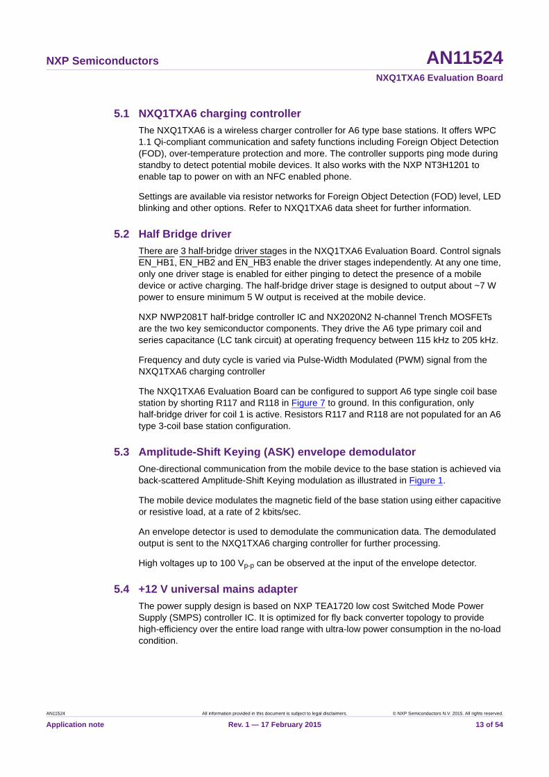
5.1 NXQ1TXA6 charging controller
The NXQ1TXA6 is a wireless charger controller for A6 type base stations. It offers WPC 1.1 Qi-compliant communication and safety functions including Foreign Object Detection (FOD), over-temperature protection and more. The controller supports ping mode during standby to detect potential mobile devices. It also works with the NXP NT3H1201 to enable tap to power on with an NFC enabled phone.
Settings are available via resistor networks for Foreign Object Detection (FOD) level, LED blinking and other options. Refer to NXQ1TXA6 data sheet for further information.
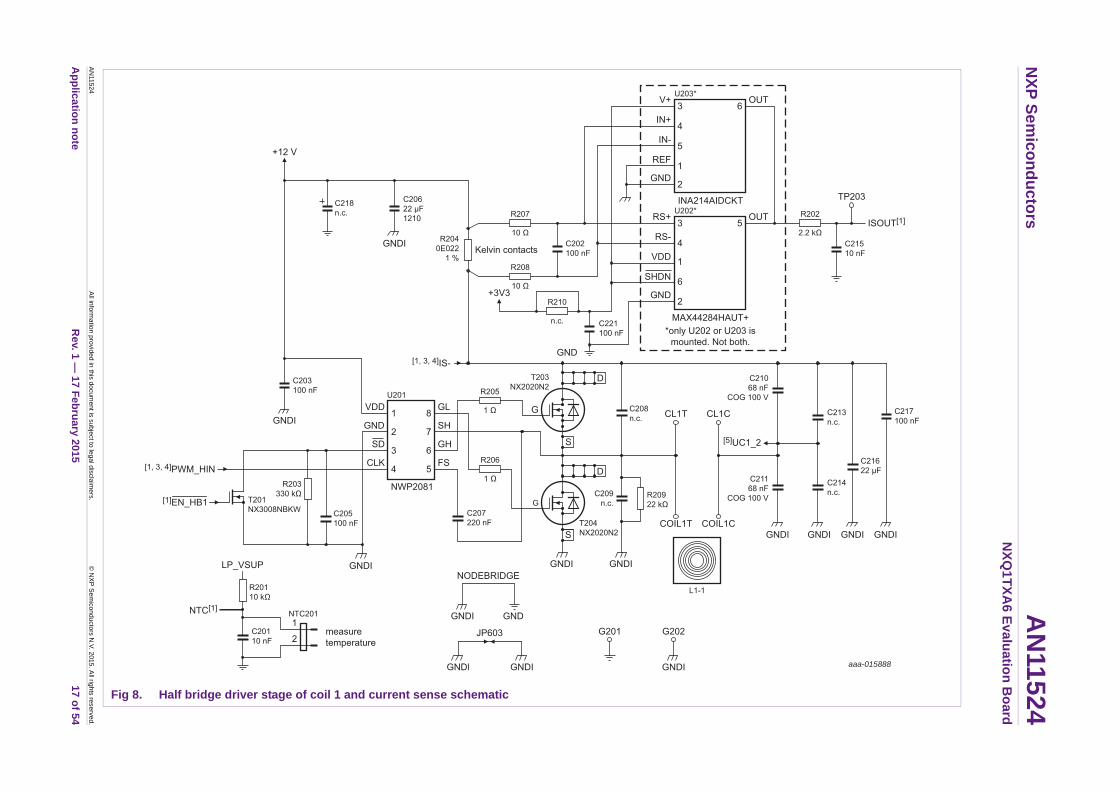
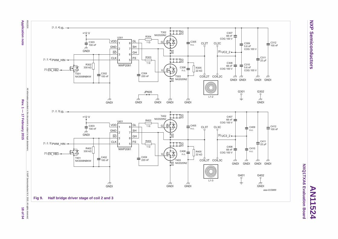
5.2 Half Bridge driver
There are 3 half-bridge driver stages in the NXQ1TXA6 Evaluation Board. Control signals EN_HB1, EN_HB2 and EN_HB3 enable the driver stages independently. At any one time, only one driver stage is enabled for either pinging to detect the presence of a mobile device or active charging. The half-bridge driver stage is designed to output about ~7 W power to ensure minimum 5 W output is received at the mobile device.
NXP NWP2081T half-bridge controller IC and NX2020N2 N-channel Trench MOSFETs are the two key semiconductor components. They drive the A6 type primary coil and series capacitance (LC tank circuit) at operating frequency between 115 kHz to 205 kHz.
Frequency and duty cycle is varied via Pulse-Width Modulated (PWM) signal from the NXQ1TXA6 charging controller
The NXQ1TXA6 Evaluation Board can be configured to support A6 type single coil base station by shorting R117 and R118 in Figure 7 to ground. In this configuration, only half-bridge driver for coil 1 is active. Resistors R117 and R118 are not populated for an A6 type 3-coil base station configuration.
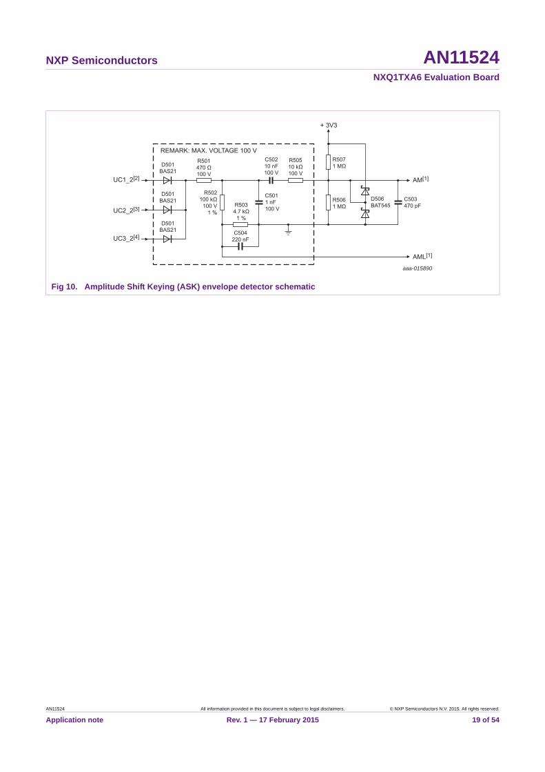
5.3 Amplitude-Shift Keying (ASK) envelope demodulator
One-directional communication from the mobile device to the base station is achieved via back-scattered Amplitude-Shift Keying modulation as illustrated in Figure 1.
The mobile device modulates the magnetic field of the base station using either capacitive or resistive load, at a rate of 2 kbits/sec.
An envelope detector is used to demodulate the communication data. The demodulated output is sent to the NXQ1TXA6 charging controller for further processing.
High voltages up to 100 Vp-p can be observed at the input of the envelope detector.
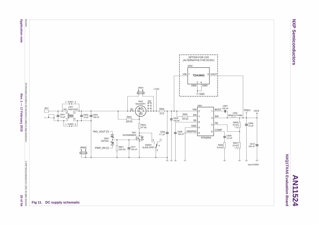
5.4 +12 V universal mains adapter
The power supply design is based on NXP TEA1720 low cost Switched Mode Power Supply (SMPS) controller IC. It is optimized for fly back converter topology to provide high-efficiency over the entire load range with ultra-low power consumption in the no-load condition.
AN11524 All information provided in this document is subject to legal disclaimers. © NXP Semiconductors N.V. 2015. All rights reserved.
Application note Rev. 1 — 17 February 2015 13 of 54
NXP Semiconductors AN11524NXQ1TXA6 Evaluation Board
5.5 Current measurement
The current flowing into the power stage is determined by measuring the voltage across a 22 m current sense resistor. The current measurement is needed for Foreign Object Detection (FOD). If FOD is not required, it can be disabled by configuring the resistor networks (refer to NXQ1TXA6 data sheet). The current measurement circuits can be removed. Connect the unused ISNS pin to ground, i.e. not left open. Note that FOD is required to pass Qi certification.
5.6 Bandgap reference voltage
NXQ1TXA6 wireless charging controller needs a band gap reference voltage (0.5 % tolerance) for critical processing. The TL431 shunt regulator is used in the NXQ1TXA6 Evaluation Board to provide this reference voltage.
5.7 DC-to-DC converter
A DC-to-DC buck converter steps the +12 V input down to +3.3 V, to supply the NXQ1TXA6 charging controller and other +3.3 V circuits.
A Richtek RT8295A DC-to-DC converter is used in the NXQ1TXA6 evaluation board. An option for a linear regulator TDA3663 is available on board. Take note however, that at operating currents of the NXQ1TXA6 evaluation board, the efficiency of the applied DC-to-DC converter is better than a linear regulator.
5.8 Near Field Communication (NFC) zero power in Standby mode
When using the optional feature "NFC tap to power on", the base station is designed for zero power consumption in standby mode. It uses an NT3H1201 NTAG-I2C NFC forum passive tag.
When this feature is enabled, there is no pinging to detect the presence of a mobile device on the charger pad. Instead, an NFC enabled mobile device, for example a phone, wakes up the base station via the NT3H1201. Power transfer takes place with a certified Qi mobile device.
To enable more functions such as Bluetooth pairing, smart advertisements, and connection handovers, the passive tag can be programmed with the NXP TagWriter application (see Section 3.9 “NFC functionality”).
AN11524 All information provided in this document is subject to legal disclaimers. © NXP Semiconductors N.V. 2015. All rights reserved.
Application note Rev. 1 — 17 February 2015 14 of 54
NXP Semiconductors AN11524NXQ1TXA6 Evaluation Board
6. Schematics and Bill Of Materials
Customers should start directly from NXQ1TXA6 Evaluation Board as this board is optimized in terms of functional performance and EMI.
Deviations are possible, but they should be kept minimal, carefully weighed and associated potential risks considered. Where possible, customers are encouraged to send their schematics to NXP for review. Contact the nearest NXP application support team in your area for support in designing your wireless charging base station.
During schematic capture, indicate critical components clearly in the schematics so that they are not forgotten during procurement and production. For example, 68 nF C0G/NP0 capacitor, 100 k 1 % tolerance resistor and 100 V rated components.
Certain critical components and PCB layout details are crucial to the success of the project and deserve special attention. In the later part of the document, these details are elaborated. Refer to Section 7 “Critical components”and Section 8 “PCB layout guidelines” in the subsequent pages.
For development of prototype boards, it is best practice to include test points on key signal nodes. For production runs, these test points can be removed from the final PCB.
At the very minimum, create test point for the following signal nodes:
• Power supplies - +3.3 V and +12 V supply nodes
• Output of ASK demodulator - AM signal node
• Output of current sense amplifier - ISOUT signal node
• Pulse Width Modulation - PWM signal node
• The half-bridge driver stage enable - nEN_HB1, 2 and 3 signal node
• System and power grounds - GND, GNDI
AN11524 All information provided in this document is subject to legal disclaimers. © NXP Semiconductors N.V. 2015. All rights reserved.
Application note Rev. 1 — 17 February 2015 15 of 54
xxxxxxxxxxxxxxxxxxxxx xxxxxxxxxxxxxxxxxxxxxxxxxx xxxxxxx x x x xxxxxxxxxxxxxxxxxxxxxxxxxxxxxx xxxxxxxxxxxxxxxxxxx xx xx xxxxx xxxxxxxxxxxxxxxxxxxxxxxxxxx xxxxxxxxxxxxxxxxxxx xxxxxx xxxxxxxxxxxxxxxxxxxxxxxxxxxxxxxxxxx xxxxxxxxxxxx x x xxxxxxxxxxxxxxxxxxxxx xxxxxxxxxxxxxxxxxxxxxxxxxxxxxx xxxxx xxxxxxxxxxxxxxxxxxxxxxxxxxxxxxxxxxxxxxxxxxxxxxxxxx xxxxxxxx xxxxxxxxxxxxxxxxxxxxxxxxx xxxxxxxxxxxxxxxxxxxx xxx
AN
11524
Ap
plicatio
n n
ote
NX
P S
emico
nd
ucto
rsA
N11524
NX
Q1
TX
A6
Ev
alu
ation
Bo
ard
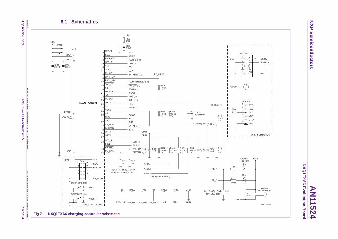
6.1 Schematics
aaa-015885
EXPIO1
+3V3 TESTIO
TESTCLK
SW1
BUZ
R11210 kΩ
BUZ101PS1240P02CT3
Ω
+3V3
+3V3R10247 kΩ
R107n.c.
9
7
5
3
1
10
8
6
4
2
TEST101
R101
n.c.
2
3
4
5
6RTSn
RXD
TXD
VCC
TXD
RXD
CTSn
UART101
1GND
+3V3
R109RED
GRNR111
1 kΩ
470 Ω
LED101LSG T676
ONLY FOR DEBUG
All inform
ation provided
in this docum
ent is subject to leg
al disclaim
ers.©
NX
P S
em
iconductors N
.V. 2015. A
ll rights reserved.
Rev. 1 —
17 Feb
ruary 2015
16 o
f 54
Fig 7. NXQ1TXA6 charging controller schematic
2RESET
3SEL3
8PWR_ON
9LED_G
10SCL
11SDA
15EN_HB1
16LP_VSUP
17PWM_HIN
18TAG_FD
19n.c.
21ISENSE
22ASK
23CL_DET
24NTC1
25n.c.
26VSNS
30SEL1
31RXD
32TXD
7EN_NFC
12BUZZER
20OPT0
27OPT1
28LED_R
1SEL2
13EN_HB2
14EN_HB3
SW1
ASEL3
PWR_ON [6]
LED_G
SCL
SDALP_VSUPEN_HB1 [1, 2]
IS- [2, 3, 4]
PWM_HIN [1, 2, 3, 4]
TAG_FD [7]
TESTCLK
ISOUT
AM [1, 5]
AML [1, 5]
NTC
TESTIO
measure power supply
R103100 kΩ1%
R104100 kΩ1 %
R10633.2 kΩ1 %
R11323.2 kΩ1 %
R11433.2 kΩ1 %
R105100 kΩ1%
U102TL431BFDT
C10410 nF
R11691 kΩ1 %
R115510 k1 %
ASEL1
RXD
TXD
EN_NFC [7]
BUZOPT1
ASEL1
ASEL2
ASEL3
OPT2
LED_R
ASEL2
EN_HB2 [1, 3]
EN_HB3 [1, 4]
U101
NXQ1TXA6/001
JP101
C102220 nF
C101220 nF
XTALIN
XTALOUT
VSS
4
5
VDD1
+3V3
6VDD2
29
33
C103220 nF
R119180 Ω1%
short R107 to GNDfor 1 LED option
short R117, R118 to GNDfor A6 1-coil base station
configuration setting
R117n.c.
R118n.c.
C10510 nF
C10610 nF
3
2
4
6
8
10
1
3
5
7
9SCL
SDA
EXPIO1
LP_VSUP
TP101
ONLY FOR DEBUG
SW101 B3FS-1000
SV101
SW14
1
2
3SW102 B3FS-1000
ASEL34
1
2
LED_R
LED_G
TP102 TP103 TP104 TP105 TP106 G101
GNDAMLAMEN_HB3EN_HB2EN_HB1PWM_HIN
xxxxxxxxxxxxxxxxxxxxx xxxxxxxxxxxxxxxxxxxxxxxxxx xxxxxxx x x x xxxxxxxxxxxxxxxxxxxxxxxxxxxxxx xxxxxxxxxxxxxxxxxxx xx xx xxxxx xxxxxxxxxxxxxxxxxxxxxxxxxxx xxxxxxxxxxxxxxxxxxx xxxxxx xxxxxxxxxxxxxxxxxxxxxxxxxxxxxxxxxxx xxxxxxxxxxxx x x xxxxxxxxxxxxxxxxxxxxx xxxxxxxxxxxxxxxxxxxxxxxxxxxxxx xxxxx xxxxxxxxxxxxxxxxxxxxxxxxxxxxxxxxxxxxxxxxxxxxxxxxxx xxxxxxxx xxxxxxxxxxxxxxxxxxxxxxxxx xxxxxxxxxxxxxxxxxxxx xxx
AN
11524
Ap
plicatio
n n
ote
NX
P S
emico
nd
ucto
rsA
N11524
NX
Q1
TX
A6
Ev
alu
ation
Bo
ard
aaa-015888
C21168 nF
G 100 V
C21068 nF
G 100 V
C217100 nF
C21622 μF
C214n.c.
C213n.c.
C1_2
GNDI GNDI GNDI GNDI
OUT
T+3 isth.
ISOUT[1]
TP203
5R202
2.2 kΩC21510 nF
3
4
OUT
T
U203*V+
IN+
IN-
6
All inform
ation provided
in this docum
ent is subject to leg
al disclaim
ers.©
NX
P S
em
iconductors N
.V. 2015. A
ll rights reserved.
Rev. 1 —
17 Feb
ruary 2015
17 o
f 54
Fig 8. Half bridge driver stage of coil 1 and current sense schematic
CO
CO
[5]U
COIL1CCOIL1T
CL1CCL1T1
2
3
4
GL
NWP2081
R205
R206
1 Ω
1 Ω
G201 G202
C207220 nF
SH
GH
FS
VDD
GND
SD
CLK
8
7
6
5
C203100 nF
C20110 nF
R20110 kΩ
C20622 μF1210
C218n.c.
GNDI
GNDI GNDI
GNDI
GNDI
GNDI GND
GNDI
GND
C205100 nF
T201NX3008NBKW
R203330 kΩ
[1, 3, 4]PWM_HIN
+12 V
[1]EN_HB1
GNDIGNDl
3
4
1
6
MAX44284HAU*only U202 or U20
mounted. Not bo
U202*
C202100 nF
R2040E022
1 %
RS+
RS-
VDD
SHDN
GND
C221100 nF
R210
U201
+3V3
n.c.
R207
Kelvin contacts
R208
10 Ω
10 Ω
NTC201
measuretemperature
LP_VSUP
NTC[1]
1
2
2
5
1
INA214AIDCK
REF
GND2
L1-1
C208n.c.
C209n.c.
R20922 kΩG
G
D
S
D
S
T203NX2020N2
T204NX2020N2
NODEBRIDGE
JP603
[1, 3, 4]IS-
xxxxxxxxxxxxxxxxxxxxx xxxxxxxxxxxxxxxxxxxxxxxxxx xxxxxxx x x x xxxxxxxxxxxxxxxxxxxxxxxxxxxxxx xxxxxxxxxxxxxxxxxxx xx xx xxxxx xxxxxxxxxxxxxxxxxxxxxxxxxxx xxxxxxxxxxxxxxxxxxx xxxxxx xxxxxxxxxxxxxxxxxxxxxxxxxxxxxxxxxxx xxxxxxxxxxxx x x xxxxxxxxxxxxxxxxxxxxx xxxxxxxxxxxxxxxxxxxxxxxxxxxxxx xxxxx xxxxxxxxxxxxxxxxxxxxxxxxxxxxxxxxxxxxxxxxxxxxxxxxxx xxxxxxxx xxxxxxxxxxxxxxxxxxxxxxxxx xxxxxxxxxxxxxxxxxxxx xxx
AN
11524
Ap
plicatio
n n
ote
NX
P S
emico
nd
ucto
rsA
N11524
NX
Q1
TX
A6
Ev
alu
ation
Bo
ard
aaa-015889
C30868 nF
G 100 V
C30768 nF
COG 100 VC312100 nF
C31122 μF
C3105.6 nFCOG 100 V
C3095.6 nFCOG 100 V
C2_2
1GL
R304
1 Ω
G301 G302
VDD8C303
GNDI GNDI GNDI GNDI
GNDI
+12 VU301
C305G
DT302NX2020N2
[1, 2, 4] IS-
C40868 nF
G 100 V
C40768 nF
G 100 VC412100 nF
C41122 μF
C410n.c.
C409n.c.
C3_2
G401 G402
GNDI GNDI GNDI GNDI
GNDI
All inform
ation provided
in this docum
ent is subject to leg
al disclaim
ers.©
NX
P S
em
iconductors N
.V. 2015. A
ll rights reserved.
Rev. 1 —
17 Feb
ruary 2015
18 o
f 54
Fig 9. Half bridge driver stage of coil 2 and 3
CO
[5] U
COIL2CCOIL2T
CL2CCL2T
2
3
4
NWP2081
R303
1 Ω
C304220 nF
SH
GH
FS
GND
SD
CLK
7
6
5
100 nF
GNDI GNDI
GNDI
GNDI
C302100 nF
T301NX3008NBKW
R302330 kΩ
[1, 2, 4] PWM_HIN
[1] EN_HB2
GNDIGNDl
L1-2
n.c.
C306n.c.
R30522 kΩG
S
D
ST303NX2020N2
JP605
CO
CO
[5] U
COIL3CCOIL3T
CL3CCL3T1
2
3
4
GL
NWP2081
R403
R404
1 Ω
1 Ω
C404220 nF
SH
GH
FS
VDD
GND
SD
CLK
8
7
6
5
C403100 nF
GNDI GNDI
GNDI
GNDI
C402100 nF
T401NX3008NBKW
R402330 kΩ
[1, 2, 3] PWM_HIN
+12 V
[1] EN_HB3
U401
L1-3
C405n.c.
C406n.c.
R40522 kΩG
G
D
S
D
S
T402NX2020N2
T403NX2020N2
[1, 2, 3] IS-
NXP Semiconductors AN11524NXQ1TXA6 Evaluation Board
Fig 10. Amplitude Shift Keying (ASK) envelope detector schematic
aaa-015890
UC1_2[2]
AML[1]
AM[1]
+ 3V3
REMARK: MAX. VOLTAGE 100 V
UC2_2[3]
UC3_2[4]
D501BAS21
R501470 Ω100 V
C50210 nF100 V
C504220 nF
C503470 pF
C5011 nF100 V
R502100 kΩ
100 V1 %
R5071 MΩ
R5061 MΩ
R50510 kΩ100 V
D501BAS21 D506
BAT545
D501BAS21
R5034.7 kΩ
1 %
AN11524 All information provided in this document is subject to legal disclaimers. © NXP Semiconductors N.V. 2015. All rights reserved.
Application note Rev. 1 — 17 February 2015 19 of 54
xxxxxxxxxxxxxxxxxxxxx xxxxxxxxxxxxxxxxxxxxxxxxxx xxxxxxx x x x xxxxxxxxxxxxxxxxxxxxxxxxxxxxxx xxxxxxxxxxxxxxxxxxx xx xx xxxxx xxxxxxxxxxxxxxxxxxxxxxxxxxx xxxxxxxxxxxxxxxxxxx xxxxxx xxxxxxxxxxxxxxxxxxxxxxxxxxxxxxxxxxx xxxxxxxxxxxx x x xxxxxxxxxxxxxxxxxxxxx xxxxxxxxxxxxxxxxxxxxxxxxxxxxxx xxxxx xxxxxxxxxxxxxxxxxxxxxxxxxxxxxxxxxxxxxxxxxxxxxxxxxx xxxxxxxx xxxxxxxxxxxxxxxxxxxxxxxxx xxxxxxxxxxxxxxxxxxxx xxx
AN
11524
Ap
plicatio
n n
ote
NX
P S
emico
nd
ucto
rsA
N11524
NX
Q1
TX
A6
Ev
alu
ation
Bo
ard
aaa-015891
BOOT TP601 +3V3
SW
FB
COMP
1
3
5
6
L602NR4012T100M
R60724 kΩ
1 %
R60875 kΩ
1 %
R6066.8 kΩ
C6083.3 nF
C60922 μF
C610100 nF
DC)
VOUT
C607100 nF
All inform
ation provided
in this docum
ent is subject to leg
al disclaim
ers.©
NX
P S
em
iconductors N
.V. 2015. A
ll rights reserved.
Rev. 1 —
17 Feb
ruary 2015
20 o
f 54 Fig 11. DC supply schematic
+12V
VIN2
7
8
4
9
EN
SS
GND
GNDPAD
1 2
1 2
J601
C60110 μF
SJ601
SJ602
3
4
2
1
C60210 μF
C603100 nF
L601WE_744273222
JP602
TAG_VOUT [7]
D
S
PWR_ON [1]
D601BAT54C
JP601
R602
220 kΩR60347 kΩ
R601220 kΩ
C611100 nF
T602NX2020P1
R604
22 Ω
100 kΩ
T601NX3008NBKW
SW601SLIDE-SPDT
C6044.7 μF
3 1
2
C605100 nF
C606100 nF
R605
OPTION FOR LDO(ALTERNATIVE FOR DC/
TDA3663
U602
1
2 4
3
GND
GND
GND
VIN
U601
RT8295A
NXP Semiconductors AN11524NXQ1TXA6 Evaluation Board
6.2 Bill Of Materials
The NXQ1TXA6 Evaluation Board is assembled with maximum options for evaluation purposes. For final design, certain components can be removed depending on the required features. The available options and corresponding components are presented below.
Options:
• Buzzer - only when buzzer is needed
• DCDC - when a DC-to-DC converter for 3.3 V is preferred
• LDO - when LDO regulator for 3.3 V is preferred
• NFC - when NFC is needed
• ZERO - when zero power standby is needed (also requires NFC)
• FOD - when FOD is required
• Debug - only for debugging, not for production
• NTC - only when NTC is needed
• NC - not connected, do not place
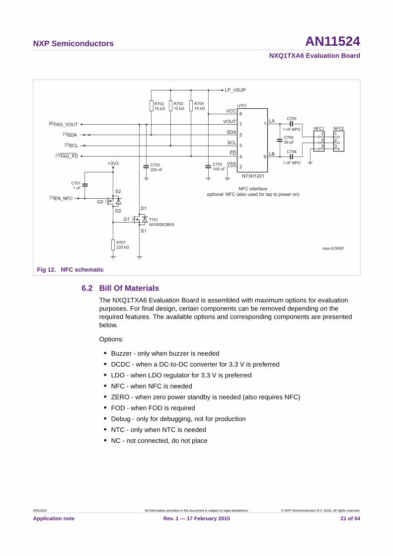
Fig 12. NFC schematic
aaa-015892
C7011 nF
R701220 kΩ
C702220 nF
R70210 kΩ
R70310 kΩ
R70410 kΩ
C703100 nF
C70439 pF
C705
C706
1 nF NPO
1 nF NPO
T701NX3008CBKS
[1]EN_NFC
[1]TAG_FD
[1]SCL
[1]SDA
[6]TAG_VOUT
+3V3
S2
D2 D1
S1
G1
G2
LP_VSUP
VCC
NFC interfaceoptional: NFC (also used for tap to power on)
VOUT LA
LB
SDA
SCL
FD
VSS
6
7
5
1
8
3
4
2
U701
NFC1
321
NFC2
321
NT3H1201
AN11524 All information provided in this document is subject to legal disclaimers. © NXP Semiconductors N.V. 2015. All rights reserved.
Application note Rev. 1 — 17 February 2015 21 of 54
xxxxxxxxxxxxxxxxxxxxx xxxxxxxxxxxxxxxxxxxxxxxxxx xxxxxxx x x x xxxxxxxxxxxxxxxxxxxxxxxxxxxxxx xxxxxxxxxxxxxxxxxxx xx xx xxxxx xxxxxxxxxxxxxxxxxxxxxxxxxxx xxxxxxxxxxxxxxxxxxx xxxxxx xxxxxxxxxxxxxxxxxxxxxxxxxxxxxxxxxxx xxxxxxxxxxxx x x xxxxxxxxxxxxxxxxxxxxx xxxxxxxxxxxxxxxxxxxxxxxxxxxxxx xxxxx xxxxxxxxxxxxxxxxxxxxxxxxxxxxxxxxxxxxxxxxxxxxxxxxxx xxxxxxxx xxxxxxxxxxxxxxxxxxxxxxxxx xxxxxxxxxxxxxxxxxxxx xxx
AN
11524
Ap
plicatio
n n
ote
NX
P S
emico
nd
ucto
rsA
N11524
NX
Q1
TX
A6
Ev
alu
ation
Bo
ard
Table 3. Bill Of Materials (BOM)
Part Value Part number Manufacturer Package Optional Description
BUZ101 PS1240P02CT3 PS1240P02CT3 TDK PS12 Buzzer audio indicator; round 12.2 mm 3.5 mm 4 kHz Vin = 3 V
capacitor, ceramic, 25 V, X7R, 20 %
capacitor, ceramic, 25 V, X7R, 20 %
capacitor, ceramic, 25 V, X7R, 20 %
capacitor, ceramic, 50 V, X7R, 10 %
capacitor, ceramic, 50 V, X7R, 10 %
capacitor, ceramic, 50 V, X7R, 10 %
capacitor, ceramic, 50 V, X7R, 10 %
capacitor, ceramic, 50 V, X7R, 10 %
capacitor, ceramic, 50 V, X7R, 10 %
capacitor, ceramic, 50 V, X7R, 10 %
capacitor, ceramic, 25 V, X7R, 10 %
capacitor, ceramic, 50 V, X7R, 10 %
capacitor, ceramic, 50 V, X7R, 10 %
capacitor, ceramic, 50 V, X7R, 10 %
capacitor, ceramic, 100 V, C0G, 5 %
capacitor, ceramic, 100 V, C0G, 5 %
capacitor, ceramic, 50 V, X7R, 10 %
capacitor, ceramic, 100 V, C0G, 5 %
capacitor, ceramic, 100 V, C0G, 5 %
capacitor, ceramic, 50 V, X7R, 10 %
capacitor, ceramic, 25 V, X7R, 10 %
capacitor, ceramic, 50 V, X7R, 10 %
capacitor, Polarized, Case_D, 25 V
capacitor, ceramic, 50 V, X7R, 10 %
capacitor, ceramic, 50 V, X7R, 10 %
capacitor, ceramic, 50 V, X7R, 10 %
capacitor, ceramic, 50 V, X7R, 10 %
capacitor, ceramic, 50 V, X7R, 10 %
capacitor, ceramic, 100 V, C0G, 5 %
All inform
ation provided
in this docum
ent is subject to leg
al disclaim
ers.©
NX
P S
em
iconductors N
.V. 2015. A
ll rights reserved.
Rev. 1 —
17 Feb
ruary 2015
22 o
f 54
C101 220 nF Standard - C0603 -
C102 220 nF Standard - C0603 -
C103 220 nF Standard - C0603 -
C104 10 nF Standard - C0603 -
C105 10 nF Standard - C0603 -
C106 10 nF Standard - C0603 -
C201 10 nF Standard - C0603 -
C202 100 nF Standard - C0603 FOD
C203 100 nF Standard - C0603 -
C205 100 nF Standard - C0603 -
C206 22F/1210 GRM32ER71E226KE15L MURATA C1210 -
C207 200 nF Standard - C0603 -
C208 n.c. Standard - C0603 n.c.
C209 n.c. Standard - C0603 n.c.
C210 68 nF/C0G/1812 C4532C0G2A683J250KA TDK C1812 -
C211 68 nF/C0G/1812 C4532C0G2A683J250KA TDK C1812 -
C212 100 nF Standard - C0603 FOD
C213 NC/100 V/C0G Standard - C1206 n.c.
C214 NC/100 V/C0G Standard - C1206 n.c.
C215 10 nF Standard - C0603 FOD
C216 22 F/1210 GRM32ER71E226KE15L MURATA C1210 -
C217 100 nF Standard - C0603 -
C218 NC/25V/Case_D Standard - SMC_D n.c.
C302 100 nF Standard - C0603 -
C303 100 nF Standard - C0603 -
C304 220 nF Standard - C0603 -
C305 n.c. Standard - C0603 n.c.
C306 n.c. Standard - C0603 n.c.
C307 68 nF/C0G/1812 C4532C0G2A683J250KA TDK C1812 -
xxxxxxxxxxxxxxxxxxxxx xxxxxxxxxxxxxxxxxxxxxxxxxx xxxxxxx x x x xxxxxxxxxxxxxxxxxxxxxxxxxxxxxx xxxxxxxxxxxxxxxxxxx xx xx xxxxx xxxxxxxxxxxxxxxxxxxxxxxxxxx xxxxxxxxxxxxxxxxxxx xxxxxx xxxxxxxxxxxxxxxxxxxxxxxxxxxxxxxxxxx xxxxxxxxxxxx x x xxxxxxxxxxxxxxxxxxxxx xxxxxxxxxxxxxxxxxxxxxxxxxxxxxx xxxxx xxxxxxxxxxxxxxxxxxxxxxxxxxxxxxxxxxxxxxxxxxxxxxxxxx xxxxxxxx xxxxxxxxxxxxxxxxxxxxxxxxx xxxxxxxxxxxxxxxxxxxx xxx
AN
11524
Ap
plicatio
n n
ote
NX
P S
emico
nd
ucto
rsA
N11524
NX
Q1
TX
A6
Ev
alu
ation
Bo
ard
C308 68 nF/C0G/1812 C4532C0G2A683J250KA TDK C1812 - capacitor, ceramic, 100 V, C0G, 5 %
C309 5.6 nF/C0G/1206 GCM3195C2A562JA16D MURATA C1206 - capacitor, ceramic, 100 V, C0G, 5 %
capacitor, ceramic, 100 V, C0G, 5 %
capacitor, ceramic, 25 V, X7R, 10 %
capacitor, ceramic, 25 V, X7R, 10 %
capacitor, ceramic, 25 V, X7R, 10 %
capacitor, ceramic, 50 V, X7R, 10 %
capacitor, ceramic, 50 V, X7R, 10 %
capacitor, ceramic, 50 V, X7R, 10 %
capacitor, ceramic, 50 V, X7R, 10 %
capacitor, ceramic, 100 V, C0G, 5 %
capacitor, ceramic, 100 V, C0G, 5 %
capacitor, ceramic, 100 V, C0G, 5 %
capacitor, ceramic, 100 V, C0G, 5 %
capacitor, ceramic, 25 V, X7R, 10 %
capacitor, ceramic, 50 V, X7R, 10 %
capacitor, ceramic, 100 V, X7R, 10 %
capacitor, ceramic, 100 V, X7R, 10 %
capacitor, ceramic, 50 V, X7R, 10 %
capacitor, ceramic, 50 V, X7R, 10 %
capacitor, ceramic, 25 V, X7R, 10 %
capacitor, ceramic, 25 V, X7R, 10 %
capacitor, ceramic, 50 V, X7R, 10 %
capacitor, ceramic, 25 V, X7R, 10 %
capacitor, ceramic, 50 V, X7R, 10 %
capacitor, ceramic, 50 V, X7R, 10 %
capacitor, ceramic, 50 V, X7R, 10 %
capacitor, ceramic, 50 V, X7R, 10 %
capacitor, ceramic, 6.3 V, X5R, 20 %
capacitor, ceramic, 50 V, X7R, 10 %
capacitor, ceramic, 50 V, X7R, 10 %
Table 3. Bill Of Materials (BOM) …continued
Part Value Part number Manufacturer Package Optional Description
All inform
ation provided
in this docum
ent is subject to leg
al disclaim
ers.©
NX
P S
em
iconductors N
.V. 2015. A
ll rights reserved.
Rev. 1 —
17 Feb
ruary 2015
23 o
f 54
C310 5.6 nF/C0G/1206 GCM3195C2A562JA16D MURATA C1206 -
C311 22 F/1210 GRM32ER71E226KE15L MURATA C1210 -
C312 100 nF Standard - C0603 -
C402 100 nF Standard - C0603 -
C403 100 nF Standard - C0603 -
C404 220 nF Standard - C0603 -
C405 n.c. Standard - C0603 n.c.
C406 n.c. Standard - C0603 n.c.
C407 68 nF/C0G/1812 C4532C0G2A683J250KA TDK C1812 -
C408 68 nF/C0G/1812 C4532C0G2A683J250KA TDK C1812 -
C409 NC/100V/C0G Standard - C1206 n.c.
C410 NC/100V/C0G Standard - C1206 n.c.
C411 22 F/1210 GRM32ER71E226KE15L MURATA C1210 -
C412 100 nF Standard - C0603 -
C501 1 nF/1206 Standard - C1206 -
C502 10 nF/1206 Standard - C1206 -
C503 470 pF Standard - C0603 -
C504 220 nF Standard - C0603 -
C601 10 F/1206 Standard - C1206 -
C602 10 F/1206 Standard - C1206 -
C603 100 nF Standard - C0603 -
C604 4.7 F/0805 GRM21BR71E475KA73L MURATA C0805 -
C605 100 nF Standard - C0603 -
C606 100 nF Standard - C0603 DCDC
C607 100 nF Standard - C0603 DCDC
C608 3.3 nF Standard - C0603 DCDC
C609 22 F/0805 GRM21BR60J226ME39L MURATA C0805 -
C610 100 nF Standard - C0603 -
C611 100 nF Standard - C0603 ZERO
xxxxxxxxxxxxxxxxxxxxx xxxxxxxxxxxxxxxxxxxxxxxxxx xxxxxxx x x x xxxxxxxxxxxxxxxxxxxxxxxxxxxxxx xxxxxxxxxxxxxxxxxxx xx xx xxxxx xxxxxxxxxxxxxxxxxxxxxxxxxxx xxxxxxxxxxxxxxxxxxx xxxxxx xxxxxxxxxxxxxxxxxxxxxxxxxxxxxxxxxxx xxxxxxxxxxxx x x xxxxxxxxxxxxxxxxxxxxx xxxxxxxxxxxxxxxxxxxxxxxxxxxxxx xxxxx xxxxxxxxxxxxxxxxxxxxxxxxxxxxxxxxxxxxxxxxxxxxxxxxxx xxxxxxxx xxxxxxxxxxxxxxxxxxxxxxxxx xxxxxxxxxxxxxxxxxxxx xxx
AN
11524
Ap
plicatio
n n
ote
NX
P S
emico
nd
ucto
rsA
N11524
NX
Q1
TX
A6
Ev
alu
ation
Bo
ard
C701 1 nF Standard - C0603 NFC capacitor, ceramic, 50 V, X7R, 10 %
C702 220 nF Standard - C0603 NFC capacitor, ceramic, 50 V, X7R, 10 %
capacitor, ceramic, 50 V, X7R, 10 %
capacitor, ceramic, 50 V, NP0, 5 %
capacitor, ceramic, 50 V, NP0, 5 %
capacitor, ceramic, 50 V, NP0, 5 %
High-voltage switching diode
High-voltage switching diode
High-voltage switching diode
Schottky barrier double diodes
Schottky barrier double diodes
DC10A - Socket PCB, DC Power, 2.49 mm
header, pin, 2.54 mm, 2 way 1 row
header, pin, 2.54 mm, 2 way 1 row
header, pin, 2.54 mm, 2 way 1 row
Line filter, CMODE, 30 H, 2.2 k 25 %
Inductor, shielded 10 H, 740 mA, SMD
Coil Module - TX (A6) 12.5 H/11.5 H
Standard LEDs - SMD Red/Green
NFC-Antenna
thermistor, NTC, Radial leaded
chip resistor, 0.1 W, 5 %
chip resistor, 0.1 W, 5 %
chip resistor, 0.1 W, 1 %
chip resistor, 0.1 W, 1 %
chip resistor, 0.1 W, 1 %
chip resistor, 0.1 W, 1 %
chip resistor, 0.1 W, 5 %
Table 3. Bill Of Materials (BOM) …continued
Part Value Part number Manufacturer Package Optional Description
All inform
ation provided
in this docum
ent is subject to leg
al disclaim
ers.©
NX
P S
em
iconductors N
.V. 2015. A
ll rights reserved.
Rev. 1 —
17 Feb
ruary 2015
24 o
f 54
C703 100 nF Standard - C0603 NFC
C704 39 pF/NP0 Standard - C0603 NFC
C705 1nF/NP0 Standard - C0603 NFC
C706 1nF/NP0 Standard - C0603 NFC
D501 BAS21 BAS21 NXP Semiconductors SOT23 -
D502 BAS21 BAS21 NXP Semiconductors SOT23 -
D503 BAS21 BAS21 NXP Semiconductors SOT23 -
D506 BAT54S BAT54S NXP Semiconductors SOT23 -
D601 BAT54C BAT54C NXP Semiconductors SOT23 ZERO
J601 DC10A DC10A CLIFF Electronic DC10 -
Components
JP101 JP1E Standard - JP1 Debug
JP601 JP1E Standard - JP1 Debug
JP602 JP1E Standard - JP1 Debug
L601 30 H, 2.2 k 744273222 Würth Elektronik WE-SL5_HC -
L602 NR4012T100M NR4012T100M TAIYO YUDEN NR4012 DCDC
L1 Y31-60037F Y31-60037F Elec & Eltek Magnetic
Y31-60037F -
LED101 LSG T676 LSG T676-P7Q7-1+N7P7-24 OSRAM PLCC-4 -
NFC1 NFC-Antenna NFC-Antenna - NFC NFC
NTC201 B57551G1103F005 B57551G1103F005 EPCOS - NTC
R101 n.c. Standard - R0603 n.c.
R102 47 k Standard - R0603 -
R103 100 k /1 % Standard - R0603 -
R104 100 k /1 % Standard - R0603 -
R105 100 k /1 % Standard - R0603 -
R106 33.2 k /1 % Standard - R0603 -
R107 n.c. Standard - R0603 n.c.
xxxxxxxxxxxxxxxxxxxxx xxxxxxxxxxxxxxxxxxxxxxxxxx xxxxxxx x x x xxxxxxxxxxxxxxxxxxxxxxxxxxxxxx xxxxxxxxxxxxxxxxxxx xx xx xxxxx xxxxxxxxxxxxxxxxxxxxxxxxxxx xxxxxxxxxxxxxxxxxxx xxxxxx xxxxxxxxxxxxxxxxxxxxxxxxxxxxxxxxxxx xxxxxxxxxxxx x x xxxxxxxxxxxxxxxxxxxxx xxxxxxxxxxxxxxxxxxxxxxxxxxxxxx xxxxx xxxxxxxxxxxxxxxxxxxxxxxxxxxxxxxxxxxxxxxxxxxxxxxxxx xxxxxxxx xxxxxxxxxxxxxxxxxxxxxxxxx xxxxxxxxxxxxxxxxxxxx xxx
AN
11524
Ap
plicatio
n n
ote
NX
P S
emico
nd
ucto
rsA
N11524
NX
Q1
TX
A6
Ev
alu
ation
Bo
ard
R109 1 k Standard - R0603 - chip resistor, 0.1 W, 5 %
R111 470 R Standard - R0603 - chip resistor, 0.1 W, 5 %
chip resistor, 0.1 W, 5 %
chip resistor, 0.1 W, 1 %
chip resistor, 0.1 W, 1 %
chip resistor, 0.1 W, 1 %
chip resistor, 0.1 W, 1 %
chip resistor, 0.1 W, 5 %
chip resistor, 0.1 W, 5 %
chip resistor, 0.1 W, 1 %
chip resistor, 0.1 W, 5 %
chip resistor, 0.1 W, 5 %
chip resistor, 0.1 W, 5 %
chip resistor, 0.1 W, 1 %
chip resistor, 0.1 W, 5 %
chip resistor, 0.1 W, 5 %
chip resistor, 0.1 W, 5 %
chip resistor, 0.1 W, 5 %
chip resistor, 0.1 W, 5 %
chip resistor, 0.1 W, 5 %
chip resistor, 0.1 W, 5 %
chip resistor, 0.1 W, 5 %
chip resistor, 0.1 W, 5 %
chip resistor, 0.1 W, 5 %
chip resistor, 0.1 W, 5 %
chip resistor, 0.1 W, 5 %
chip resistor, 0.1 W, 5 %
chip resistor, 0.1 W, 5 %
chip resistor, 0.25 W, 5 %
chip resistor, 0.25 W, 1 %
chip resistor, 0.1 W, 1 %
Table 3. Bill Of Materials (BOM) …continued
Part Value Part number Manufacturer Package Optional Description
All inform
ation provided
in this docum
ent is subject to leg
al disclaim
ers.©
NX
P S
em
iconductors N
.V. 2015. A
ll rights reserved.
Rev. 1 —
17 Feb
ruary 2015
25 o
f 54
R112 10 k Standard - R0603 Buzzer
R113 23.2 k /1 % Standard - R0603 -
R114 33.2 k /1 % Standard - R0603 -
R115 510 k /1 % Standard - R0603 -
R116 91 k /1 % Standard - R0603 -
R117 n.c. Standard - R0603 n.c.
R118 n.c. Standard - R0603 n.c.
R119 180 R / 1 % Standard - R0603 -
R201 10 k Standard - R0603 -
R202 2.2 k Standard - R0603 FOD
R203 330 k Standard - R0603 -
R204 0E022/1 % WSLP0805R0220FEA VISHAY R0805 FOD
R205 1 R Standard - R0603 -
R206 1 R Standard - R0603 -
R207 10 R Standard - R0603 FOD
R208 10 R Standard - R0603 FOD
R209 22 k RES0603 - R0603 -
R210 n.c. Standard - R0603 n.c.
R302 330 k Standard R0603 -
R303 1 R Standard R0603 -
R304 1 R Standard R0603 -
R305 22 k Standard R0603 -
R402 330 k Standard R0603 -
R403 1 R Standard R0603 -
R404 1 R Standard R0603 -
R405 22 k Standard R0603 -
R501 470R/100 V Standard R1206 -
R502 100 k/100 V/1 % Standard R1206 -
R503 4.7 k/1 % Standard R0603 -
xxxxxxxxxxxxxxxxxxxxx xxxxxxxxxxxxxxxxxxxxxxxxxx xxxxxxx x x x xxxxxxxxxxxxxxxxxxxxxxxxxxxxxx xxxxxxxxxxxxxxxxxxx xx xx xxxxx xxxxxxxxxxxxxxxxxxxxxxxxxxx xxxxxxxxxxxxxxxxxxx xxxxxx xxxxxxxxxxxxxxxxxxxxxxxxxxxxxxxxxxx xxxxxxxxxxxx x x xxxxxxxxxxxxxxxxxxxxx xxxxxxxxxxxxxxxxxxxxxxxxxxxxxx xxxxx xxxxxxxxxxxxxxxxxxxxxxxxxxxxxxxxxxxxxxxxxxxxxxxxxx xxxxxxxx xxxxxxxxxxxxxxxxxxxxxxxxx xxxxxxxxxxxxxxxxxxxx xxx
AN
11524
Ap
plicatio
n n
ote
NX
P S
emico
nd
ucto
rsA
N11524
NX
Q1
TX
A6
Ev
alu
ation
Bo
ard
R505 10 k/100 V Standard R1206 - chip resistor, 0.25 W, 5 %
R506 1M0 Standard R0603 - chip resistor, 0.1 W, 5 %
chip resistor, 0.1 W, 5 %
chip resistor, 0.1 W, 5 %
chip resistor, 0.1 W, 5 %
chip resistor, 0.1 W, 5 %
chip resistor, 0.125 W, 5 %
chip resistor, 0.1 W, 5 %
chip resistor, 0.1 W, 5 %
chip resistor, 0.1 W, 1 %
chip resistor, 0.1 W, 1 %
chip resistor, 0.1 W, 5 %
chip resistor, 0.1 W, 5 %
chip resistor, 0.1 W, 5 %
chip resistor, 0.1 W, 5 %
header, pin, 2.54 mm, 10 way, 2 row
B3FS-1000 - switch, flat, SPNO
B3FS-1000 - switch, flat, SPNO
OS102011MA1QN1 - switch, SPDT, 0.1 A, 12 V, PCB, R/A
30 V, 350 mA N-channel Trench MOSFET
30 V N-channel Trench MOSFET
30 V N-channel Trench MOSFET
30 V, 350 mA N-channel Trench MOSFET
30 V N-channel Trench MOSFET
30 V N-channel Trench MOSFET
30 V, 350 mA N-channel Trench MOSFET
Table 3. Bill Of Materials (BOM) …continued
Part Value Part number Manufacturer Package Optional Description
All inform
ation provided
in this docum
ent is subject to leg
al disclaim
ers.©
NX
P S
em
iconductors N
.V. 2015. A
ll rights reserved.
Rev. 1 —
17 Feb
ruary 2015
26 o
f 54
R507 1M0 Standard R0603 -
R601 220 k Standard R0603 ZERO
R602 220 k Standard R0603 ZERO
R603 47 k Standard R0603 ZERO
R604 22 R Standard R0805 -
R605 100 k Standard R0603 DCDC
R606 6.8 k Standard R0603 DCDC
R607 24 k /1 % Standard - R0603 DCDC
R608 75 k /1 % Standard - R0603 DCDC
R701 220 k Standard - R0603 NFC
R702 10 k Standard - R0603 NFC
R703 10 k Standard - R0603 NFC
R704 10 k Standard - R0603 NFC
SV101 MA05-2 Standard - MA05-2 Debug
SW101 B3FS-1000 B3FS-1000 Omron Electronic Components
SWITCHTACT_ DTSM-6
Debug
SW102 B3FS-1000 B3FS-1000 Omron Electronic Components
SWITCHTACT_ DTSM-6
Debug
SW601 SLIDE-SPDT SLIDE-SPDT C&K Components SLIDE-SPDT ZERO
T201 NX3008NBKW NX3008NBKW NXP Semiconductors SOT323 -
T203 NX2020N2 NX2020N2 NXP Semiconductors SOT1220 -
T204 NX2020N2 NX2020N2 NXP Semiconductors SOT1220 -
T301 NX3008NBKW NX3008NBKW NXP Semiconductors SOT323 -
T302 NX2020N2 NX2020N2 NXP Semiconductors SOT1220 -
T303 NX2020N2 NX2020N2 NXP Semiconductors SOT1220 -
T401 NX3008NBKW NX3008NBKW NXP Semiconductors SOT323 -
xxxxxxxxxxxxxxxxxxxxx xxxxxxxxxxxxxxxxxxxxxxxxxx xxxxxxx x x x xxxxxxxxxxxxxxxxxxxxxxxxxxxxxx xxxxxxxxxxxxxxxxxxx xx xx xxxxx xxxxxxxxxxxxxxxxxxxxxxxxxxx xxxxxxxxxxxxxxxxxxx xxxxxx xxxxxxxxxxxxxxxxxxxxxxxxxxxxxxxxxxx xxxxxxxxxxxx x x xxxxxxxxxxxxxxxxxxxxx xxxxxxxxxxxxxxxxxxxxxxxxxxxxxx xxxxx xxxxxxxxxxxxxxxxxxxxxxxxxxxxxxxxxxxxxxxxxxxxxxxxxx xxxxxxxx xxxxxxxxxxxxxxxxxxxxxxxxx xxxxxxxxxxxxxxxxxxxx xxx
AN
11524
Ap
plicatio
n n
ote
NX
P S
emico
nd
ucto
rsA
N11524
NX
Q1
TX
A6
Ev
alu
ation
Bo
ard
T402 NX2020N2 NX2020N2 NXP Semiconductors SOT1220 - 30 V N-channel Trench MOSFET
T403 NX2020N2 NX2020N2 NXP Semiconductors SOT1220 - 30 V N-channel Trench MOSFET
30 V, 350 mA N-channel Trench MOSFET
30 V, single P-channel Trench MOSFET
30/30 V, 350/250 mA N/P-channel Trench MOSFET
connector header, SMT, R/A, 1.27 mm, 10P
Qi-compliant charging controller
VREG, 0.5 %, 2.495 V, 36 V
Half bridge driver IC
High precision, low-power current-sense amplifier
voltage output, current-shunt monitor
Half bridge driver IC
Half bridge driver IC
2 A, 23 V, 340 kHz synchronous step-down converter
3.3 V voltage regulator
NFC Forum type 2 Tag compliant IC with IC interface
header, pin, 2.54 mm, 6 way, 1 row
Table 3. Bill Of Materials (BOM) …continued
Part Value Part number Manufacturer Package Optional Description
All inform
ation provided
in this docum
ent is subject to leg
al disclaim
ers.©
NX
P S
em
iconductors N
.V. 2015. A
ll rights reserved.
Rev. 1 —
17 Feb
ruary 2015
27 o
f 54
T601 NX3008NBKW NX3008NBKW NXP Semiconductors SOT323 ZERO
T602 NX2020P1 NX2020P1 NXP Semiconductors SOT1220 ZERO
T701 NX3008CBKS NX3008CBKS NXP Semiconductors SOT363 NFC
TEST101 M50-3600542 M50-3600542 Samtec 127_2R10_SMT Debug
U101 NXQ1TXA6 NXQ1TXA6/001 NXP Semiconductors SOT865 -
U102 TL431BFDT TL431BFDT NXP Semiconductors SOT23 -
U201 NWP2081T NWP2081T NXP Semiconductors SOT96 -
U202 MAX44284HAUT+ MAX44284HAUT+ Maxim Integrated SOT457 FOD
U203 n.c. INA214AIDCKT Texas Instruments SC70 n.c.
U301 NWP2081T NWP2081T NXP Semiconductors SOT96 -
U401 NWP2081T NWP2081T NXP Semiconductors SOT96 -
U601 RT8295A RT8295A Richtek SOP-8 DCDC
U602 TDA3663 TDA3663 NXP Semiconductors SOT223 LDO
U701 NT3H1201 NT3H1201W0FHK NXP Semiconductors SOT902 NFC
UART101 MA06-1 Standard - MA06-1 Debug
NXP Semiconductors AN11524NXQ1TXA6 Evaluation Board
7. Critical components
As mentioned in Section 6, certain components are critical in the design. In this section, we discuss these components, associated design considerations and potential pitfalls.
7.1 Power stage
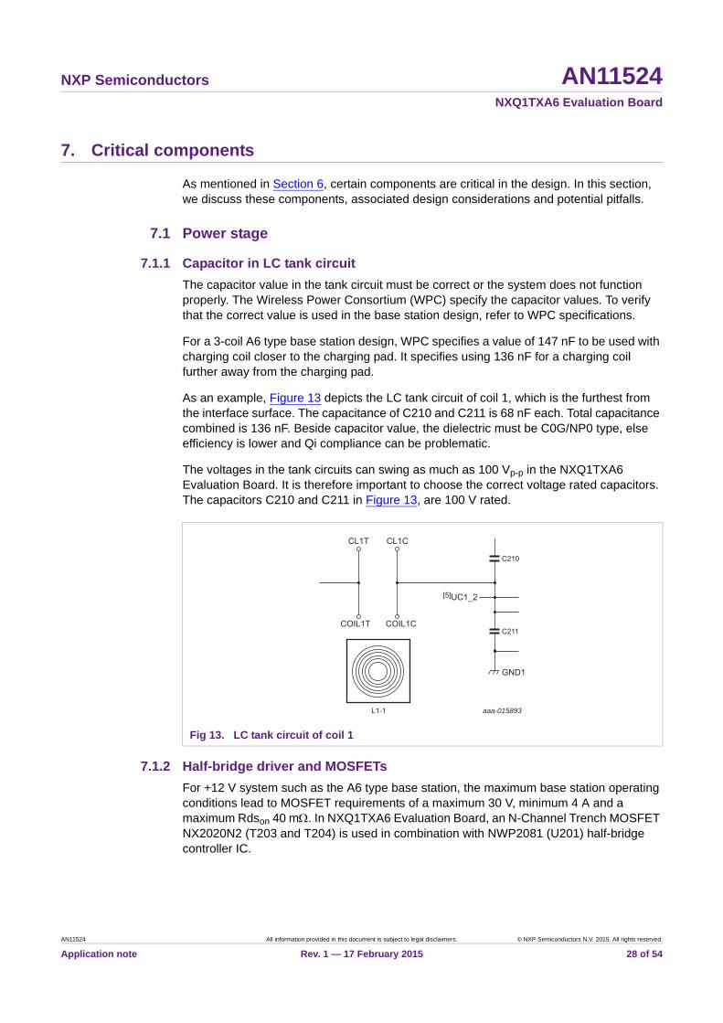
7.1.1 Capacitor in LC tank circuit
The capacitor value in the tank circuit must be correct or the system does not function properly. The Wireless Power Consortium (WPC) specify the capacitor values. To verify that the correct value is used in the base station design, refer to WPC specifications.
For a 3-coil A6 type base station design, WPC specifies a value of 147 nF to be used with charging coil closer to the charging pad. It specifies using 136 nF for a charging coil further away from the charging pad.
As an example, Figure 13 depicts the LC tank circuit of coil 1, which is the furthest from the interface surface. The capacitance of C210 and C211 is 68 nF each. Total capacitance combined is 136 nF. Beside capacitor value, the dielectric must be C0G/NP0 type, else efficiency is lower and Qi compliance can be problematic.
The voltages in the tank circuits can swing as much as 100 Vp-p in the NXQ1TXA6 Evaluation Board. It is therefore important to choose the correct voltage rated capacitors. The capacitors C210 and C211 in Figure 13, are 100 V rated.
7.1.2 Half-bridge driver and MOSFETs
For +12 V system such as the A6 type base station, the maximum base station operating conditions lead to MOSFET requirements of a maximum 30 V, minimum 4 A and a maximum Rdson 40 m. In NXQ1TXA6 Evaluation Board, an N-Channel Trench MOSFET NX2020N2 (T203 and T204) is used in combination with NWP2081 (U201) half-bridge controller IC.
Fig 13. LC tank circuit of coil 1
aaa-015893
C211
GND1
C210
L1-1
[5]UC1_2
COIL1CCOIL1T
CL1CCL1T
AN11524 All information provided in this document is subject to legal disclaimers. © NXP Semiconductors N.V. 2015. All rights reserved.
Application note Rev. 1 — 17 February 2015 28 of 54
NXP Semiconductors AN11524NXQ1TXA6 Evaluation Board
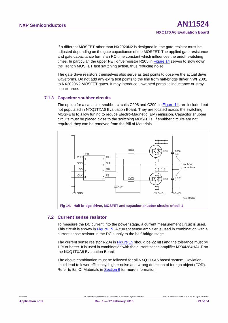
If a different MOSFET other than NX2020N2 is designed in, the gate resistor must be adjusted depending on the gate capacitance of the MOSFET. The applied gate resistance and gate capacitance forms an RC time constant which influences the on/off switching times. In particular, the upper FET drive resistor R205 in Figure 14 serves to slow down the Trench MOSFET fast switching action, thus reducing noise.
The gate drive resistors themselves also serve as test points to observe the actual drive waveforms. Do not add any extra test points to the line from half-bridge driver NWP2081 to NX2020N2 MOSFET gates. It may introduce unwanted parasitic inductance or stray capacitance.
7.1.3 Capacitor snubber circuits
The option for a capacitor snubber circuits C208 and C209, in Figure 14, are included but not populated in NXQ1TXA6 Evaluation Board. They are located across the switching MOSFETs to allow tuning to reduce Electro-Magnetic (EM) emission. Capacitor snubber circuits must be placed close to the switching MOSFETs. If snubber circuits are not required, they can be removed from the Bill of Materials.
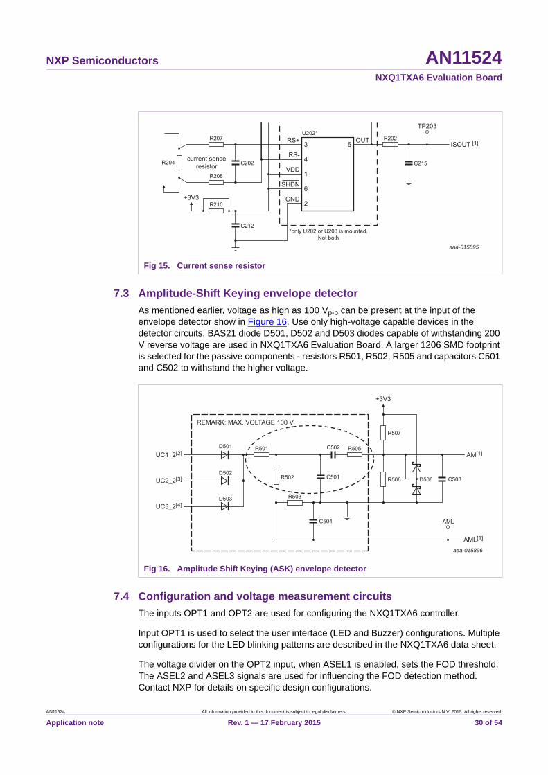
7.2 Current sense resistor
To measure the DC current into the power stage, a current measurement circuit is used. This circuit is shown in Figure 15. A current sense amplifier is used in combination with a current sense resistor in the DC supply to the half-bridge stage.
The current sense resistor R204 in Figure 15 should be 22 m and the tolerance must be 1 % or better. It is used in combination with the current sense amplifier MX44284HAUT on the NXQ1TXA6 Evaluation Board.
The above combination must be followed for all NXQ1TXA6 based system. Deviation could lead to lower efficiency, higher noise and wrong detection of foreign object (FOD). Refer to Bill Of Materials in Section 6 for more information.
Fig 14. Half bridge driver, MOSFET and capacitor snubber circuits of coil 1
aaa-015894
C208n.c.
C209n.c.
1
2
3
4
GLU201
R205
R206
C207
SH
GH
FS
VDD
GND
SD
CLK
8
7
6
5
T203
T204
GNDIGNDI GNDI
snubbercapacitors
AN11524 All information provided in this document is subject to legal disclaimers. © NXP Semiconductors N.V. 2015. All rights reserved.
Application note Rev. 1 — 17 February 2015 29 of 54
NXP Semiconductors AN11524NXQ1TXA6 Evaluation Board
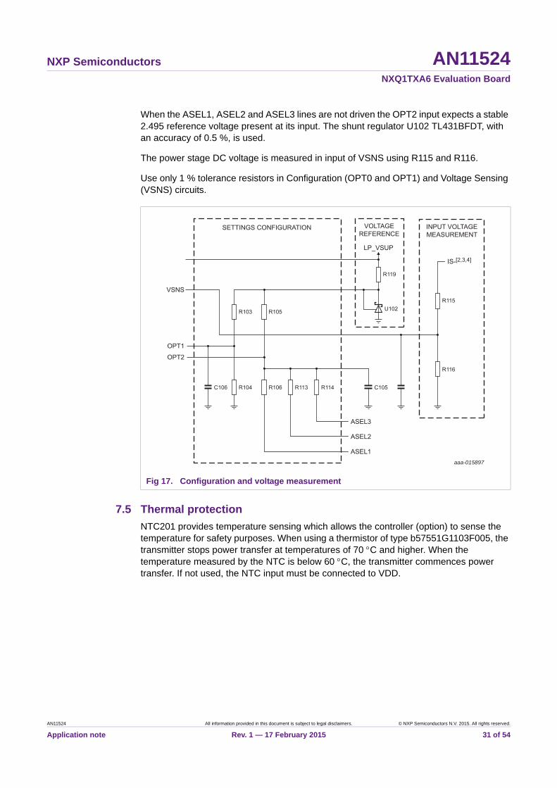
7.3 Amplitude-Shift Keying envelope detector
As mentioned earlier, voltage as high as 100 Vp-p can be present at the input of the envelope detector show in Figure 16. Use only high-voltage capable devices in the detector circuits. BAS21 diode D501, D502 and D503 diodes capable of withstanding 200 V reverse voltage are used in NXQ1TXA6 Evaluation Board. A larger 1206 SMD footprint is selected for the passive components - resistors R501, R502, R505 and capacitors C501 and C502 to withstand the higher voltage.
7.4 Configuration and voltage measurement circuits
The inputs OPT1 and OPT2 are used for configuring the NXQ1TXA6 controller.
Input OPT1 is used to select the user interface (LED and Buzzer) configurations. Multiple configurations for the LED blinking patterns are described in the NXQ1TXA6 data sheet.
The voltage divider on the OPT2 input, when ASEL1 is enabled, sets the FOD threshold. The ASEL2 and ASEL3 signals are used for influencing the FOD detection method. Contact NXP for details on specific design configurations.
Fig 15. Current sense resistor
3
4
1
6
OUTISOUT [1]
TP203U202*
*only U202 or U203 is mounted.Not both
C202R204
RS+
RS-
VDD
SHDN
2GND
5
C212
R202
C215
aaa-015895
R207
R210
current senseresistor
+3V3
R208
Fig 16. Amplitude Shift Keying (ASK) envelope detector
aaa-015896
D501
D502
D503
D506
UC1_2[2]
UC2_2[3]
UC3_2[4]
AM[1]
REMARK: MAX. VOLTAGE 100 V
+3V3
R501
R502 C501
C502
C504
R503
R505
R506
R507
C503
AML[1]
AML
AN11524 All information provided in this document is subject to legal disclaimers. © NXP Semiconductors N.V. 2015. All rights reserved.
Application note Rev. 1 — 17 February 2015 30 of 54
NXP Semiconductors AN11524NXQ1TXA6 Evaluation Board
When the ASEL1, ASEL2 and ASEL3 lines are not driven the OPT2 input expects a stable 2.495 reference voltage present at its input. The shunt regulator U102 TL431BFDT, with an accuracy of 0.5 %, is used.
The power stage DC voltage is measured in input of VSNS using R115 and R116.
Use only 1 % tolerance resistors in Configuration (OPT0 and OPT1) and Voltage Sensing (VSNS) circuits.
7.5 Thermal protection
NTC201 provides temperature sensing which allows the controller (option) to sense the temperature for safety purposes. When using a thermistor of type b57551G1103F005, the transmitter stops power transfer at temperatures of 70 C and higher. When the temperature measured by the NTC is below 60 C, the transmitter commences power transfer. If not used, the NTC input must be connected to VDD.
Fig 17. Configuration and voltage measurement
aaa-015897
IS-[2,3,4]
INPUT VOLTAGEMEASUREMENT
VOLTAGEREFERENCE
SETTINGS CONFIGURATION
LP_VSUP
VSNS
R103
R104 R106 R113 R114
R105
R116
R115
OPT1
ASEL3
ASEL2
ASEL1
OPT2
R119
U102
C106 C105
AN11524 All information provided in this document is subject to legal disclaimers. © NXP Semiconductors N.V. 2015. All rights reserved.
Application note Rev. 1 — 17 February 2015 31 of 54
NXP Semiconductors AN11524NXQ1TXA6 Evaluation Board
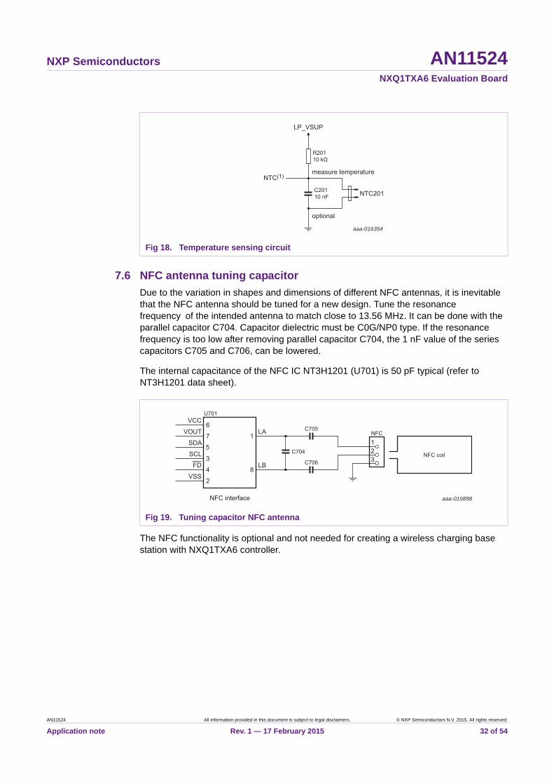
7.6 NFC antenna tuning capacitor
Due to the variation in shapes and dimensions of different NFC antennas, it is inevitable that the NFC antenna should be tuned for a new design. Tune the resonance frequency of the intended antenna to match close to 13.56 MHz. It can be done with the parallel capacitor C704. Capacitor dielectric must be C0G/NP0 type. If the resonance frequency is too low after removing parallel capacitor C704, the 1 nF value of the series capacitors C705 and C706, can be lowered.
The internal capacitance of the NFC IC NT3H1201 (U701) is 50 pF typical (refer to NT3H1201 data sheet).
The NFC functionality is optional and not needed for creating a wireless charging base station with NXQ1TXA6 controller.
Fig 18. Temperature sensing circuit
aaa-016354
C20110 nF NTC201
R20110 kΩ
measure temperature
optional
NTC(1)
LP_VSUP
Fig 19. Tuning capacitor NFC antenna
aaa-015898
C704
C705NFC
NFC coilC706 3
21
6
7
5
3
LA
U701VCC
NFC interface
VOUT
SDA
SCL
4FD
2VSS
1
LB8
AN11524 All information provided in this document is subject to legal disclaimers. © NXP Semiconductors N.V. 2015. All rights reserved.
Application note Rev. 1 — 17 February 2015 32 of 54
NXP Semiconductors AN11524NXQ1TXA6 Evaluation Board
8. PCB layout guidelines
Having a proper printed circuit board (PCB) layout is critical to the success of the application. A poor constructed PCB layout can cause the whole application not to function properly. Beyond basic circuit operation, it can also directly influence the ElectroMagnetic Compatibility (EMC) profile. Therefore, it is imperative that care should be exercised during the PCB layout stage.
Several good PCB design tips are explained here.
8.1 Ground planes
Design with a 4-layer PCB. The layer stack-up applied in NXQ1TXA6 Evaluation Board is as follows:
1. Layer 1: Component placement and signal trace
2. Layer 2: Clean uninterrupted ground
3. Layer 3: Signal trace
4. Layer 4: Ground and minimal routing trace if required
Notice that with this stacking technique, the signal traces are sandwiched between grounds. It provides a solid ground reference plane and helps to minimize ElectroMagnetic Interference (EMI) noise emissions.
As a rule, use ground planes: use copper-pour in unused areas of the PCB and stitch these areas with vias to inner ground planes.
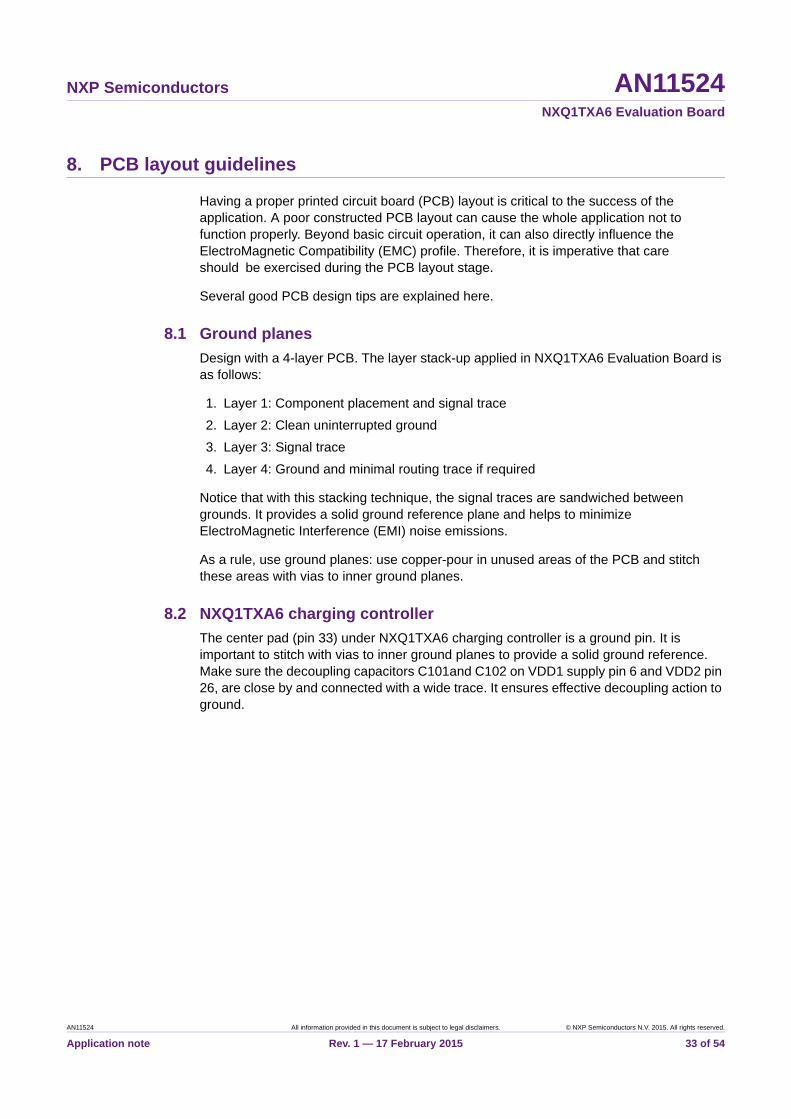
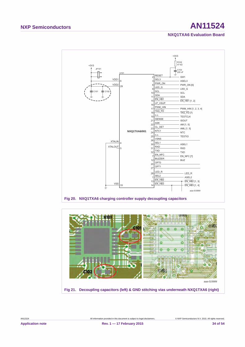
8.2 NXQ1TXA6 charging controller
The center pad (pin 33) under NXQ1TXA6 charging controller is a ground pin. It is important to stitch with vias to inner ground planes to provide a solid ground reference. Make sure the decoupling capacitors C101and C102 on VDD1 supply pin 6 and VDD2 pin 26, are close by and connected with a wide trace. It ensures effective decoupling action to ground.
AN11524 All information provided in this document is subject to legal disclaimers. © NXP Semiconductors N.V. 2015. All rights reserved.
Application note Rev. 1 — 17 February 2015 33 of 54
NXP Semiconductors AN11524NXQ1TXA6 Evaluation Board
Fig 20. NXQ1TXA6 charging controller supply decoupling capacitors
Fig 21. Decoupling capacitors (left) & GND stitching vias underneath NXQ1TXA6 (right)
aaa-015899
2RESET
3SEL3
8PWR_ON
9LED_G
10SCL
11SDA
15EN_HB1
16LP_VSUP
17PWM_HIN
18TAG_FD
19n.c.
21ISENSE
22ASK
23CL_DET
24NTC1
25n.c.
26VSNS
30SEL1
31RXD
32TXD
7EN_NFC
12BUZZER
20OPT0
27OPT1
28LED_R
1SEL2
13EN_HB2
14EN_HB3
SW1
ASEL3
PWR_ON [6]
LED_G
SCL
SDA
EN_HB1 [1, 2]
PWM_HIN [1, 2, 3, 4]
TAG_FD [7]
TESTCLK
ISOUT
AM [1, 5]
AML [1, 5]
NTC
TESTIO
ASEL1
RXD
TXD
EN_NFC [7]
BUZ
LED_R
ASEL2
EN_HB2 [1, 3]
EN_HB3 [1, 4]
U101
NXQ1TXA6/001
JP101
C102C101
XTALIN
XTALOUT
VSS
4
5
VDD1
+3V3
+3V3
6VDD2
29
33
C103220 nF
R10247 kΩ
aaa-015906
AN11524 All information provided in this document is subject to legal disclaimers. © NXP Semiconductors N.V. 2015. All rights reserved.
Application note Rev. 1 — 17 February 2015 34 of 54
NXP Semiconductors AN11524NXQ1TXA6 Evaluation Board
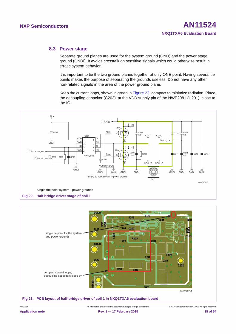
8.3 Power stage
Separate ground planes are used for the system ground (GND) and the power stage ground (GNDI). It avoids crosstalk on sensitive signals which could otherwise result in erratic system behavior.
It is important to tie the two ground planes together at only ONE point. Having several tie points makes the purpose of separating the grounds useless. Do not have any other non-related signals in the area of the power ground plane.
Keep the current loops, shown in green in Figure 22, compact to minimize radiation. Place the decoupling capacitor (C203), at the VDD supply pin of the NWP2081 (U201), close to the IC.
Single the point system - power grounds
Fig 22. Half bridge driver stage of coil 1
aaa-015907
GNDIGNDI
GNDI
+12 V
GNDI GNDIGNDIGND
NODEBRIDGE
Single tie point system to power ground
1VDD
C203
C207
R206
R205 C208n.c.
C211
L1-1
C210
C209n.c. R209
CL1T CL1C
COIL1T COIL1C
G
G
D
S
U201
GND
SD
CLK
GL
[1, 3, 4]IS-
[1, 3, 4]PWM_HIN
[1]EN_HB1
[5]UC1_2SH
GH
FS
2
3
4
8
7
6
5
D
S
NWP2081
T203
T204
GNDI
C214n.c.
C213n.c.
GNDI
C216
GNDI
C217
C205R203T201
Fig 23. PCB layout of half-bridge driver of coil 1 in NXQ1TXA6 evaluation board
aaa-015908
single tie point for the systemand power grounds
compact current loops,decoupling capacitors close by
AN11524 All information provided in this document is subject to legal disclaimers. © NXP Semiconductors N.V. 2015. All rights reserved.
Application note Rev. 1 — 17 February 2015 35 of 54
NXP Semiconductors AN11524NXQ1TXA6 Evaluation Board
8.4 DC-to-DC converter
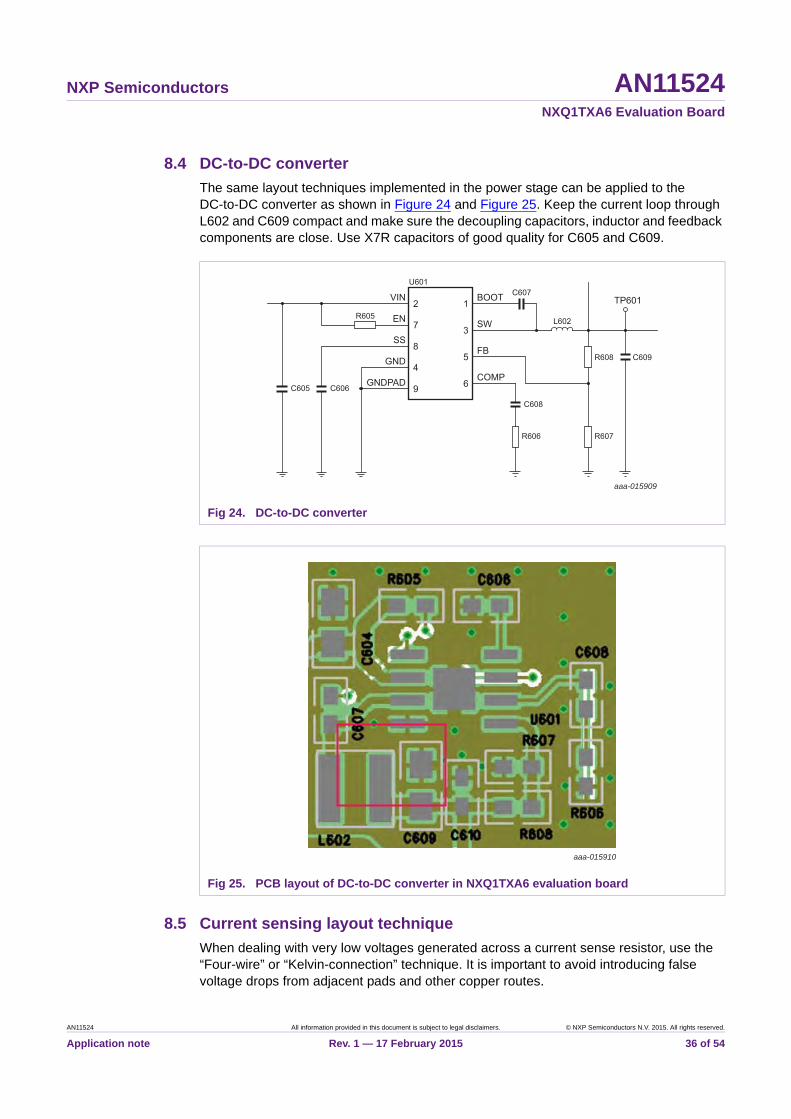
The same layout techniques implemented in the power stage can be applied to the DC-to-DC converter as shown in Figure 24 and Figure 25. Keep the current loop through L602 and C609 compact and make sure the decoupling capacitors, inductor and feedback components are close. Use X7R capacitors of good quality for C605 and C609.
8.5 Current sensing layout technique
When dealing with very low voltages generated across a current sense resistor, use the “Four-wire” or “Kelvin-connection” technique. It is important to avoid introducing false voltage drops from adjacent pads and other copper routes.
Fig 24. DC-to-DC converter
Fig 25. PCB layout of DC-to-DC converter in NXQ1TXA6 evaluation board
aaa-015909
VIN BOOT TP601
SW
FB
COMP
2 1
3
5
6
7
8
4
9
EN
SS
GND
GNDPADC606
R605L602
R607
R608
R606
C605
C608
C609
U601C607
aaa-015910
AN11524 All information provided in this document is subject to legal disclaimers. © NXP Semiconductors N.V. 2015. All rights reserved.
Application note Rev. 1 — 17 February 2015 36 of 54
NXP Semiconductors AN11524NXQ1TXA6 Evaluation Board
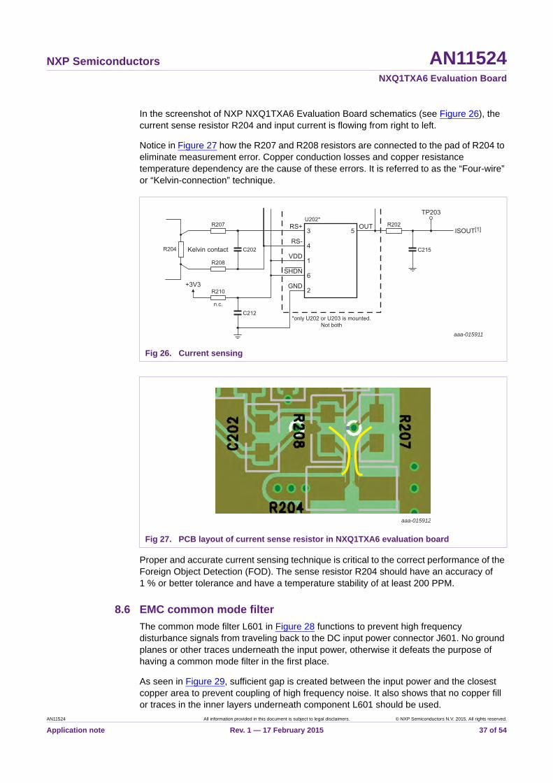
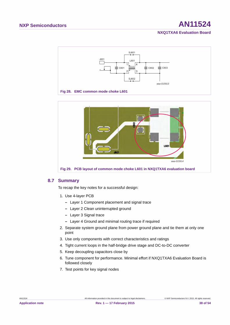
In the screenshot of NXP NXQ1TXA6 Evaluation Board schematics (see Figure 26), the current sense resistor R204 and input current is flowing from right to left.
Notice in Figure 27 how the R207 and R208 resistors are connected to the pad of R204 to eliminate measurement error. Copper conduction losses and copper resistance temperature dependency are the cause of these errors. It is referred to as the “Four-wire” or “Kelvin-connection” technique.
Proper and accurate current sensing technique is critical to the correct performance of the Foreign Object Detection (FOD). The sense resistor R204 should have an accuracy of 1 % or better tolerance and have a temperature stability of at least 200 PPM.
8.6 EMC common mode filter
The common mode filter L601 in Figure 28 functions to prevent high frequency disturbance signals from traveling back to the DC input power connector J601. No ground planes or other traces underneath the input power, otherwise it defeats the purpose of having a common mode filter in the first place.
As seen in Figure 29, sufficient gap is created between the input power and the closest copper area to prevent coupling of high frequency noise. It also shows that no copper fill or traces in the inner layers underneath component L601 should be used.
Fig 26. Current sensing
Fig 27. PCB layout of current sense resistor in NXQ1TXA6 evaluation board
3
4
1
6
OUTISOUT[1]
TP203U202*
*only U202 or U203 is mounted.Not both
C202R204
RS+
RS-
VDD
SHDN
2GND
5
C212
R202
C215
aaa-015911
R207
R210
n.c.
Kelvin contact
+3V3
R208
aaa-015912
AN11524 All information provided in this document is subject to legal disclaimers. © NXP Semiconductors N.V. 2015. All rights reserved.
Application note Rev. 1 — 17 February 2015 37 of 54
NXP Semiconductors AN11524NXQ1TXA6 Evaluation Board
8.7 Summary
To recap the key notes for a successful design:
1. Use 4-layer PCB
– Layer 1 Component placement and signal trace
– Layer 2 Clean uninterrupted ground
– Layer 3 Signal trace
– Layer 4 Ground and minimal routing trace if required
2. Separate system ground plane from power ground plane and tie them at only one point
3. Use only components with correct characteristics and ratings
4. Tight current loops in the half-bridge drive stage and DC-to-DC converter
5. Keep decoupling capacitors close by
6. Tune component for performance. Minimal effort if NXQ1TXA6 Evaluation Board is followed closely
7. Test points for key signal nodes
Fig 28. EMC common mode choke L601
Fig 29. PCB layout of common mode choke L601 in NXQ1TXA6 evaluation board
aaa-015913
J601
C601
SJ601
SJ602
4
3
1
2C602 C603
L601
aaa-015914
AN11524 All information provided in this document is subject to legal disclaimers. © NXP Semiconductors N.V. 2015. All rights reserved.
Application note Rev. 1 — 17 February 2015 38 of 54
NXP Semiconductors AN11524NXQ1TXA6 Evaluation Board
9. Waveforms
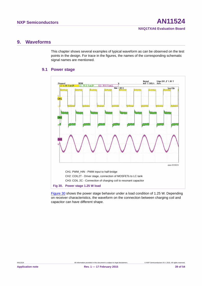
This chapter shows several examples of typical waveform as can be observed on the test points in the design. For trace in the figures, the names of the corresponding schematic signal names are mentioned.
9.1 Power stage
Figure 30 shows the power stage behavior under a load condition of 1.25 W. Depending on receiver characteristics, the waveform on the connection between charging coil and capacitor can have different shape.
CH1: PWM_HIN - PWM input to half-bridge
CH2: COIL2T - Driver stage, connection of MOSFETs to LC tank
CH3: COIL 2C - Connection of charging coil to resonant capacitor
Fig 30. Power stage 1.25 W load
aaa-015915
AN11524 All information provided in this document is subject to legal disclaimers. © NXP Semiconductors N.V. 2015. All rights reserved.
Application note Rev. 1 — 17 February 2015 39 of 54
NXP Semiconductors AN11524NXQ1TXA6 Evaluation Board
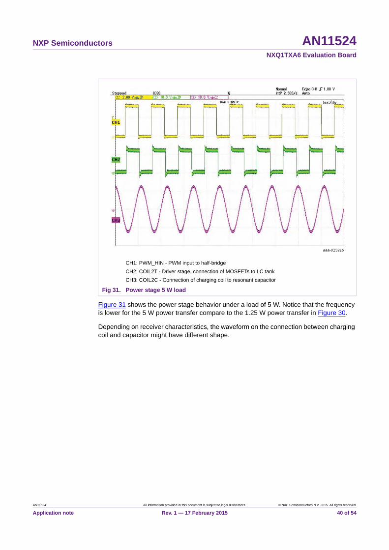
Figure 31 shows the power stage behavior under a load of 5 W. Notice that the frequency is lower for the 5 W power transfer compare to the 1.25 W power transfer in Figure 30.
Depending on receiver characteristics, the waveform on the connection between charging coil and capacitor might have different shape.
CH1: PWM_HIN - PWM input to half-bridge
CH2: COIL2T - Driver stage, connection of MOSFETs to LC tank
CH3: COIL2C - Connection of charging coil to resonant capacitor
Fig 31. Power stage 5 W load
aaa-015916
AN11524 All information provided in this document is subject to legal disclaimers. © NXP Semiconductors N.V. 2015. All rights reserved.
Application note Rev. 1 — 17 February 2015 40 of 54
NXP Semiconductors AN11524NXQ1TXA6 Evaluation Board
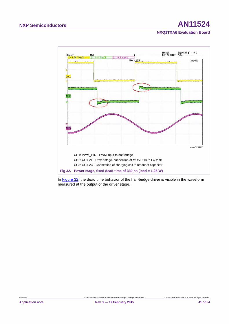
In Figure 32, the dead time behavior of the half-bridge driver is visible in the waveform measured at the output of the driver stage.
CH1: PWM_HIN - PWM input to half-bridge
CH2: COIL2T - Driver stage, connection of MOSFETs to LC tank
CH3: COIL2C - Connection of charging coil to resonant capacitor
Fig 32. Power stage, fixed dead-time of 330 ns (load = 1.25 W)
aaa-015917
AN11524 All information provided in this document is subject to legal disclaimers. © NXP Semiconductors N.V. 2015. All rights reserved.
Application note Rev. 1 — 17 February 2015 41 of 54
NXP Semiconductors AN11524NXQ1TXA6 Evaluation Board
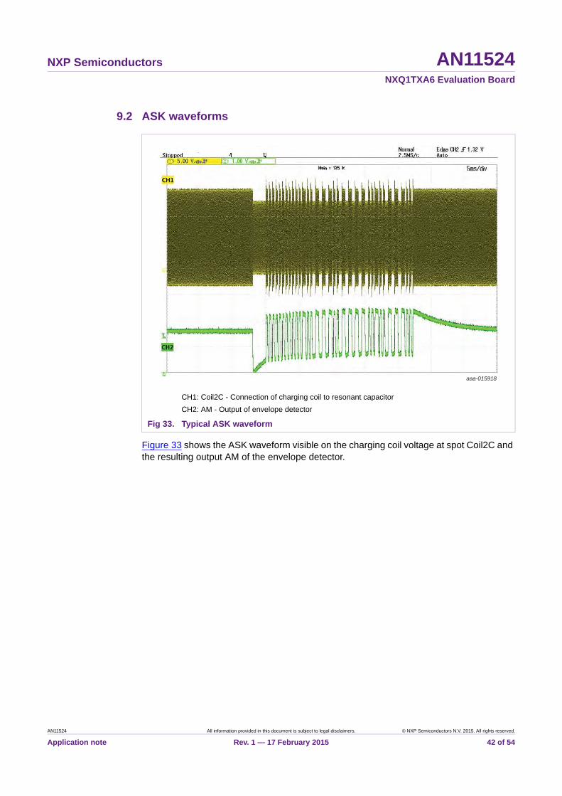
9.2 ASK waveforms
Figure 33 shows the ASK waveform visible on the charging coil voltage at spot Coil2C and the resulting output AM of the envelope detector.
CH1: Coil2C - Connection of charging coil to resonant capacitor
CH2: AM - Output of envelope detector
Fig 33. Typical ASK waveform
aaa-015918
AN11524 All information provided in this document is subject to legal disclaimers. © NXP Semiconductors N.V. 2015. All rights reserved.
Application note Rev. 1 — 17 February 2015 42 of 54
NXP Semiconductors AN11524NXQ1TXA6 Evaluation Board
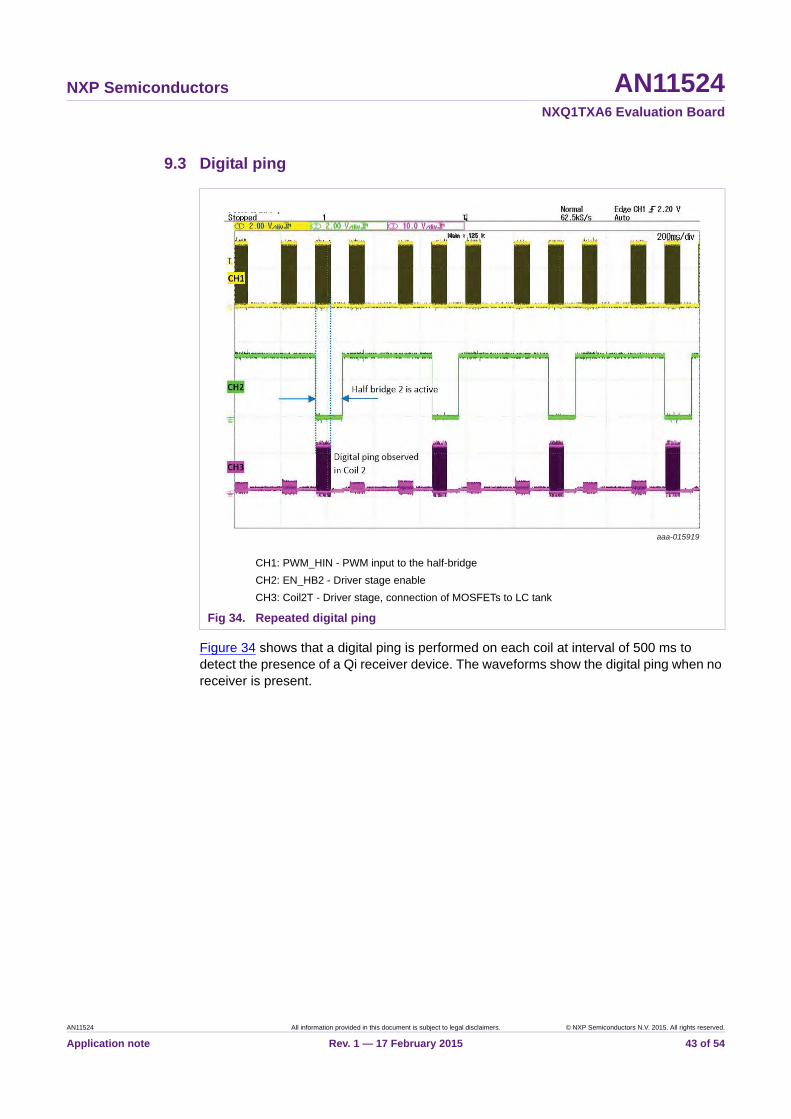
9.3 Digital ping
Figure 34 shows that a digital ping is performed on each coil at interval of 500 ms to detect the presence of a Qi receiver device. The waveforms show the digital ping when no receiver is present.
CH1: PWM_HIN - PWM input to the half-bridge
CH2: EN_HB2 - Driver stage enable
CH3: Coil2T - Driver stage, connection of MOSFETs to LC tank
Fig 34. Repeated digital ping
aaa-015919
AN11524 All information provided in this document is subject to legal disclaimers. © NXP Semiconductors N.V. 2015. All rights reserved.
Application note Rev. 1 — 17 February 2015 43 of 54
NXP Semiconductors AN11524NXQ1TXA6 Evaluation Board
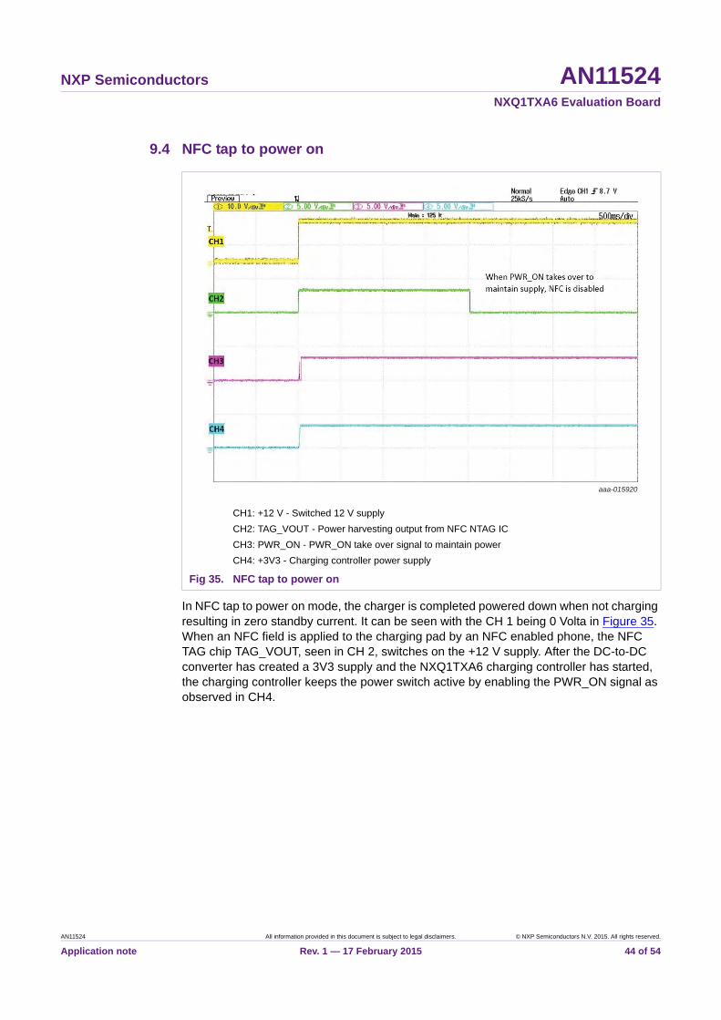
9.4 NFC tap to power on
In NFC tap to power on mode, the charger is completed powered down when not charging resulting in zero standby current. It can be seen with the CH 1 being 0 Volta in Figure 35. When an NFC field is applied to the charging pad by an NFC enabled phone, the NFC TAG chip TAG_VOUT, seen in CH 2, switches on the +12 V supply. After the DC-to-DC converter has created a 3V3 supply and the NXQ1TXA6 charging controller has started, the charging controller keeps the power switch active by enabling the PWR_ON signal as observed in CH4.
CH1: +12 V - Switched 12 V supply
CH2: TAG_VOUT - Power harvesting output from NFC NTAG IC
CH3: PWR_ON - PWR_ON take over signal to maintain power
CH4: +3V3 - Charging controller power supply
Fig 35. NFC tap to power on
aaa-015920
AN11524 All information provided in this document is subject to legal disclaimers. © NXP Semiconductors N.V. 2015. All rights reserved.
Application note Rev. 1 — 17 February 2015 44 of 54
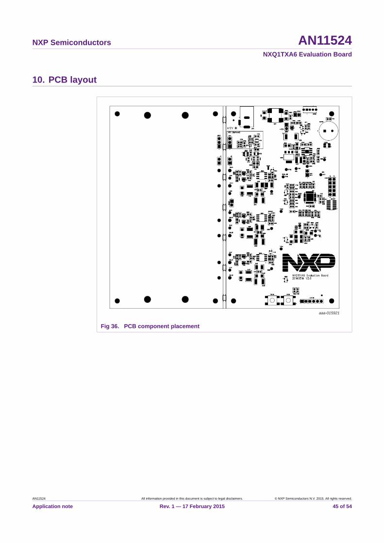
NXP Semiconductors AN11524NXQ1TXA6 Evaluation Board
10. PCB layout
Fig 36. PCB component placement
aaa-015921
AN11524 All information provided in this document is subject to legal disclaimers. © NXP Semiconductors N.V. 2015. All rights reserved.
Application note Rev. 1 — 17 February 2015 45 of 54
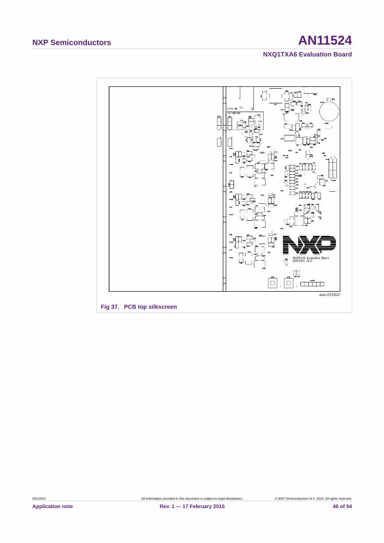
NXP Semiconductors AN11524NXQ1TXA6 Evaluation Board
Fig 37. PCB top silkscreen
aaa-015922
AN11524 All information provided in this document is subject to legal disclaimers. © NXP Semiconductors N.V. 2015. All rights reserved.
Application note Rev. 1 — 17 February 2015 46 of 54
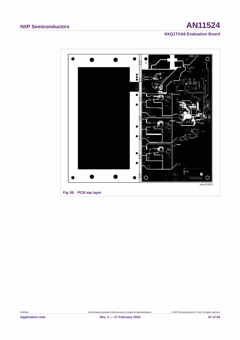
NXP Semiconductors AN11524NXQ1TXA6 Evaluation Board
Fig 38. PCB top layer
aaa-015923
AN11524 All information provided in this document is subject to legal disclaimers. © NXP Semiconductors N.V. 2015. All rights reserved.
Application note Rev. 1 — 17 February 2015 47 of 54
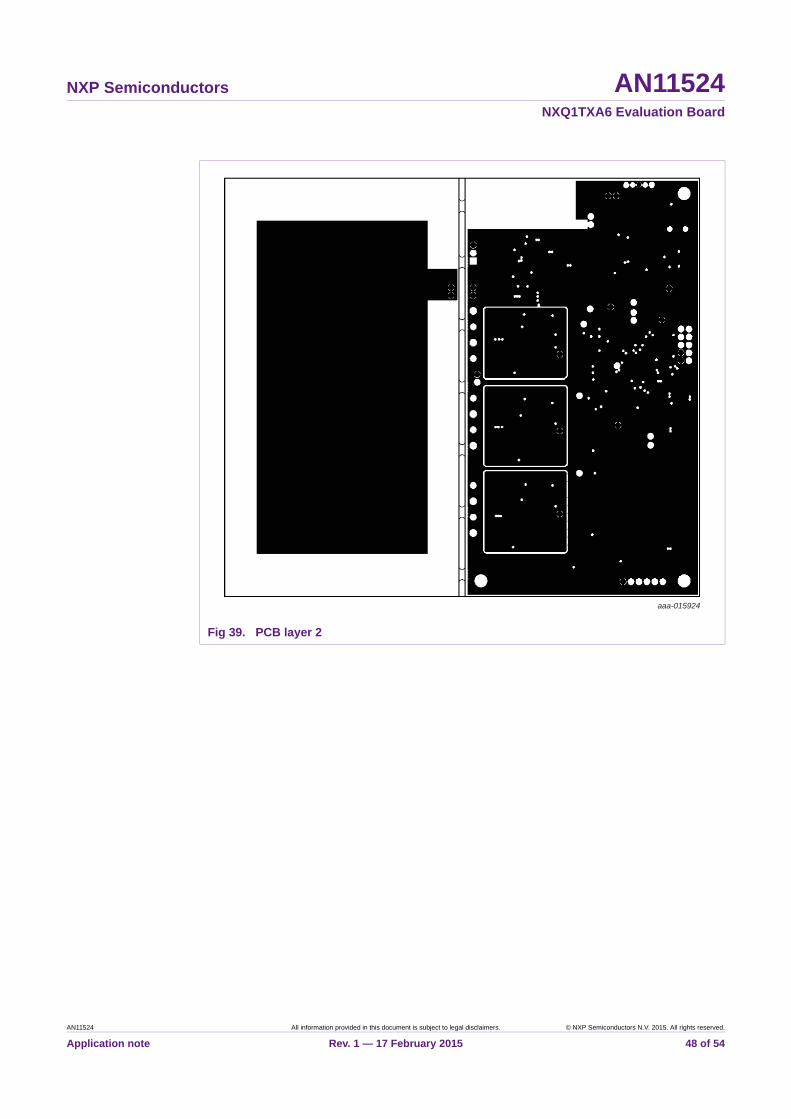
NXP Semiconductors AN11524NXQ1TXA6 Evaluation Board
Fig 39. PCB layer 2
aaa-015924
AN11524 All information provided in this document is subject to legal disclaimers. © NXP Semiconductors N.V. 2015. All rights reserved.
Application note Rev. 1 — 17 February 2015 48 of 54

NXP Semiconductors AN11524NXQ1TXA6 Evaluation Board
Fig 40. PCB layer 3
aaa-015925
AN11524 All information provided in this document is subject to legal disclaimers. © NXP Semiconductors N.V. 2015. All rights reserved.
Application note Rev. 1 — 17 February 2015 49 of 54
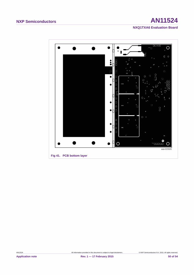
NXP Semiconductors AN11524NXQ1TXA6 Evaluation Board
Fig 41. PCB bottom layer
aaa-015926
AN11524 All information provided in this document is subject to legal disclaimers. © NXP Semiconductors N.V. 2015. All rights reserved.
Application note Rev. 1 — 17 February 2015 50 of 54
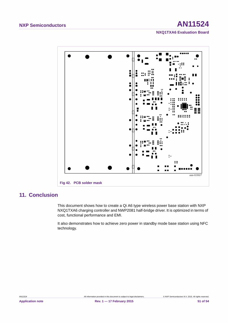
NXP Semiconductors AN11524NXQ1TXA6 Evaluation Board
11. Conclusion
This document shows how to create a Qi A6 type wireless power base station with NXP NXQ1TXA6 charging controller and NWP2081 half-bridge driver. It is optimized in terms of cost, functional performance and EMI.
It also demonstrates how to achieve zero power in standby mode base station using NFC technology.
Fig 42. PCB solder mask
aaa-015927
AN11524 All information provided in this document is subject to legal disclaimers. © NXP Semiconductors N.V. 2015. All rights reserved.
Application note Rev. 1 — 17 February 2015 51 of 54
NXP Semiconductors AN11524NXQ1TXA6 Evaluation Board
12. Legal information
12.1 Definitions
Draft — The document is a draft version only. The content is still under internal review and subject to formal approval, which may result in modifications or additions. NXP Semiconductors does not give any representations or warranties as to the accuracy or completeness of information included herein and shall have no liability for the consequences of use of such information.
12.2 Disclaimers
Limited warranty and liability — Information in this document is believed to be accurate and reliable. However, NXP Semiconductors does not give any representations or warranties, expressed or implied, as to the accuracy or completeness of such information and shall have no liability for the consequences of use of such information. NXP Semiconductors takes no responsibility for the content in this document if provided by an information source outside of NXP Semiconductors.
In no event shall NXP Semiconductors be liable for any indirect, incidental, punitive, special or consequential damages (including - without limitation - lost profits, lost savings, business interruption, costs related to the removal or replacement of any products or rework charges) whether or not such damages are based on tort (including negligence), warranty, breach of contract or any other legal theory.
Notwithstanding any damages that customer might incur for any reason whatsoever, NXP Semiconductors’ aggregate and cumulative liability towards customer for the products described herein shall be limited in accordance with the Terms and conditions of commercial sale of NXP Semiconductors.
Right to make changes — NXP Semiconductors reserves the right to make changes to information published in this document, including without limitation specifications and product descriptions, at any time and without notice. This document supersedes and replaces all information supplied prior to the publication hereof.
Suitability for use — NXP Semiconductors products are not designed, authorized or warranted to be suitable for use in life support, life-critical or safety-critical systems or equipment, nor in applications where failure or malfunction of an NXP Semiconductors product can reasonably be expected to result in personal injury, death or severe property or environmental damage. NXP Semiconductors and its suppliers accept no liability for inclusion and/or use of NXP Semiconductors products in such equipment or applications and therefore such inclusion and/or use is at the customer’s own risk.
Applications — Applications that are described herein for any of these products are for illustrative purposes only. NXP Semiconductors makes no representation or warranty that such applications will be suitable for the specified use without further testing or modification.
Customers are responsible for the design and operation of their applications and products using NXP Semiconductors products, and NXP Semiconductors accepts no liability for any assistance with applications or customer product
design. It is customer’s sole responsibility to determine whether the NXP Semiconductors product is suitable and fit for the customer’s applications and products planned, as well as for the planned application and use of customer’s third party customer(s). Customers should provide appropriate design and operating safeguards to minimize the risks associated with their applications and products.
NXP Semiconductors does not accept any liability related to any default, damage, costs or problem which is based on any weakness or default in the customer’s applications or products, or the application or use by customer’s third party customer(s). Customer is responsible for doing all necessary testing for the customer’s applications and products using NXP Semiconductors products in order to avoid a default of the applications and the products or of the application or use by customer’s third party customer(s). NXP does not accept any liability in this respect.
Export control — This document as well as the item(s) described herein may be subject to export control regulations. Export might require a prior authorization from competent authorities.
Evaluation products — This product is provided on an “as is” and “with all faults” basis for evaluation purposes only. NXP Semiconductors, its affiliates and their suppliers expressly disclaim all warranties, whether express, implied or statutory, including but not limited to the implied warranties of non-infringement, merchantability and fitness for a particular purpose. The entire risk as to the quality, or arising out of the use or performance, of this product remains with customer.
In no event shall NXP Semiconductors, its affiliates or their suppliers be liable to customer for any special, indirect, consequential, punitive or incidental damages (including without limitation damages for loss of business, business interruption, loss of use, loss of data or information, and the like) arising out the use of or inability to use the product, whether or not based on tort (including negligence), strict liability, breach of contract, breach of warranty or any other theory, even if advised of the possibility of such damages.
Notwithstanding any damages that customer might incur for any reason whatsoever (including without limitation, all damages referenced above and all direct or general damages), the entire liability of NXP Semiconductors, its affiliates and their suppliers and customer’s exclusive remedy for all of the foregoing shall be limited to actual damages incurred by customer based on reasonable reliance up to the greater of the amount actually paid by customer for the product or five dollars (US$5.00). The foregoing limitations, exclusions and disclaimers shall apply to the maximum extent permitted by applicable law, even if any remedy fails of its essential purpose.
Translations — A non-English (translated) version of a document is for reference only. The English version shall prevail in case of any discrepancy between the translated and English versions.
12.3 TrademarksNotice: All referenced brands, product names, service names and trademarks are the property of their respective owners.
I2C-bus — logo is a trademark of NXP Semiconductors N.V.
AN11524 All information provided in this document is subject to legal disclaimers. © NXP Semiconductors N.V. 2015. All rights reserved.
Application note Rev. 1 — 17 February 2015 52 of 54
NXP Semiconductors AN11524NXQ1TXA6 Evaluation Board
13. Tables
Table 1. LED status indicator . . . . . . . . . . . . . . . . . . . . . .9Table 2. NXP components for wireless charger
application . . . . . . . . . . . . . . . . . . . . . . . . . . . . 10Table 3. Bill Of Materials (BOM) . . . . . . . . . . . . . . . . . . 22
14. Figures
Fig 1. Wireless charging system as defined by Wireless Power Consortium . . . . . . . . . . . . . . . . . . . . . . . . .3
Fig 2. Overview of the charging pad . . . . . . . . . . . . . . . .5Fig 3. System efficiency . . . . . . . . . . . . . . . . . . . . . . . . . .6Fig 4. Switch, buttons and status LED location overview 7Fig 5. Standby-by power mode switch . . . . . . . . . . . . . . .8Fig 6. NXQ1TXA6 evaluation board block diagram . . . .12Fig 7. NXQ1TXA6 charging controller schematic . . . . .16Fig 8. Half bridge driver stage of coil 1 and current
sense schematic . . . . . . . . . . . . . . . . . . . . . . . . .17Fig 9. Half bridge driver stage of coil 2 and 3 . . . . . . . .18Fig 10. Amplitude Shift Keying (ASK) envelope detector
schematic. . . . . . . . . . . . . . . . . . . . . . . . . . . . . . .19Fig 11. DC supply schematic . . . . . . . . . . . . . . . . . . . . . .20Fig 12. NFC schematic . . . . . . . . . . . . . . . . . . . . . . . . . .21Fig 13. LC tank circuit of coil 1. . . . . . . . . . . . . . . . . . . . .28Fig 14. Half bridge driver, MOSFET and capacitor
snubber circuits of coil 1 . . . . . . . . . . . . . . . . . . .29Fig 15. Current sense resistor . . . . . . . . . . . . . . . . . . . . .30Fig 16. Amplitude Shift Keying (ASK) envelope detector.30Fig 17. Configuration and voltage measurement . . . . . . .31Fig 18. Temperature sensing circuit . . . . . . . . . . . . . . . . .32Fig 19. Tuning capacitor NFC antenna . . . . . . . . . . . . . .32Fig 20. NXQ1TXA6 charging controller supply
decoupling capacitors . . . . . . . . . . . . . . . . . . . . .34Fig 21. Decoupling capacitors (left) & GND stitching
vias underneath NXQ1TXA6 (right) . . . . . . . . . . .34Fig 22. Half bridge driver stage of coil 1 . . . . . . . . . . . . .35Fig 23. PCB layout of half-bridge driver of coil 1 in
NXQ1TXA6 evaluation board . . . . . . . . . . . . . . .35Fig 24. DC-to-DC converter . . . . . . . . . . . . . . . . . . . . . . .36Fig 25. PCB layout of DC-to-DC converter in
NXQ1TXA6 evaluation board . . . . . . . . . . . . . . .36Fig 26. Current sensing . . . . . . . . . . . . . . . . . . . . . . . . . .37Fig 27. PCB layout of current sense resistor in
NXQ1TXA6 evaluation board . . . . . . . . . . . . . . .37Fig 28. EMC common mode choke L601. . . . . . . . . . . . .38Fig 29. PCB layout of common mode choke L601 in
NXQ1TXA6 evaluation board . . . . . . . . . . . . . . .38Fig 30. Power stage 1.25 W load. . . . . . . . . . . . . . . . . . .39Fig 31. Power stage 5 W load . . . . . . . . . . . . . . . . . . . . .40Fig 32. Power stage, fixed dead-time of 330 ns
(load = 1.25 W) . . . . . . . . . . . . . . . . . . . . . . . . . .41Fig 33. Typical ASK waveform. . . . . . . . . . . . . . . . . . . . .42Fig 34. Repeated digital ping . . . . . . . . . . . . . . . . . . . . . .43Fig 35. NFC tap to power on . . . . . . . . . . . . . . . . . . . . . .44Fig 36. PCB component placement . . . . . . . . . . . . . . . . .45Fig 37. PCB top silkscreen . . . . . . . . . . . . . . . . . . . . . . .46Fig 38. PCB top layer. . . . . . . . . . . . . . . . . . . . . . . . . . . .47Fig 39. PCB layer 2 . . . . . . . . . . . . . . . . . . . . . . . . . . . . .48
Fig 40. PCB layer 3 . . . . . . . . . . . . . . . . . . . . . . . . . . . . . 49Fig 41. PCB bottom layer . . . . . . . . . . . . . . . . . . . . . . . . 50Fig 42. PCB solder mask . . . . . . . . . . . . . . . . . . . . . . . . 51
AN11524 All information provided in this document is subject to legal disclaimers. © NXP Semiconductors N.V. 2015. All rights reserved.
Application note Rev. 1 — 17 February 2015 53 of 54
NXP Semiconductors AN11524NXQ1TXA6 Evaluation Board
15. Contents
1 Introduction . . . . . . . . . . . . . . . . . . . . . . . . . . . . 3
2 Scope . . . . . . . . . . . . . . . . . . . . . . . . . . . . . . . . . 4
3 Getting started . . . . . . . . . . . . . . . . . . . . . . . . . . 53.1 Package contents . . . . . . . . . . . . . . . . . . . . . . . 53.2 Main features . . . . . . . . . . . . . . . . . . . . . . . . . . 63.3 System efficiency . . . . . . . . . . . . . . . . . . . . . . . 63.4 Board overview. . . . . . . . . . . . . . . . . . . . . . . . . 63.5 Stand-by power mode switch . . . . . . . . . . . . . . 83.6 Reset button . . . . . . . . . . . . . . . . . . . . . . . . . . . 83.7 Foreign object detection button . . . . . . . . . . . . 83.8 Status LED . . . . . . . . . . . . . . . . . . . . . . . . . . . . 93.9 NFC functionality . . . . . . . . . . . . . . . . . . . . . . . 9
4 NXP product offering. . . . . . . . . . . . . . . . . . . . 10
5 System overview . . . . . . . . . . . . . . . . . . . . . . . 115.1 NXQ1TXA6 charging controller . . . . . . . . . . . 135.2 Half Bridge driver . . . . . . . . . . . . . . . . . . . . . . 135.3 Amplitude-Shift Keying (ASK) envelope
demodulator . . . . . . . . . . . . . . . . . . . . . . . . . . 135.4 +12 V universal mains adapter . . . . . . . . . . . . 135.5 Current measurement. . . . . . . . . . . . . . . . . . . 145.6 Bandgap reference voltage. . . . . . . . . . . . . . . 145.7 DC-to-DC converter . . . . . . . . . . . . . . . . . . . . 145.8 Near Field Communication (NFC) zero
power in Standby mode . . . . . . . . . . . . . . . . . 14
6 Schematics and Bill Of Materials . . . . . . . . . . 156.1 Schematics . . . . . . . . . . . . . . . . . . . . . . . . . . . 166.2 Bill Of Materials . . . . . . . . . . . . . . . . . . . . . . . 21
7 Critical components . . . . . . . . . . . . . . . . . . . . 287.1 Power stage . . . . . . . . . . . . . . . . . . . . . . . . . . 287.1.1 Capacitor in LC tank circuit. . . . . . . . . . . . . . . 287.1.2 Half-bridge driver and MOSFETs . . . . . . . . . . 287.1.3 Capacitor snubber circuits . . . . . . . . . . . . . . . 297.2 Current sense resistor . . . . . . . . . . . . . . . . . . 297.3 Amplitude-Shift Keying envelope detector . . . 307.4 Configuration and voltage measurement
circuits. . . . . . . . . . . . . . . . . . . . . . . . . . . . . . . 307.5 Thermal protection . . . . . . . . . . . . . . . . . . . . . 317.6 NFC antenna tuning capacitor . . . . . . . . . . . . 32
8 PCB layout guidelines. . . . . . . . . . . . . . . . . . . 338.1 Ground planes . . . . . . . . . . . . . . . . . . . . . . . . 338.2 NXQ1TXA6 charging controller . . . . . . . . . . . 338.3 Power stage . . . . . . . . . . . . . . . . . . . . . . . . . . 358.4 DC-to-DC converter . . . . . . . . . . . . . . . . . . . . 368.5 Current sensing layout technique . . . . . . . . . . 368.6 EMC common mode filter . . . . . . . . . . . . . . . . 378.7 Summary . . . . . . . . . . . . . . . . . . . . . . . . . . . . 38
9 Waveforms. . . . . . . . . . . . . . . . . . . . . . . . . . . . 399.1 Power stage . . . . . . . . . . . . . . . . . . . . . . . . . . 399.2 ASK waveforms . . . . . . . . . . . . . . . . . . . . . . . 429.3 Digital ping . . . . . . . . . . . . . . . . . . . . . . . . . . . 439.4 NFC tap to power on . . . . . . . . . . . . . . . . . . . 44
10 PCB layout . . . . . . . . . . . . . . . . . . . . . . . . . . . . 45
11 Conclusion. . . . . . . . . . . . . . . . . . . . . . . . . . . . 51
12 Legal information . . . . . . . . . . . . . . . . . . . . . . 5212.1 Definitions . . . . . . . . . . . . . . . . . . . . . . . . . . . 5212.2 Disclaimers . . . . . . . . . . . . . . . . . . . . . . . . . . 5212.3 Trademarks . . . . . . . . . . . . . . . . . . . . . . . . . . 52
13 Tables . . . . . . . . . . . . . . . . . . . . . . . . . . . . . . . . 53
14 Figures . . . . . . . . . . . . . . . . . . . . . . . . . . . . . . . 53
15 Contents. . . . . . . . . . . . . . . . . . . . . . . . . . . . . . 54
© NXP Semiconductors N.V. 2015. All rights reserved.
For more information, please visit: http://www.nxp.comFor sales office addresses, please send an email to: [email protected]
Date of release: 17 February 2015
Document identifier: AN11524
Please be aware that important notices concerning this document and the product(s)described herein, have been included in section ‘Legal information’.
Recommended