RT5760
Copyright © 2019 Richtek Technology Corporation. All rights reserved. is a registered trademark of Richtek Technology Corporation.
DS5760-02 December 2019 www.richtek.com 1
6V Input, 1A, ACOTTM Buck Converter in Thin SOT-563 Package
General Description
The RT5760 is a simple, easy-to-use, 1A synchronous
step-down DC-DC converter with an input supply
voltage range of 2.5V to 6V. The device build-in an
accurate 0.6V reference voltage and integrates low
RDS(ON) power MOSFETs to achieve high efficiency in
a SOT-563 (FC) package.
The RT5760 adopts Advanced Constant On-Time
(ACOTTM) control architecture to provide an ultrafast
transient response with few external components and
to operate in nearly constant switching frequency over
the line, load, and output voltage range. The RT5760A
operates in automatic PSM that maintains high
efficiency during light load operation. The RT5760B
operates in Forced PWM that helps meet tight voltage
regulation accuracy requirements. The RT5760C/D
remove the power good indicator function of the
RT5760A/B for different application.
The RT5760 senses both FETs current for a robust
over-current protection. The device features
cycle-by-cycle current limit protection and prevent the
device from the catastrophic damage in output short
circuit, over current or inductor saturation. A built-in
soft-start function prevents inrush current during
start-up. The device also includes input under-voltage
lockout, output under-voltage protection, and
over-temperature protection (thermal shutdown) to
provide safe and smooth operation in all operating
conditions.
Features Input Voltage Range of 2.5V to 6V
Integrated 120m and 80m FETs
1A Output Current, up to 95% Efficiency
100% Duty Cycle for Lowest Dropout
0.6V, 1% Internal Reference Voltage
2.2MHz Typical Switching Frequency
Power Saving Mode for Light Loads (RT5760A/C)
Low Shutdown Current 1A
Low Quiescent Current: 25A (Typ.)
Fast Advanced Constant On-Time (ACOTTM)
Control
Internal Soft Startup (0.6ms)
Independent Enable Control Input
Power Good Indicator
Both FETs Over-Current Protection
Input Under-Voltage Lockout Protection
Hiccup-Mode Output Under-Voltage Protection
Over-Temperature Protection (Thermal Shutdown)
RoHS Compliant and Halogen Free
Applications Mobile Phones and Handheld Devices
STB, Cable Modem, and xDSL Platforms
WLAN ASIC Power / Storage (SSD and HDD)
General Purpose for POL LV Buck Converter
Simplified Application Circuit
EN
RT5760
FBGND
VINVINCIN
**PG
L
COUT
SW VOUT
RFB1Enable
RFB2
*CFF
VPG
RPG
*CFF : Optional for performance fine-tune
**PG : RT5760A/B only.

RT5760
Copyright © 2019 Richtek Technology Corporation. All rights reserved. is a registered trademark of Richtek Technology Corporation.
www.richtek.com DS5760-02 December 2019 2
Ordering Information
RT5760
Package Type
H6F : SOT-563 (FC)
Lead Plating System
G : Green (Halogen Free and Pb Free)
UVP Option
H : Hiccup
PWM Operation Mode
A : Automatic PSM
B : Forced PWM
C : Automatic PSM
D : Forced PWM
Note :
Richtek products are :
RoHS compliant and compatible with the current
requirements of IPC/JEDEC J-STD-020.
Suitable for use in SnPb or Pb-free soldering processes.
Marking Information
RT5760AHGH6F03 : Product Code
W : Date Code03W
RT5760BHGH6F02 : Product Code
W : Date Code02W
0A : Product Code
W : Date Code
RT5760DHGH6F
0AW
RT5760CHGH6F0B : Product Code
W : Date Code0BW
Pin Configuration
(TOP VIEW)
FB GND VIN
PG EN SW
4
2 3
56
1
SOT-563 (FC) (RT5760A/B)
FB GND VIN
NC EN SW
4
2 3
56
1
SOT-563 (FC) (RT5760C/D)

RT5760
Copyright © 2019 Richtek Technology Corporation. All rights reserved. is a registered trademark of Richtek Technology Corporation.
DS5760-02 December 2019 www.richtek.com 3
Functional Pin Description
Pin No. Pin Name Pin Function
RT5760A/B RT5760C/D
1 1 FB
Feedback voltage input. Connect this pin to the midpoint of the external
feedback resistive divider to set the output voltage of the converter to
the desired regulation level. The device regulates the FB voltage at
Feedback Reference Voltage, typically 0.6V.
2 2 GND Signal and power ground pin. Place the bottom resistor of the feedback
network as close as possible to this pin.
3 3 VIN
Power input. The input voltage range is from 2.5V to 6V. Connect input
bypass capacitors directly to this pin and GND pins. MLCC with
capacitance higher than 10F is recommended.
4 4 SW Switch node between the internal switch and the synchronous rectifier.
Connect this pin to the inductor.
5 5 EN
Enable control input. Connect this pin to logic high can enable the
device and connect this pin to GND can disable the device. Do not
leave floating.
6 -- PG
Power good indicator. The output of this pin is an open-drain with
external pull-up resistor. After soft startup, PG is pulled up when the FB
voltage is within 90% (typ.).
-- 6 NC No internal connection.
RT5760
Copyright © 2019 Richtek Technology Corporation. All rights reserved. is a registered trademark of Richtek Technology Corporation.
www.richtek.com DS5760-02 December 2019 4
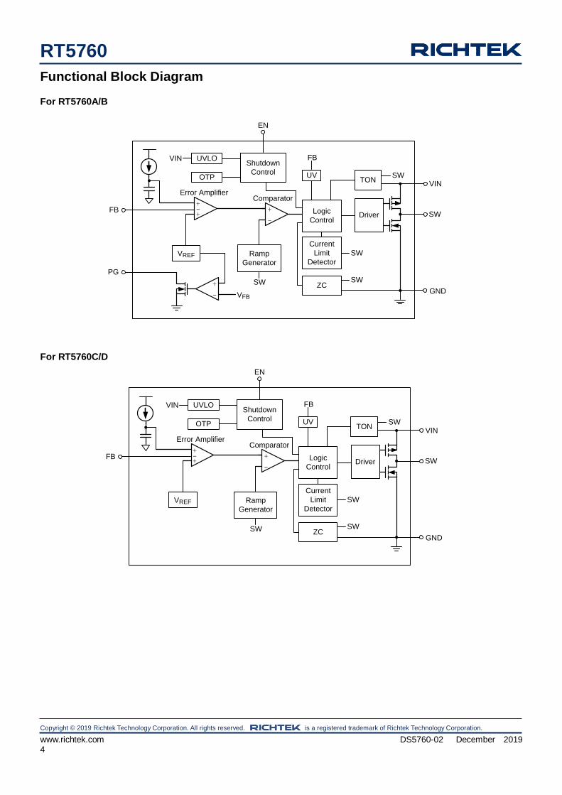
Functional Block Diagram
For RT5760A/B
VIN
GND
EN
+
-
VREF
Shutdown
Control
SWFB
Driver
TON
Logic
Control
SW
Current
Limit
Detector
ZCSW
Comparator+-+
Error Amplifier
UVLO
OTP
SW
+
-
VFB
PG
Ramp
Generator
SW
UV
FBVIN
For RT5760C/D
VIN
GND
EN
+
-
VREF
Shutdown
Control
SWFB
Driver
TON
Logic
Control
SW
Current
Limit
Detector
ZCSW
Comparator+-+
Error Amplifier
UVLO
OTP
SWRamp
Generator
SW
UV
FBVIN
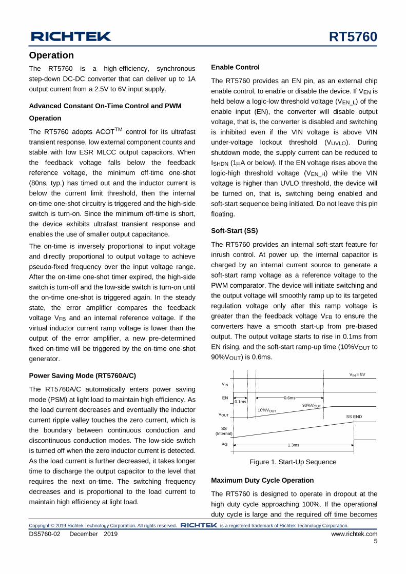
RT5760
Copyright © 2019 Richtek Technology Corporation. All rights reserved. is a registered trademark of Richtek Technology Corporation.
DS5760-02 December 2019 www.richtek.com 5
Operation
The RT5760 is a high-efficiency, synchronous
step-down DC-DC converter that can deliver up to 1A
output current from a 2.5V to 6V input supply.
Advanced Constant On-Time Control and PWM
Operation
The RT5760 adopts ACOTTM control for its ultrafast
transient response, low external component counts and
stable with low ESR MLCC output capacitors. When
the feedback voltage falls below the feedback
reference voltage, the minimum off-time one-shot
(80ns, typ.) has timed out and the inductor current is
below the current limit threshold, then the internal
on-time one-shot circuitry is triggered and the high-side
switch is turn-on. Since the minimum off-time is short,
the device exhibits ultrafast transient response and
enables the use of smaller output capacitance.
The on-time is inversely proportional to input voltage
and directly proportional to output voltage to achieve
pseudo-fixed frequency over the input voltage range.
After the on-time one-shot timer expired, the high-side
switch is turn-off and the low-side switch is turn-on until
the on-time one-shot is triggered again. In the steady
state, the error amplifier compares the feedback
voltage VFB and an internal reference voltage. If the
virtual inductor current ramp voltage is lower than the
output of the error amplifier, a new pre-determined
fixed on-time will be triggered by the on-time one-shot
generator.
Power Saving Mode (RT5760A/C)
The RT5760A/C automatically enters power saving
mode (PSM) at light load to maintain high efficiency. As
the load current decreases and eventually the inductor
current ripple valley touches the zero current, which is
the boundary between continuous conduction and
discontinuous conduction modes. The low-side switch
is turned off when the zero inductor current is detected.
As the load current is further decreased, it takes longer
time to discharge the output capacitor to the level that
requires the next on-time. The switching frequency
decreases and is proportional to the load current to
maintain high efficiency at light load.
Enable Control
The RT5760 provides an EN pin, as an external chip
enable control, to enable or disable the device. If VEN is
held below a logic-low threshold voltage (VEN_L) of the
enable input (EN), the converter will disable output
voltage, that is, the converter is disabled and switching
is inhibited even if the VIN voltage is above VIN
under-voltage lockout threshold (VUVLO). During
shutdown mode, the supply current can be reduced to
ISHDN (1A or below). If the EN voltage rises above the
logic-high threshold voltage (VEN_H) while the VIN
voltage is higher than UVLO threshold, the device will
be turned on, that is, switching being enabled and
soft-start sequence being initiated. Do not leave this pin
floating.
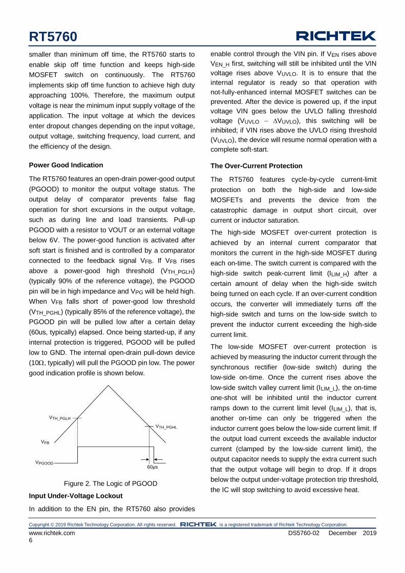
Soft-Start (SS)
The RT5760 provides an internal soft-start feature for
inrush control. At power up, the internal capacitor is
charged by an internal current source to generate a
soft-start ramp voltage as a reference voltage to the
PWM comparator. The device will initiate switching and
the output voltage will smoothly ramp up to its targeted
regulation voltage only after this ramp voltage is
greater than the feedback voltage VFB to ensure the
converters have a smooth start-up from pre-biased
output. The output voltage starts to rise in 0.1ms from
EN rising, and the soft-start ramp-up time (10%VOUT to
90%VOUT) is 0.6ms.
VOUT
EN
VIN
0.6ms
VIN = 5V
10%VOUT
90%VOUT
0.1ms
PG 1.3ms
SS
(Internal)
SS END
Figure 1. Start-Up Sequence
Maximum Duty Cycle Operation
The RT5760 is designed to operate in dropout at the
high duty cycle approaching 100%. If the operational
duty cycle is large and the required off time becomes
RT5760
Copyright © 2019 Richtek Technology Corporation. All rights reserved. is a registered trademark of Richtek Technology Corporation.
www.richtek.com DS5760-02 December 2019 6
smaller than minimum off time, the RT5760 starts to
enable skip off time function and keeps high-side
MOSFET switch on continuously. The RT5760
implements skip off time function to achieve high duty
approaching 100%. Therefore, the maximum output
voltage is near the minimum input supply voltage of the
application. The input voltage at which the devices
enter dropout changes depending on the input voltage,
output voltage, switching frequency, load current, and
the efficiency of the design.
Power Good Indication
The RT5760 features an open-drain power-good output
(PGOOD) to monitor the output voltage status. The
output delay of comparator prevents false flag
operation for short excursions in the output voltage,
such as during line and load transients. Pull-up
PGOOD with a resistor to VOUT or an external voltage
below 6V. The power-good function is activated after
soft start is finished and is controlled by a comparator
connected to the feedback signal VFB. If VFB rises
above a power-good high threshold (VTH_PGLH)
(typically 90% of the reference voltage), the PGOOD
pin will be in high impedance and VPG will be held high.
When VFB falls short of power-good low threshold
(VTH_PGHL) (typically 85% of the reference voltage), the
PGOOD pin will be pulled low after a certain delay
(60us, typically) elapsed. Once being started-up, if any
internal protection is triggered, PGOOD will be pulled
low to GND. The internal open-drain pull-down device
(10, typically) will pull the PGOOD pin low. The power
good indication profile is shown below.
VTH_PGLH
VTH_PGHL
VFB
VPGOOD60μs
Figure 2. The Logic of PGOOD
Input Under-Voltage Lockout
In addition to the EN pin, the RT5760 also provides
enable control through the VIN pin. If VEN rises above
VEN_H first, switching will still be inhibited until the VIN
voltage rises above VUVLO. It is to ensure that the
internal regulator is ready so that operation with
not-fully-enhanced internal MOSFET switches can be
prevented. After the device is powered up, if the input
voltage VIN goes below the UVLO falling threshold
voltage (VUVLO VUVLO), this switching will be
inhibited; if VIN rises above the UVLO rising threshold
(VUVLO), the device will resume normal operation with a
complete soft-start.
The Over-Current Protection
The RT5760 features cycle-by-cycle current-limit
protection on both the high-side and low-side
MOSFETs and prevents the device from the
catastrophic damage in output short circuit, over
current or inductor saturation.
The high-side MOSFET over-current protection is
achieved by an internal current comparator that
monitors the current in the high-side MOSFET during
each on-time. The switch current is compared with the
high-side switch peak-current limit (ILIM_H) after a
certain amount of delay when the high-side switch
being turned on each cycle. If an over-current condition
occurs, the converter will immediately turns off the
high-side switch and turns on the low-side switch to
prevent the inductor current exceeding the high-side
current limit.
The low-side MOSFET over-current protection is
achieved by measuring the inductor current through the
synchronous rectifier (low-side switch) during the
low-side on-time. Once the current rises above the
low-side switch valley current limit (ILIM_L), the on-time
one-shot will be inhibited until the inductor current
ramps down to the current limit level (ILIM_L), that is,
another on-time can only be triggered when the
inductor current goes below the low-side current limit. If
the output load current exceeds the available inductor
current (clamped by the low-side current limit), the
output capacitor needs to supply the extra current such
that the output voltage will begin to drop. If it drops
below the output under-voltage protection trip threshold,
the IC will stop switching to avoid excessive heat.
RT5760
Copyright © 2019 Richtek Technology Corporation. All rights reserved. is a registered trademark of Richtek Technology Corporation.
DS5760-02 December 2019 www.richtek.com 7
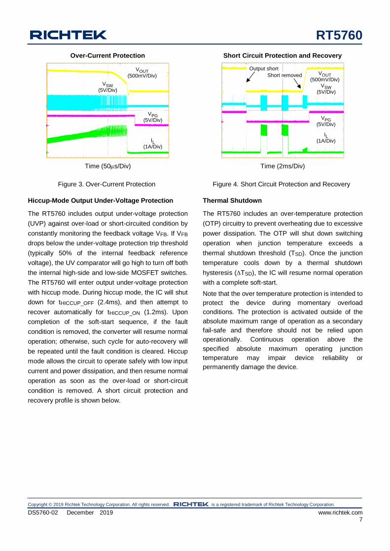
Figure 3. Over-Current Protection
Hiccup-Mode Output Under-Voltage Protection
The RT5760 includes output under-voltage protection
(UVP) against over-load or short-circuited condition by
constantly monitoring the feedback voltage VFB. If VFB
drops below the under-voltage protection trip threshold
(typically 50% of the internal feedback reference
voltage), the UV comparator will go high to turn off both
the internal high-side and low-side MOSFET switches.
The RT5760 will enter output under-voltage protection
with hiccup mode. During hiccup mode, the IC will shut
down for tHICCUP_OFF (2.4ms), and then attempt to
recover automatically for tHICCUP_ON (1.2ms). Upon
completion of the soft-start sequence, if the fault
condition is removed, the converter will resume normal
operation; otherwise, such cycle for auto-recovery will
be repeated until the fault condition is cleared. Hiccup
mode allows the circuit to operate safely with low input
current and power dissipation, and then resume normal
operation as soon as the over-load or short-circuit
condition is removed. A short circuit protection and
recovery profile is shown below.
Figure 4. Short Circuit Protection and Recovery
Thermal Shutdown
The RT5760 includes an over-temperature protection
(OTP) circuitry to prevent overheating due to excessive
power dissipation. The OTP will shut down switching
operation when junction temperature exceeds a
thermal shutdown threshold (TSD). Once the junction
temperature cools down by a thermal shutdown
hysteresis (TSD), the IC will resume normal operation
with a complete soft-start.
Note that the over temperature protection is intended to
protect the device during momentary overload
conditions. The protection is activated outside of the
absolute maximum range of operation as a secondary
fail-safe and therefore should not be relied upon
operationally. Continuous operation above the
specified absolute maximum operating junction
temperature may impair device reliability or
permanently damage the device.
Time (50s/Div)
Over-Current Protection
VOUT(500mV/Div)
VSW(5V/Div)
VPG(5V/Div)
IL(1A/Div)
Time (2ms/Div)
Output shortVOUT
(500mV/Div)VSW
(5V/Div)
VPG(5V/Div)
IL(1A/Div)
Short Circuit Protection and Recovery
Short removed

RT5760
Copyright © 2019 Richtek Technology Corporation. All rights reserved. is a registered trademark of Richtek Technology Corporation.
www.richtek.com DS5760-02 December 2019 8
Absolute Maximum Ratings (Note 1)
Supply Input Voltage, VIN --------------------------------------------------------------------------------------- 0.3V to 6.5V
Switch Voltage, SW ----------------------------------------------------------------------------------------------- 0.3V to 6.5V
< 50ns ---------------------------------------------------------------------------------------------------------------- 2.5V to 9V
Other Pins ----------------------------------------------------------------------------------------------------------- 0.3V to 6.5V
Power Dissipation, PD @ TA = 25C
SOT-563 (FC) ------------------------------------------------------------------------------------------------------ 1W
Lead Temperature (Soldering, 10 sec.) ---------------------------------------------------------------------- 260C
Junction Temperature -------------------------------------------------------------------------------------------- 150C
Storage Temperature Range ----------------------------------------------------------------------------------- 65C to 150C
ESD Ratings
ESD Susceptibility (Note 2)
HBM (Human Body Model) ------------------------------------------------------------------------------------- 2kV
Recommended Operating Conditions (Note 3)
Supply Input Voltage --------------------------------------------------------------------------------------------- 2.5V to 6V
Output Voltage ----------------------------------------------------------------------------------------------------- 0.6V to VIN
Junction Temperature Range ---------------------------------------------------------------------------------- 40C to 125C
Thermal Information (Note 4 and Note 5)
Thermal Parameter SOT-563 (FC) Unit
JA Junction-to-ambient thermal resistance (JEDEC
standard) 109.4 C/W
JC(Top) Junction-to-case (top) thermal resistance 7.3 C/W
JC(Bottom) Junction-to-case (bottom) thermal resistance 18.1 C/W
JA(EVB) Junction-to-ambient thermal resistance (specific EVB) 100 C/W
JC(Top) Junction-to-top characterization parameter 13 C/W
RT5760
Copyright © 2019 Richtek Technology Corporation. All rights reserved. is a registered trademark of Richtek Technology Corporation.
DS5760-02 December 2019 www.richtek.com 9
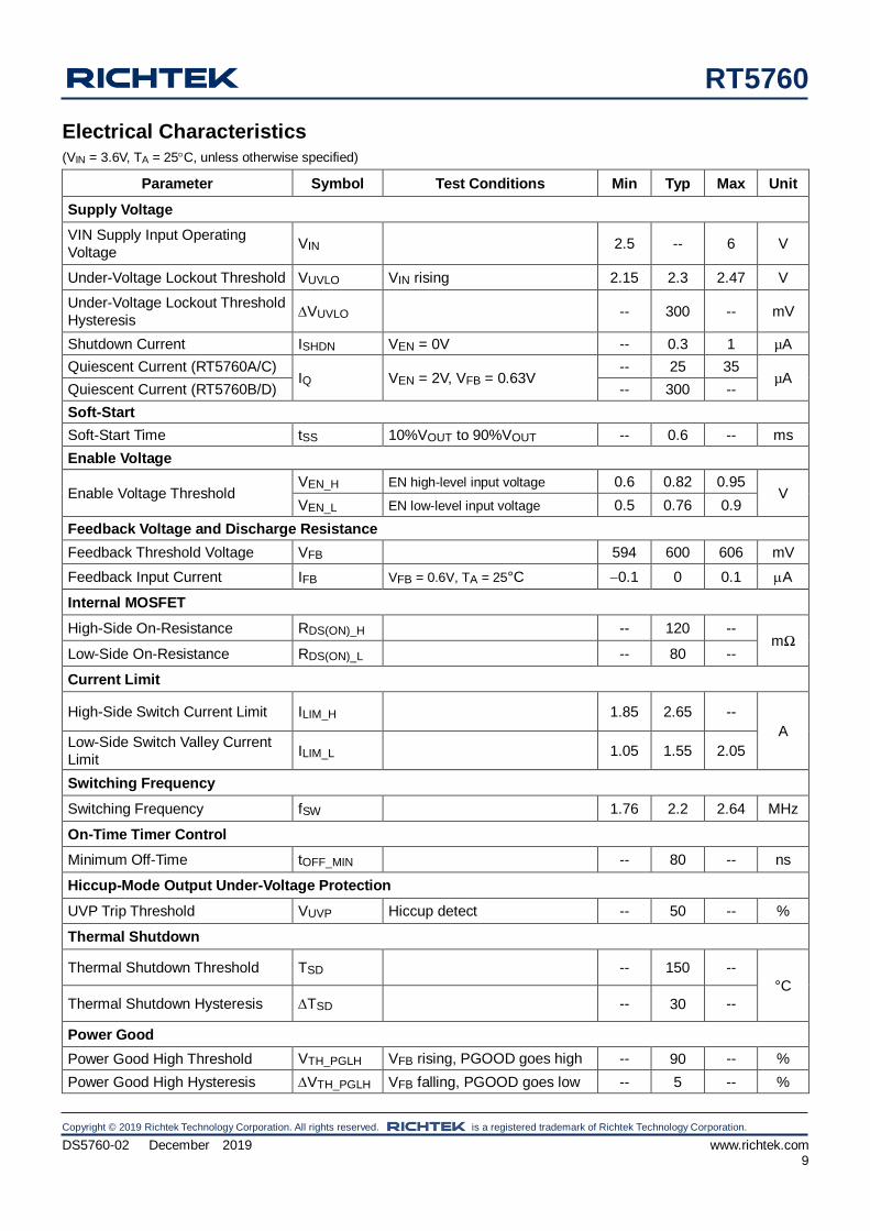
Electrical Characteristics (VIN = 3.6V, TA = 25C, unless otherwise specified)
Parameter Symbol Test Conditions Min Typ Max Unit
Supply Voltage
VIN Supply Input Operating
Voltage VIN 2.5 -- 6 V
Under-Voltage Lockout Threshold VUVLO VIN rising 2.15 2.3 2.47 V
Under-Voltage Lockout Threshold
Hysteresis VUVLO -- 300 -- mV
Shutdown Current ISHDN VEN = 0V -- 0.3 1 µA
Quiescent Current (RT5760A/C) IQ VEN = 2V, VFB = 0.63V
-- 25 35 µA
Quiescent Current (RT5760B/D) -- 300 --
Soft-Start
Soft-Start Time tSS 10%VOUT to 90%VOUT -- 0.6 -- ms
Enable Voltage
Enable Voltage Threshold VEN_H EN high-level input voltage 0.6 0.82 0.95
V VEN_L EN low-level input voltage 0.5 0.76 0.9
Feedback Voltage and Discharge Resistance
Feedback Threshold Voltage VFB 594 600 606 mV
Feedback Input Current IFB VFB = 0.6V, TA = 25°C 0.1 0 0.1 A
Internal MOSFET
High-Side On-Resistance RDS(ON)_H -- 120 -- mΩ
Low-Side On-Resistance RDS(ON)_L -- 80 --
Current Limit
High-Side Switch Current Limit ILIM_H 1.85 2.65 --
A Low-Side Switch Valley Current
Limit ILIM_L 1.05 1.55 2.05
Switching Frequency
Switching Frequency fSW 1.76 2.2 2.64 MHz
On-Time Timer Control
Minimum Off-Time tOFF_MIN -- 80 -- ns
Hiccup-Mode Output Under-Voltage Protection
UVP Trip Threshold VUVP Hiccup detect -- 50 -- %
Thermal Shutdown
Thermal Shutdown Threshold TSD -- 150 --
°C
Thermal Shutdown Hysteresis TSD -- 30 --
Power Good
Power Good High Threshold VTH_PGLH VFB rising, PGOOD goes high -- 90 -- %
Power Good High Hysteresis VTH_PGLH VFB falling, PGOOD goes low -- 5 -- %
RT5760
Copyright © 2019 Richtek Technology Corporation. All rights reserved. is a registered trademark of Richtek Technology Corporation.
www.richtek.com DS5760-02 December 2019 10
Parameter Symbol Test Conditions Min Typ Max Unit
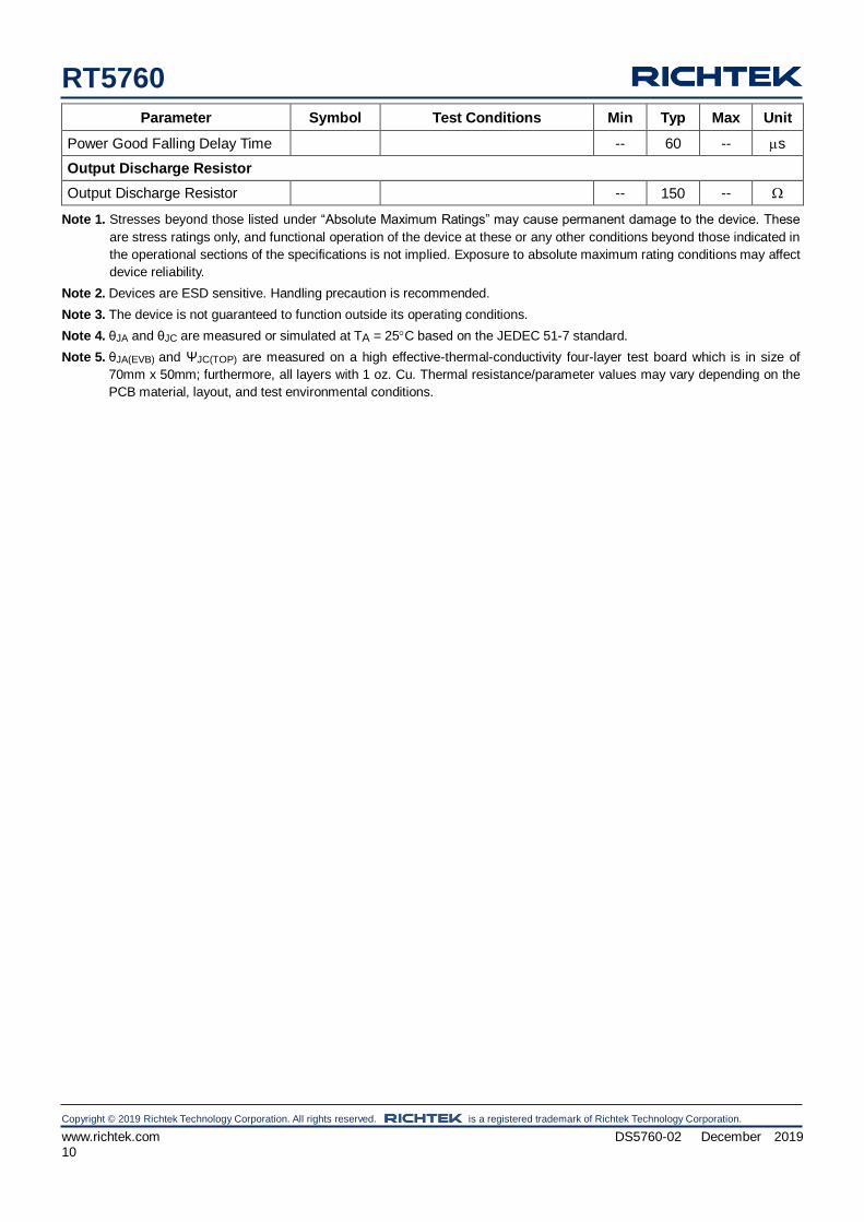
Power Good Falling Delay Time -- 60 -- s
Output Discharge Resistor
Output Discharge Resistor -- 150 --
Note 1. Stresses beyond those listed under “Absolute Maximum Ratings” may cause permanent damage to the device. These
are stress ratings only, and functional operation of the device at these or any other conditions beyond those indicated in
the operational sections of the specifications is not implied. Exposure to absolute maximum rating conditions may affect
device reliability.
Note 2. Devices are ESD sensitive. Handling precaution is recommended.
Note 3. The device is not guaranteed to function outside its operating conditions.
Note 4. θJA and θJC are measured or simulated at TA = 25C based on the JEDEC 51-7 standard.
Note 5. θJA(EVB) and ΨJC(TOP) are measured on a high effective-thermal-conductivity four-layer test board which is in size of
70mm x 50mm; furthermore, all layers with 1 oz. Cu. Thermal resistance/parameter values may vary depending on the
PCB material, layout, and test environmental conditions.

RT5760
Copyright © 2019 Richtek Technology Corporation. All rights reserved. is a registered trademark of Richtek Technology Corporation.
DS5760-02 December 2019 www.richtek.com 11
Typical Application Circuit
*CFF : Optional for performance fine-tune
**PG : RT5760A/B only.
EN
RT5760
FBGND
VINVIN
10μF
CIN
**PG
L
COUT
SW VOUT
RFB1
3
5
2
4
6
1
Enable
CIN
0.1μF
RFB2
*CFF10μF
VPG
100kRPG
Table 1. Suggested Component Values
VOUT (V) RFB1 (k) RFB2 (k) L (H)
3.3 45 10 1
1.8 20 10 1
1.5 15 10 1
1.2 10 10 1
1.05 7.5 10 1
1 6.65 10 1
Table 2. Recommended External Components
Component Description Vendor P/N
CIN 10F, 6.3V, X5R, 0603 0603X106M6R3 (WALSIN)
GRM188R60J106ME84 (MURATA)
*COUT 10F, 6.3V, X5R, 0603 0603X106M6R3 (WALSIN)
GRM188R60J106ME84 (MURATA)
L 1H DFE252010F-1R0M (MURATA)
HMLQ25201T-1R0MSR (CYNTEC)
*COUT : Considering the effective capacitance de-rated with biased voltage level and size, the COUT component
needs satisfy the effective capacitance at least 4F for VOUT = 3.3V and 7F for VOUT 3.3V for stable and
normal operation.
RT5760
Copyright © 2019 Richtek Technology Corporation. All rights reserved. is a registered trademark of Richtek Technology Corporation.
www.richtek.com DS5760-02 December 2019 12
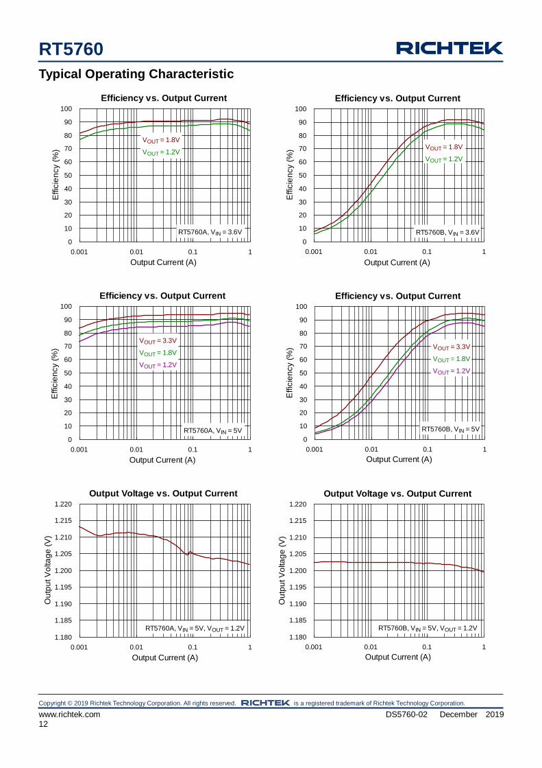
Typical Operating Characteristic
Efficiency vs. Output Current
0
10
20
30
40
50
60
70
80
90
100
0.001 0.01 0.1 1
Output Current (A)
Effic
ien
cy (
%)
VOUT = 1.8V
VOUT = 1.2V
RT5760A, VIN = 3.6V
Efficiency vs. Output Current
0
10
20
30
40
50
60
70
80
90
100
0.001 0.01 0.1 1
Output Current (A)
Effic
ien
cy (
%)
RT5760B, VIN = 3.6V
VOUT = 1.8V
VOUT = 1.2V
Efficiency vs. Output Current
0
10
20
30
40
50
60
70
80
90
100
0.001 0.01 0.1 1
Output Current (A)
Effic
ien
cy (
%)
VOUT = 3.3V
VOUT = 1.8V
VOUT = 1.2V
RT5760A, VIN = 5V
Efficiency vs. Output Current
0
10
20
30
40
50
60
70
80
90
100
0.001 0.01 0.1 1
Output Current (A)
Effic
ien
cy (
%)
RT5760B, VIN = 5V
VOUT = 3.3V
VOUT = 1.8V
VOUT = 1.2V
Output Voltage vs. Output Current
1.180
1.185
1.190
1.195
1.200
1.205
1.210
1.215
1.220
0.001 0.01 0.1 1
Output Current (A)
Ou
tpu
t V
olta
ge
(V
)
RT5760A, VIN = 5V, VOUT = 1.2V
Output Voltage vs. Output Current
1.180
1.185
1.190
1.195
1.200
1.205
1.210
1.215
1.220
0.001 0.01 0.1 1
Output Current (A)
Ou
tpu
t V
olta
ge
(V
)
RT5760B, VIN = 5V, VOUT = 1.2V
RT5760
Copyright © 2019 Richtek Technology Corporation. All rights reserved. is a registered trademark of Richtek Technology Corporation.
DS5760-02 December 2019 www.richtek.com 13
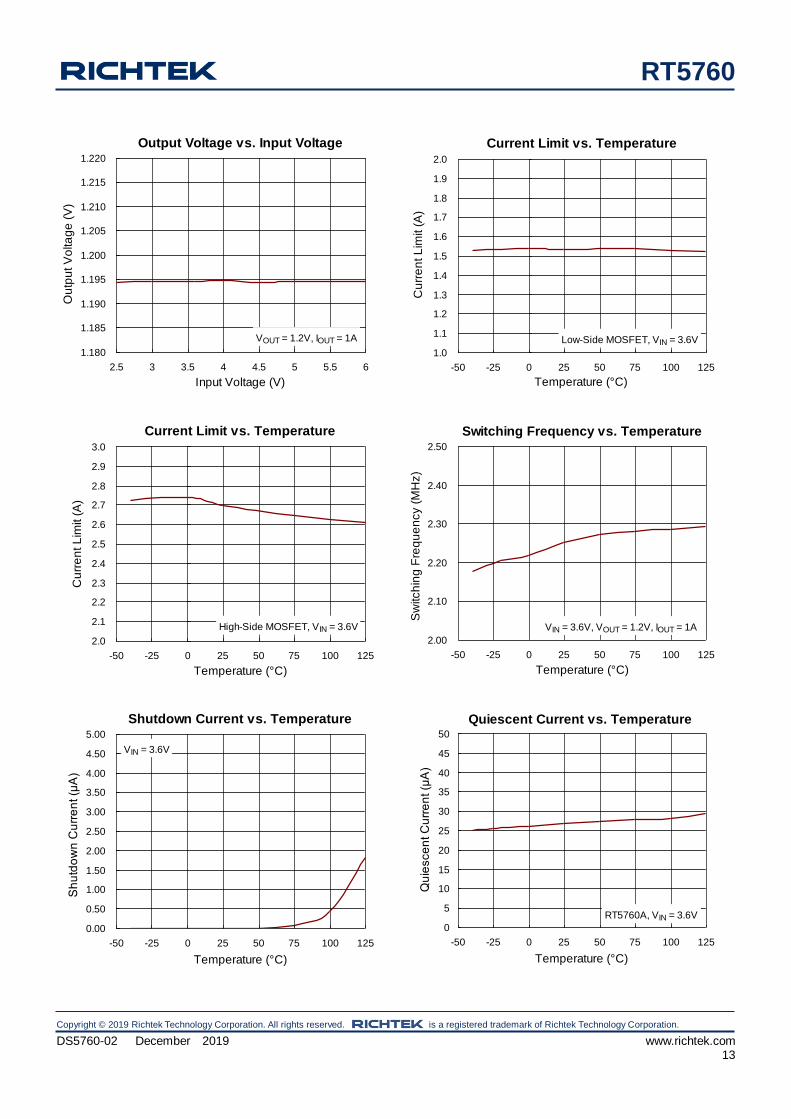
Output Voltage vs. Input Voltage
1.180
1.185
1.190
1.195
1.200
1.205
1.210
1.215
1.220
2.5 3 3.5 4 4.5 5 5.5 6
Input Voltage (V)
Ou
tpu
t V
olta
ge
(V
)
VOUT = 1.2V, IOUT = 1A
Current Limit vs. Temperature
1.0
1.1
1.2
1.3
1.4
1.5
1.6
1.7
1.8
1.9
2.0
-50 -25 0 25 50 75 100 125
Temperature (°C)
Cu
rre
nt L
imit (
A)
Low-Side MOSFET, VIN = 3.6V
Current Limit vs. Temperature
2.0
2.1
2.2
2.3
2.4
2.5
2.6
2.7
2.8
2.9
3.0
-50 -25 0 25 50 75 100 125
Temperature (°C)
Cu
rre
nt L
imit (
A)
High-Side MOSFET, VIN = 3.6V
Switching Frequency vs. Temperature
2.00
2.10
2.20
2.30
2.40
2.50
-50 -25 0 25 50 75 100 125
Temperature (°C)
Sw
itch
ing
Fre
qu
en
cy (
MH
z) 1
VIN = 3.6V, VOUT = 1.2V, IOUT = 1A
Shutdown Current vs. Temperature
0.00
0.50
1.00
1.50
2.00
2.50
3.00
3.50
4.00
4.50
5.00
-50 -25 0 25 50 75 100 125
Temperature (°C)
Sh
utd
ow
n C
urr
en
t (μ
A) 1
VIN = 3.6V
Quiescent Current vs. Temperature
0
5
10
15
20
25
30
35
40
45
50
-50 -25 0 25 50 75 100 125
Temperature (°C)
Qu
iesce
nt C
urr
en
t (μ
A)
RT5760A, VIN = 3.6V
RT5760
Copyright © 2019 Richtek Technology Corporation. All rights reserved. is a registered trademark of Richtek Technology Corporation.
www.richtek.com DS5760-02 December 2019 14
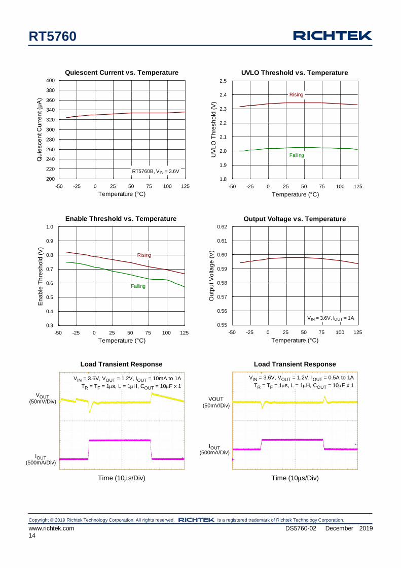
Quiescent Current vs. Temperature
200
220
240
260
280
300
320
340
360
380
400
-50 -25 0 25 50 75 100 125
Temperature (°C)
Qu
iesce
nt C
urr
en
t (μ
A)
RT5760B, VIN = 3.6V
UVLO Threshold vs. Temperature
1.8
1.9
2.0
2.1
2.2
2.3
2.4
2.5
-50 -25 0 25 50 75 100 125
Temperature (°C)
UV
LO
Th
resh
old
(V
)
Falling
Rising
Enable Threshold vs. Temperature
0.3
0.4
0.5
0.6
0.7
0.8
0.9
1.0
-50 -25 0 25 50 75 100 125
Temperature (°C)
En
ab
le T
hre
sh
old
(V
)
Rising
Falling
Output Voltage vs. Temperature
0.55
0.56
0.57
0.58
0.59
0.60
0.61
0.62
-50 -25 0 25 50 75 100 125
Temperature (°C)
Ou
tpu
t V
olta
ge
(V
)
VIN = 3.6V, IOUT = 1A
VIN = 3.6V, VOUT = 1.2V, IOUT = 10mA to 1A
TR = TF = 1s, L = 1H, COUT = 10F x 1
VOUT(50mV/Div)
IOUT(500mA/Div)
Time (10s/Div)
Load Transient Response
VIN = 3.6V, VOUT = 1.2V, IOUT = 0.5A to 1A
TR = TF = 1s, L = 1H, COUT = 10F x 1
VOUT
(50mV/Div)
IOUT (500mA/Div)
Time (10s/Div)
Load Transient Response

RT5760
Copyright © 2019 Richtek Technology Corporation. All rights reserved. is a registered trademark of Richtek Technology Corporation.
DS5760-02 December 2019 www.richtek.com 15
VIN = 3.6V, VOUT = 1.2V, IOUT = 10mA
VOUT(10mV/Div)
VSW(3V/Div)
Time (5s/Div)
Output Ripple Voltage
VIN = 3.6V, VOUT = 1.2V, IOUT = 1A
VOUT(10mV/Div)
VSW(3V/Div)
Time (200ns/Div)
Output Ripple Voltage
VIN = 3.6V, VOUT = 1.2V, IOUT = 1A
VOUT(500mV/Div
VSW (5V/Div)
VEN (2V/Div)
VPG (1V/Div)
Time (500s/Div)
Power On from EN
VIN = 3.6V, VOUT = 1.2V, IOUT = 1A
VOUT (500mV/Div)
VSW (5V/Div)
VEN (2V/Div)
VPG (1V/Div)
Time (10s/Div)
Power Off from EN
VIN = 3.6V, VOUT = 1.2V, IOUT = 1A
VOUT
(500mV/Div)
VSW (5V/Div)
VIN (2V/Div)
VPG (1V/Div)
Time (500s/Div)
Power On from VIN
VIN = 3.6V, VOUT = 1.2V, IOUT = 1A
VOUT (500mV/Div)
VSW (5V/Div)
VIN (2V/Div)
VPG (1V/Div)
Time (200s/Div)
Power Off from VIN

RT5760
Copyright © 2019 Richtek Technology Corporation. All rights reserved. is a registered trademark of Richtek Technology Corporation.
www.richtek.com DS5760-02 December 2019 16
Application Information
The output stage of a synchronous buck converter is
composed of an inductor and capacitor, which stores
and delivers energy to the load, and forms a
second-order low-pass filter to smooth out the switch
node voltage to maintain a regulated output voltage.
Inductor Selection
The inductor selection trade-offs among size, cost,
efficiency, and transient response requirements.
Generally, three key inductor parameters are specified
for operation with the device: inductance value (L),
inductor saturation current (ISAT), and DC resistance
(DCR).
A good compromise between size and loss is to choose
the peak-to-peak ripple current equals to 20% to 50%
of the IC rated current. The switching frequency, input
voltage, output voltage, and selected inductor ripple
current determines the inductor value as follows :
OUT IN OUT
IN SW L
V V VL =
V f I
Once an inductor value is chosen, the ripple current
(IL) is calculated to determine the required peak
inductor current.
OUT IN OUT LL L(PEAK) OUT(MAX)
IN SW
V V V II = and I = I
V f L 2
IL(PEAK) should not exceed the minimum value of IC's
upper current limit level. Besides, the current flowing
through the inductor is the inductor ripple current plus
the output current. During power up, faults or transient
load conditions, the inductor current can increase above
the calculated peak inductor current level calculated
above. In transient conditions, the inductor current can
increase up to the switch current limit of the device. For
this reason, the most conservative approach is to
specify an inductor with a saturation current rating equal
to or greater than the switch current limit rather than the
peak inductor current.
Considering the Typical Application Circuit for 1.2V
output at 1A and an input voltage of 5V, using an
inductor ripple of 0.4A (40% of the IC rated current), the
calculated inductance value is :
1.2 5 1.2L 1μH
5 2.2MHz 0.4A
For the typical application, a standard inductance value
of 1H can be selected.
L
1.2 5 1.2I = = 0.41A (41% of the IC rated current)
5 2.2MHz 1μH
L(PEAK)0.41A
and I = 1A + = 1.205A2
For the 1H value, the inductor's saturation and
thermal rating should exceed at least 1.205A. For more
conservative, the rating for inductor saturation current
must be equal to or greater than switch current limit of
the device rather than the inductor peak current.
For EMI sensitive application, choosing shielding type
inductor is preferred.
Input Capacitor Selection
Input capacitance, CIN, is needed to filter the pulsating
current at the drain of the high-side power MOSFET.
CIN should be sized to do this without causing a large
variation in input voltage. The waveform of CIN ripple
voltage and ripple current are shown in Figure 5. The
peak-to-peak voltage ripple on input capacitor can be
estimated as equation below :
CIN OUT OUTIN SW
1 DV = D I + I ESR
C f
Where
OUT
IN
VD =
V
For ceramic capacitors, the equivalent series
resistance (ESR) is very low, the ripple which is caused
by ESR can be ignored, and the minimum input
capacitance can be estimated as equation below :
IN_MIN OUT_MAX
CIN_MAX SW
D 1 DC I
V f =
CIN_MAXWhere mV 100 V

RT5760
Copyright © 2019 Richtek Technology Corporation. All rights reserved. is a registered trademark of Richtek Technology Corporation.
DS5760-02 December 2019 www.richtek.com 17
CIN Ripple Current
CIN Ripple Voltage VCIN
(1-D) x IOUT
D x IOUT
(1-D) x tSWD x tSW
VESR = IOUT x ESR
Figure 5. CIN Ripple Voltage and Ripple Current
In addition, the input capacitor needs to have a very
low ESR and must be rated to handle the worst-case
RMS input current of :
OUT INRMS OUT_MAX
IN OUT
V VI I 1
V V
It is commonly to use the worse IRMS IOUT/2 at VIN =
2VOUT for design. Note that ripple current ratings from
capacitor manufacturers are often based on only 2000
hours of life which makes it advisable to further de-rate
the capacitor, or choose a capacitor rated at a higher
temperature than required.
Several capacitors may also be paralleled to meet size,
height and thermal requirements in the design. For low
input voltage applications, sufficient bulk input
capacitance is needed to minimize transient effects
during output load changes.
Ceramic capacitors are ideal for switching regulator
applications due to its small, robust and very low ESR.
However, care must be taken when these capacitors
are used at the input. A ceramic input capacitor
combined with trace or cable inductance forms a high
quality (under damped) tank circuit. If the RT5760
circuit is plugged into a live supply, the input voltage
can ring to twice its nominal value, possibly exceeding
the device’s rating. This situation is easily avoided by
placing the low ESR ceramic input capacitor in parallel
with a bulk capacitor with higher ESR to damp the
voltage ringing.
The input capacitor should be placed as close as
possible to the VIN pins, with a low inductance
connection to the GND of the IC. In addition to a larger
bulk capacitor, a small ceramic capacitors of 0.1F
should be placed close to the VIN and GND pin. This
capacitor should be 0402 or 0603 in size.
Output Capacitor Selection
The RT5760 are optimized for ceramic output capacitors
and best performance will be obtained using them. The
total output capacitance value is usually determined by
the desired output voltage ripple level and transient
response requirements for sag (undershoot on load
apply) and soar (overshoot on load release).
Output Ripple
The output voltage ripple at the switching frequency is
a function of the inductor current ripple going through
the output capacitor’s impedance. To derive the output
voltage ripple, the output capacitor with capacitance,
COUT, and its equivalent series resistance, RESR, must
be taken into consideration. The output peak-to-peak
ripple voltage VRIPPLE, caused by the inductor current
ripple IL, is characterized by two components, which
are ESR ripple VRIPPLE(ESR) and capacitive ripple
VRIPPLE(C), can be expressed as below :
RIPPLE RIPPLE(ESR) RIPPLE(C)
RIPPLE(ESR) L ESR
LRIPPLE(C)
OUT SW
V = V V
V = I R
IV =
8 C f
If ceramic capacitors are used as the output capacitors,
both the components need to be considered due to the
extremely low ESR and relatively small capacitance.
For the RT5760’s Typical Application Circuit for output
voltage of 1.2V, and actual inductor current ripple (IL)
of 0.41A, taking a 10F ceramic capacitors of
GRM188R60J106ME84 from Murata as example, the
output ripple of the output capacitor is as below :
The ripple caused by the ESR of about 5m can be
calculated as
RIPPLE ESRV = 0.41A 5m = 2.05mV
Due to DC bias capacitance degrading, the effective
capacitance at output voltage of 1.2V is about 8F
RIPPLE C
RIPPLE
0.41AV = = 2.91mV
8 8μF 2.2MHz
V = 2.05mV + 2.91mV = 4.96mV
RT5760
Copyright © 2019 Richtek Technology Corporation. All rights reserved. is a registered trademark of Richtek Technology Corporation.
www.richtek.com DS5760-02 December 2019 18
Output Transient Undershoot and Overshoot
In addition to voltage ripple at the switching frequency,
the output capacitor and its ESR also affect the voltage
sag (undershoot) and soar (overshoot) when the load
steps up and down abruptly. The ACOTTM transient
response is very quick and output transients are
usually small. The following section shows how to
calculate the worst-case voltage swings in response to
very fast load steps.
The output voltage transient undershoot and overshoot
each have two components : the voltage steps caused
by the output capacitor's ESR, and the voltage sag and
soar due to the finite output capacitance and the
inductor current slew rate. Use the following formulas
to check if the ESR is low enough (typically not a
problem with ceramic capacitors) and the output
capacitance is large enough to prevent excessive sag
and soar on very fast load step edges, with the chosen
inductor value.
The amplitude of the ESR step up or down is a function
of the load step and the ESR of the output capacitor :
VESR _STEP = IOUT x RESR
The amplitude of the capacitive sag is a function of the
load step, the output capacitor value, the inductor value,
the input-to-output voltage differential, and the
maximum duty cycle. The maximum duty cycle during a
fast transient is a function of the on-time and the
minimum off-time since the ACOTTM control scheme
will ramp the current using on-times spaced apart with
minimum off-times, which is as fast as allowed.
Calculate the approximate on-time (neglecting
parasites) and maximum duty cycle for a given input
and output voltage as :
OUT ONON MAX
IN SW ON OFF_MIN
V tt = and D =
V f t t
The actual on-time will be slightly longer as the IC
compensates for voltage drops in the circuit, but we
can neglect both of these since the on-time increase
compensates for the voltage losses. Calculate the
output voltage sag as :
2OUT
SAGOUT IN(MIN) MAX OUT
L ( I )V =
2 C V D V
The amplitude of the capacitive soar is a function of the
load step, the output capacitor value, the inductor value
and the output voltage :
2OUT
SOAROUT OUT
L ( I )V =
2 C V
Due to some modern digital loads can exhibit nearly
instantaneous load changes, the amplitude of the ESR
step up or down should be taken into consideration.
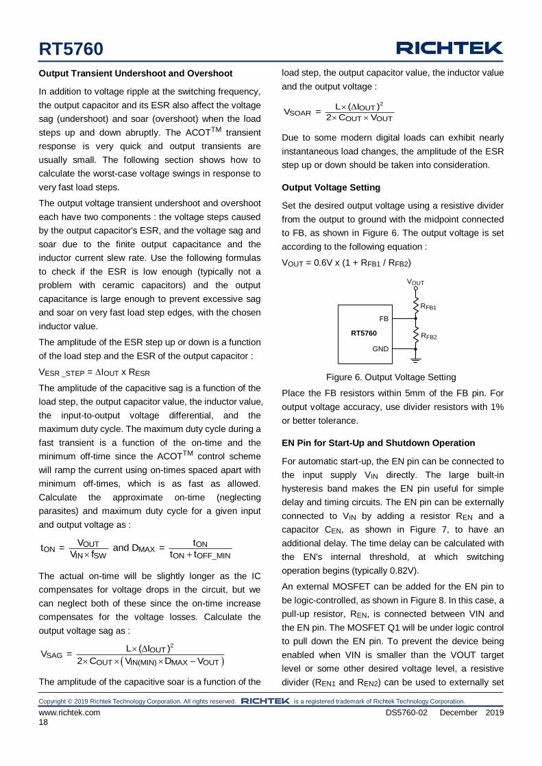
Output Voltage Setting
Set the desired output voltage using a resistive divider
from the output to ground with the midpoint connected
to FB, as shown in Figure 6. The output voltage is set
according to the following equation :
VOUT = 0.6V x (1 + RFB1 / RFB2)
RT5760
GND
FB
RFB1
VOUT
RFB2
Figure 6. Output Voltage Setting
Place the FB resistors within 5mm of the FB pin. For
output voltage accuracy, use divider resistors with 1%
or better tolerance.
EN Pin for Start-Up and Shutdown Operation
For automatic start-up, the EN pin can be connected to
the input supply VIN directly. The large built-in
hysteresis band makes the EN pin useful for simple
delay and timing circuits. The EN pin can be externally
connected to VIN by adding a resistor REN and a
capacitor CEN, as shown in Figure 7, to have an
additional delay. The time delay can be calculated with
the EN's internal threshold, at which switching
operation begins (typically 0.82V).
An external MOSFET can be added for the EN pin to
be logic-controlled, as shown in Figure 8. In this case, a
pull-up resistor, REN, is connected between VIN and
the EN pin. The MOSFET Q1 will be under logic control
to pull down the EN pin. To prevent the device being
enabled when VIN is smaller than the VOUT target
level or some other desired voltage level, a resistive
divider (REN1 and REN2) can be used to externally set

RT5760
Copyright © 2019 Richtek Technology Corporation. All rights reserved. is a registered trademark of Richtek Technology Corporation.
DS5760-02 December 2019 www.richtek.com 19
the input under-voltage lockout threshold, as shown in
Figure 9.
EN
GND
VIN
REN
CEN
RT5760
Figure 7. Enable Timing Control
EN
GND
VIN
REN
Q1Enable RT5760
Figure 8. Logic Control for the EN Pin
EN
GND
VIN
REN1
REN2RT5760
Figure 9. Resistive Divider for Under-Voltage Lockout
Threshold Setting
Power-Good Output
The PGOOD pin is an open-drain power-good
indication output and is to be connected to an external
voltage source through a pull-up resistor.
The external voltage source can be an external voltage
supply below 6V, VCC or the output of the RT5760 if the
output voltage is regulated under 6V. It is
recommended to connect a 100k between external
voltage source to PGOOD pin.
Thermal Considerations
The junction temperature should never exceed the
absolute maximum junction temperature TJ(MAX), listed
under Absolute Maximum Ratings, to avoid permanent
damage to the device. The maximum allowable power
dissipation depends on the thermal resistance of the IC
package, the PCB layout, the rate of surrounding airflow,
and the difference between the junction and ambient
temperatures. The maximum power dissipation can be
calculated using the following formula :
PD(MAX) = (TJ(MAX) TA) / JA
where TJ(MAX) is the maximum junction temperature, TA
is the ambient temperature, and JA is the
junction-to-ambient thermal resistance.
For continuous operation, the maximum operating
junction temperature indicated under Recommended
Operating Conditions is 125C. The junction-to-ambient
thermal resistance, JA, is highly package dependent.
For a SOT-563 (FC) package, the thermal resistance,
JA, is 100C/W on a high effective-thermal-conductivity
four-layer test board. The maximum power dissipation at
TA = 25C can be calculated as below :
PD(MAX) = (125C 25C) / (100C/W) = 1W for a
SOT-563 (FC) package.
The maximum power dissipation depends on the
operating ambient temperature for the fixed TJ(MAX) and
the thermal resistance, JA. The derating curves in
Figure 10 allows the designer to see the effect of rising
ambient temperature on the maximum power
dissipation.
Figure 10. Derating Curve of Maximum Power
Dissipation
Layout Considerations
Follow the PCB layout guidelines for optimal
performance of the device.
Keep the high-current paths short, especially at the
ground terminals. This practice is essential for stable,
jitter-free operation. The high current path
comprising of input capacitor, high-side FET,
inductor, and the output capacitor should be as short
0.0
0.2
0.4
0.6
0.8
1.0
1.2
1.4
1.6
0 25 50 75 100 125
Ambient Temperature (°C)
Ma
xim
um
Po
we
r D
issip
atio
n (
W) 1 Four-Layer PCB

RT5760
Copyright © 2019 Richtek Technology Corporation. All rights reserved. is a registered trademark of Richtek Technology Corporation.
www.richtek.com DS5760-02 December 2019 20
as possible. This practice is essential for high
efficiency.
Place the input MLCC capacitors as close to the VIN
and GND pins as possible. The major MLCC
capacitors should be placed on the same layer as
the RT5760.
SW node is with high frequency voltage swing and
should be kept at small area. Keep analog
components away from the SW node to prevent
stray capacitive noise pickup.
Connect feedback network behind the output
capacitors. Place the feedback components next to
the FB pin.
For better thermal performance, to design a wide
and thick plane for GND pin or to add a lot of vias to
GND plane.
An example of PCB layout guide is shown from Figure
11.
RT5760
Copyright © 2019 Richtek Technology Corporation. All rights reserved. is a registered trademark of Richtek Technology Corporation.
DS5760-02 December 2019 www.richtek.com 21
RFB2
RF
B1
CF
F
RP
G
CIN2
CIN1
COUT
L
REN
VOUT
VOUT
EN
GND GND
GND
GND
Place the input MLCC capacitors as
close to the VIN and GND pins as
possible.
Place the feedback components
next to the FB pin.
Connect feedback network
behind the output
Add extra vias for thermal dissipation
Keep analog components
away from the SW node to
prevent stray capacitive noise
pickup.
The VIN trace should have enough
width, and use several vias to
shunt the high input current.
FB
GN
DV
IN
PG
EN
SW 4
23
56 1
Figure 11. Layout Guide

RT5760
Copyright © 2019 Richtek Technology Corporation. All rights reserved. is a registered trademark of Richtek Technology Corporation.
www.richtek.com DS5760-02 December 2019 22
Outline Dimension
Symbol Dimensions In Millimeters Dimensions In Inches
Min Max Min Max
A 0.500 0.600 0.020 0.024
A1 0.000 0.050 0.000 0.002
A3 0.080 0.180 0.003 0.007
b 0.150 0.300 0.006 0.012
D 1.500 1.700 0.059 0.067
E 1.500 1.700 0.059 0.067
E1 1.100 1.300 0.043 0.051
e 0.500 0.020
L 0.100 0.300 0.004 0.012
L1 0.200 0.400 0.008 0.016
SOT-563 (FC) Surface Mount Package
RT5760
Copyright © 2019 Richtek Technology Corporation. All rights reserved. is a registered trademark of Richtek Technology Corporation.
DS5760-02 December 2019 www.richtek.com 23
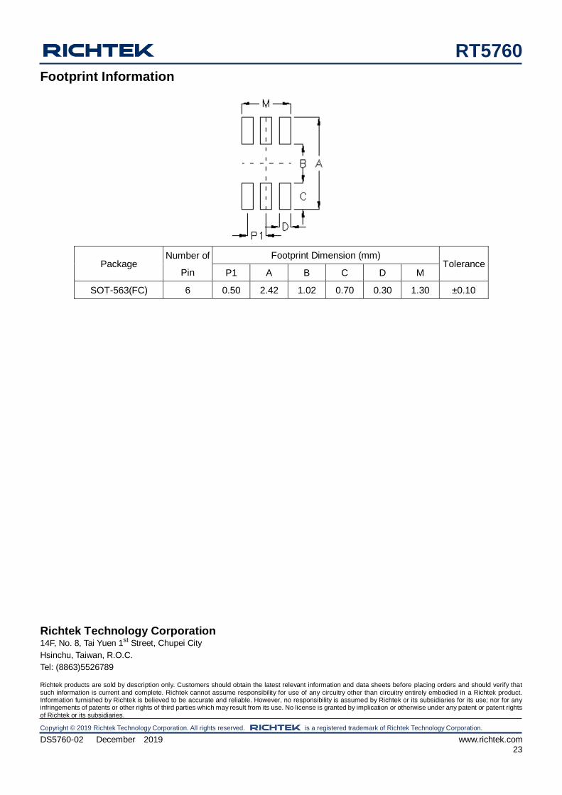
Footprint Information
Package Number of
Pin
Footprint Dimension (mm) Tolerance
P1 A B C D M
SOT-563(FC) 6 0.50 2.42 1.02 0.70 0.30 1.30 ±0.10
Richtek Technology Corporation 14F, No. 8, Tai Yuen 1st Street, Chupei City
Hsinchu, Taiwan, R.O.C.
Tel: (8863)5526789 Richtek products are sold by description only. Customers should obtain the latest relevant information and data sheets before placing orders and should verify that such information is current and complete. Richtek cannot assume responsibility for use of any circuitry other than circuitry entirely embodied in a Richtek product. Information furnished by Richtek is believed to be accurate and reliable. However, no responsibility is assumed by Richtek or its subsidiaries for its use; nor for any infringements of patents or other rights of third parties which may result from its use. No license is granted by implication or otherwise under any patent or patent rights of Richtek or its subsidiaries.
Recommended