Embed Size (px)
Citation preview
ISTFA 2012
Conference Proceedings from the 38th International Symposium for
Testing and Failure Analysis
November 11–15, 2012
Phoenix Convention Center Phoenix, Arizona, USA
Sponsored by
www.asminternational.org/istfa www.asminternational.org
TM
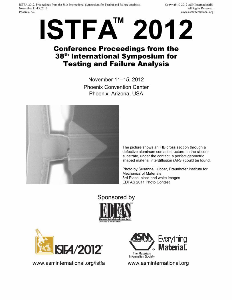
The picture shows an FIB cross section through a defective aluminum contact structure. In the silicon-substrate, under the contact, a perfect geometric shaped material interdiffusion (Al-Si) could be found. Photo by Susanne Hübner, Fraunhofer Institute for Mechanics of Materials 3rd Place: black and white images EDFAS 2011 Photo Contest
ISTFA 2012, Proceedings from the 38th International Symposium for Testing and Failure Analysis, November 11-15, 2012 Phoenix, AZ
Copyright © 2012 ASM International® All Rights Reserved.
www.asminternational.org
Copyright © 2012 by
ASM International® All rights reserved
No part of this book may be reproduced, stored in a retrieval system, or transmitted, in any form or by any means, electronic, mechanical, photocopying, recording, or otherwise, without the written permission of the copyright owner.
First printing, November 2012
Great care is taken in the compilation and production of this Volume, but it should be made clear that NO WARRANTIES, EXPRESS OR IMPLIED, INCLUDING, WITHOUT LIMITATION, WARRANTIES OF MERCHANTABILITY OR FITNESS FOR A PARTICULAR PURPOSE, ARE GIVEN IN CONNECTION WITH THIS PUBLICATION. Although this information is believed to be accurate by ASM, ASM cannot guarantee that favorable results will be obtained from the use of this publication alone. This publication is intended for use by persons having technical skill, at their sole discretion and risk. Since the conditions of product or material use are outside of ASM's control, ASM assumes no liability or obligation in connection with any use of this information. No claim of any kind, whether as to products or information in this publication, and whether or not based on negligence, shall be greater in amount than the purchase price of this product or publication in respect of which damages are claimed. THE REMEDY HEREBY PROVIDED SHALL BE THE EXCLUSIVE AND SOLE REMEDY OF BUYER, AND IN NO EVENT SHALL EITHER PARTY BE LIABLE FOR SPECIAL, INDIRECT OR CONSEQUENTIAL DAMAGES WHETHER OR NOT CAUSED BY OR RESULTING FROM THE NEGLIGENCE OF SUCH PARTY. As with any material, evaluation of the material under end-use conditions prior to specification is essential. Therefore, specific testing under actual conditions is recommended. Nothing contained in this book shall be construed as a grant of any right of manufacture, sale, use, or reproduction, in connection with any method, process, apparatus, product, composition, or system, whether or not covered by letters patent, copyright, or trademark, and nothing contained in this book shall be construed as a defense against any alleged infringement of letters patent, copyright, or trademark, or as a defense against liability for such infringement. Comments, criticisms, and suggestions are invited, and should be forwarded to ASM International.
ISBN-13:978-1-61503-979-1 ISBN-10: 1-61503-979-1
SAN: 204-7586
ASM International® Materials Park, OH 44073-0002
www.asminternational.org
Printed in the United States of America
iii
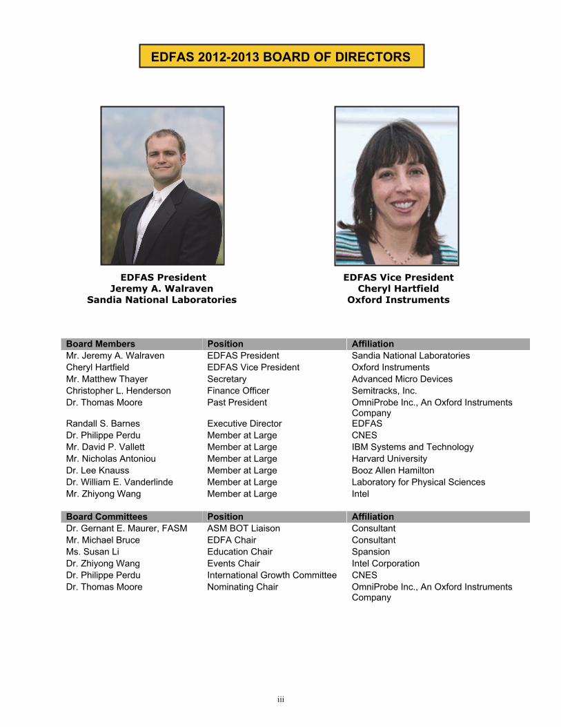
EDFAS 2012-2013 BOARD OF DIRECTORS
EDFAS President Jeremy A. Walraven
Sandia National Laboratories
EDFAS Vice President Cheryl Hartfield
Oxford Instruments
Board Members Position Affiliation Mr. Jeremy A. Walraven EDFAS President Sandia National Laboratories Cheryl Hartfield EDFAS Vice President Oxford Instruments Mr. Matthew Thayer Secretary Advanced Micro Devices Christopher L. Henderson Finance Officer Semitracks, Inc. Dr. Thomas Moore Past President OmniProbe Inc., An Oxford Instruments
Company Randall S. Barnes Executive Director EDFAS Dr. Philippe Perdu Member at Large CNES Mr. David P. Vallett Member at Large IBM Systems and Technology Mr. Nicholas Antoniou Member at Large Harvard University Dr. Lee Knauss Member at Large Booz Allen Hamilton Dr. William E. Vanderlinde Member at Large Laboratory for Physical Sciences Mr. Zhiyong Wang Member at Large Intel Board Committees Position Affiliation Dr. Gernant E. Maurer, FASM ASM BOT Liaison Consultant Mr. Michael Bruce EDFA Chair Consultant Ms. Susan Li Education Chair Spansion Dr. Zhiyong Wang Events Chair Intel Corporation Dr. Philippe Perdu International Growth Committee CNES Dr. Thomas Moore Nominating Chair OmniProbe Inc., An Oxford Instruments
Company
iv
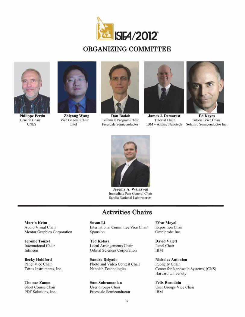
OORRGGAANNIIZZIINNGG CCOOMMMMIITTTTEEEE
Philippe Perdu Zhiyong Wang Dan Bodoh James J. Demarest Ed Keyes General Chair Vice General Chair Technical Program Chair Tutorial Chair Tutorial Vice Chair CNES Intel Freescale Semiconductor IBM – Albany Nanotech Solantro Semiconductor Inc.
Jeremy A. Walraven
Immediate Past General Chair Sandia National Laboratories
AAccttiivviittiieess CChhaaiirrss
Martin Keim Audio Visual Chair Mentor Graphics Corporation
Susan Li International Committee Vice Chair Spansion
Efrat Moyal Exposition Chair Omniprobe Inc.
Jerome Touzel International Chair Infineon
Ted Kolasa Local Arrangements Chair Orbital Sciences Corporation
David Valett Panel Chair IBM
Becky Holdford Panel Vice Chair Texas Instruments, Inc.
Sandra Delgado Photo and Video Contest Chair Nanolab Technologies
Nicholas Antoniou Publicity Chair Center for Nanoscale Systems, (CNS) Harvard University
Thomas Zanon Short Course Chair PDF Solutions, Inc.
Sam Subramanian User Groups Chair Freescale Semiconductor
Felix Beaudoin User Groups Vice Chair IBM
v
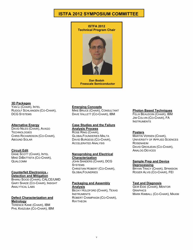
ISTFA 2012 SYMPOSIUM COMMITTEE
ISTFA 2012 Technical Program Chair
Dan Bodoh Freescale Semiconductor
3D Packages YAN LI (CHAIR), INTEL RUDOLF SCHLANGEN (CO-CHAIR), DCG SYSTEMS Alternative Energy DAVID NILES (CHAIR), AVAGO
TECHNOLOGIES CHRIS RICHARDSON (CO-CHAIR), ABOUND SOLAR Circuit Edit DANE SCOTT (CHAIR), INTEL MIKE DIBATTISTA (CO-CHAIR), QUALCOMM Counterfeit Electronics - Detection and Mitigation BHANU SOOD (CHAIR), CALCE/UMD GARY SHADE (CO-CHAIR), INSIGHT
ANALYTICAL LABS Defect Characterization and Metrology TERENCE KANE (CHAIR), IBM PHIL KASZUBA (CO-CHAIR), IBM
Emerging Concepts MIKE BRUCE (CHAIR), CONSULTANT DAVE VALLETT (CO-CHAIR), IBM Case Studies and the Failure Analysis Process ROSE RING (CHAIR), GLOBALFOUNDERIES MALTA DAVID BURGESS (CO-CHAIR), ACCELERATED ANALYSIS Nanoprobing and Electrical Characterization JOHN SANDERS (CHAIR), DCG
SYSTEMS CHRISTIAN HOBERT (CO-CHAIR), GLOBALFOUNDRIES Packaging and Assembly Analysis BECKY HOLDFORD (CHAIR), TEXAS
INSTRUMENTS ROBERT CHAMPAIGN (CO-CHAIR), RAYTHEON
Photon Based Techniques FELIX BEAUDOIN (CHAIR), IBM JIM COLVIN (CO-CHAIR), FA
INSTRUMENTS Posters MARTIN VERSEN (CHAIR), UNIVERSITY OF APPLIED SCIENCES
ROSENHEIM DAVID GROSJEAN (CO-CHAIR), ANALOG DEVICES Sample Prep and Device Deprocessing BRYAN TRACY (CHAIR), SPANSION ROGER ALVIS (CO-CHAIR), FEI Test and Diagnosis GEIR EIDE (CHAIR), MENTOR
GRAPHICS MARK KIMBALL (CO-CHAIR), MAXIM
vi
USER GROUPS
Nanoprobing Moderators Vijay Chowdhury EAGLABS Randal Mulder Silicon Laboratories Presentations
The Wonderful World of Atomic Force Probing (AFP) with Applications Examples, Its Limitations and Challenges Yuk Tsang Freescale Semiconductor, Austin, Texas, USA Advances in Nanoprobing Stephan Kleindiek Kleindiek Nanotechnik GmbH, Reutlingen, Germany Nanoprobe Sample Preparation and Probe Tip Issues Randal Mulder Silicon Laboratories, Austin, Texas, USA Sample Preparation Challenges and Techniques for FEOL Nanoprobing on Advanced Technology Nodes Sean Zumwalt Multiprobe Inc., Santa Barbara, CA, USA
vii
Contactless Fault Isolation Moderators Ed Cole Sandia National Labs Frank Altmann Fraunhofer Institute for Mechanics of Materials) Presentations Addressing 3D IC Challenges: Magnetic Field Imaging for Non‐Destructive 3D Fault Isolation Antonio Orozco Neocera, Beltsville, Maryland, USA The Benefits of Frequency Mapping Chris Nemirow DCG Systems, Fremont, California, USA A New Approach for Short Localization in Thin Dielectrics by Electron Beam Absorbed Current Imaging Michél Simon‐Najasek Fraunhofer CAM, Halle, Germany
Focused Ion Beam (FIB) Moderators Richard Livengood Intel Mike DiBattista Qualcomm Presentations
Rapid Laser Material Removal for Cross Sectional Imaging for 3D Pkg Level Analysis Jerry Lehman Zeiss Microscopy, Thornwood, NY, USA Multi Beam Plasma Xe/Ga FIB for Pkg & TSV FA Drew Erwin Tescan USA, Pleasanton, California, USA Developing Functional Prototypes by “Package Edit” Using Plasma FIB Technology Pete Carleson FEI, Hillsboro, Oregon, USA
viii
Next Generation Chemistry for Circuit Edit Hideo Tanaka DCG Systems, Fremont, California, USA 3D FIB/SEM at the 5 nm Voxel Scale for CE and Other IC Applications Mike Phaneuf Fibics Incorporated, Ottawa, Ontario, Canada
Sample Preparation Moderators Lucas Copeland Texas Instruments Jacob Klein Texas Instruments Presentations Etch Rate Characterization of Palladium (Pd) Coated Copper (Cu) Bond Wires Raymond Mendaros, Analog Devices General Trias (ADGT), Philippines EXpressLO™ for Routine Backside Milling Lucille A. Giannuzzi L.A. Giannuzzi & Associates LLC, Fort Myers, Florida, USA Safe Removal of WCSP/BGA Devices from Under‐Fill Applications Kristopher Staller Texas Instruments, Tucson, Arizona, USA Preparation of Wafer Level Packages Using Pulsed Laser Assisted Chemical Etching Scott Silerman, and Robert Chivas Varioscale, Inc, San Marcos, California, USA
ix
Contents
2012 IPFA Best Paper
Laser Voltage Probing in Failure Analysis of Advanced Integrated Circuits on SOI ...................................................................................... 1
V.K. Ravikumar1, R. Wampler2, M.Y. Ho1, J. Christensen2, S.L. Phoa1 1) Advanced Micro Devices Singapore Pte. Ltd., Singapore 2) Advanced Micro Devices, Inc., Austin, TX, USA
Session 1: Emerging Concepts and Techniques
Closer to the Theoretical Limit: Spherical Corrections to Aplanatic Solid Immersion Imaging with Adaptive Optics .................................................... 6
Y. Lu, E. Ramsay, C.R. Stockbridge, A. Yurt, F.H. Köklü, T.G. Bifano, M.S. Ünlü, and B.B. Goldberg, Boston University, Boston MA, USA
Fault Isolation of Open Defects Using Space Domain Reflectometry ................................. 11 Mayue Xie1, Zhiguo Qian1, Mario Pacheco1, Zhiyong Wang1, Rajen Dias1, and Vladimir Talanov2, 1) Intel Corporation, Chandler, AZ, USA 2) Neocera, LLC, Beltsville, MD, USA
Localization of Dead Open in a Solder Bump by Space Domain Reflectometry ................ 17
David P. Vallett1, Daniel A. Bader1, Vladimir V. Talanov2, Jan Gaudestad2, Nicolas Gagliolo2, and Antonio Orozco2 1) IBM Technology Group, Essex Junction, VT, USA 2) Neocera, LLC, Beltsville, MD, USA
Advanced Fault Isolation Technique Using Electro-Optical Terahertz Pulse Reflectometry (EOTPR) for 2D and 2.5D Flip-Chip Package ................................................ 21
Lihong Cao1, Manasa Venkata1, Meng Yeow Tay2, Wen Qiu2, J. Alton3, P. Taday3, and M. Igarashi3, 1) Advanced Micro Devices, Austin, TX, USA 2) Advanced Micro Devices (Singapore), Singapore 3)TeraView Limited, Cambridge, United Kingdom
Novel Plasma FIB/SEM for High Speed Failure Analysis and Real Time Imaging of Large Volume Removal ...................................................................... 26
T. Hrnčíř1, F. Lopour1, M. Zadražil1, A. Delobbe2, O. Salord2, and P. Sudraud2 1)TESCAN a.s., Brno, Czech Republic 2) Orsay Physics S.A., Fuveau, France
FemtoFarad/TeraOhm Endpoint Detection for Microsurgery of Integrated Circuit Devices ...................................................................................................... 30
Jim Colvin, Newark, CA, USA
x
Session 2: Fault Isolation and Failure Analysis of TSV
Cross Section Analysis of Cu Filled TSVs Based on High Throughput Plasma- FIB Milling .................................................................................... 39
Frank Altmann1, Jens Beyersdorfer1, Jan Schischka1, Michael Krause1, German Franz2, and Laurens Kwakman2 1) Fraunhofer Institute for Mechanics of Materials, Halle, Germany 2) FEI Europe B.V., Eindhoven, The Netherlands
Microstructural Considerations on the Reliability of 3D Packaging ................................... 44 Zhiheng Huang, Zhiyong Wu, Hua Xiong, and Yucheng Ma, Sun Yat-sen University, Guangzhou, China
High-Frequency TSV Failure Detection Method with Z Parameter ...................................... 50 Joohee Kim1, Daniel H. Jung1, Jonghyun Cho1, Jun So Pak1, Joungho Kim1, Jong Min Yook2, and Jun Chul Kim2 1) Korea Advanced Institute of Science and Technology, Deajeon, Republic of Korea 2) Korea Electronic Technology Institute, Gyeonggi-do, Republic of Korea
Enhanced Failure Analysis on Open TSV Interconnects ..................................................... 55 F. Altmann1, C. Schmidt1, J. Beyersdorfer1, M. Simon-Najasek1, C. Große1, F. Schrank2, and J. Kraft2 1) Fraunhofer-Institute for Mechanics of Materials, Halle, Germany 2) ams AG, Unterpremstaetten, Austria
Session 3: Nanoprobing Techniques A New Technique for Non-Invasive Short-Localisation in Thin Dielectric Layers by Electron Beam Absorbed Current (EBAC) Imaging .................. 61
Michél Simon-Najasek, Jörg Jatzkowski, Christian Große, and Frank Altmann, Fraunhofer Institute for Mechanics of Materials, Halle, Germany
Precise Localization of 28 nm via Chain Resistive Defect Using EBAC and Nanoprobing .......................................................................................................... 67
P. Larré1, H. Tupin1, C. Charles1, R.H. Newton2, and A. Reverdy3 1) STMicroelectronics, Crolles, France 2) DCG Systems Richardson, TX, USA 3) Sector Technology, Gières, France
In FAB 300 mm Wafer Level Atomic Force Probe Characterization .................................... 71
Terence Kane, IBM Systems Technology Group, Hopewell Junction, NY, USA Nanoelectronic Analog Circuit PFA – The Return of Circuit Level Probing ....................... 77
D.E. Albert, L. Fischer, and S. Beck, IBM, Hopewell Junction, NY, USA
xi
Session 4: Fault Isolation and Failure Analysis of 3D Packages Enhanced Comparison of Lock-In Thermography and Magnetic Microscopy for 3D Defect Localization of System in Packages .......................... 88
Christian Schmidt1, Frank Altmann1, and David P. Vallett2 1) Fraunhofer-Institute for Mechanics of Materials, Halle, Germany 2) IBM Systems & Technology Group, Essex Junction, VT, USA
Non Destructive Failure Analysis of 3D Electronic Packages Using Both Electro Optical Terahertz Pulse Reflectometry and 3D X-Ray Computed Tomography ......................................................................................... 95
Yan Li, Yongming Cai, Mario Pacheco, Rajen C. Dias, and Deepak Goyal, Intel Corporation, Chandler, AZ, USA
Failure Analysis Using Scanning Acoustic Microscopy for Diagnostics of Electronic Devices and 3D System Integration Technologies ............................................ 100
Peter Czurratis1, Peter Hoffrogge1, Sebastian Brand2, Frank Altmann2, and Matthias Petzold2 1) PVA Tepla Analytical Systems GmbH, Westhausen, Germany 2) Faunhofer Institute for Mechanics of Materials, Halle (Saale), Germany
Session 5: Nanoprobing Applications
Analysis of an Anomalous Transistor Exhibiting Dual-Vt Characteristics and Its Cause in a 90 nm Node CMOS Technology .................................................................... 106
Yuk L. Tsang, Xiang D. Wang, Reyhan Ricklefs, and Jason Goertz, Freescale Semiconductor Inc., Austin, TX, USA
Study of Static Noise Margin, Cell Stability and Influence of Electron Beam on Sub-30 nm SRAM Using SEM-Based Nanoprobing with 8 Nanoprobes ............................ 112
T.H. Ng, M.K. Dawood, P.K. Tan, H. Tan, C.K. Oh, J.C. Lam, and Z.H. Mai, GlobalFoundries Singapore Pte. Ltd., Singapore
Leaky Device Channel Anomaly Identification and Case Study by Nano-Probing Technique, Curve Fitting, and Model Analysis ............................................ 118
Wei-Chih Wang, Ching-Shan Sung, Ya-Hsiu Lin, Haw-Shan Chen, and Jian-Shing Luo, Inotera Memories, Inc., Taoyuan, Taiwan, Republic of China
Session 6: Photon Based Techniques: An Understanding
Photon Emission Spectra of FETs as Obtained by InGaAs Detector ................................. 123 Arkadiusz Glowacki1, Christian Boit1, Yoshiyuki Yokoyama2, and Philippe Perdu3 1) Berlin University of Technology, Berlin, Germany 2) Hamamatsu Photonics Germany, Herrsching, Germany 3) French Space Agency, Toulouse, France
xii
Near-Infrared Photon Emission Spectroscopy Trends in Scaled SOI Technologies ....................................................................................................... 128
Ulrike Kindereit1, Alan J. Weger1, Franco Stellari1, Peilin Song1, Hervé Deslandes2, Ted Lundquist2, and Prasad Sabbineni2 1) IBM T.J. Watson Research Center, Yorktown Heights, NY, USA 2) DCG Systems, Fremont, CA, USA
Characterization and TCAD Simulation of 90 nm Technology PMOS Transistor under Continuous Photoelectric Laser Stimulation for Failure Analysis Improvement ............................................................................................... 135
R. Llido1, A. Sarafianos1, O. Gagliano1, V. Serradeil1, V. Goubier1, M. Lisart1, G. Haller1, V. Pouget2, D. Lewis2, J.M. Dutertre3, and A. Tria3 1) STMicroelectronics, Rousset, France 2) University of Bordeaux, Talence, France 3) Centre de Microélectronique de Provence, Gardanne, France
Building the Electrical Model of the Photoelectric Laser Stimulation of an NMOS Transistor in 90 nm Technology ................................................................................ 143
A. Sarafianos1, R. Llido1, O. Gagliano1, V. Serradeil1, M. Lisart1, V. Goubier1, J.M. Dutertre2, A. Tria2, V. Pouget3, and D. Lewis3 1) STMicroelectronics, Rousset, France 2) Centre de Microélectronique de Provence - Georges Charpak, Gardanne, France 3) Université de Bordeaux, Talence, France
Session 7: Rethinking the FA Process Words for the “Whys” ............................................................................................................ 151
Richard J. Ross, Essex Junction, VT, USA EOS (Electrical Overstress) – The Old, Unknown Phenomenon? ...................................... 156
Peter Jacob, EMPA Duebendorf, Switzerland DRAM Cell Fault Localization Using Passive Voltage Contrast ......................................... 164
San Lin Liew, Yu Pei Wei, Bi Jen Chen, Hua Sheng Chen, and Jian Shing Luo, Inotera Memories Inc., Taoyuan, Taiwan, Republic of China
3D Tomography Analysis of Dark Voltage Contrast Failure in PCRAM Device ........................................................................................................................ 170
Jangwon Oh, Jonghyeop Kim, Taekwon Lee, Seungjoon Jeon, Won Kim, Hojoung Kim, and Changreol Kim, SK Hynix Semiconductor Inc., Kyoungki-do, Korea
Session 8: Photon Based Techniques: One Step Beyond
Dual-Phase Interferometric Confocal Imaging for Electrical Signal Modulation Mapping in ICs ........................................................................ 172
A. Yurt, E. Ramsay, F.H. Köklü, C.R. Stockbridge, Y. Lu, M.S. Ünlü, and B.B. Goldberg, Boston University, Boston, MA, USA
xiii
Laser Voltage Imaging: New Perspective Using Second Harmonic Detection on Submicron Technology .................................................... 176
Guillaume Celi1, Sylvain Dudit1, Thierry Parrassin1, Michel Vallet1, Philippe Perdu2, Antoine Reverdy3, and Dean Lewis4 1) STMicroelectronics, Crolles, France 2) CNES Laboratory, Toulouse, France 3) SECTOR Technologies, Gières, France 4) Université Bordeaux, Talence, France
Improving the DLS Workflow ................................................................................................. 183 Dan Bodoh and Kent Erington, Freescale Semiconductor, Austin, TX, USA
Differential Polarization Imaging and Probing [DPIP]: Seeing and Probing the “Invisible” ....................................................................................... 190
Baohua Niu, Martin von Haartman, Patrick Pardy, and Mitch Sacks, Intel Corporation, Hillsboro, OR, USA
Session 9: Technology Specific Case Studies
Advanced Physical Analysis Methodology for Yield and Reliability of 28-nm, Bulk-Si, Flip-Chip ICs Using SEM and Backside Deprocessing ............................ 197
Yuanjing (Jane) Li, Steven Scott, and Howard Lee Marks, NVIDIA Corporation, Santa Clara, CA, USA
A Comprehensive Failure Analysis Method and Mechanism Study on Ultra-Low-K Film Adhesion Failure ....................................................................................... 203
Shuting Chen, Lei Zhu, Han Wei Teo, Binghai Liu, Yanhua Huang, Kenny Ong, Zhiqiang Mo, Younan Hua, Zhaoxin Yuan, Yong Seng Heng, and Chao Yong Li, GlobalFoundries Singapore Pte. Ltd. Singapore
Systematic Approach for the Gate Oxide Failure Caused by Arsenic Cross Contamination ............................................................................................... 207
Lei Zhu, Huipeng Ng, Yanhua Huang, Hanwei Teo, Kenny Ong, Shuting Chen, Changqing Chen, Ghimboon Ang, Younan Hua, and Zheng Li, GlobalFoundries Singapore Pte. Ltd. Singapore
Failure Analysis on Integrated Power Devices .................................................................... 211 Arthur Chiang, David Le, and Huixian Wu, Vishay Siliconix, Santa Clara, CA, USA
Session 10: Photon Based Techniques: More Applications
Lock-in Phase Mapping of Modulated Reflectance in Dynamically Operating Mixed-Signal IC Devices ................................................................. 217
Zhongling Qian, Christof Brillert, and Christian Burmer, Infineon Technologies AG, Munich, Germany
xiv
Advanced Laser Probe Techniques Applied to FA of RF Integrated Circuits - A Case Study ......................................................................... 223
Mark Kimball1 and Christopher Nemirow2 1) Maxim Integrated Products, Inc. 2) DCG Systems
Case Study: Combined Dynamic Laser Stimulation and Static Emission Microscopy Techniques Applied to Scan Test Failure on Mixed Mode Device ............................................................................. 228
Magdalena Sienkiewicz and Philippe Rousseille, Freescale Semiconductor, Toulouse, France
From EBT to LVP, from 130 nm to 28 nm Node, Internal Timing Characterization Evolution .......................................................................... 232
Thierry Parrassin1, Philippe Larre1, Sylvain Dudit1, Michel Vallet1, and Antoine Reverdy2 1) STMicroelectronics,Crolles, France 2) SECTOR Technologies, Gières, France
Session 11: Alternative Energy
Lithium-Ion Battery Degradation Mechanisms and Failure Analysis Methodology ............................................................................................... 239
Bhanu Sood1, Lucas Severn1, Michael Osterman1, Michael Pecht1, Anton Bougaev2, and David McElfresh2 1) University of Maryland, College Park, MD, USA 2) Oracle Corporation, San Diego, CA, USA
Lock-In Thermography-Based Local Efficiency Analysis of Solar Cells ........................... 250 Otwin Breitenstein, Max Planck Institute of Microstructure Physics, Halle, Germany
Challenges for Parametric Analysis of the Solar Cells Using Failure Analysis Technique Developed for the Microelectronics ....................................... 255
M. Boostandoost, X. Ycaza, R. Leihkauf, U. Kerst, and C. Boit, Berlin University of Technology, Berlin, Germany
Session 12: Improving Fault Isolation with Software
Filtering and Emission Area Identification in the Time Resolved Imaging Data ................................................................................................. 264
S. Chef1, S. Jacquir1, S. Binczak1, K. Sanchez2, and P. Perdu2 1) University of Burgundy, Dijon, France 2) CNES, French Space Agency, Toulouse, France
Advanced Methods and Software for Enhancing Analytical Tools Capabilities during Chip Diagnostic and Characterization ................................................................................... 273
Franco Stellari and Peilin Song, IBM T.J. Watson Research Center, Yorktown Heights, NY, USA
xv
Improved Parasitic Fault Modeling for Automatic Analog Fault Simulation ..................... 281
Gerhard Borgmann, Christian Burmer, and Sébastien Mézière, Infineon Technologies AG, Munich, Germany
Time Resolved Imaging Solving FPGA Logic Fault Localization by Pattern Matching Technique .................................................................................................. 286
G. Bascoul1, P. Perdu1, and J. Di Battista2 1) Centre National d’Etudes Spatiales, Toulouse, France 2) Thales Communication and Security, Toulouse, France
Session 13: Defect Analysis SIMS Analysis for the Threshold Voltage Shift of Power MOS Caused by Abnormal Dopant Diffusion ........................................................... 290
Yanhua Huang1, Lei Zhu1, Kenny Ong1, Hanwei Teo1, Shuting Chen1, Younan Hua1, Miao Shen1, and Hao Gong2 1) GlobalFoundries Singapore Pte. Ltd., Singapore 2) National University of Singapore, Singapore
Study of Si Crystal Defects by Chemical Preferential Etching and Its Application on Si Dislocation Defects Caused by Laser Spike Annealing (LSA) ................................................................................................. 293
Shuting Chen, Lihong Li, Anyan Du, and Younan Hua, GlobalFoundries Singapore Pte. Ltd., Singapore
A Novel Integrated Reliability Test System for BEOL TDDB Study .................................... 297 Jifeng Chen, Peilin Song, Thomas M. Shaw, Franco Stellari, Lynne Gignac, Chris Breslin, Dirk Pfeiffer, and Griselda Bonila, IBM T.J. Watson Research Center, Yorktown Heights, NY, USA
Session 14: Packaging and Assembly Analysis
Fluorosilicate Glass (FSG) Outgassing Induced Aluminum Bond Pad Corrosion during Post-Fab Wafer Storage ....................................... 305
Younan Hua, Ramesh Rao Nistala, and Shuting Chen, GlobalFoundries Singapore Pte. Ltd., Singapore
An Overview of Cu Wire Intermetallic Compound Formation and a Corrosion Failure Mechanism ............................................................................................... 310
Dongmei Meng, Laura Buck, and James Cargo, LSI Corporation, Fort Collins, CO, USA Lock-in Thermography for Flip-Chip Package Failure Analysis ......................................... 316
Lihong Cao1, Manasa Venkata1, Jeffery Huynh1, Joseph Tan2, Meng-Yeow Tay2, Wen Qiu2, Kannu Wadhwa3, and Rudolf Schlangen3 1) Advanced Micro Devices, Austin, TX, USA 2) Advanced Micro Devices, Singapore 3) DCG Systems, Fremont, CA, USA
xvi
Dynamic Impact Package Characterization .......................................................................... 325 Jake E. Klein and Ronald R. Madsen, Texas Instruments, Tucson, AZ, USA
Development of Advanced Non Destructive Techniques for Failure Analysis of PCBs and PCBAs ................................................................................... 332
Julien Perraud1, Shaïma Enouz-Vedrenne1, Jean-Claude Clement1, and Arnaud Grivon2 1) Thales Research and Technology, Palaiseau, France 2) Thales Global Services, Meudon La Forêt, France
Session 15: TEM Defect Detection
Four Stages of Defect Creation in Epitaxial Structures: High Resolution X-Ray Diffraction and Transmission Electron Microscopy Characterization ......................................................... 337
Nikolai N. Faleev, Christiana B. Honsberg, and David J. Smith, Arizona State University, Tempe, AZ, USA
A Proof for the Possibility of Ce-Oxide from CMP Residuals in Si-Wafers by Analytical TEM .................................................................. 347
Wayne Zhao1, Liem Do Thanh1, Michael Gribelyuk2, Mary-Ann Zaitz2, and Wing Lai2 1) GlobalFoundries Inc., Hopewell Junction, NY, USA 2) IBM at Hopewell Junction, East Fishkill, NY, USA
Tomographic Study of Silicon Nanoparticles in Nanocrystalline Non-Volatile Flash Memory Devices by EFTEM ....................................... 356
YongKai Zhou, Jie Zhu, AnYan Du, YouNan Hua, ZhiQiang Mo, and SiPing Zhao, GlobalFoundries Singapore Pte. Ltd., Singapore
Energy-Filtered Imaging of Polysilicon Defects, Gate Dielectric and Silicon Nanocrystals Using Plasmon Energy-Loss Electrons ............................................ 359
Swaminathan Subramanian, Khiem Ly and Tony Chrastecky, Freescale Semiconductor Inc., Austin, TX, USA
Session 16: Case Studies I
Analysis of Fractures of Printed Circuit Board Traces ....................................................... 365 Carl Nail and Larry Rice, EAG, Irvine, CA, USA
Failure Analysis Methodology on Systematic Defect in N+ poly/NWELL Varactor in RF Analog_PLL due to Implanter Charging Issue ................ 370
Ghim Boon Ang, Changqing Chen, Hui Peng Ng, Soh Ping Neo, G. Magdeliza, Jony Indahwan, and Mern Tat Lee, GlobalFoundries Singapore Pte. Ltd., Singapore
Study on ATPG Failure with Butterfly Pattern ..................................................................... 375 C.Q. Chen, G.B. Ang, S.P. Zhao, S.P. Neo, A. Quah, Angela Teo, and B.H. Liu, GlobalFoundries Singapore Pte. Ltd., Singapore
xvii
Session 17: Device Level Sample Prep
Metallic Nanoneedles Arrays for TEM Sample Preparation “Lift-Out” ............................... 379 Romaneh Jalilian1, David Mudd1, Neil Torrez1, Jose Rivera1, Mehdi M. Yazdanpanah1, and Brian Miller2 1) NaugaNeedles, Louisville, KY, USA 2) Nanolab Technologies, Inc., Vancouver, W, USA
Deprocessing Methodologies for Detection of IBC and Cell-to-Cell Shorts in Submicron DRAM ............................................................................... 383
Ramachandra Chitakudige1, Sarat Kumar Dash2, and A.M. Khan3 1) C.M.T.I., Bangalore, India 2) ISRO Satellite Centre, Vimanapuram Bangalore, India 3) Mangalore University Konaje, Karnataka, India
Routine Backside FIB Milling With EXpressLO™ ................................................................ 388 Lucille A. Giannuzzi, L.A. Giannuzzi & Associates LLC, Fort Myers, FL, USA
High-Throughput, Site-Specific Sample Prep of Ultra-Thin TEM Lamella for Process Metrology and Failure Analysis .............................................................................. 391
Roger Alvis, Jeff Blackwood, Sang-Hoon Lee, and Matthew Bray, FEI Company, Hillsboro, OR, USA
Failure Analysis of Electronic Material Using Cryogenic FIB-SEM .................................... 399 Nicholas Antoniou1, Adam Graham1, Cheryl Hartfield2, and Gonzalo Amador2 1) Harvard University, Cambridge, MA, USA 2) Oxford Instruments, Dallas, TX, USA
Session 18: Case Studies II
Fault Isolation Techniques and Studies on Low Resistance Gross Short Failures .......... 406 P.K. Tan, Z.H. Mai, W.Y. Lee, Y.Z. Ma, R. He, T.H. Ng, M.K. Dawood, G.R. Low, H. Tan, C.K. Oh, and J. Lam, GlobalFoundries Singapore Pte. Ltd., Singapore
A Silicon Debugging Methodology on Customer Prototype for Wafer Foundries ............ 411
Zhihong Mai, Tsu Hau Ng, M. Khalid Dawood, Pik Kee Tan, and Jeffrey Lam, GlobalFoundries Singapore Pte. Ltd., Singapore
Failure Analysis of Nickel Silicide Piping Failures: A Case Study ..................................... 417
Clifford Howard, Yuk Tsang, Sam Subramanian, Khiem Ly, Tony Chrastecky, Kent Erington, and Juan Ybarra, Freescale Semiconductor, Inc., Austin, TX, USA
Session 19: Counterfeit Electronics Detection and Mitigation
Post Decapsulation Internal Visual Inspection .................................................................... 422 Erik Jordan, Nisene Technology Group, Watsonville, CA, USA

xviii
Counterfeit Detection Strategies: When to Do It / How to Do It .......................................... 426 Greg Caswell, DfR Solutions, College Park, MD, USA
Counterfeit IC’s Overview – From a Test Lab’s Perspective .............................................. 433
Dave Loaney, Premier Semiconductor Services, LLC, Tempe, AZ, USA
Session 20: Circuit Edit: Beam Interaction Studies
Characterization of Ion Beam Current Distribution Influences on Nanomachining ......... 436 Shida Tan, Richard H. Livengood, Yuval Greenzweig, Yariv Drezner, Roy Hallstein, and Chris Scheffler, Intel Corporation, Santa Clara, CA, USA
Focused Ion Beam Circuit Edit on Copper Redistribution Layer ....................................... 440 Lorenzo Motta1, Paolo Veneto1, Mark Antolik2, and Donato Di Donato3 1) STMicroelectronics Validation Laboratory, Agrate, Italy 2) DCG Systems, Inc., Fremont, CA, USA 3) Sector Technologies, Gieres, France
Dielectric and Metal Depositions Using Xe+ Focused Ion Beams ...................................... 447 Chad Rue and Brieanna Carrigan, FEI Company, Hillsboro, OR, USA
Fabrication and Characterization of Helium and Neon Ion Deposited Platinum Wires for Circuit Edit Applications ..................................... 455
William Thompson1, Lewis Stern1, Huimeng Wu1, Dave Ferranti1, Deying Xia1, Fouzia Khanom1, Philip D. Rack2, Carlos Gonzales2, and Michael W. Phaneuf3 1) Carl Zeiss NTS, Peabody, MA, USA 2) University of Tennessee, Knoxville, TN, USA 3) Fibics Inc., Ottawa, ON, Canada
Session 21: Chip Level Sample Prep
Alternative Lapping Method to Reduce Edge Rounding Effect .......................................... 462
Hock Guan Ong and Chee Lip Gan, Nanyang Technological University, Singapore
Simple and Fast Backside Sample Preparation Technique for Backside Fault Localization Analysis by Using Chemical Etching Method ...................... 465
Hoon Yen Gwee and Kiong Kay Ng, Infineon Technologies, Melaka, Malaysia
Sample Preparation Challenges In WLCSP Epoxy Underfill Coating Removal ................ 471 Jason H. Lagar and Rudolf A. Sia, Analog Devices Inc., Cavite, Philippines
Stress Reduction during Silicon Thinning Using Thermal Relaxation and 3D Curvature Correction Techniques ................................................................................... 478
Jim Colvin1, Heenal Patel2, and Timothy Hazeldine2 1) Consultant 2) Ultra Tec Manufacturing, Santa Ana, CA, USA
xix
Non-Chemical Solder Bump Removal Technique for Repackaging Flip Chip ICs .................................................................................................... 485
Mauri Sutton, George Geoghegan, Kenneth Schopen, Kathleen Kingma, Steve Castro, Kyle Wesley, Jack Yahl, and Frank Soto, Medtronic, Tempe, AZ, USA
Session 22: Circuit Edit: Processing Strategies
Preparation of Wafer Level Packaged Integrated Circuits Using Pulsed Laser Assisted Chemical Etching ............................................................................ 491
Robert Chivas1, Niru Dandekar1, Scott Silverman1, Roddy Cruz2, and Michael DiBattista2 1) Varioscale Incorporated, San Marcos, CA 2) Qualcomm Incorporated, San Diego, CA, USA
Multi-Site Full Thickness Backside Focused Ion Beam (FIB) Editing for eDRAM Array Address Descramble Verification ................................................................. 498
Steven B. Herschbein, Carmelo F. Scrudato, George K. Worth, and Edward S. Hermann, IBM Systems & Technology, Hopewell Junction, NY, USA
VIS-NIR LED Illumination in Backside Circuit Edit and Optical Probing Applications ................................................................................................ 505
Shida Tan, Richard H. Livengood, Dane Scott, Roy Hallstein, Pat Pardy, and John Giacobbe, Intel Corporation, Santa Clara, CA, USA
Session 23: Test and Diagnosis
Fault Localization Improvement through an Intra-Cell Diagnosis Approach .................... 509
Zhenzhou Sun1,2, Alberto Bosio1, Luigi Dilillo1, Patrick Girard1, Aida Todri1, Arnaud Virazel1, and Etienne Auvray2 1) University of Montpellier, France 2) STMicroelectronics, Grenoble, France
Logic Yield Learning Vehicle Failure Analysis in Technology Development .................... 520 Zhigang Song1, Felix Beaudoin1, Stephen Lucarini1, Stephen Wu1, Yunyu Wang1, Lior Arie2, and Kobi Steiner2 1) IBM Systems and Technology, Hopewell Junction, NY, USA 2) IBM Systems and Technology, Ramat Hahayal, Israel
A Novel Scan-Based Yield Enhancement Methodology for Faster Yield Ramp ................ 526 S.H. Goh1, H.C. Lee1, T.Y. Lim1, Fei Ting1, Y.T. Ngow1, J.H. Ng1, F.L. Kong1, W.Y. Lau1, S.K. Lim1, Jeffrey Lam1, Pan Yan2, and Y.J. Liu2 1) GlobalFoundries, Singapore 2) GlobalFoundries, Malta
Delay Fault Model Evaluation Using Tester Response Data ............................................... 532 Cheng Xue and R.D. (Shawn) Blanton, Carnegie Mellon University, Pittsburgh, PA, USA
xx
Session 24: Poster and Dessert Reception
Thermal Performance and Fabrication Improvements of Glass Interposer in 3D Packaging Systems ......................................................................... 538
M. Faqir1, M. Bouya1, Y. Bouissa1, A. Elamrani1, Z. Sbiaa1, S.Gandhi2, K.Demir2, V. Sundaram2, and R. Tummala2 1) International University of Rabat-UIR, Sala al Jadida, Morroco 2) Georgia Institute of Technology, Atlanta GA, USA
TEM/FIB Technical Solutions to Electron Beam Induced Radiation Damage to Low K/Ultra Low K Dielectrics in Semiconductor Failure Analysis ................................... 542
Binghai Liu, Ye Chen, Zhiqiang Mo, Si Ping Zhao, Chue Yuin Wang, and Jili Wang, GlobalFoundries Singapore Pte. Ltd., Singapore
Photon Emission Microscope as a Tool for 3-Dimensional Semiconductor Device Failure Analysis ..................................................... 548
Steven J. Chun, Boeing Space and Intelligence Systems, Los Angeles, CA, USA
Image Reconstruction Techniques for High Numerical Aperture Integrated Circuit Imaging .......................................................... 551
T. Berkin Cilingiroglu, F. Hakan Koklu, Euan Ramsay, Yang Lu, Abdulkadir Yurt, W. Clem Karl, Janusz Konrad, Bennett B. Goldberg, and M. Selim Unlu, Boston University, Boston, MA, USA
Two Step Fabrication of Tungsten Nanotips by AC Electrochemical Etching and Laser Irradiation for Nanoprobing on Advanced Technology Nodes ................................ 557
M.K. Dawood, T.H. Ng, H. Tan, P.K. Tan, C.K. Oh, J. Lam and Z.H. Mai, GlobalFoundries Singapore Pte. Ltd., Singapore
Metallographic Investigation on Solder Creep Phenomenon ............................................. 562 Paul Angelo D. Gustilo and Joyce Lyn G. Fernandez, Analog Devices Inc., Philippines
A Practical Method for Trace Exposure and Roughness Measurements and Implementation in High Speed Package Design .................................................................. 568
Valentina Korchnoy and Jacov Brener, Intel Israel, Haifa, Israel
TEM Failure Analysis and Root Cause Understanding of Nitride Spacer Bridging in 45 nm Semiconductor Manufacturing Processes ................... 574
Binghai Liu, Zhiqiang Mo, Si Ping Zhao, Yuan Yao, Kim Hong Teo, Ye Chen, Irene Tee, Gek Li Lee, Changqing Chen, Ghim Boon Ang, YOGASPARI, and Robin Tan, GlobalFoundries Singapore Pte. Ltd., Singapore
Novel Failure Analysis Sample Preparation Techniques for PoP Packaging ................... 578 Sea Chooi Ng 1, Theam Hock Chor 1, Choo Thye Ma 1, Poh Tshin Khoo 1, and Dan Bockelman2 1) Intel Technology Sdn. Bhd, Malaysia, Penang, Malaysia 2) Intel Corporation, Austin, TX, USA
Image and Information Enhancement by Combining Brightfield and Darkfield Optical Images ........................................................................................................ 583
Sonny Benson P. Rosales, Andrew C. Badillo, and Wilma R. Oblefias, Laboratory Integrated Micro-Electronics, Inc., Laguna Philippines
xxi
Scan Chain Bridge Defect on a 28 nm Technology Node Circuit, Localization Using Dynamic Power Supplies ...................................................................... 587
Thierry Parrassin, Emmanuel Petit, Guillaume Celi, Yann Mousseau, and Sylvain Dudit, STMicroelectronics, Crolles, France
Thermal Investigations on CMOS Integrated Micro-Hot-Plates Using IR Thermography ......................................................................................................... 592
Christian Schmidt1, Frank Altmann1, Giorgio C. Mutinati2, Elise Brunet2, Stephan Steinhauer2, Anton Koeck2, Martin Siegele3, Christoph Gamauf3, Alexander Nemecek3, J. Teva4, J. Kraft4, J. Siegert4, F. Schrank4, and Hans Kruschke5 1) Fraunhofer-Institute for Mechanics of Materials, Halle, Germany 2) AIT Austrian Institute of Technology GmbH Vienna, Austria 3) University of Applied Sciences, Neustadt, Austria 4) ams AG, Premstaetten, Austria 5) InfraTec GmbH, Dresden, Germany
Low Temperature Fault Isolation Using Soft Defect Localization ...................................... 596 Kristopher D. Staller, Texas Instruments, Tucson, AZ, USA
Application of Scanning Probe Microscopy Techniques with Electrical Modules in Via Related Defects ............................................................................ 601
Xiang-Dong Wang, N. David Theodore, Gil Garteiz, and Paul Sanders, Freescale Semiconductor Inc., Chandler, AZ, USA
Studies of Buried Voids Capturing with e-Beam Inspection System and Confirmation with Physical Failure Analysis ....................................................................... 606
Hong Xiao and Ximan Jiang, KLA-Tencor Corp, Milpitas, CA, USA
Author Index ........................................................................................................................... 617


![FMS-Selbsthilfegruppe Leonberg · kwws zzz dzpi ruj ohlwolqlhq ghwdlo oo kwpo kwws zzz dzpi ruj xsordgv w[bv]ohlwolqlhq sb6 b)leurp\dojlhv\qgurpb sgi](https://img.pdfslide.us/doc/110x75/5e0c1e16e9f9e5092110ae0d/fms-selbsthilfegruppe-leonberg-kwws-zzz-dzpi-ruj-ohlwolqlhq-ghwdlo-oo-kwpo-kwws.jpg)