Embed Size (px)
Citation preview
ZSSC3218 Evaluation Kit Description
© 2016 Integrated Device Technology, Inc. 1 April 1, 2016
Contents 1 Introduction ....................................................................................................................................................... 4 2 Evaluation Kit Overview ................................................................................................................................... 4
2.1. Installing the Software ............................................................................................................................... 5 2.1.1. Installing the USB Drivers ................................................................................................................... 5 2.1.2. Installing ZSSC3218 Evaluation Software .......................................................................................... 5
3 Evaluation Kit Hardware ................................................................................................................................... 6 3.1. Communication Board ............................................................................................................................... 6 3.2. Evaluation Board ....................................................................................................................................... 8
3.2.1. IC Orientation for ZSSC3218 Socket .................................................................................................. 9 3.3. Interface Choice ........................................................................................................................................ 9 3.4. Connectors .............................................................................................................................................. 10 3.5. Supply Voltage ........................................................................................................................................ 11
3.5.1. Internal Supply Voltage ..................................................................................................................... 11 3.5.2. External Supply Voltage .................................................................................................................... 12
4 Evaluation Kit Software .................................................................................................................................. 13 4.1. Top Menu GUI Controls ........................................................................................................................... 14 4.2. Measurement Color Code ....................................................................................................................... 16 4.3. GUI Menu Bar .......................................................................................................................................... 16
4.3.1. Save/Load MTP Register Contents .................................................................................................. 17 4.3.2. Scan I2C™ Bus via the Scan I2C address! Feature ......................................................................... 17 4.3.3. Interface Setup Dialog ...................................................................................................................... 17
4.4. GUI – General Tab .................................................................................................................................. 18 4.4.1. Using Two Configurations for One Sensor ....................................................................................... 19
4.5. Data Logging ........................................................................................................................................... 20 4.5.1. Communication Log .......................................................................................................................... 20
4.6. GUI – MTP Tab ....................................................................................................................................... 25 4.7. GUI – EXT Tab ........................................................................................................................................ 26
4.7.1. Get_Raw Commands ........................................................................................................................ 27 4.7.2. Data Output Range ........................................................................................................................... 27 4.7.3. Setting up Bridge Configuration for Calibration ................................................................................ 28 4.7.4. Starting External Sensor Measurement ............................................................................................ 29
4.8. GUI – Calibration Tab .............................................................................................................................. 31 4.8.1. Calibration Input ................................................................................................................................ 31 4.8.2. Calibration Output ............................................................................................................................. 33 4.8.3. Calibration Process ........................................................................................................................... 34
5 Sensor Replacement Board (SRB) ................................................................................................................ 37 6 Related Documents and Files ........................................................................................................................ 38 7 Glossary ......................................................................................................................................................... 38 8 Document Revision History ............................................................................................................................ 39 Appendix A: Schematics Communication Board ................................................................................................... 40 Appendix B: Schematic Evaluation Board ............................................................................................................. 43
ZSSC3218 Evaluation Kit Description
© 2016 Integrated Device Technology, Inc. 2 April 1, 2016
List of Figures Figure 2.1 ZSSC3218 Evaluation Kit Overview ................................................................................................... 4 Figure 3.1 Components on the Top Side of the Communication Board ............................................................. 6 Figure 3.2 Components on the Bottom Side of the Communication Board ........................................................ 7 Figure 3.3 ZSSC3218 Evaluation Board .............................................................................................................. 8 Figure 3.4 Orientation of the PQFN in the Socket ............................................................................................... 9 Figure 3.5 Communication Interface Choice........................................................................................................ 9 Figure 3.6 Connectors and the Pin Assignments at the CB .............................................................................. 10 Figure 3.7 Connectors and the Pin Assignments at EB ..................................................................................... 11 Figure 3.8 Jumper Settings on Communication Board for Internal Supply Voltage .......................................... 11 Figure 3.9 Jumper Settings on the Communication Board for the External Supply Voltage ............................. 12 Figure 4.1 GUI View after Opening the Evaluation Software ............................................................................. 13 Figure 4.2 Structure of the GUI Menu Bar ......................................................................................................... 16 Figure 4.3 Selection of the SM_config1 or SM_config2 Register ...................................................................... 19 Figure 4.4 I2C™ Communication Example ........................................................................................................ 20 Figure 4.5 I2C™ Communication Structure for Example Entry in Communication Log ..................................... 21 Figure 4.6 SPI Communication Example .......................................................................................................... 22 Figure 4.7 Display of Measurement Results ...................................................................................................... 23 Figure 4.8 User-Accessible Memory, Addresses 00HEX through 39HEX ........................................................ 25 Figure 4.9 Tab for Externally Defined Communication ...................................................................................... 26 Figure 4.10 Sensor Configuration Usage ............................................................................................................. 30 Figure 4.11 Calibration Tab Structure .................................................................................................................. 31 Figure 4.12 Calibration Point Definition ............................................................................................................... 33 Figure 4.13 Measuring a Calibration Data Point .................................................................................................. 35 Figure 4.14 Coefficient Calculation ...................................................................................................................... 36 Figure 5.1 Sensor Replacement Board .............................................................................................................. 37 Figure 5.2 Resistance Network of the SRB ....................................................................................................... 37
ZSSC3218 Evaluation Kit Description
© 2016 Integrated Device Technology, Inc. 3 April 1, 2016
List of Tables Table 4.1 Basic GUI Controls ........................................................................................................................... 14 Table 4.2 Color Code for Bridge and Temperature Results ............................................................................. 16 Table 4.3 General Tab –Displays and Controls ................................................................................................ 18 Table 4.4 Measurement Results Conversion (24-bit two’s complement to decimal) ....................................... 24 Table 4.5 Get_Raw Commands ....................................................................................................................... 27 Table 4.6 GUI Output Ranges .......................................................................................................................... 28 Table 4.7 Calibration Types .............................................................................................................................. 32 Table 4.8 Calibration Data Collection ............................................................................................................... 34 Table 4.9 Calculate and Write Coefficients....................................................................................................... 35
ZSSC3218 Evaluation Kit Description
© 2016 Integrated Device Technology, Inc. 4 April 1, 2016
1 Introduction This document describes the ZSSC3218 Evaluation Kit, including the hardware components, the product-specific configuration, the ZSSC3218 Evaluation Software, and its installation. The software is designed for Windows®-based operating systems to communicate with the ZSSC3218 Evaluation Kit via a USB connection on the user’s computer, which functions as a master.
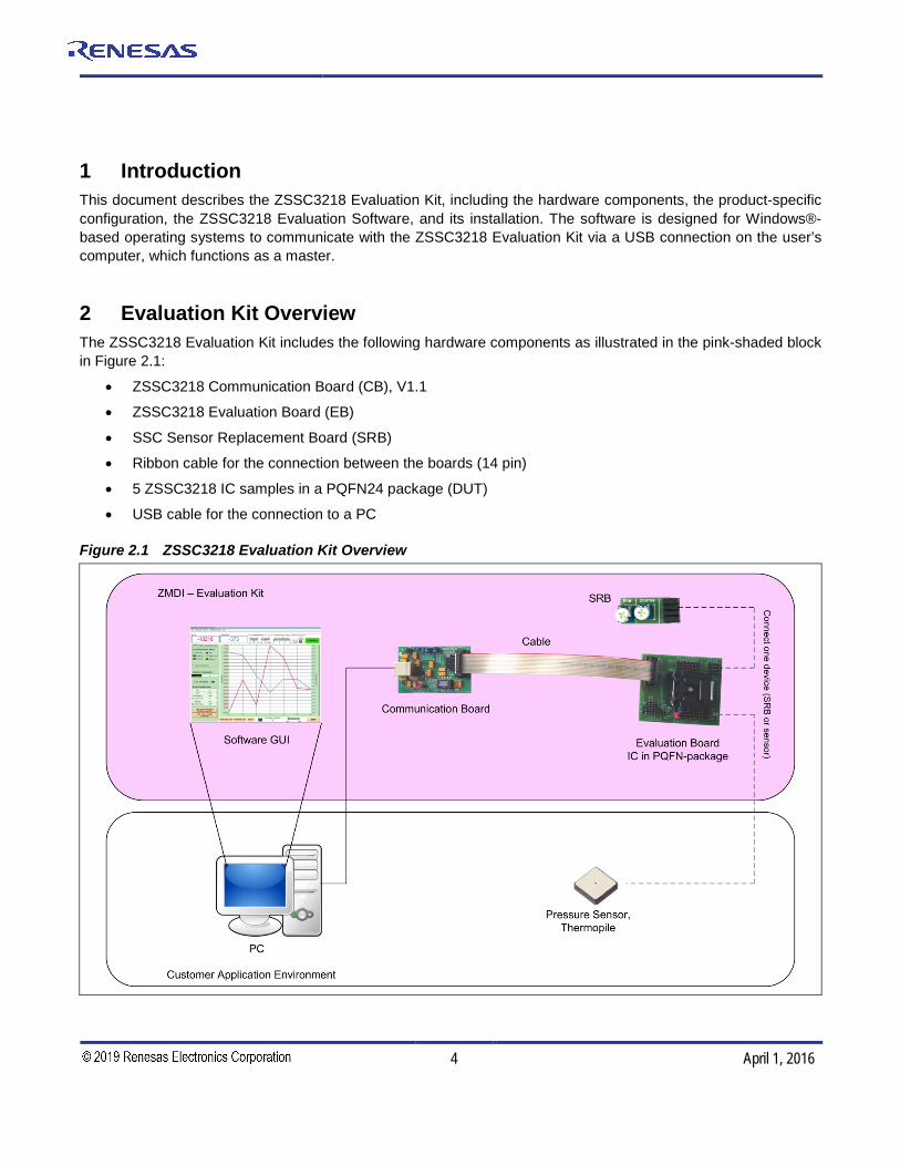
2 Evaluation Kit Overview The ZSSC3218 Evaluation Kit includes the following hardware components as illustrated in the pink-shaded block in Figure 2.1:
• ZSSC3218 Communication Board (CB), V1.1
• ZSSC3218 Evaluation Board (EB)
• SSC Sensor Replacement Board (SRB)
• Ribbon cable for the connection between the boards (14 pin)
• 5 ZSSC3218 IC samples in a PQFN24 package (DUT)
• USB cable for the connection to a PC
Figure 2.1 ZSSC3218 Evaluation Kit Overview

ZSSC3218 Evaluation Kit Description
© 2016 Integrated Device Technology, Inc. 5 April 1, 2016
To ensure that users have the most current software revision, the ZSSC3218 Evaluation Software and the documentation are available for download from www.IDT.com/ZSSC3218KIT.
The Evaluation Board provides a connection for a sensor replacement device (e.g., the SRB) or a user sensor module and an alternative 4-pad solder connection for a soldering a sensor on the Evaluation Board. Note: Only one connection can be used at a time.
Schematics for the Communication Board are provided in Appendix A. Schematics for the Evaluation Board are in Appendix B.
2.1. Installing the Software The ZSSC3218 Evaluation Kit uses an FDTI controller on the Communication Board to handle the USB protocol, translate communications, and synchronize communications with the I2C™* and/or SPI interface.
2.1.1. Installing the USB Drivers Before installing the ZSSC3218 Evaluation Software, the USB drivers for the FTDI device must be installed. Download the drivers and corresponding installation guides from www.ftdichip.com/Drivers/D2XX.htm. The Evaluation Software accesses the FTDI controller through the D2XX DLL. The drivers will not affect the operation of any other USB peripherals. For installation of the drivers, the user’s system must meet these requirements:
• x86-compatible PC• 64 MB RAM• Hard drive with 20MB free space• USB port• Windows® 2000/XP/Vista/Windows® 7/Windows® 8
Refer to http://www.ftdichip.com/Support/Documents/InstallGuides.htm (see section 6) for instructions on installing the correct driver.
2.1.2. Installing ZSSC3218 Evaluation Software Follow these instructions to install the ZSSC3218 Evaluation Software on the user’s PC hard drive. After unzipping the downloaded ZSSC3218 Evaluation Software zip file, navigate to the directory ZSSC3218 EV SW_vXpxx. (Note: Xpxx refers to the latest version number.) Double click on the setup.exe file, and follow the resulting standard installation instructions, entering installation paths and identification as needed. If the default settings have been used, the software automatically completes the installation and creates an access link under Start > All Programs > ZMDI > ZSSC3218 Evaluation.
* I2C™ is a trademark of NXP.
ZSSC3218 Evaluation Kit Description
© 2016 Integrated Device Technology, Inc. 6 April 1, 2016
3 Evaluation Kit Hardware The kit hardware consists primarily of two circuit boards: the ZSSC3218 Communication Board and the ZSSC3218 Evaluation Board. They are connected via the 14-pin ribbon cable. The Communication Board has a USB interface for the connection to the user’s computer. The Evaluation Board has a PQFN24 socket where the sample IC (a.k.a. the DUT) must be inserted.
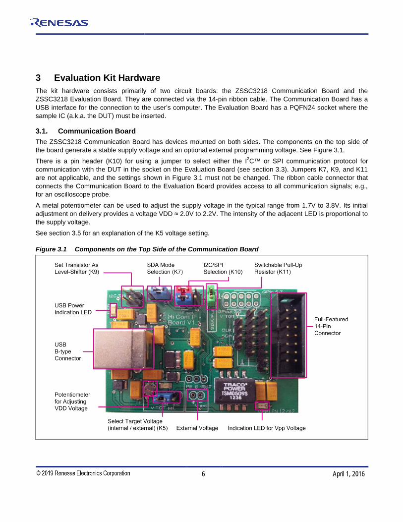
3.1. Communication Board The ZSSC3218 Communication Board has devices mounted on both sides. The components on the top side of the board generate a stable supply voltage and an optional external programming voltage. See Figure 3.1.
There is a pin header (K10) for using a jumper to select either the I2C™ or SPI communication protocol for communication with the DUT in the socket on the Evaluation Board (see section 3.3). Jumpers K7, K9, and K11 are not applicable, and the settings shown in Figure 3.1 must not be changed. The ribbon cable connector that connects the Communication Board to the Evaluation Board provides access to all communication signals; e.g., for an oscilloscope probe.
A metal potentiometer can be used to adjust the supply voltage in the typical range from 1.7V to 3.8V. Its initial adjustment on delivery provides a voltage VDD ≈ 2.0V to 2.2V. The intensity of the adjacent LED is proportional to the supply voltage.
See section 3.5 for an explanation of the K5 voltage setting.
Figure 3.1 Components on the Top Side of the Communication Board
ZSSC3218 Evaluation Kit Description
© 2016 Integrated Device Technology, Inc. 7 April 1, 2016
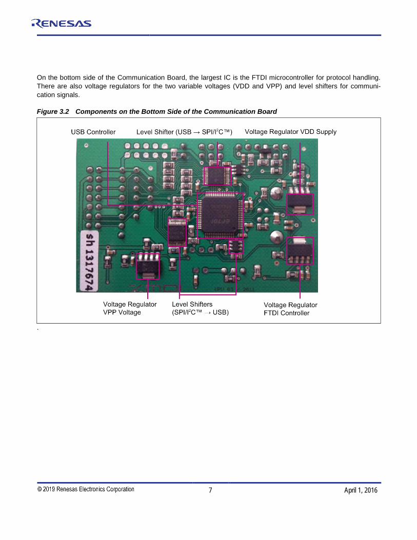
On the bottom side of the Communication Board, the largest IC is the FTDI microcontroller for protocol handling. There are also voltage regulators for the two variable voltages (VDD and VPP) and level shifters for communi-cation signals.
Figure 3.2 Components on the Bottom Side of the Communication Board
.
ZSSC3218 Evaluation Kit Description
© 2016 Integrated Device Technology, Inc. 8 April 1, 2016
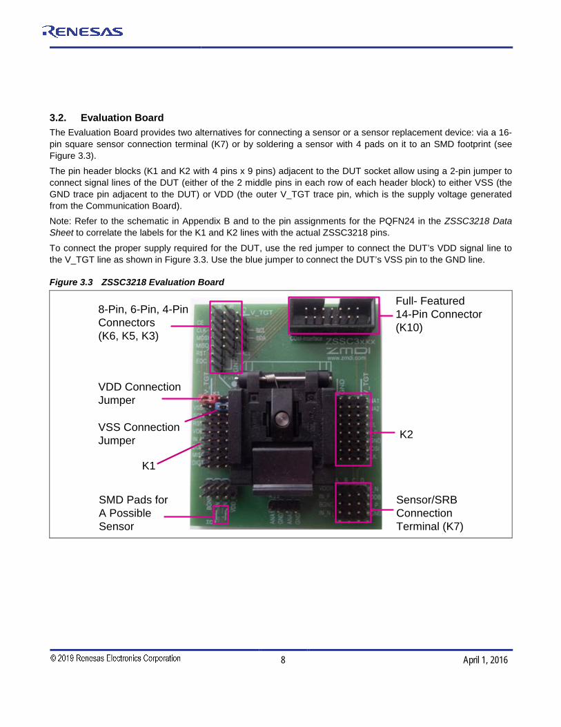
3.2. Evaluation Board The Evaluation Board provides two alternatives for connecting a sensor or a sensor replacement device: via a 16-pin square sensor connection terminal (K7) or by soldering a sensor with 4 pads on it to an SMD footprint (see Figure 3.3).
The pin header blocks (K1 and K2 with 4 pins x 9 pins) adjacent to the DUT socket allow using a 2-pin jumper to connect signal lines of the DUT (either of the 2 middle pins in each row of each header block) to either VSS (the GND trace pin adjacent to the DUT) or VDD (the outer V_TGT trace pin, which is the supply voltage generated from the Communication Board). Note: Refer to the schematic in Appendix B and to the pin assignments for the PQFN24 in the ZSSC3218 Data Sheet to correlate the labels for the K1 and K2 lines with the actual ZSSC3218 pins.
To connect the proper supply required for the DUT, use the red jumper to connect the DUT’s VDD signal line to the V_TGT line as shown in Figure 3.3. Use the blue jumper to connect the DUT’s VSS pin to the GND line.
Figure 3.3 ZSSC3218 Evaluation Board
8-Pin, 6-Pin, 4-PinConnectors(K6, K5, K3)
Full- Featured 14-Pin Connector(K10)
VDD Connection Jumper
VSS Connection Jumper
SMD Pads for A Possible Sensor
Sensor/SRB Connection Terminal (K7)
K2
K1
ZSSC3218 Evaluation Kit Description
© 2016 Integrated Device Technology, Inc. 9 April 1, 2016
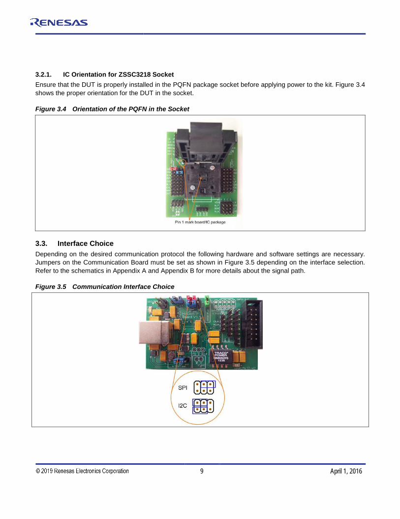
3.2.1. IC Orientation for ZSSC3218 Socket Ensure that the DUT is properly installed in the PQFN package socket before applying power to the kit. Figure 3.4 shows the proper orientation for the DUT in the socket.
Figure 3.4 Orientation of the PQFN in the Socket
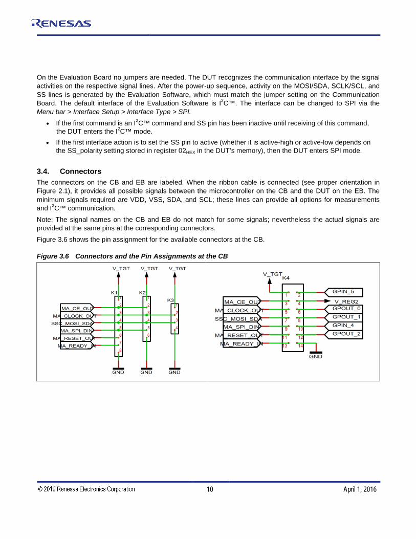
3.3. Interface Choice Depending on the desired communication protocol the following hardware and software settings are necessary. Jumpers on the Communication Board must be set as shown in Figure 3.5 depending on the interface selection. Refer to the schematics in Appendix A and Appendix B for more details about the signal path.
Figure 3.5 Communication Interface Choice
ZSSC3218 Evaluation Kit Description
© 2016 Integrated Device Technology, Inc. 10 April 1, 2016
On the Evaluation Board no jumpers are needed. The DUT recognizes the communication interface by the signal activities on the respective signal lines. After the power-up sequence, activity on the MOSI/SDA, SCLK/SCL, and SS lines is generated by the Evaluation Software, which must match the jumper setting on the Communication Board. The default interface of the Evaluation Software is I2C™. The interface can be changed to SPI via the Menu bar > Interface Setup > Interface Type > SPI.
• If the first command is an I2C™ command and SS pin has been inactive until receiving of this command,the DUT enters the I2C™ mode.
• If the first interface action is to set the SS pin to active (whether it is active-high or active-low depends onthe SS_polarity setting stored in register 02HEX in the DUT’s memory), then the DUT enters SPI mode.
3.4. Connectors The connectors on the CB and EB are labeled. When the ribbon cable is connected (see proper orientation in Figure 2.1), it provides all possible signals between the microcontroller on the CB and the DUT on the EB. The minimum signals required are VDD, VSS, SDA, and SCL; these lines can provide all options for measurements and I2C™ communication.
Note: The signal names on the CB and EB do not match for some signals; nevertheless the actual signals are provided at the same pins at the corresponding connectors.
Figure 3.6 shows the pin assignment for the available connectors at the CB.
Figure 3.6 Connectors and the Pin Assignments at the CB
ZSSC3218 Evaluation Kit Description
© 2016 Integrated Device Technology, Inc. 11 April 1, 2016
Figure 3.7 Connectors and the Pin Assignments at EB
3.5. Supply Voltage The Evaluation Kit can be powered with an internal or external voltage supply for the DUT on the Evaluation Board, which must be selected with the jumper on the K5 pin header on the CB (see Figure 3.8). There are no settings for selecting the supply source on the EB.
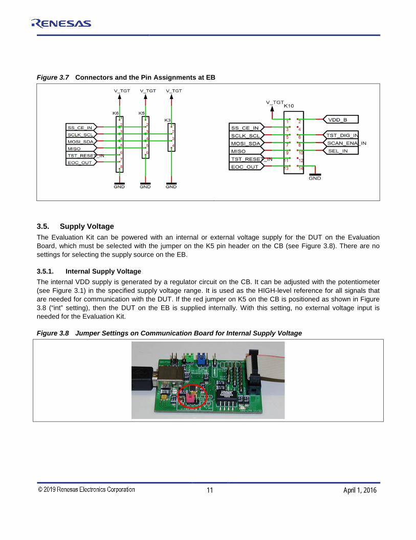
3.5.1. Internal Supply Voltage The internal VDD supply is generated by a regulator circuit on the CB. It can be adjusted with the potentiometer (see Figure 3.1) in the specified supply voltage range. It is used as the HIGH-level reference for all signals that are needed for communication with the DUT. If the red jumper on K5 on the CB is positioned as shown in Figure 3.8 (“int” setting), then the DUT on the EB is supplied internally. With this setting, no external voltage input is needed for the Evaluation Kit.
Figure 3.8 Jumper Settings on Communication Board for Internal Supply Voltage

ZSSC3218 Evaluation Kit Description
© 2016 Integrated Device Technology, Inc. 12 April 1, 2016
3.5.2. External Supply Voltage An alternative for providing the supply voltage to the DUT is to input an external voltage supply source. Ensure that the external voltage does not exceed the voltage supply specifications given in the IDT data sheet for the DUT before connecting to the Evaluation Kit.
To use an external supply, set the K5 jumper as shown in Figure 3.9 (“ext” setting). Connect the external voltage to the 2-pin V_ext header that is immediately to the right of the K5 jumper with the orientation shown in Figure 3.9. There are no adjustments for the external voltage on either the CB or EB.
Figure 3.9 Jumper Settings on the Communication Board for the External Supply Voltage
ZSSC3218 Evaluation Kit Description
© 2016 Integrated Device Technology, Inc. 13 April 1, 2016
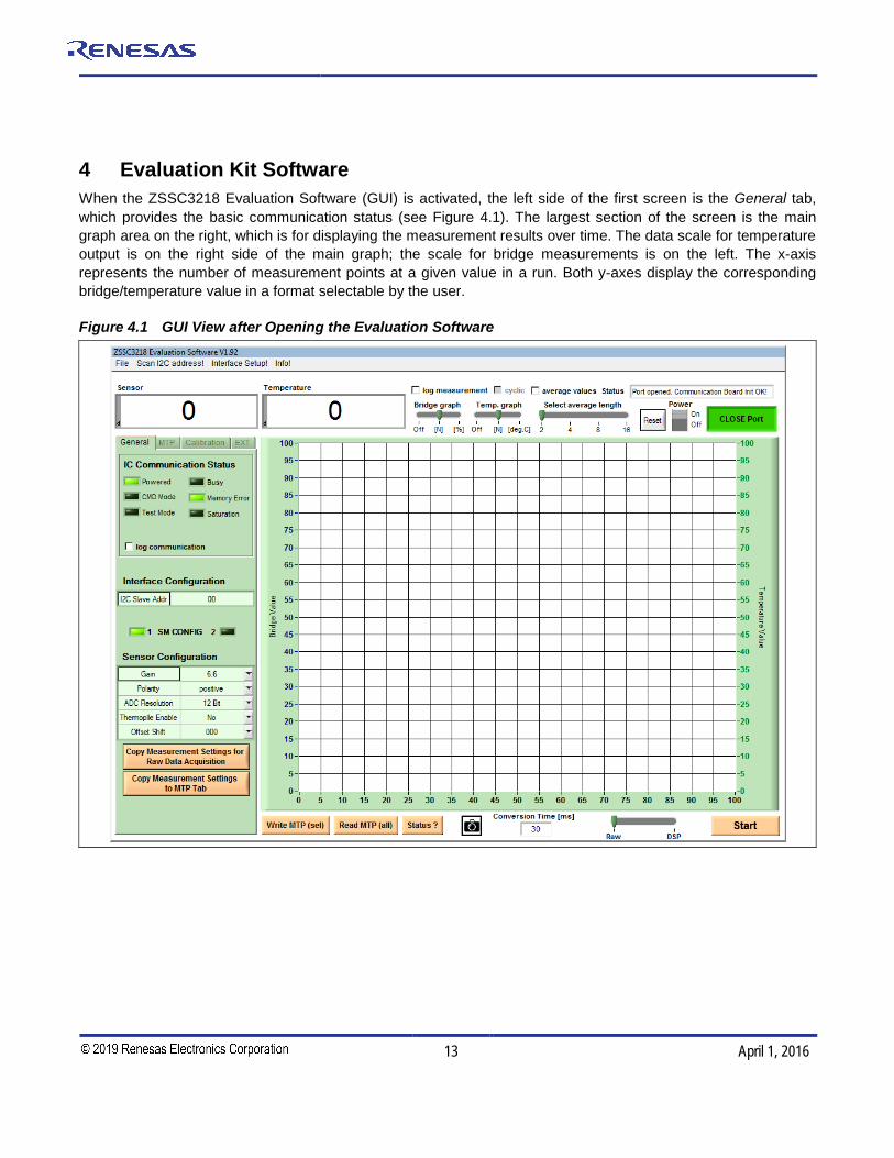
4 Evaluation Kit Software When the ZSSC3218 Evaluation Software (GUI) is activated, the left side of the first screen is the General tab, which provides the basic communication status (see Figure 4.1). The largest section of the screen is the main graph area on the right, which is for displaying the measurement results over time. The data scale for temperature output is on the right side of the main graph; the scale for bridge measurements is on the left. The x-axis represents the number of measurement points at a given value in a run. Both y-axes display the corresponding bridge/temperature value in a format selectable by the user.
Figure 4.1 GUI View after Opening the Evaluation Software
ZSSC3218 Evaluation Kit Description
© 2016 Integrated Device Technology, Inc. 14 April 1, 2016
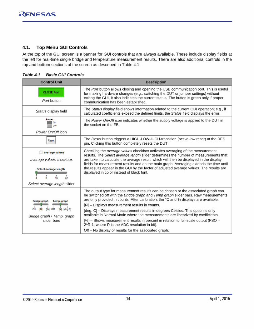
4.1. Top Menu GUI Controls At the top of the GUI screen is a banner for GUI controls that are always available. These include display fields at the left for real-time single bridge and temperature measurement results. There are also additional controls in the top and bottom sections of the screen as described in Table 4.1.
Table 4.1 Basic GUI Controls Control Unit Description
Port button
The Port button allows closing and opening the USB communication port. This is useful for making hardware changes (e.g., switching the DUT or jumper settings) without exiting the GUI. It also indicates the current status. The button is green only if proper communication has been established.
Status display field The Status display field shows information related to the current GUI operation; e.g., if calculated coefficients exceed the defined limits, the Status field displays the error.
Power On/Off icon
The Power On/Off icon indicates whether the supply voltage is applied to the DUT in the socket on the EB.
The Reset button triggers a HIGH-LOW-HIGH-transition (active-low reset) at the RES pin. Clicking this button completely resets the DUT.
average values checkbox
Select average length slider
Checking the average values checkbox activates averaging of the measurement results. The Select average length slider determines the number of measurements that are taken to calculate the average result, which will then be displayed in the display fields for measurement results and on the main graph. Averaging extends the time until the results appear in the GUI by the factor of adjusted average values. The results are displayed in color instead of black font.
Bridge graph / Temp. graph slider bars
The output type for measurement results can be chosen or the associated graph can be switched off with the Bridge graph and Temp graph slider bars. Raw measurements are only provided in counts. After calibration, the °C and % displays are available. [N] – Displays measurement results in counts.[deg. C] – Displays measurement results in degrees Celsius. This option is only available in Normal Mode where the measurements are linearized by coefficients. [%] – Shows measurement results in percent in relation to full-scale output (FSO = 2^R-1, where R is the ADC resolution in bit). Off – No display of results for the associated graph.
ZSSC3218 Evaluation Kit Description
© 2016 Integrated Device Technology, Inc. 15 April 1, 2016
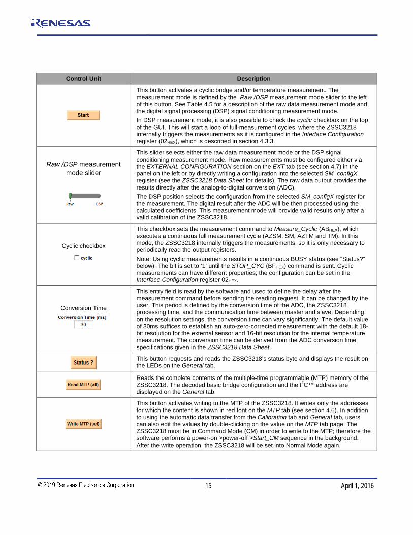
Control Unit Description
This button activates a cyclic bridge and/or temperature measurement. The measurement mode is defined by the Raw /DSP measurement mode slider to the left of this button. See Table 4.5 for a description of the raw data measurement mode and the digital signal processing (DSP) signal conditioning measurement mode. In DSP measurement mode, it is also possible to check the cyclic checkbox on the top of the GUI. This will start a loop of full-measurement cycles, where the ZSSC3218 internally triggers the measurements as it is configured in the Interface Configuration register (02HEX), which is described in section 4.3.3.
Raw /DSP measurement mode slider
This slider selects either the raw data measurement mode or the DSP signal conditioning measurement mode. Raw measurements must be configured either via the EXTERNAL CONFIGURATION section on the EXT tab (see section 4.7) in the panel on the left or by directly writing a configuration into the selected SM_configX register (see the ZSSC3218 Data Sheet for details). The raw data output provides the results directly after the analog-to-digital conversion (ADC). The DSP position selects the configuration from the selected SM_configX register for the measurement. The digital result after the ADC will be then processed using the calculated coefficients. This measurement mode will provide valid results only after a valid calibration of the ZSSC3218.
Cyclic checkbox
This checkbox sets the measurement command to Measure_Cyclic (ABHEX), which executes a continuous full measurement cycle (AZSM, SM, AZTM and TM). In this mode, the ZSSC3218 internally triggers the measurements, so it is only necessary to periodically read the output registers. Note: Using cyclic measurements results in a continuous BUSY status (see “Status?” below). The bit is set to ‘1’ until the STOP_CYC (BFHEX) command is sent. Cyclic measurements can have different properties; the configuration can be set in the Interface Configuration register 02HEX.
Conversion Time
This entry field is read by the software and used to define the delay after the measurement command before sending the reading request. It can be changed by the user. This period is defined by the conversion time of the ADC, the ZSSC3218 processing time, and the communication time between master and slave. Depending on the resolution settings, the conversion time can vary significantly. The default value of 30ms suffices to establish an auto-zero-corrected measurement with the default 18-bit resolution for the external sensor and 16-bit resolution for the internal temperature measurement. The conversion time can be derived from the ADC conversion time specifications given in the ZSSC3218 Data Sheet.
This button requests and reads the ZSSC3218’s status byte and displays the result on the LEDs on the General tab.
Reads the complete contents of the multiple-time programmable (MTP) memory of the ZSSC3218. The decoded basic bridge configuration and the I2C™ address are displayed on the General tab.
This button activates writing to the MTP of the ZSSC3218. It writes only the addresses for which the content is shown in red font on the MTP tab (see section 4.6). In addition to using the automatic data transfer from the Calibration tab and General tab, users can also edit the values by double-clicking on the value on the MTP tab page. The ZSSC3218 must be in Command Mode (CM) in order to write to the MTP; therefore the software performs a power-on >power-off >Start_CM sequence in the background. After the write operation, the ZSSC3218 will be set into Normal Mode again.
ZSSC3218 Evaluation Kit Description
© 2016 Integrated Device Technology, Inc. 16 April 1, 2016
4.2. Measurement Color Code Bridge and temperature results are displayed in different colors. Different colors are also used for single and averaged measurement results as defined in Table 4.2
Table 4.2 Color Code for Bridge and Temperature Results Color Indication
Pink Single bridge measurement.
Light Blue Single temperature measurement.
Blue Averaged bridge measurement.
Green Averaged temperature measurement.
Red Invalid measurement result. This could be due to a Conversion Time that is too short. In this case, bit 5 in the status byte is set to ‘1’ and the Busy virtual LED on the General tab turns on. Another reason for an invalid measurement result could be if saturation of the arithmetic logic unit (ALU) is detected. In this case, the Saturation LED turns on.
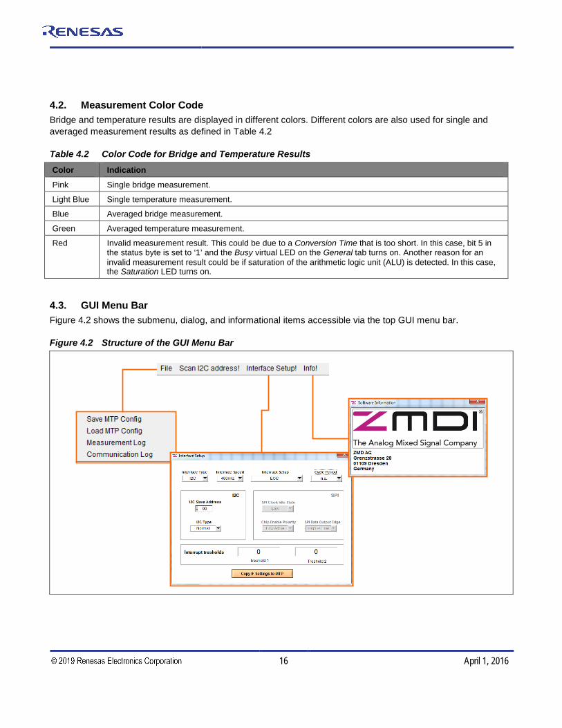
4.3. GUI Menu Bar Figure 4.2 shows the submenu, dialog, and informational items accessible via the top GUI menu bar.
Figure 4.2 Structure of the GUI Menu Bar

ZSSC3218 Evaluation Kit Description
© 2016 Integrated Device Technology, Inc. 17 April 1, 2016
4.3.1. Save/Load MTP Register Contents Initially, the customer memory pages are empty. If an identical memory configuration is needed for multiple ICs, it is possible to save a given setup as a template. When the required MTP content is present in the MTP tab, select File > Save MTP Config. The configuration file is created with an .eep extension, and it contains one decimal value for each MTP address in each row. To load a configuration file, select File > Load MTP Config. Note: The decimal values will be automatically dis-played as hexadecimal values in the MTP tab. The loaded configuration data is displayed in red font in the MTP tab and can be written into the memory.
4.3.2. Scan I2C™ Bus via the Scan I2C address! Feature Another feature provided in the menu bar is the ability to scan the I2C™ bus to determine the I2C™ address of the ZSSC3218. Selecting Scan I2C address triggers the scan during which the ZSSC3218 status is requested for each address ranging from 00HEX to 7FHEX. When an I2C™ address is acknowledged by the ZSSC3218, the scan stops, and this address is used for further communication during the current GUI session. The results of the scan are indicated in the status window:
• Status window message for a successful I2C™ scan: Valid I2C address found: 0xXX!• Status window message for an I2C™ scan without slave acknowledge: No valid I2C address found!
The I2C™ address information is lost if the GUI or the communication port is closed. Communication to the ZSSC3218 with an I2C™ address other than 00HEX can also be established by entering it manually in the Interface Setup dialog accessible via the top menu bar by selecting Interface Setup and entering the hexadecimal address in the I2C Slave Address field.
4.3.3. Interface Setup Dialog The interface setup dialog allows the general choice between the I2C™ and the SPI interface. After an interface is selected, the software generates the corresponding data frame structure which is then recognized by the ZSSC3218. All parameters in the upper row (Interface Type, Interface Speed, Interrupt Setup, and Cycle Period) and the I2C/SPI specific settings in the corresponding section are parameters from the Interface Configuration register (02HEX). The lower part of the window displays the selectable lower and upper threshold values for the interrupt configuration (see ZSSC3218 Data Sheet for details). Enter the values in the decimal representation.
Modifications entered in the dialog are valid for further communication after this window is closed. To save the changes in the ZSSC3218’s memory, adjust the parameters as needed and click the Copy IF settings to memory button to transfer it to the MTP tab in the GUI. As a result, the registers 02HEX (Interface Configuration) and/or registers 13HEX, 14HEX, and 15HEX (interrupt thresholds) appear red if their content changed. Then click the Write MTP (sel) button on the MTP tab to write the new content into the memory.
ZSSC3218 Evaluation Kit Description
© 2016 Integrated Device Technology, Inc. 18 April 1, 2016
4.4. GUI – General Tab
Table 4.3 General Tab –Displays and Controls Control / Display Unit Description
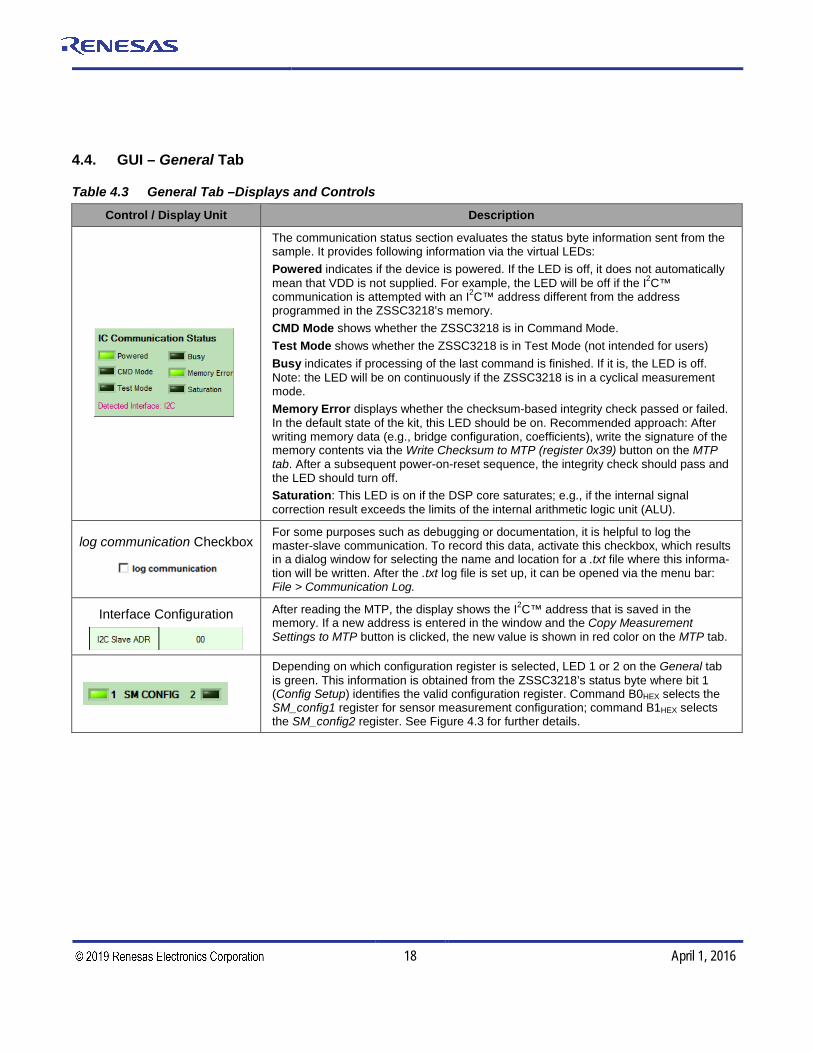
The communication status section evaluates the status byte information sent from the sample. It provides following information via the virtual LEDs: Powered indicates if the device is powered. If the LED is off, it does not automatically mean that VDD is not supplied. For example, the LED will be off if the I2C™ communication is attempted with an I2C™ address different from the address programmed in the ZSSC3218’s memory. CMD Mode shows whether the ZSSC3218 is in Command Mode. Test Mode shows whether the ZSSC3218 is in Test Mode (not intended for users) Busy indicates if processing of the last command is finished. If it is, the LED is off. Note: the LED will be on continuously if the ZSSC3218 is in a cyclical measurement mode. Memory Error displays whether the checksum-based integrity check passed or failed. In the default state of the kit, this LED should be on. Recommended approach: After writing memory data (e.g., bridge configuration, coefficients), write the signature of the memory contents via the Write Checksum to MTP (register 0x39) button on the MTP tab. After a subsequent power-on-reset sequence, the integrity check should pass and the LED should turn off. Saturation: This LED is on if the DSP core saturates; e.g., if the internal signal correction result exceeds the limits of the internal arithmetic logic unit (ALU).
log communication Checkbox For some purposes such as debugging or documentation, it is helpful to log the master-slave communication. To record this data, activate this checkbox, which results in a dialog window for selecting the name and location for a .txt file where this informa-tion will be written. After the .txt log file is set up, it can be opened via the menu bar: File > Communication Log.
Interface Configuration After reading the MTP, the display shows the I2C™ address that is saved in the memory. If a new address is entered in the window and the Copy Measurement Settings to MTP button is clicked, the new value is shown in red color on the MTP tab.
Depending on which configuration register is selected, LED 1 or 2 on the General tab is green. This information is obtained from the ZSSC3218’s status byte where bit 1 (Config Setup) identifies the valid configuration register. Command B0HEX selects the SM_config1 register for sensor measurement configuration; command B1HEX selects the SM_config2 register. See Figure 4.3 for further details.
ZSSC3218 Evaluation Kit Description
© 2016 Integrated Device Technology, Inc. 19 April 1, 2016
Control / Display Unit Description
Sensor Configuration The Sensor Configuration area provides settings for the analog signal path and analog-to-digital conversion. The drop-down menus contain the available setting values. Changing the parameter values here does not automatically apply them to measure-ments. It is possible to apply the adjusted settings and use them for raw data collection. There are different commands for performing raw measurements. Some of the commands use the configuration from the SM_config register (commands A0HEX, A2HEX); others (A1HEX, A3HEX) are configured via the interface. For a full description of raw measurement commands, refer to section 4.7.1. For configuration via the interface, click on the Copy Measurement Settings for Raw Data Acquisition button, which automatically displays the EXT tab (see section 4.7) and transfers the present settings to the external configuration section. The Copy Measurement Settings to MTP Tab button copies the present settings to the MTP tab. The settings can then be written to the MTP memory (see section 4.6).
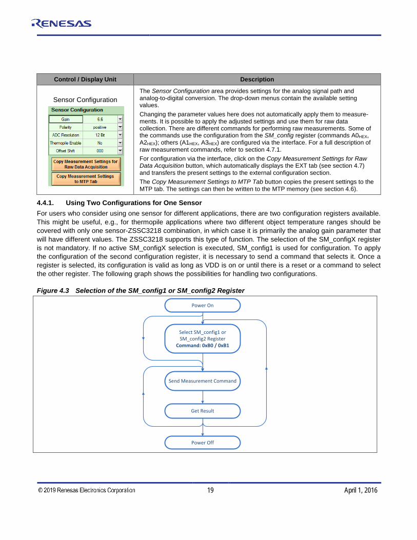
4.4.1. Using Two Configurations for One Sensor For users who consider using one sensor for different applications, there are two configuration registers available. This might be useful, e.g., for thermopile applications where two different object temperature ranges should be covered with only one sensor-ZSSC3218 combination, in which case it is primarily the analog gain parameter that will have different values. The ZSSC3218 supports this type of function. The selection of the SM_configX register is not mandatory. If no active SM_configX selection is executed, SM_config1 is used for configuration. To apply the configuration of the second configuration register, it is necessary to send a command that selects it. Once a register is selected, its configuration is valid as long as VDD is on or until there is a reset or a command to select the other register. The following graph shows the possibilities for handling two configurations.
Figure 4.3 Selection of the SM_config1 or SM_config2 Register
Select SM_config1 or SM_config2 Register
Command: 0xB0 / 0xB1
Send Measurement Command
Get Result
Power On
Power Off
ZSSC3218 Evaluation Kit Description
© 2016 Integrated Device Technology, Inc. 20 April 1, 2016
4.5. Data Logging The ZSSC3218 Evaluation Kit software provides the option to log measurement and communication data as described in Table 4.1 and Table 4.3.
4.5.1. Communication Log Communication with the ZSSC3218 can be logged for both the I2C™ and SPI interface. Click on the log communication checkbox on the General tab to activate recording the data stream. Choose a file path for which the user has writing permission for storing the log file. Open the log file via the top menu bar: File > Communication Log. The resulting text file is an ASCII file that can be imported into Microsoft® Excel.
4.5.1.1. I2C™ Log
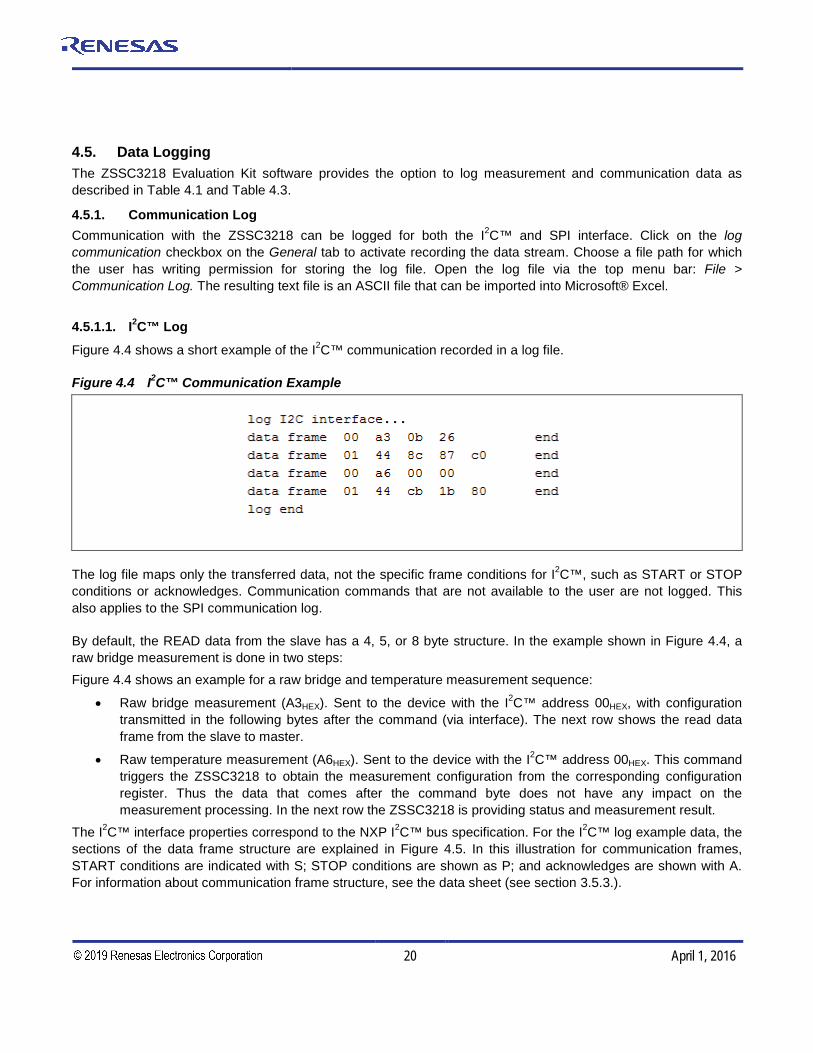
Figure 4.4 shows a short example of the I2C™ communication recorded in a log file.
Figure 4.4 I2C™ Communication Example
The log file maps only the transferred data, not the specific frame conditions for I2C™, such as START or STOP conditions or acknowledges. Communication commands that are not available to the user are not logged. This also applies to the SPI communication log.
By default, the READ data from the slave has a 4, 5, or 8 byte structure. In the example shown in Figure 4.4, a raw bridge measurement is done in two steps: Figure 4.4 shows an example for a raw bridge and temperature measurement sequence:
• Raw bridge measurement (A3HEX). Sent to the device with the I2C™ address 00HEX, with configurationtransmitted in the following bytes after the command (via interface). The next row shows the read dataframe from the slave to master.
• Raw temperature measurement (A6HEX). Sent to the device with the I2C™ address 00HEX. This commandtriggers the ZSSC3218 to obtain the measurement configuration from the corresponding configurationregister. Thus the data that comes after the command byte does not have any impact on themeasurement processing. In the next row the ZSSC3218 is providing status and measurement result.
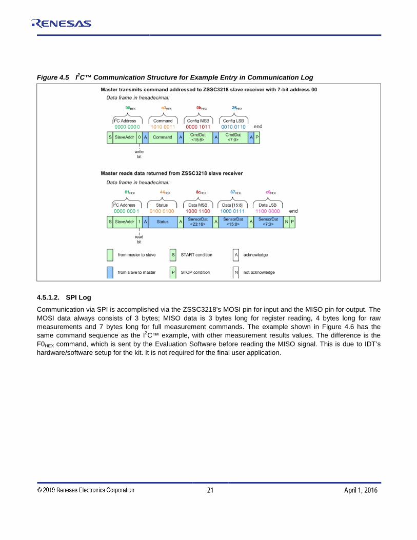
The I2C™ interface properties correspond to the NXP I2C™ bus specification. For the I2C™ log example data, the sections of the data frame structure are explained in Figure 4.5. In this illustration for communication frames, START conditions are indicated with S; STOP conditions are shown as P; and acknowledges are shown with A. For information about communication frame structure, see the data sheet (see section 3.5.3.).
ZSSC3218 Evaluation Kit Description
© 2016 Integrated Device Technology, Inc. 21 April 1, 2016
Figure 4.5 I2C™ Communication Structure for Example Entry in Communication Log
4.5.1.2. SPI Log
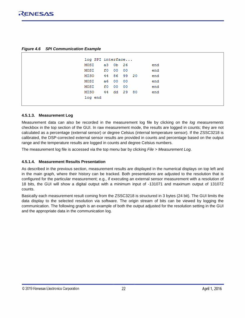
Communication via SPI is accomplished via the ZSSC3218’s MOSI pin for input and the MISO pin for output. The MOSI data always consists of 3 bytes; MISO data is 3 bytes long for register reading, 4 bytes long for raw measurements and 7 bytes long for full measurement commands. The example shown in Figure 4.6 has the same command sequence as the I2C™ example, with other measurement results values. The difference is the F0HEX command, which is sent by the Evaluation Software before reading the MISO signal. This is due to IDT’s hardware/software setup for the kit. It is not required for the final user application.
ZSSC3218 Evaluation Kit Description
© 2016 Integrated Device Technology, Inc. 22 April 1, 2016
Figure 4.6 SPI Communication Example
4.5.1.3. Measurement Log
Measurement data can also be recorded in the measurement log file by clicking on the log measurements checkbox in the top section of the GUI. In raw measurement mode, the results are logged in counts; they are not calculated as a percentage (external sensor) or degree Celsius (internal temperature sensor). If the ZSSC3218 is calibrated, the DSP-corrected external sensor results are provided in counts and percentage based on the output range and the temperature results are logged in counts and degree Celsius numbers. The measurement log file is accessed via the top menu bar by clicking File > Measurement Log.
4.5.1.4. Measurement Results Presentation
As described in the previous section, measurement results are displayed in the numerical displays on top left and in the main graph, where their history can be tracked. Both presentations are adjusted to the resolution that is configured for the particular measurement; e.g., if executing an external sensor measurement with a resolution of 18 bits, the GUI will show a digital output with a minimum input of -131071 and maximum output of 131072 counts.
Basically each measurement result coming from the ZSSC3218 is structured in 3 bytes (24 bit). The GUI limits the data display to the selected resolution via software. The origin stream of bits can be viewed by logging the communication. The following graph is an example of both the output adjusted for the resolution setting in the GUI and the appropriate data in the communication log.
ZSSC3218 Evaluation Kit Description
© 2016 Integrated Device Technology, Inc. 23 April 1, 2016
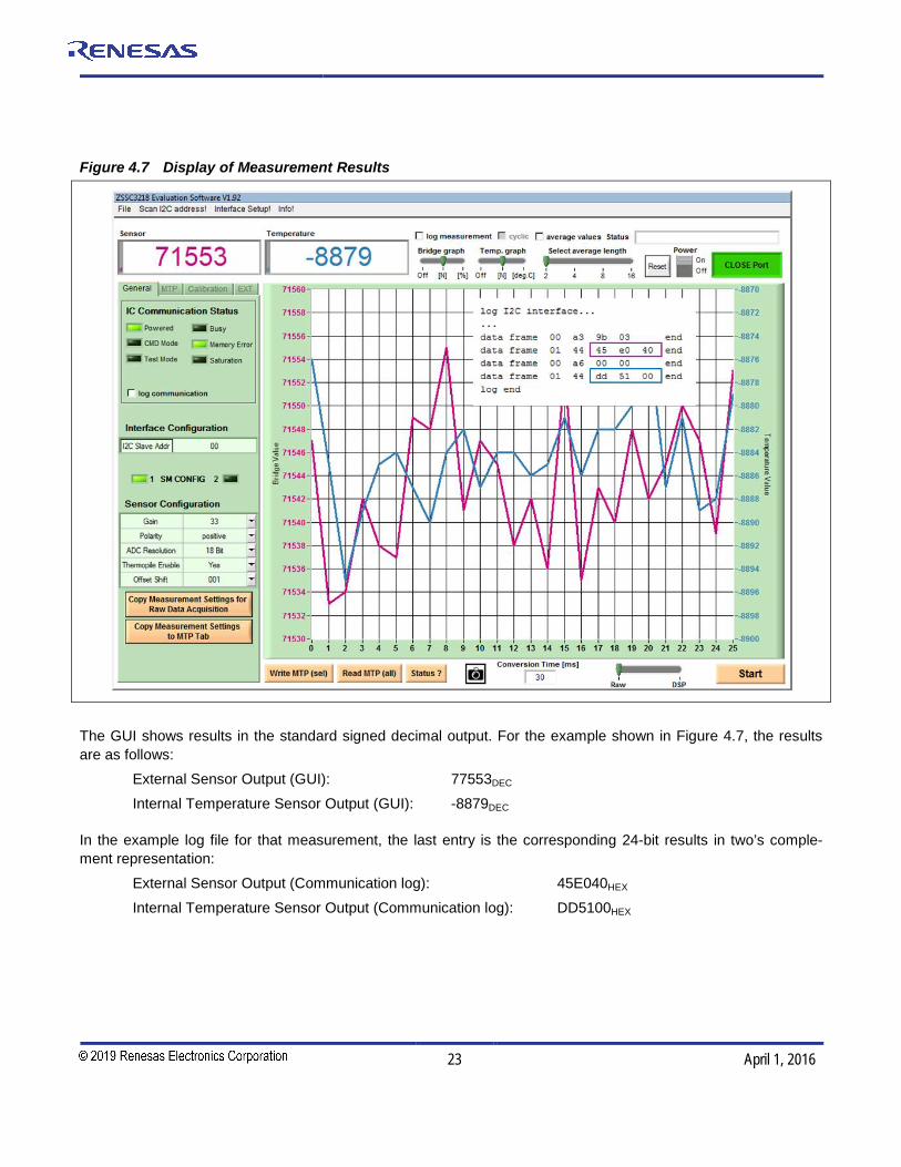
Figure 4.7 Display of Measurement Results
The GUI shows results in the standard signed decimal output. For the example shown in Figure 4.7, the results are as follows:
External Sensor Output (GUI): 77553DEC
Internal Temperature Sensor Output (GUI): -8879DEC
In the example log file for that measurement, the last entry is the corresponding 24-bit results in two’s comple-ment representation:
External Sensor Output (Communication log): 45E040HEX
Internal Temperature Sensor Output (Communication log): DD5100HEX
ZSSC3218 Evaluation Kit Description
© 2016 Integrated Device Technology, Inc. 24 April 1, 2016
In the example shown in Figure 4.7, the selected resolution for both the sensor and temperature measurements is 16 bit. The conversion from the 24-bit two’s complement value to the decimal presentation is shown in the following table.
Table 4.4 Measurement Results Conversion (24-bit two’s complement to decimal)
Operation Sensor Temperature Notes
45E040 DD5100 24-bit two's complement, hexadecimal
>> 6 Shift the external sensor value by 6 bits to the right (convert 24 bits >> 18 bits)
>> 8 Shift the temperature value by 8 bits to the right (convert 24 bits >> 16 bits)
= 11781 18-bit two's complement, hexadecimal
= DD51 16-bit two's complement, hexadecimal
dec 71553 -8879 Convert to decimal
The results correspond to the GUI display in Figure 4.7.
ZSSC3218 Evaluation Kit Description
© 2016 Integrated Device Technology, Inc. 25 April 1, 2016
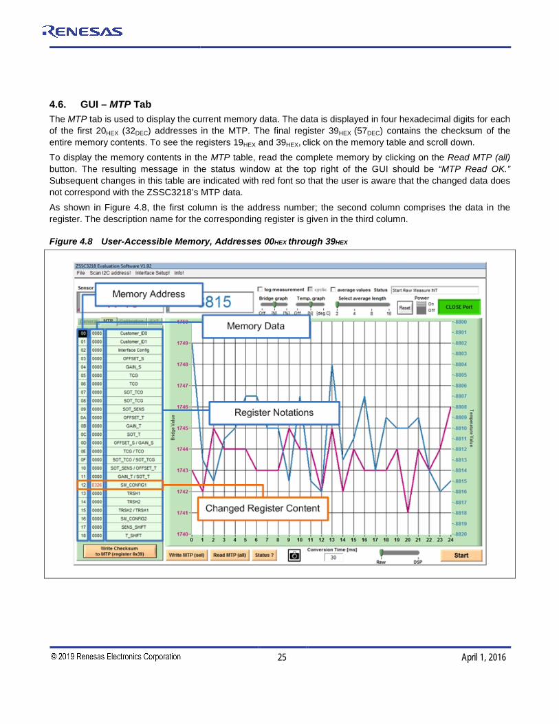
4.6. GUI – MTP Tab The MTP tab is used to display the current memory data. The data is displayed in four hexadecimal digits for each of the first 20HEX (32DEC) addresses in the MTP. The final register 39HEX (57DEC) contains the checksum of the entire memory contents. To see the registers 19HEX and 39HEX, click on the memory table and scroll down. To display the memory contents in the MTP table, read the complete memory by clicking on the Read MTP (all) button. The resulting message in the status window at the top right of the GUI should be “MTP Read OK.” Subsequent changes in this table are indicated with red font so that the user is aware that the changed data does not correspond with the ZSSC3218’s MTP data. As shown in Figure 4.8, the first column is the address number; the second column comprises the data in the register. The description name for the corresponding register is given in the third column.
Figure 4.8 User-Accessible Memory, Addresses 00HEX through 39HEX
ZSSC3218 Evaluation Kit Description
© 2016 Integrated Device Technology, Inc. 26 April 1, 2016
Clicking the Write Checksum to MTP (register 39HEX) button at the bottom of the MTP tab triggers the signature generation and writing the new signature over the current memory contents for register 39HEX. Therefore it should be the last step to be done after bridge measurement configuration, coefficient calculation, and writing. After the checksum has been written and the ZSSC3218 has been re-powered, the Memory Error LED turns off (see Table 4.3).
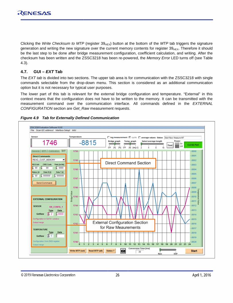
4.7. GUI – EXT Tab The EXT tab is divided into two sections. The upper tab area is for communication with the ZSSC3218 with single commands selectable from the drop-down menu. This section is considered as an additional communication option but it is not necessary for typical user purposes.
The lower part of this tab is relevant for the external bridge configuration and temperature. “External” in this context means that the configuration does not have to be written to the memory. It can be transmitted with the measurement command over the communication interface. All commands defined in the EXTERNAL CONFIGURATION section are Get_Raw measurement requests.
Figure 4.9 Tab for Externally Defined Communication

ZSSC3218 Evaluation Kit Description
© 2016 Integrated Device Technology, Inc. 27 April 1, 2016
In the “Sensor” and “Temperature” subsections of the EXTERNAL CONFIGURATION section, the Type window defines the Get_Raw command and the Data window selects the measurement configuration if required. Refer to Table 4.5 for the descriptions of the possible commands and the data. Example: In the “Bridge” section, an entry of 3HEX in the Type field and 0225HEX in the Data field corresponds to the GetRaw command A3 0225HEX.
4.7.1. Get_Raw Commands Eight Get_Raw commands for data acquisition are available, depending on the measurement type and the source of the configuration; however, there are basically only two different commands: the single measurement and the auto-zero measurement, which selects the ADC offset. These are applied to the bridge and temperature measurements with different configuration origins. All measurement command options are described in the Table 4.5.
Table 4.5 Get_Raw Commands
Command Measurement AFE Configuration Register
Type Data
A0HEX 0000HEX SM – Bridge Measurement SM_config1 register or SM_config2 register
A1HEX ssssHEX SM – Bridge Measurement ssss is the user’s configuration setting for the mea-surement provided via the interface. The format and purpose of configuration bits must be consistent with the definitions given for the SM_configX register. (See the ZSSC3218 Data Sheet.)
A2HEX 0000HEX SM-AZSM – Auto-Zero Corrected Sridge Measurement SM_config
A3HEX ssssHEX SM-AZSM – Auto-Zero Corrected Bridge Measurement
ssss is the user’s configuration setting for the mea-surement provided via the interface. The format and purpose of configuration bits must be equal to the definitions for SM_configX.
A4HEX 0000HEX TM – Temperature Measurement IDT-defined register.
A6HEX 0000HEX TM-AZTM – Auto-Zero Corrected Temperature Measurement IDT-defined register.
Raw commands with Auto-Zero correction measure the system internal offset and subtract it from the common measurement result.
4.7.2. Data Output Range Any ADC measurement and its calculated sensor signal conditioned output are formatted as a 24-bit wide data word, regardless of the effective selected ADC resolution. The Evaluation Software reduces the resolution to the resolution configured for the measurement. Table 4.6 illustrates the GUI output ranges depending on the resolu-tion and operation mode. The raw measurement output is the ADC data without passing through the DSP. The current common range is shown in the GUI in the SENSOR and TEMPERATURE section in the EXT tab. Output data in Normal Mode is digitally corrected and adjusted to the full-scale output of the valid resolution if the device has been calibrated correctly.
ZSSC3218 Evaluation Kit Description
© 2016 Integrated Device Technology, Inc. 28 April 1, 2016
Table 4.6 GUI Output Ranges
Operation Mode Numerical Format ADC Resolution (bits)
GUI Display and Measurement Log
Min Max
Raw Measurement Decimal
12 -2048(-211)
2047 (211 – 1)
13 -4096(-212)
4095 (212 – 1)
… … …
18 -131072
(-217)131071
(217 – 1)
Normal Mode Decimal
12 0 4095
(212 – 1)
13 0 8191
(213 – 1)
… … …
18 0 262143
(218 – 1)
Calibration Table (see section 4.8) Decimal 12, 13, …18
-8388608(-223)
8388607 (223 – 1)
Measurement log Decimal Same as in raw measurement
Communication log Hexadecimal Two’s Complement
Same as in calibration table
4.7.3. Setting up Bridge Configuration for Calibration If the sensor characteristics are known, the external sensor measurement settings can be defined in the General tab.
The following parameters can be configured:
• Bridge Gain: The analog gain is applied in two different amplifier stages. The possible gain factors ofthese two stages are selectable in the drop-down menu. Recommendation: Choose the bridge gain ashigh as possible in order to take full advantage of the ADC’s dynamic range.
• Bridge Polarity: The ZSSC3218 has the capability to switch the polarity of the sensor input INP and INN.This setting is only valid if the differential sensor signal has a higher negative voltage output range thanthe positive one:
if ( abs(Vmax) < abs (Vmin)) ) Bridge Polarity = 1 else Bridge Polarity = 0
ZSSC3218 Evaluation Kit Description
© 2016 Integrated Device Technology, Inc. 29 April 1, 2016
• Thermopile (AbsV) Enable: Enable bit for thermopile input selection (INN connected to AGND, INPconnected absolute voltage source)
• Bridge Offset Shift: Depending on the sensor output, the offset can be adjusted to ADC’s input by aprogrammable offset. The offset can be chosen from 8 different values. For further details, refer to theZSSC3218 Data Sheet.
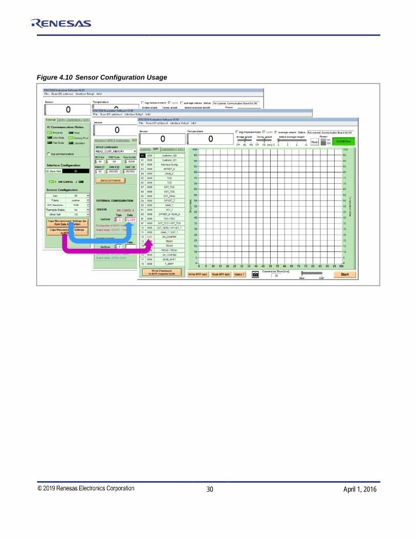
4.7.4. Starting External Sensor Measurement After determining the best fit for the external sensor measurement configuration, it can be applied. Two options are available for raw measurements of an external sensor:
Configuration, transmitted via communication interface:
Adjust settings in the Sensor Configuration section (General tab) Click the Copy Measurement Settings for Raw Data Acquisition button (General tab) Choose command Type 0 (command A1HEX) or 2 (command A1HEX) in the EXTERNAL
CONFIGURATION section of the EXT tab. Activate the measurement with the Start button at the bottom of the display.
Configuration, loaded from SM_config1 register:
Adjust settings in the Basic Bridge Configuration section (General tab) Click the Copy Measurement Settings to MTP Tab button (General tab) Click the Write MTP (sel) button for saving the configuration to memory Choose command Type 0 (command A2HEX) or 2 (command A3HEX) in the EXTERNAL
CONFIGURATION section (EXT tab) Activate the measurement with the Start button
See Figure 4.10 for a graphical display.
ZSSC3218 Evaluation Kit Description
© 2016 Integrated Device Technology, Inc. 30 April 1, 2016
Figure 4.10 Sensor Configuration Usage
ZSSC3218 Evaluation Kit Description
© 2016 Integrated Device Technology, Inc. 31 April 1, 2016
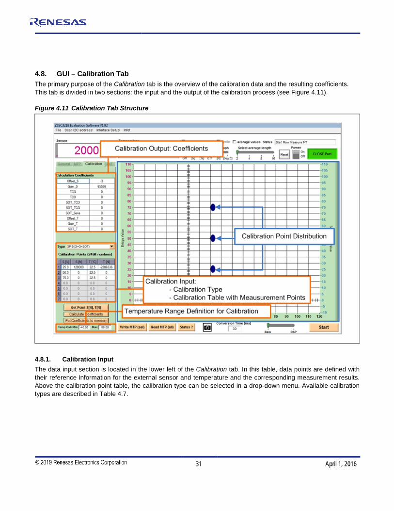
4.8. GUI – Calibration Tab The primary purpose of the Calibration tab is the overview of the calibration data and the resulting coefficients. This tab is divided in two sections: the input and the output of the calibration process (see Figure 4.11).
Figure 4.11 Calibration Tab Structure
4.8.1. Calibration Input The data input section is located in the lower left of the Calibration tab. In this table, data points are defined with their reference information for the external sensor and temperature and the corresponding measurement results. Above the calibration point table, the calibration type can be selected in a drop-down menu. Available calibration types are described in Table 4.7.
ZSSC3218 Evaluation Kit Description
© 2016 Integrated Device Technology, Inc. 32 April 1, 2016
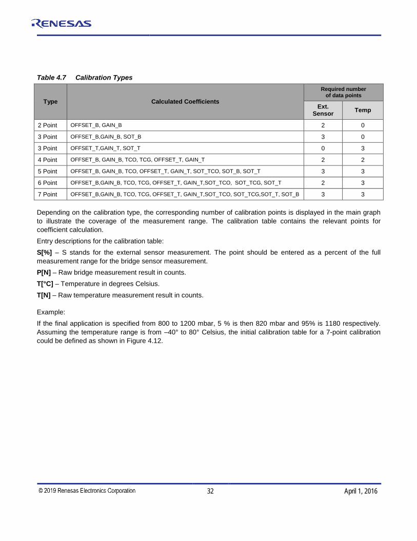
Table 4.7 Calibration Types
Type Calculated Coefficients
Required number of data points
Ext. Sensor Temp
2 Point OFFSET_B, GAIN_B 2 0
3 Point OFFSET_B,GAIN_B, SOT_B 3 0
3 Point OFFSET_T,GAIN_T, SOT_T 0 3
4 Point OFFSET_B, GAIN_B, TCO, TCG, OFFSET_T, GAIN_T 2 2
5 Point OFFSET_B, GAIN_B, TCO, OFFSET_T, GAIN_T, SOT_TCO, SOT_B, SOT_T 3 3
6 Point OFFSET_B,GAIN_B, TCO, TCG, OFFSET_T, GAIN_T,SOT_TCO, SOT_TCG, SOT_T 2 3
7 Point OFFSET_B,GAIN_B, TCO, TCG, OFFSET_T, GAIN_T,SOT_TCO, SOT_TCG,SOT_T, SOT_B 3 3
Depending on the calibration type, the corresponding number of calibration points is displayed in the main graph to illustrate the coverage of the measurement range. The calibration table contains the relevant points for coefficient calculation.
Entry descriptions for the calibration table: S[%] – S stands for the external sensor measurement. The point should be entered as a percent of the full measurement range for the bridge sensor measurement. P[N] – Raw bridge measurement result in counts. T[°C] – Temperature in degrees Celsius.
T[N] – Raw temperature measurement result in counts.
Example: If the final application is specified from 800 to 1200 mbar, 5 % is then 820 mbar and 95% is 1180 respectively. Assuming the temperature range is from –40° to 80° Celsius, the initial calibration table for a 7-point calibration could be defined as shown in Figure 4.12.
ZSSC3218 Evaluation Kit Description
© 2016 Integrated Device Technology, Inc. 33 April 1, 2016
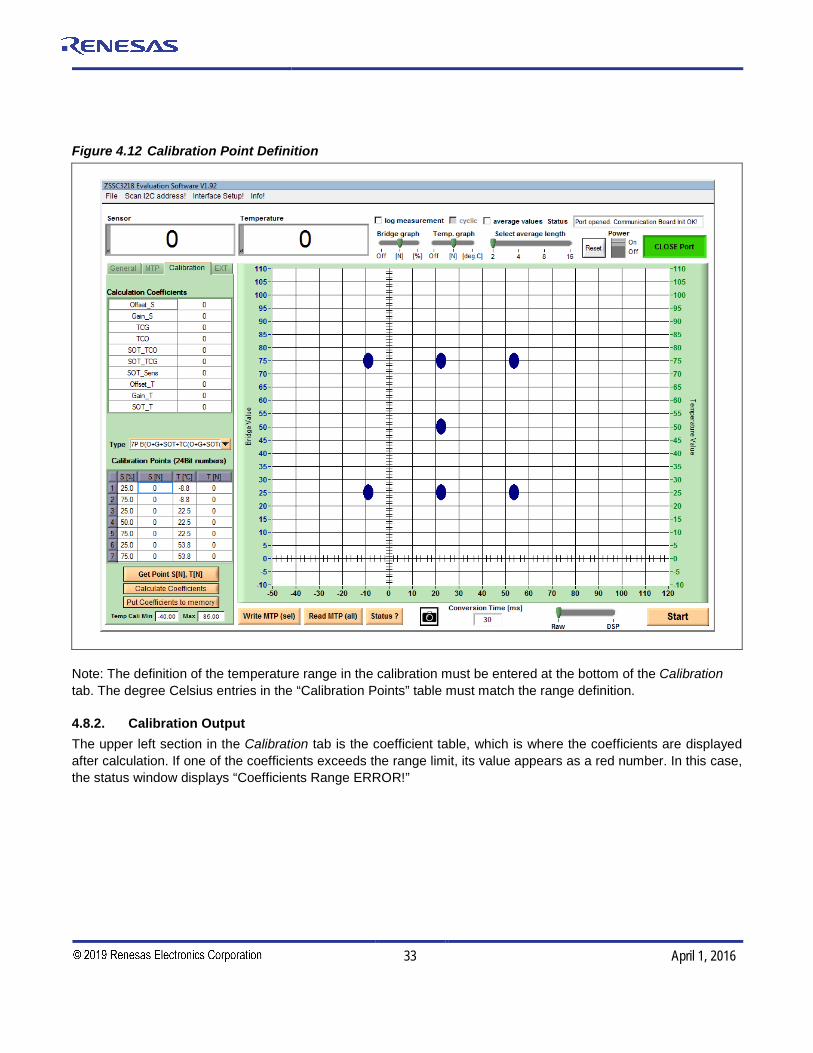
Figure 4.12 Calibration Point Definition
Note: The definition of the temperature range in the calibration must be entered at the bottom of the Calibration tab. The degree Celsius entries in the “Calibration Points” table must match the range definition.
4.8.2. Calibration Output The upper left section in the Calibration tab is the coefficient table, which is where the coefficients are displayed after calculation. If one of the coefficients exceeds the range limit, its value appears as a red number. In this case, the status window displays “Coefficients Range ERROR!”
ZSSC3218 Evaluation Kit Description
© 2016 Integrated Device Technology, Inc. 34 April 1, 2016
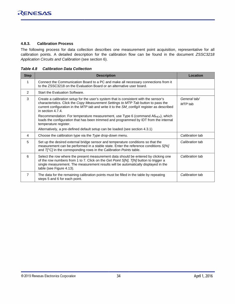
4.8.3. Calibration Process The following process for data collection describes one measurement point acquisition, representative for all calibration points. A detailed description for the calibration flow can be found in the document ZSSC3218 Application Circuits and Calibration (see section 6).
Table 4.8 Calibration Data Collection Step Description Location
1 Connect the Communication Board to a PC and make all necessary connections from it to the ZSSC3218 on the Evaluation Board or an alternative user board.
2 Start the Evaluation Software.
3 Create a calibration setup for the user’s system that is consistent with the sensor’s characteristics. Click the Copy Measurement Settings to MTP Tab button to pass the current configuration in the MTP tab and write it to the SM_configX register as described in section 4.7.4. Recommendation: For temperature measurement, use Type 6 (command A6HEX), which loads the configuration that has been trimmed and programmed by IDT from the internal temperature register. Alternatively, a pre-defined default setup can be loaded (see section 4.3.1)
General tab/ MTP tab
4 Choose the calibration type via the Type drop-down menu. Calibration tab
5 Set up the desired external bridge sensor and temperature conditions so that the measurement can be performed in a stable state. Enter the reference conditions S[%] and T[°C] in the corresponding rows in the Calibration Points table.
Calibration tab
6 Select the row where the present measurement data should be entered by clicking one of the row numbers from 1 to 7. Click on the Get Point S[N], T[N] button to trigger a single measurement. The measurement results will be automatically displayed in the table (see Figure 4.13).
Calibration tab
7 The data for the remaining calibration points must be filled in the table by repeating steps 5 and 6 for each point.
Calibration tab
ZSSC3218 Evaluation Kit Description
© 2016 Integrated Device Technology, Inc. 35 April 1, 2016
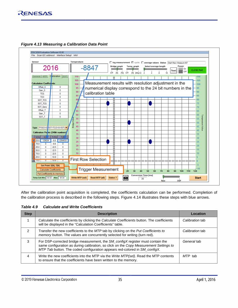
Figure 4.13 Measuring a Calibration Data Point
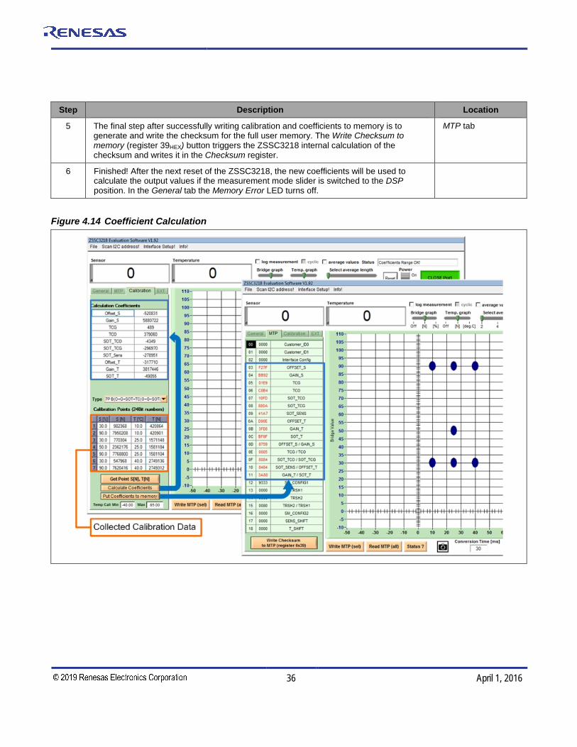
After the calibration point acquisition is completed, the coefficients calculation can be performed. Completion of the calibration process is described in the following steps. Figure 4.14 illustrates these steps with blue arrows.
Table 4.9 Calculate and Write Coefficients Step Description Location
1 Calculate the coefficients by clicking the Calculate Coefficients button. The coefficients will be displayed in the “Calculation Coefficients” table.
Calibration tab
2 Transfer the new coefficients to the MTP tab by clicking on the Put Coefficients to memory button. The values are concurrently selected for writing (turn red).
Calibration tab
3 For DSP-corrected bridge measurement, the SM_configX register must contain the same configuration as during calibration, so click on the Copy Measurement Settings to MTP Tab button. The coded configuration appears red-colored in SM_configX.
General tab
4 Write the new coefficients into the MTP via the Write MTP(sel). Read the MTP contents to ensure that the coefficients have been written to the memory.
MTP tab
ZSSC3218 Evaluation Kit Description
© 2016 Integrated Device Technology, Inc. 36 April 1, 2016
Step Description Location
5 The final step after successfully writing calibration and coefficients to memory is to generate and write the checksum for the full user memory. The Write Checksum to memory (register 39HEX) button triggers the ZSSC3218 internal calculation of the checksum and writes it in the Checksum register.
MTP tab
6 Finished! After the next reset of the ZSSC3218, the new coefficients will be used to calculate the output values if the measurement mode slider is switched to the DSP position. In the General tab the Memory Error LED turns off.
Figure 4.14 Coefficient Calculation
ZSSC3218 Evaluation Kit Description
© 2016 Integrated Device Technology, Inc. 37 April 1, 2016
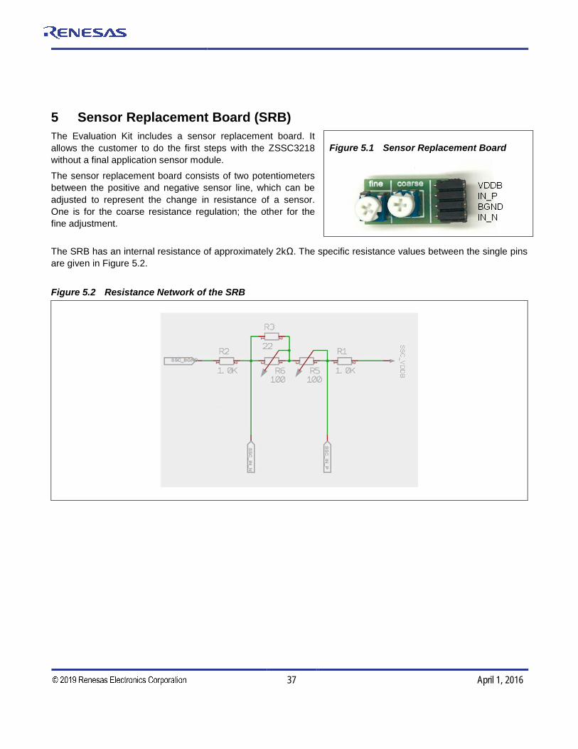
5 Sensor Replacement Board (SRB) The Evaluation Kit includes a sensor replacement board. It allows the customer to do the first steps with the ZSSC3218 without a final application sensor module.
The sensor replacement board consists of two potentiometers between the positive and negative sensor line, which can be adjusted to represent the change in resistance of a sensor. One is for the coarse resistance regulation; the other for the fine adjustment.
The SRB has an internal resistance of approximately 2kΩ. The specific resistance values between the single pins are given in Figure 5.2.
Figure 5.2 Resistance Network of the SRB
Figure 5.1 Sensor Replacement Board
ZSSC3218 Evaluation Kit Description
© 2016 Integrated Device Technology, Inc. 38 April 1, 2016
6 Related Documents and Files
ZSSC3218 Documents
ZSSC3218 Data Sheet
ZSSC33218 Feature Sheet
ZSSC3218 Application Note – Application Circuits
ZSSC3218 Calibration
Visit www.IDT.com/ZSSC3218 and www.IDT.com/ZSSC3218KIT or contact your nearest sales office for the latest version of these documents.
7 Glossary Term Description
A2D Analog-to-Digital
ACK Acknowledge (interface’s protocol indicator for successful data/command transfer)
ADC Analog-to-Digital Converter or Conversion
ALU Arithmetic Logic Unit
AZ Auto-Zero (unspecific)
AZSM Auto-Zero Measurement for External Sensor
AZTM Auto-Zero Measurement for Temperature
CDIP Ceramic Dual-Inline Package
CLK Clock
DF Data Fetch (this is a command type)
DLL Dynamic-Link Library
DUT Device Under Test
DSP Digital Signal Processor (digital configuration, calibration, calculation, communication unit)
FSO Full Scale Output (value in percent relative to the ADC maximum output code; resolution dependent)
LSB Least Significant Bit (“fine” portion of the converted signal)
MSB Most Significant Bit (“coarse” portion of the converted signal)
MTP Multiple-Time Programmable
NACK Not Acknowledge (interface’s protocol indicator for unsuccessful data/command transfer)
PCB Printed Circuit Board
POR Power-On-Reset
ZSSC3218 Evaluation Kit Description
© 2016 Integrated Device Technology, Inc. 39 April 1, 2016
Term Description
PQFN Power Quad Flat No Leads
SM Signal Measurement
SOT Second Order Term
SRB Sensor Replacement Board
TM Temperature Measurement
8 Document Revision History Revision. Date Description
1.00 November 5, 2015 First release. April 1, 2016 Changed to IDT branding.
ZSSC3218 Evaluation Kit Description
© 2016 Integrated Device Technology, Inc. 40 April 1, 2016
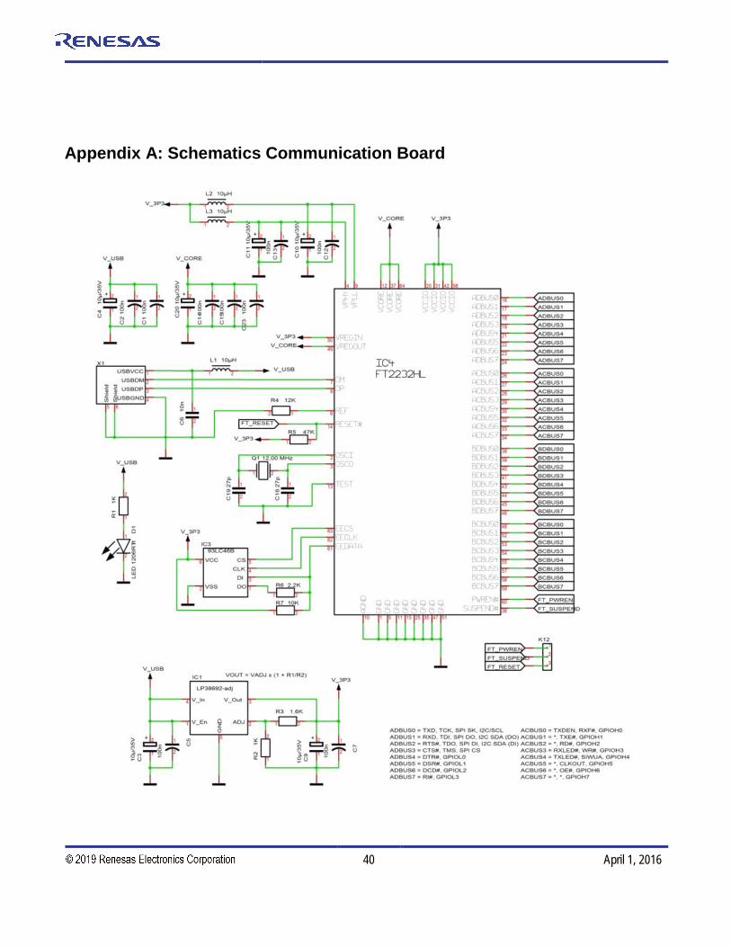
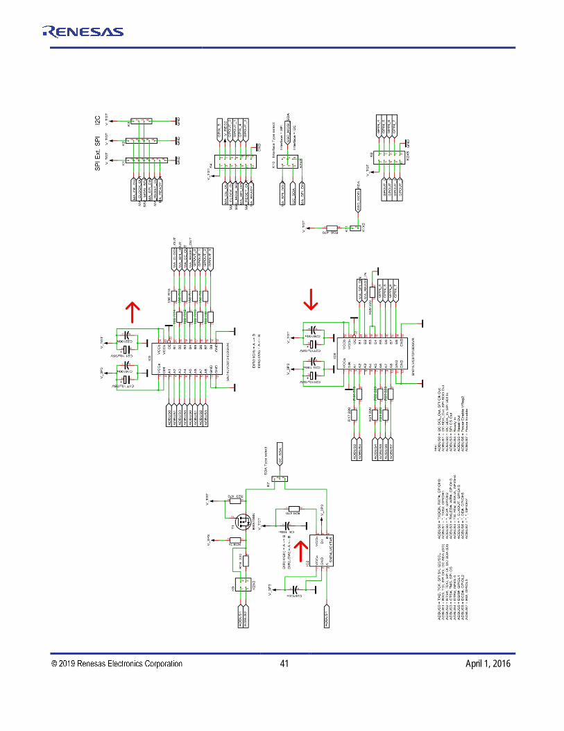
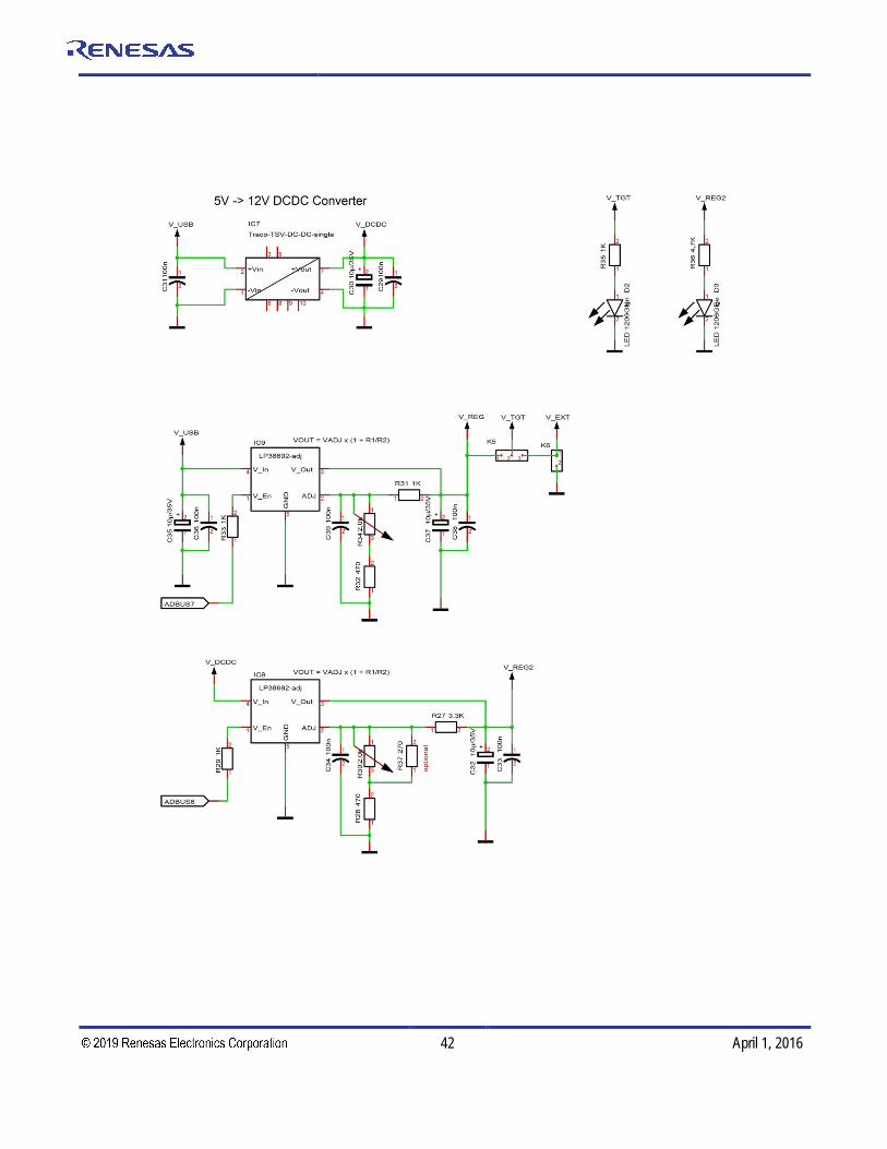
Appendix A: Schematics Communication Board
ZSSC3218 Evaluation Kit Description
© 2016 Integrated Device Technology, Inc. 41 April 1, 2016
ZSSC3218 Evaluation Kit Description
© 2016 Integrated Device Technology, Inc. 42 April 1, 2016
ZSSC3218 Evaluation Kit Description
© 2016 Integrated Device Technology, Inc. 43 April 1, 2016
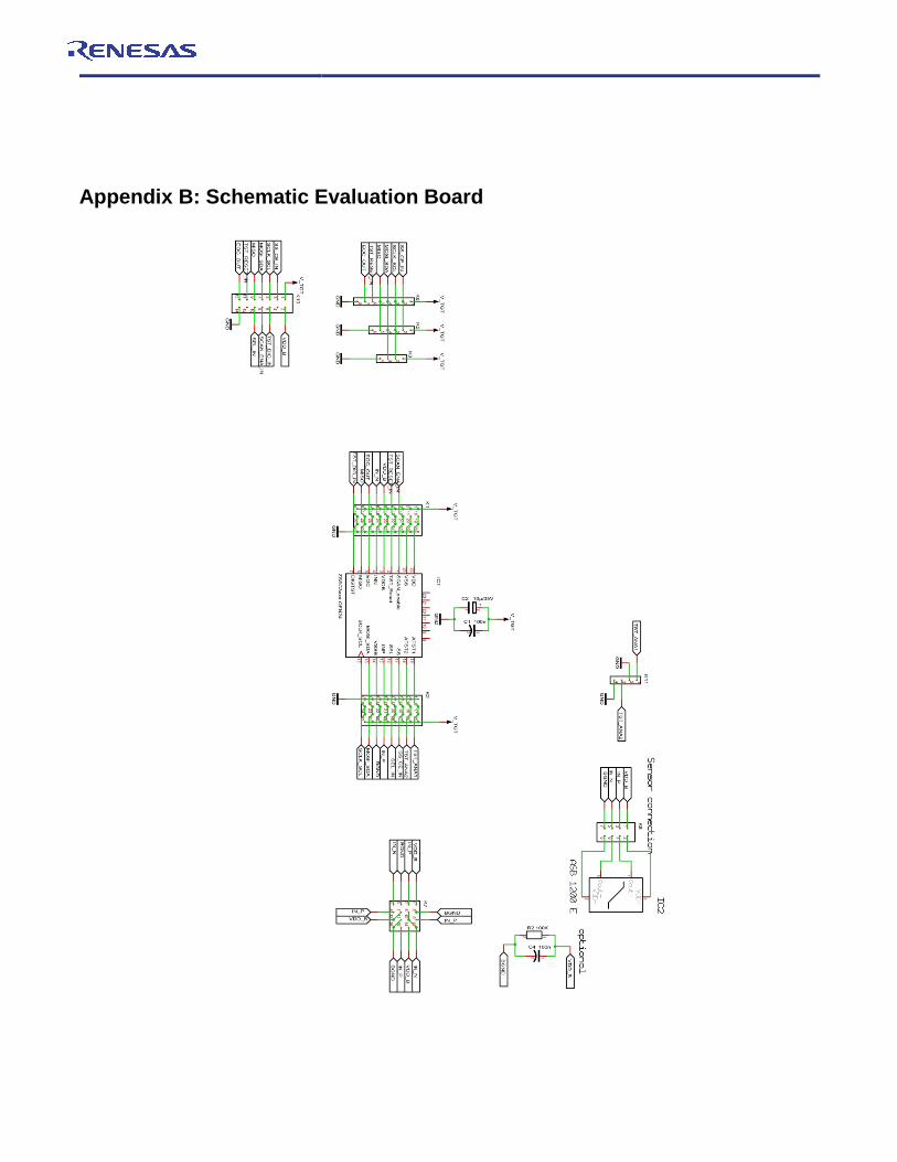
Appendix B: Schematic Evaluation Board

Corporate HeadquartersTOYOSU FORESIA, 3-2-24 Toyosu,Koto-ku, Tokyo 135-0061, Japanwww.renesas.com
Contact InformationFor further information on a product, technology, the most up-to-date version of a document, or your nearest sales office, please visit:www.renesas.com/contact/
TrademarksRenesas and the Renesas logo are trademarks of Renesas Electronics Corporation. All trademarks and registered trademarks are the property of their respective owners.
IMPORTANT NOTICE AND DISCLAIMER
RENESAS ELECTRONICS CORPORATION AND ITS SUBSIDIARIES (“RENESAS”) PROVIDES TECHNICAL SPECIFICATIONS AND RELIABILITY DATA (INCLUDING DATASHEETS), DESIGN RESOURCES (INCLUDING REFERENCE DESIGNS), APPLICATION OR OTHER DESIGN ADVICE, WEB TOOLS, SAFETY INFORMATION, AND OTHER RESOURCES “AS IS” AND WITH ALL FAULTS, AND DISCLAIMS ALL WARRANTIES, EXPRESS OR IMPLIED, INCLUDING, WITHOUT LIMITATION, ANY IMPLIED WARRANTIES OF MERCHANTABILITY, FITNESS FOR A PARTICULAR PURPOSE, OR NON-INFRINGEMENT OF THIRD PARTY INTELLECTUAL PROPERTY RIGHTS.
These resources are intended for developers skilled in the art designing with Renesas products. You are solely responsible for (1) selecting the appropriate products for your application, (2) designing, validating, and testing your application, and (3) ensuring your application meets applicable standards, and any other safety, security, or other requirements. These resources are subject to change without notice. Renesas grants you permission to use these resources only for development of an application that uses Renesas products. Other reproduction or use of these resources is strictly prohibited. No license is granted to any other Renesas intellectual property or to any third party intellectual property. Renesas disclaims responsibility for, and you will fully indemnify Renesas and its representatives against, any claims, damages, costs, losses, or liabilities arising out of your use of these resources. Renesas' products are provided only subject to Renesas' Terms and Conditions of Sale or other applicable terms agreed to in writing. No use of any Renesas resources expands or otherwise alters any applicable warranties or warranty disclaimers for these products.
(Rev.1.0 Mar 2020)
© 2020 Renesas Electronics Corporation. All rights reserved.

Mouser Electronics
Authorized Distributor
Click to View Pricing, Inventory, Delivery & Lifecycle Information: Renesas Electronics:
ZSSC3218KITV1P0