Embed Size (px)
Citation preview

ZnO/metal layered 3D Photonic crystals
Dept. of Physics and Astronomy, Youngstown State University, Youngstown, OH
Michael McMaster, Dr. Tom Oder, Dr. Donald Priour
What to Expect
• What is a Photonic Crystal?• Experimental Procedure • Modeling/Results• Conclusion

• “Photonic crystals are materials patterned with a periodicity in dielectric constant, which can create a range of ‘forbidden’ frequencies called a photonic bandgap. Photons with energies lying in the bandgap cannot propagate through the medium. This provides the opportunity to shape and mould the flow of light for photonic information technology.” – J.D. Joannopoulos, Pierre R. Villeneuve & Shanhui Fan
• Applications include
Photonic Crystal
– Waveguides– LED light extraction– Ultrafast photonic crystal
nanocavity laser
– High speed communication– High speed information
processing
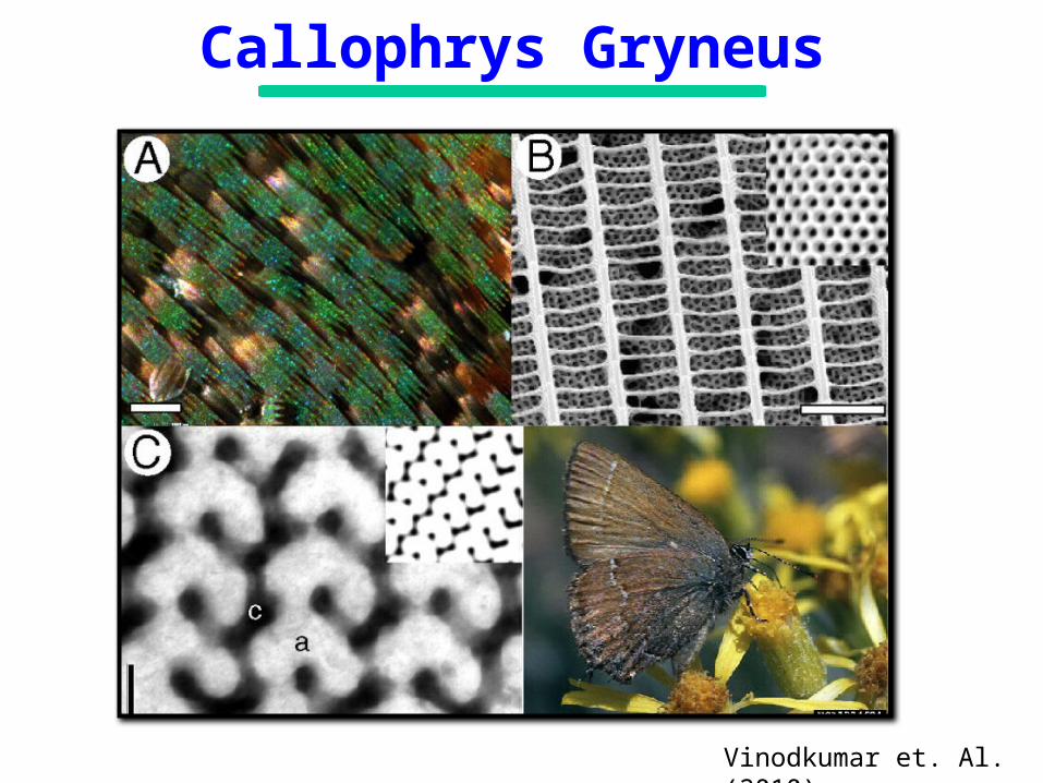
Callophrys Gryneus
Vinodkumar et. Al. (2010)
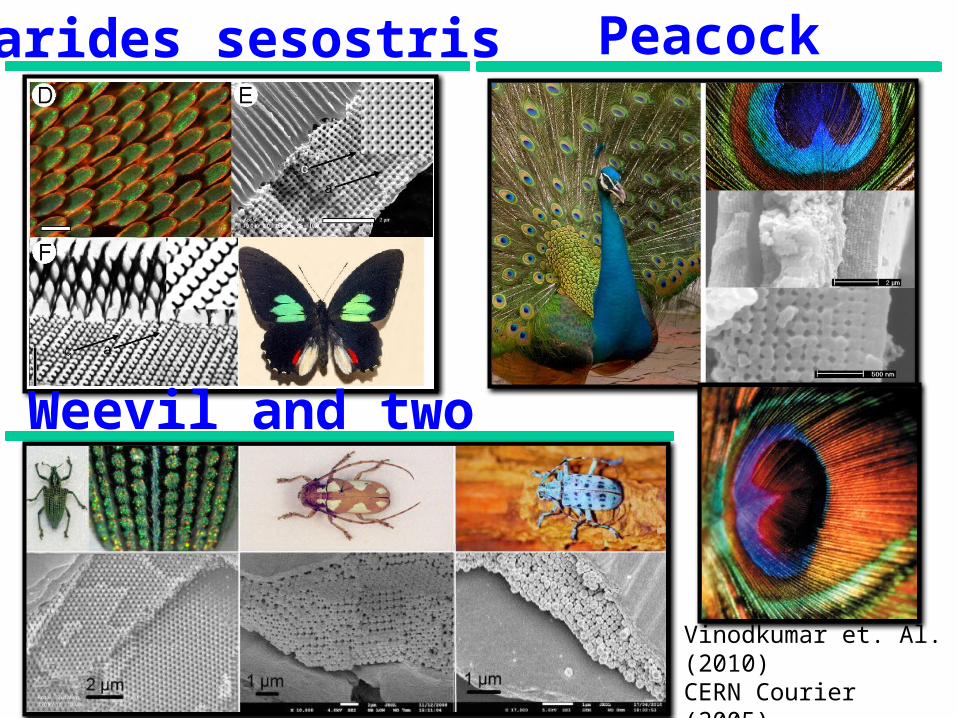
Parides sesostris
Vinodkumar et. Al. (2010)CERN Courier (2005)Vigneron et. Al. (2012)
Peacock
Weevil and two Longhorns
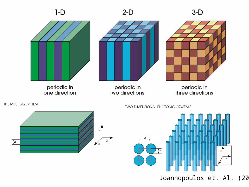
Joannopoulos et. Al. (2008)
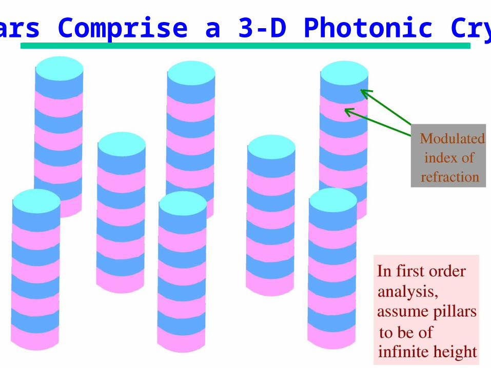
Pillars Comprise a 3-D Photonic Crystal
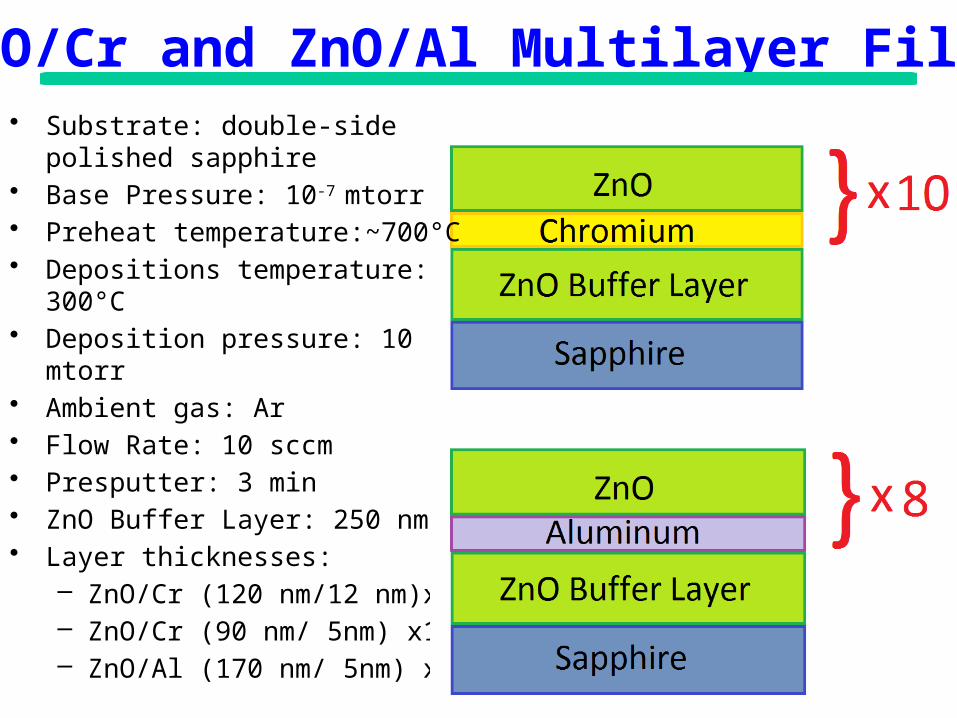
ZnO/Cr and ZnO/Al Multilayer Films• Substrate: double-side polished sapphire• Base Pressure: 10-7 mtorr• Preheat temperature:~700°C• Depositions temperature: 300°C• Deposition pressure: 10 mtorr• Ambient gas: Ar• Flow Rate: 10 sccm• Presputter: 3 min• ZnO Buffer Layer: 250 nm• Layer thicknesses:
– ZnO/Cr (120 nm/12 nm)x10– ZnO/Cr (90 nm/ 5nm) x10– ZnO/Al (170 nm/ 5nm) x8

Bottom Up• Shadow mask sputtering• Periodic Array of Pillars• Quick and easy
Top Down• FIB• Holes in 1-D crystals• Accurate, small feature size
How can we make 3-D Photonic Crystals?
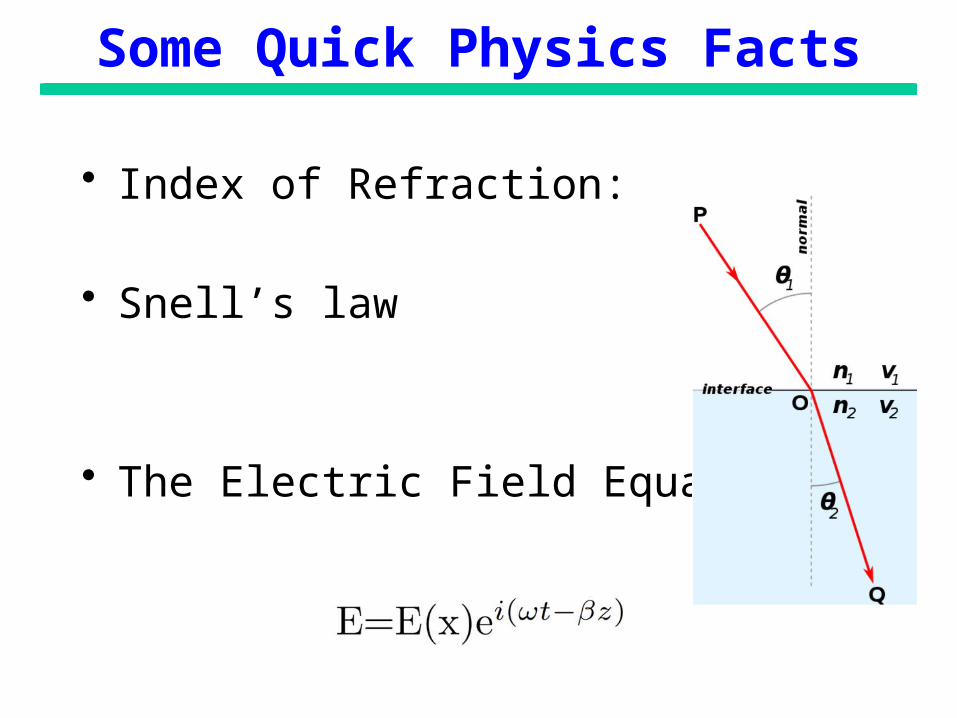
• Index of Refraction:
• Snell’s law
• The Electric Field Equation:
Some Quick Physics Facts
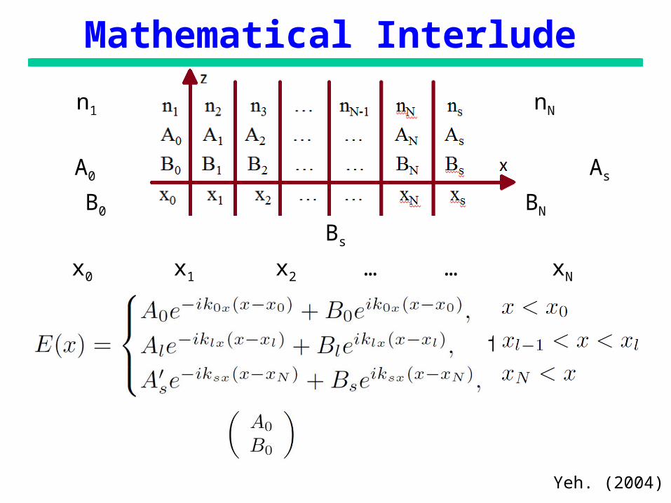
n1 n2 n3 … nN-1 nN ns
A0 A1 A2 … … AN As
B0 B1 B2 … … BN Bs
x0 x1 x2 … … xN xs
The Electric Field can be shown for different refractive indices as:
So we get a vector representing the amplitudes of the wave function.
Mathematical Interlude
Yeh. (2004)
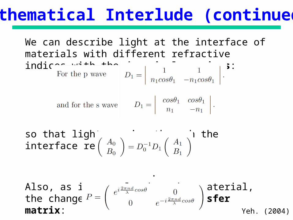
We can describe light at the interface of materials with different refractive indices with the dynamical matrices:
so that light passing through the interface responds such that
.
Also, as it travels through a material, the change is shown by the transfer matrix:
Mathematical Interlude (continued)
Yeh. (2004)

• By acting on the vector representing light passing through the system with the matrices describing the environment we can predict the transmission spectrum.
• Recall:
But metals have an imaginary index of refraction (n) so
let’s write:
But Φ has real an imaginary parts Re(Φ) and Im(Φ) so
where we see the Decay term.
Mathematical Interlude (Recap)
Yeh. (2004)

• Refractive Indices in Visible Spectrum– ZnO 2.0– Cr 3.2– Al 1.3
• Layer thicknesses of samples: – ZnO/Cr (120 nm/12 nm)x10– ZnO/Cr (90 nm/ 5nm) x10– ZnO/Al (170 nm/ 5nm) x8
1-D Photonic Crystals
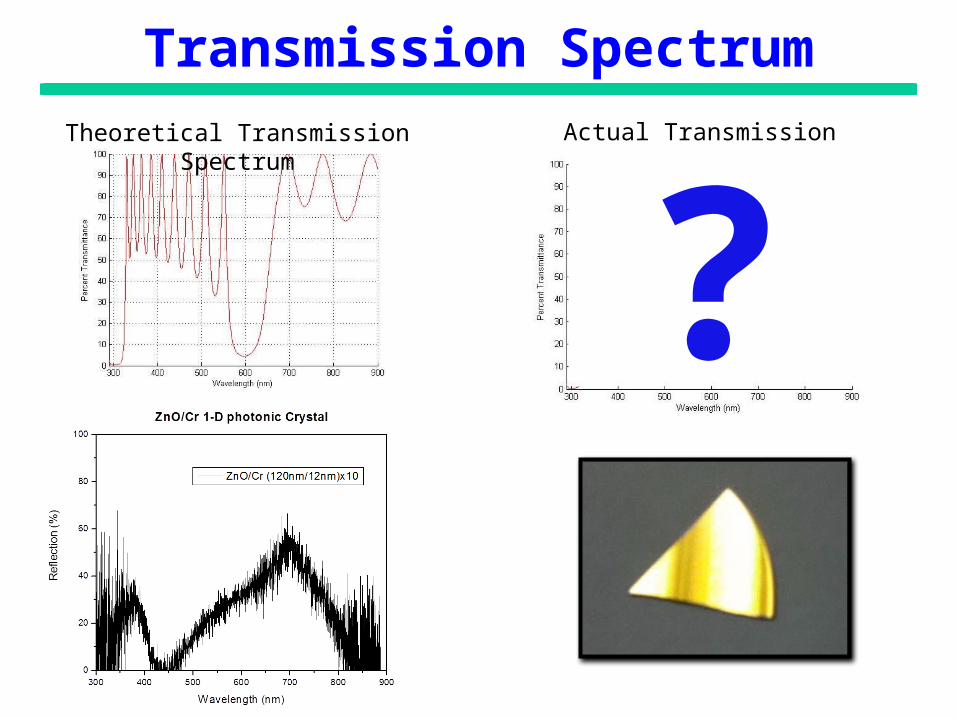
Transmission Spectrum
Theoretical Transmission Spectrum Actual Transmission Spectrum
?
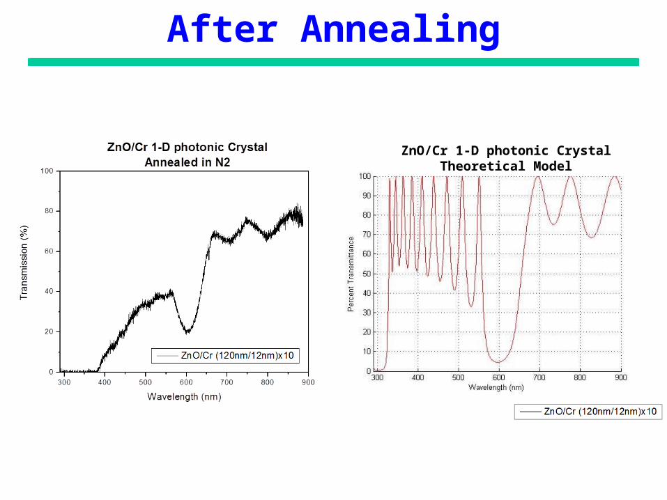
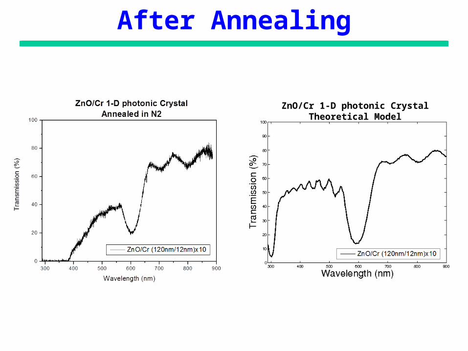
After Annealing
ZnO/Cr 1-D photonic CrystalTheoretical Model
After Annealing
ZnO/Cr 1-D photonic CrystalTheoretical Model

Photonic Crystal
Not a Photonic Crystal
Remember those cosines?
ZnO/Cr (120nm/12nm)x10Theoretical Model

We can Control the Band-Gap!(this Time in Blue)
Band-GapZnO/Cr 1-D photonic CrystalTheoretical Model
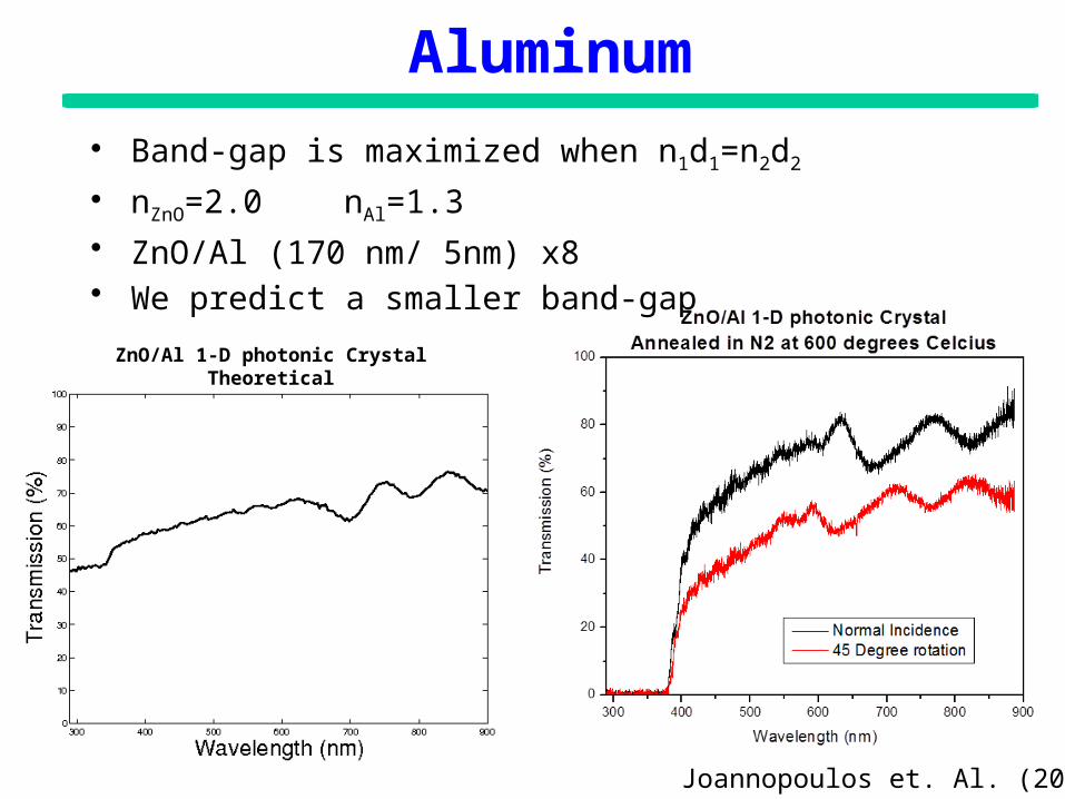
• Band-gap is maximized when n1d1=n2d2
• nZnO=2.0 nAl=1.3
• ZnO/Al (170 nm/ 5nm) x8• We predict a smaller band-gap
Aluminum
Joannopoulos et. Al. (2008)
ZnO/Al 1-D photonic CrystalTheoretical
ZnO/Cr (120 nm/12 nm)x10
ZnO/Cr (90 nm/ 5nm) x10
ZnO/Al (170 nm/ 5nm) x8
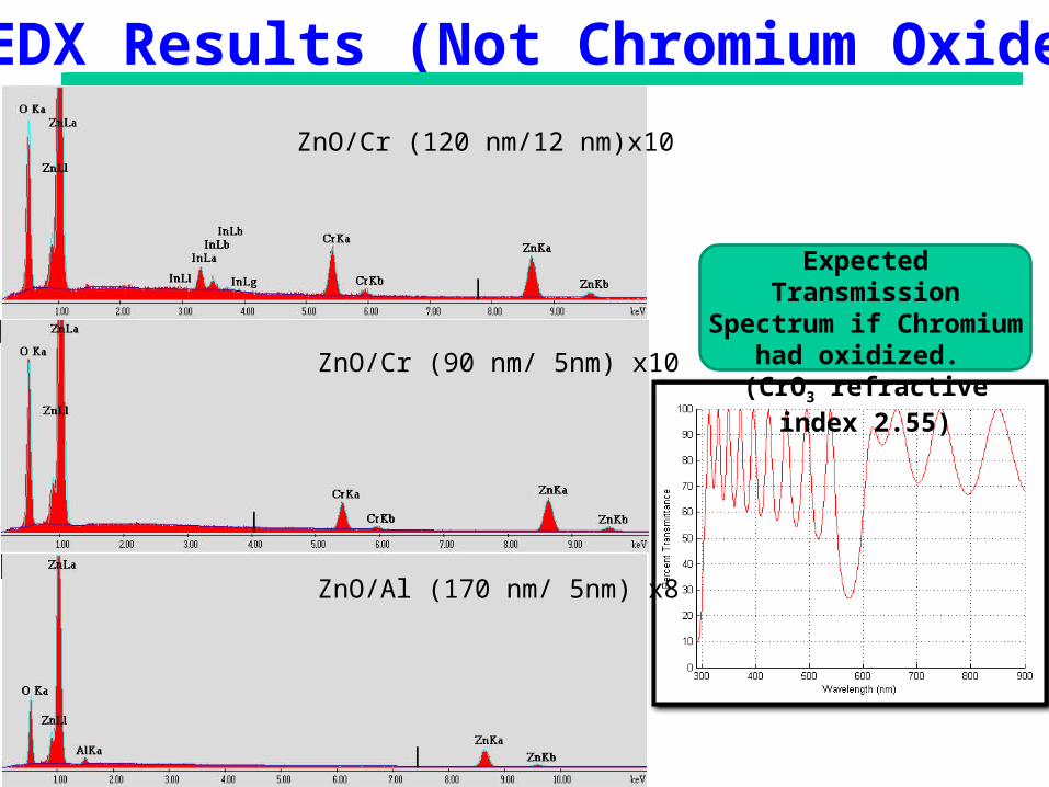
EDX Results (Not Chromium Oxide)
Expected Transmission Spectrum if Chromium had
oxidized. (CrO3 refractive index 2.55)
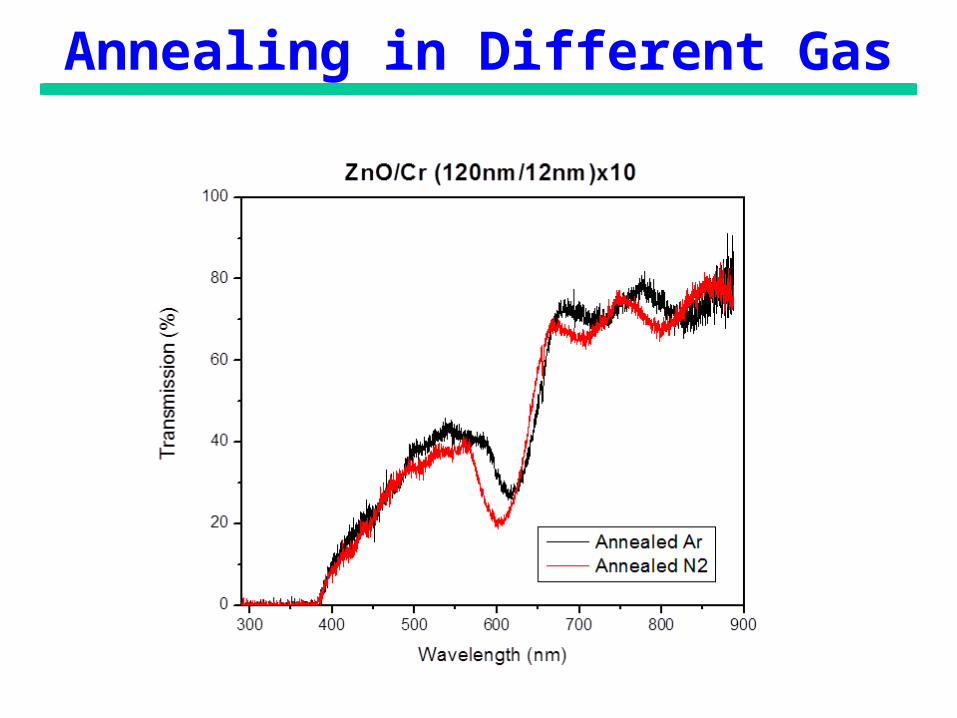
Annealing in Different Gas
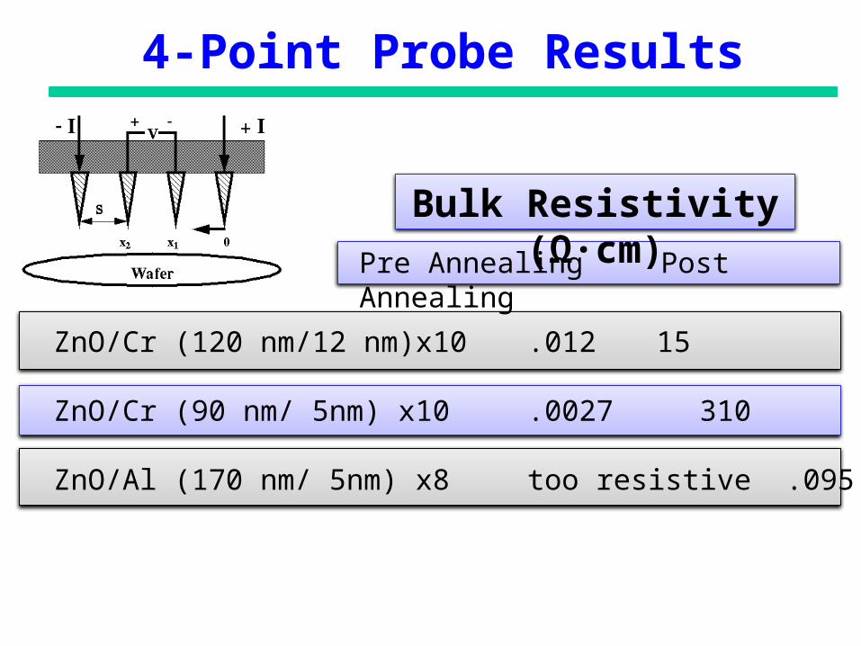
4-Point Probe Results
ZnO/Cr (120 nm/12 nm)x10 .012 15
ZnO/Cr (90 nm/ 5nm) x10 .0027 310
ZnO/Al (170 nm/ 5nm) x8 too resistive .095
Pre Annealing Post Annealing
Bulk Resistivity (Ω∙cm)
• Produce 3-D photonic crystals • using Shadow mask or FIB• Model in higher dimension• TEM/AFM for layer thickness
What Next???
What we Expect
• Evidence of 3-D from diffraction pattern
• Measureable band-gaps in oblique directions
• Improved modeling
What we Hope For
• both polar and radial angle band-gap dependance
• Predict band-gap• Test the effect of electric
field on optical the band-gap
• Vinodkumar Saranathan, Chinedum O. Osuji, Simon G. J. Mochrie, Heeso Noh, Suresh Narayanan, Alec Sandy, Eric R. Dufresne, and Richard O. Prum. Structure, function, and self-assembly of single network gyroid (I4132) photonic crystals in butterfly wing scales PNAS 107 (26) 11676-11681 (2010).
• Joannopoulos, John D., Steven G. Johnson, Joshua N. Winn, Robert D. Meade. Photonic Crystals Modeling the Flow of Light Second Edition. Princeton University Press (2008).
• Yeh, Pochi. Optical Waves In Layered Media: 2nd (second) Edition. Whiley Press (2004).
• Peacock feathers prove photonic crystals cast brown light in nature. CERN Courier. Aug 22, 2005
• Joannopoulos J.D. , Pierre R. Villeneuve and Shanhui Fan. Photonic Crystals: putting a new twist on light. Nature 386 (13) 143-149 (1997)
• Vigneron, Jean Pol, and Priscilla Simonis. Natural photonic crystals. Physica B Condensed Matter 407 (20) 4032-4036 (2012)
References

• We gratefully acknowledge support of funds from NSF (DMR#1006083) and from the State of Ohio (Third Frontier - RC-SAM).
• Support and funds from Youngstown State University
• I would also like to thank Dr. Jim Andrews, Jessica Shipman and Matt Kelly and Dr. George Yates for helping with this project.
Acknowledgements