Embed Size (px)
Citation preview
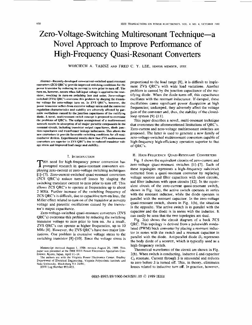
450 IEEE TRANSACTIONS ON POWER ELECTRONICS, VOL. 4. NO. 4, OCTOBER 1989
Zero-Voltage-Switching Multiresonant Technique-a Novel Approach to Improve Performance of High-Frequency Quasi-Resonant Converters
Abstract-Recently-developed zero-current-switched quasi-resonant converters (ZCS QRC’s) provide improved switching conditions for the power transistor by reducing its current to zero prior to turn off. The turn on, however, occurs when full input voltage is applied to the tran- sistor, resulting in turn-on switching loss and noise. Zero-voltage- switched (ZVS) QRC’s overcome this problem by shaping the transis- tor voltage for zero-voltage turn on. In ZVS QRC’s, however, the power transistor suffers from excessive voltage stress and the converter regulation characteristics and stability are adversely affected by par- asitic oscillations caused by the junction capacitance of the rectifying diode. A novel, multiresonant switch concept is proposed to overcome the problems of QRC’s. The unique arrangement of a multiresonant network results in absorption of all major parasitic components in the resonant circuit, including transistor output capacitance, diode junc- tion capacitance and transformer leakage inductance. This allows the new converters to provide favorable switching conditions for all semi- conductor devices. Experimental results show that ZVS multiresonant converters are superior to ZVS QRC’s due to reduced transistor volt- age stress and improved load range and stability.
I. INTRODUCTION HE need for high-frequency power conversion has T prompted research in quasi-resonant converters em-
ploying zero-current or zero-voltage switching techniques [ 11-[7]. Zero-current-switched quasi-resonant converters (ZCS QRC’s) reduce turn-off losses by shaping the switching transistor current to zero prior to turn off. This allows ZCS QRC’s to operate at frequencies up to about 2 MHz. Further increase of the switching frequency of ZCS QRC’s is difficult, due to capacitive turn-on loss, the Miller effect related to turn on of the transistor at nonzero voltage and parasitic oscillations caused by the transis- tor’s output capacitance.
Zero-voltage-switched quasi-resonant converters (ZVS QRC’s) overcome this problem by reducing the switching transistor voltage to zero prior to turn on. As a result, ZVS QRC’s can operate at higher frequencies, up to 10 MHz [8]. However, the ZVS QRC’s have two major lim- itations. One problem is excessive voltage stress to the switching transistor [8]-[ 101. Since the voltage stress is
Manuscript received August 1, 1988; revised August 20, 1989. This paper was presented at the 1988 IEEE Power Electronics Specialists Con- ference, Kyoto, Japan, April 11-14.
The authors are with the Virginia Power Electronics Center, Bradley Department of Electrical Engineering, Virginia Polytechnic Institute and State University, Blacksburg VA 24061.
IEEE Log Number 8931455.
proportional to the load range [8], it is difficult to imple- ment ZVS QRC’s with wide load variations. Another problem is caused by the junction capacitance of the rec- tifying diode. When the diode tums off, this capacitance oscillates with the resonant inductance. If damped, these oscillations cause significant power dissipation at high frequencies; undamped, they adversely affect the voltage gain of the converter and, thus, the stability of the closed- loop system [9]-[ 1 13.
This paper describes a novel, multi-resonant technique that overcomes the aforementioned limitations of QRC’s. Zero-current and zero-voltage multiresonant switches are proposed. The latter is used to generate a new family of zero-voltage-switched multiresonant converters capable of high-frequency high-efficiency operation superior to that of QRC’s.
11. HIGH-FREQUENCY QUASI-RESONANT CONVERTERS Fig. 1 shows the equivalent circuits of zero-current and
zero-voltage quasi-resonant switches [ 11-[7]. Each of these topologies represents a high-frequency subcircuit extracted from a quasi-resonant converter by replacing voltage sources and filter capacitors with short circuits, and filter inductors with open circuits 1121. In the equiv- alent circuit of the zero-current quasi-resonant switch, shown in Fig. l(a), the active switch operates in series with the resonant inductor, while the diode operates in parallel with the resonant capacitor. In the zero-voltage quasi-resonant switch, shown in Fig. l(b), the situation is the opposite. The active switch is in parallel with the capacitor and the diode is in series with the inductor. It can easily be seen that the two topologies are dual.
Fig. 2(a) shows the circuit diagram of a buck ZCS QRC. This topology is derived from a pulsewidth modu- lated (PWM) buck converter by placing a resonant induc- tor in series with the switch and a resonant capacitor in parallel with the diode. Antiparallel diode Ds represents the body diode of a MOSFET, which is typically used as a high-frequency switch.
Theoretical waveforms of the circuit are shown in Fig. 2(b). When switch is conducting, inductor L and capacitor C, resonate. Current through S is sinusoidal and reduces to zero before S is turned off. This, in theory, eliminates losses related to inductive turn off. In practice, however,
0885-8993/89/1000-0450$01 .OO 0 1989 IEEE

45 1 TABISZ AND LEE: PERFORMANCE IMPROVEMENT OF HIGH FREQUENCY QRC’S
) F q D
(a) (b) Fig. 1. Quasi-resonant switches. (a) Zero-current. (b) Zero-voltage
(b) Fig. 2 . Buck ZCS QRC. (a) Circuit diagram. (b) Theoretical waveforms.
reverse recovery of the MOSFET’S body diode causes harm- ful oscillation between the resonant inductor and output capacitance of the MOSFET. To avoid this oscillation, it is necessary to add a diode in series with S to prevent the current from flowing into Ds. The resulting half-wave mode of operation [ l ] not only increases conduction losses, but also makes the converter load-sensitive [2]. The minimum switching frequency at light load is re- duced substantially and leads to larger filter components and slower transient response.
Although ZCS QRC’s take advantage of zero-current tum off, tum on occurs when full input voltage is applied to the switch. This causes dissipation of the energy stored in the output capacitance of the switching transistor and dv/dt noise, which is coupled through the drain-to-gate capacitance of the power MOSFET to the gate-drive circuit (switching Miller effect).
In ZCS QRC’s, the switching conditions for the active device are not the most favorable, but switching condi- tions for the rectifying diode are very desirable. Power diodes are easy to tum on, but the reverse recovery char- acteristics often result in excessive turn-off loss and noise. The most favorable condition to tum off a diode occurs when current reduces gradually to zero and no immediate reverse voltage is applied to the diode afterwards. This is the case for ZCS QRC’s. When S is turned on, the current through D decreases linearly until it reaches zero. The diode then tums off and the voltage across it builds up gradually in a resonant fashion. The only disadvantage is
that the reverse voltage applied across the diode is twice the input voltage. The maximum switching frequency of ZCS QRC’s is limited primarily by the tum-on switching loss in the active switch.
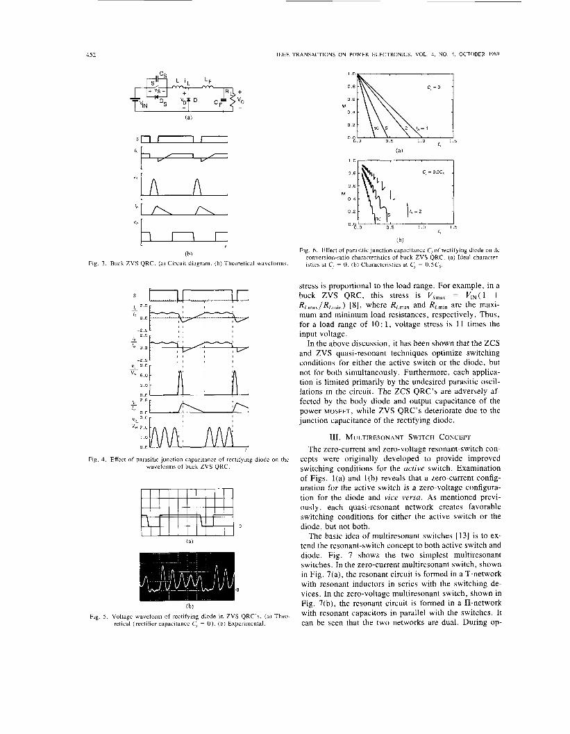
The buck ZVS QRC topology. shown in Fig. 3(a), is derived from its PWM counterpart by adding a resonant capacitor in parallel with the switch and a resonant induc- tor in series with the diode. The inductor can be placed anywhere in the resonant loop, provided the resonant switch, extracted from the circuit, is always reduced to the topology of Fig. l(b). It can be seen, from Fig. 3(b), that the active switch operates under favorable switching conditions. At tum off, the current is diverted from the switch into the resonant capacitor. The capacitor is sub- sequently charged linearly to the input voltage by the load current flowing through L and LF. The gradual increase of zlS minimizes overlapping of the switch current and volt- age at turn off, thus reducing the switching losses. The tum-on condition is even better, since voltage across the switch resonates and reduces the zero prior to turn on. This tum-on condition totally eliminates the capacitive tum-on losses and the switching Miller effect.
Improved switching conditions for the active switch al- low ZVS QRC’s to operate at 10 MHz [8]. However, the operation of ZVS QRC’s is adversely affected by the un- desired switching conditions created for the rectifying diode. It can be seen from Fig. 3(b) that, immediately after the diode current reduces to zero, voltage applied to the diode changes abruptly from zero to VIN. In practice, such an abrupt voltage change induces parasitic oscilla- tions between the resonant inductor and diode capacitance [9], as illustrated in Fig. 4. During conduction of S, the current through the switch and voltage across the diode are oscillatory. In practice, these oscillations typically do not decay before S is turned off, as shown in Fig. 5 . The undesired oscillation adversely affects the conversion ra- tio characteristics, as shown in Fig. 6 for buck ZCS QRC. The conversion ratio M = Vo/VIN is plotted vs. normal- ized frequencyfv = f /fs, where fs = 1 /( 27r Es), with normalized output current Z,v = Z o J L / c s / V I N as a free- running parameter. When junction capacitance C, of the rectifying diode is assumed to be zero, the characteristics are shown as straight lines in Fig. 6(a). Fig. 6(b) shows characteristics for C, = 0.5Cs. It can be seen that, even if C, is only half of the resonant capacitance, its effects are quite pronounced (in high-frequency converters Cj can easily be larger than Cs, especially if high-current diodes with large die areas are used). The discontinuity of the characteristics implies that the zero-voltage-switching property is lost for some operating conditions. Further- more, in regions where the slopes of the curves are posi- tive, the converter exhibits local closed-loop instabilities [ 1 I]. Even in those regions where the slopes are negative, the slope can be very steep, which makes the conversion ratio very sensitive to the switching frequency and, thus, difficult to control.
Another important concern of ZVS QRC’s is extensive voltage stress on the switching transistor. Typically, this
452 IEEE TRANSACTIONS ON POWER ELECTRONICS. VOL 4. NO. 4. OCTOBER 1989
ir b--
I I f
(b) Fig. 3. Buck ZVS QRC. (a) Circuit diagram. (b) Theoretical waveforms.
I
Fig. 4 . Effect of parasitic junction capacitance of rectifying diode on the waveforms of buck ZVS QRC.
(b) Fig. 5 . Voltage waveform of rectifying diode in ZVS QRC’s. (a) Theo-
retical (rectifier capacitance C, = 0) . (b) Experimental.
(b) Fig. 6. Effect of parasitic junction capacitance C, of rectifying diode on dc
conversion-ratio characteristics of buck ZVS QRC. (a) Ideal character- istics at C, = 0. (b) Characteristics at C, = 0.5Cs.
stress is proportional to the load range. For example, in a buck ZVS QRC, this stress is Vs,,, = VIN( 1 + RL,, ,~/RL, , ,~) [8], where RLmax and RLmin are the maxi- mum and minimum load resistances, respectively. Thus, for a load range of 10: 1, voltage stress is 11 times the input voltage.
In the above discussion, it has been shown that the ZCS and ZVS quasi-resonant techniques optimize switching conditions for either the active switch or the diode, but not for both simultaneously. Furthermore, each applica- tion is limited primarily by the undesired parasitic oscil- lations in the circuit. The ZCS QRC’s are adversely af- fected by the body diode and output capacitance of the power MOSFET, while ZVS QRC’s deteriorate due to the junction capacitance of the rectifying diode.
111. MULTIRESONANT SWITCH CONCEPT The zero-current and zero-voltage resonant-switch con-
cepts were originally developed to provide improved switching conditions for the active switch. Examination of Figs. l(a) and l(b) reveals that a zero-current config- uration for the active switch is a zero-voltage configura- tion for the diode and vice versa. As mentioned previ- ously, each quasi-resonant network creates favorable switching conditions for either the active switch or the diode, but not both.
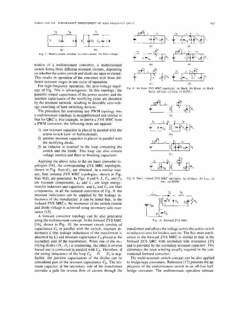
The basic idea of multiresonant switches [13] is to ex- tend the resonant-switch concept to both active switch and diode. Fig. 7 shows the two simplest multiresonant switches. In the zero-current multiresonant switch, shown in Fig. 7(a), the resonant circuit is formed in a T-network with resonant inductors in series with the switching de- vices. In the zero-voltage multiresonant switch, shown in Fig. 7(b), the resonant circuit is formed in a II-network with resonant capacitors in parallel with the switches. It can be seen that the two networks are dual. During op-
TABISZ A N D LEE: PERFORMANCE IMPROVEMENT OF HIGH FREQUENCY QRC'S 453
(a) ib) Fig. 7. Multiresonant switches. (a) Zero-current. (b) Zero-voltage
eration of a multiresonant converter, a multiresonant switch forms three different resonant circuits, depending on whether the active switch and diode are open or closed. This results in operation of the converter with three dif- ferent resonant stages in one cycle of operation.
For high-frequency operation, the zero-voltage topol- ogy of Fig. 7(b) is advantageous. In this topology, the parasitic output capacitance of the power MOSFET and the junction capacitance of the rectifying diode are absorbed by the resonant network, resulting in desirable zero-volt- age switching of both switching devices.
The procedure for converting any PWM topology into a multiresonant topology is straightforward and similar to that for QRC's. For example, to derive a ZVS MRC from a PWM converter, the following steps are applied:
1) one resonant capacitor is placed in parallel with the active switch (uni- or bidirectional),
2) another resonant capacitor is placed in parallel with the rectifying diode,
3 ) an inductor is inserted in the loop containing the switch and the diode. This loop can also contain voltage sources and filter or blocking capacitors.
Applying the above rules to the six basic converter to- pologies [ 141, the corresponding ZVS MRC topologies, shown in Fig. 8(a)-(f), are obtained. In a similar man- ner, four isolated ZVS MRC topologies, shown in Fig. 9(a)-9(d), are generated. In Figs. 8 and 9 , L, C,, and CD are resonant components, LT and CT are large energy- transfer inductors and capacitors, and LF and C, are filter components. In all the isolated converters of Fig. 9, the resonant inductance can be supplied by the leakage in- ductance of the transformer. It can be noted that, in the isolated ZVS MRCs, the resonance of the switch current and diode voltage is achieved using secondary-side reso- nance [ 151.
A forward converter topology can be also generated using the multiresonant concept. In the forward ZVS MRC [16], shown in Fig. 10, the resonant circuit consists of capacitance C, in parallel with the switch, resonant in- ductance L (the leakage inductance of the transformer is absorbed by L ) and resonant capacitance C, placed at the secondary side of the transformer. When one of the rec- tifying diodes ( D , , D 2 ) is conducting, the other is reverse biased and is connected in parallel with C,. Therefore, if the wiring inductance of the loop C, - D , - D2 is neg- ligible, the junction capacitances of the diodes can be considered part of the resonant capacitance C,. The res- onant capacitor at the secondary side of the transformer provides a path for reverse flow of current through the
(a) (d )
LT
(b) (e )
(c) i f,
Fig. 8 . Six basic ZVS MRC topologies. (a) Buck. (b) Boost. (c) Buck- boost. (d) Cuk. (e) Zeta. (0 SEPIC.
(c)
m;(+$ R L
id)
Fig. 9. Basic isolated ZVS MRC topologies. (a ) Flyback. (b) Cuk. (c) Zeta. (d) SEPIC.
L Dq L~
Fig. 10. Forward ZVS MRC
transformer and allows the voltage across the active switch to reduce to zero for lossless tum on. The flux reset mech- anism in the forward ZVS MRC is similar to that in the forward ZCS QRC with secondary-side resonance [ 151 and is provided by the secondary resonant capacitor. This eliminates the reset winding usually required in the con- ventional forward converter.
The multi-resonant switch concept can be also applied to bridge-type converters. Reference [ 171 presents the ap- plication of the multiresonant switch in an off-line half- bridge converter. The multiresonant operation substan-

454 IEEE TRANSACTIONS ON POWER ELECTRONICS. VOL. 4. NO. 4. OCTOBER 1989
tially increases the load range of the converter and im- proves its regulation characteristics compared to the half- bridge ZVS QRC.
V. OPERATION A N D CHARACTERISTICS OF BUCK ZVS MRC
Although a large variety of MRC's exist, their opera- tion and characteristics are similar. The buck ZVS MRC topology is analyzed to gain insight in the operation and performance of ZVS MRC's. Fig. 11 shows a circuit dia- gram of the converter, while Fig. 12 shows its typical waveforms.
During the switching cycle, the converter operates in four topological stages, shown in Fig. 13. The output- filter inductor is assumed to be sufficiently large to be re- placed by current source.
Topological Stage A [to, r l ] This topology arises when the switch is conducting and
the resonant-inductor current is less than Io . This forces differential current Io - iL to flow through rectifying diode D. The resonant-inductor current and the resonant-capac- itor voltages are
N i = -t + i ( t o ) L
Topological Stage B [ f l , t?] When the resonant-inductor current reaches I,, D turns
off and the resonance of L and CD begins. The resonant current and voltages during this mode arc
Topological Stage C [ t z , t3 1 The previous stage ends when S is turned off. Now all
three resonant components form a resonant circuit with current and voltages described by the following expres- sions.
Fig. 1 1 . Circuit diagram of buck ZVS MRC.
BUCK ZVS-MRC
s-
0.0
Fig. 12. Typical waveforms of buck ZVS MRC.
Stage C Stage D
Fig. 13. Topological stages of buck ZVS MRC
CD ( 1 - cos W S D t ) cS + cD

TABISZ AND LEE: PERFORMANCE IMPROVEMENT OF HIGH FREQUENCY QRC'S 455
where
z=&
Topological Stage D [ t3 , t 4 ] This stage begins when voltage vD reduces to zero and
diode D turns on. During this stage, the current and volt- ages of the resonant circuit are
1 . i = [ v,, - vS( t3)] 5 sin wst + i(t3) cos wst (4a)
vs = vS( t3 ) cos wst + Z S i ( t 3 ) sin wst
+ VIN( 1 - cos wst) (4b)
Z/D = 0 (4c)
where
1 ws = - E,
L zs= jG.
The cycle is completed when vs reduces to zero and S turns on starting Stage A.
Equations (1)-(4) are given in their fullest form and can be used to determine the circuit waveforms in each topol- ogical mode with arbitrary initial conditions. The equa- tions are simplified during actual calculations because the initial conditions are frequently zero. The equations were used in a numerical procedure to find the dc conversion- ratio characteristics, shown in Fig. 14(a)-(c). The con-
1 .o
0.6 M
0 . 4
0.2 10
IN = 0.1 7
(c)
Fig. 14. Effect of ratio C,/C, on the conversion-ratio characteristics of buck ZVS MRC. (a) C,/C, = 1 . (b) C D / C , = 2 . (c) C,/C, = 5.
version ratio
( 5 )
is shown as a function of the normalized switching fre- quency
f f N I f s
where f, = w s / ( 27r). Normalized output current
( 7 )
is a free-running parameter. Figure 14(a) shows conversion-ratio characteristics for
a converter with C D / C , = 1. For heavy loads, I , > 1, the characteristics are similar to those of a buck ZVS QRC, as shown in Fig. 6(b). However, for light loads, ZN I 1, the characteristics are quite different. Although in a limited range, the ZVS MRC achieves zero-voltage switching even for very light loads, which is manifested by the presence of the characteristics for IN I 1. When ratio C D / C s is increased, zero-voltage switching is achieved for a wider range of operating conditions, as shown in Fig. 14(b) for C D / C , = 2 and in Fig. 14(c) for
If the switching frequency is limited to a certain range, it is possible to assure that the operating point is always
cD/cs = 5 .

456 IEEE TRANSACTIONS ON POWER ELECTRONICS. VOL. 3. NO. 4. OCTOBER 1989
1
L , r l , ' . 4 ' ' ' ' ' ' ' I oD.5 0 . 6 0 . 7 0.8 0 .9 1.0 1 . 1 1 .2
ft.
(b) Fig. 15. Operating-point loci for buck ZVS MRC with M = 0.5 and I,v
varying from 0 to 1.66 superimposed on its characteristics: (a) DC con- version ratio. (b) Transistor voltage stress. C,/C,7 = 3 .
within the region where the characteristics have a nega- tive slope. This allows the ZVS MRC's to overcome the instability found in ZVS QRC's. For example, Fig. 15(a) shows dc conversion ratio characteristics of a buck ZVS MRC with CD/Cs = 3 for a limited range of switching frequency, fN > 0.5. The line superimposed on the char- acteristics depicts the locus of the operating point for M = 0.5 and IN varying from 0.01 to 1.66. Fig. 15(b) shows corresponding plots of voltage stress applied to the active switch. The voltage stress is less than 3 v 1 ~ for all loads at M = 0.5.
The relatively low voltage stress with a very wide load range is one of the salient features of ZVS MRC's. Fig. 16 shows typical normalized transistor voltage stress in a buck ZVS QRC (dotted lines) and a buck ZVS MRC (solid line). The voltage stress in the quasi-resonant converter is proportional to the load range. For the converter with 10: 1 load range (top dotted line), the voltage stress at full load is 11 times the input voltage. The multiresonant con- verter achieves operation from no load to full load with the voltage stress of approximately three times the input voltage.
Although it appears that the most practical mode of op- eration of ZVS MRC's is that with zero-voltage and non- zero-current switching of the active switch, some other operating modes are possible. One interesting mode of operation is described below.
It is observed that, during Topological Stage B, the equivalent resonant circuit is identical to that of ZCS
0 1 ~
PO",,,
Fig. 16. Comparison of transistor voltage stress in buck ZVS QRC (dotted lines) and buck ZVS MRC (solid line).
-2.5
vs 3.0 - v,, 2 .o
I .o
0.0 jo 2 . 5
c vg 3.0
-
0.0
-
Fig. 17. Theoretical waveforms of buck ZVS MRC at C,l/C,7 = I . I , =
l , f N = 0.5, and M = 0.5. At these operating conditions both transistor and diodc have almost perfect switching conditions.
QRC's, shown in Fig. l(a). Similarly, during Topological Stage D, the resonant circuit is identical to that of ZVS QRC's, shown in Fig. l(b). As explained previously, in ZCS QRC's the transistor switches at zero current, while the diode switches at zero-voltage. In ZVS QRC's, the transistor switches at zero voltage, while the diode switches at zero current. An interesting question arises as to whether it is possible, using the multiresonant switch, to provide switching conditions where both the current and voltage are simultaneously zero for both the transistor and diode, at both turn on and tum off. Although such an ideal operation has not been achieved, it was proven fea- sible to operate ZVS MRC's with switching conditions close to ideal. Fig. 17 shows waveforms of a buck ZVS MRC with CD/Cs = 1, IN = I . f N = 0.5, and M = 0.5. It can be seen that both the transistor and diode operate with almost perfect zero-current and zero-voltage switch- ing. This mode of operation would be extremely desirable at high frequencies. However, to operate the circuit in this fashion it is necessary to keep all operating conditions fixed, which reduces its practical value. This unusual

TABISZ A N D LEE: PERFORMANCE IMPROVEMENT OF HIGH FREQUENCY QRC’S 457
Cs .. 2°F
‘1 I
I A - -
Fig. 18. Circuit diagram of experimental buck ZVS MRC
(C) (d)
Fig. 19. Waveforms of experimental buck ZVS MRC at different output- power levels: (a) 20 W . (b) 12.5 W. (c) 7 .5 W. (d) 1.5 W. Top wave- form: resonant inductor current ( 5 A/d iv ) . middle waveform: drain-to- source voltage of Q, ( 2 0 V / d i v ) . bottom waveform: rectifying diode voltage ( 2 0 V/d iv ) .
mode of operation was verified experimentally, but the converter was very sensitive to the operating conditions and difficult to control.
VI. EXPERIMENTAL RESULTS Fig. 18 shows a complete circuit diagram of an exper-
imental buck ZVS MRC with a single-loop control. The error voltage produced by the op-amp was used to control the voltage-controlled oscillator (VCO) (gates B and C), which provided constant off-time and variable on-time for Q,. MOSFET Q , was driven by a quasi-resonant gate drive described in detail in [8]. The control circuit was not op- timized for best dynamic performance at present.
The converter was designed for CD/Cs = 3 and oper- ated with VI, = 15 V , V , = 7.5 V and a maximum output power of 20 W . Fig. 19 shows experimental waveforms of the converter for various output-power levels. The measurement results are shown in Table I. The converter
4.30 2.67 1.77 20.03 26.55 75.4 37.0 4.30 4.72 2.00 1.39 15.00 20.85 71.9 35.5 3.90 5.20 1.36 1.06 10.20 15.90 64.2 33.0 3.50 5.62 0.66 0.64 4.95 9.60 51.6 30.0 3.05 7.33 0.10 0.11 0.75 1.65 35.5 18.0 1.25
operated at 4 .3 MHz at full load with an efficiency of 75.4 percent. At an output power of 0.75 W (3.75 percent of full load), switching frequency increased to 7.33 MHz. Taking into consideration this wide load range, the range of frequency modulation is relatively narrow. The voltage stress was less than 37 V for all loads. The maximum current stress to the transistor was 4.3 A at full load. This current stress is approximately 1.6 times higher than that of a buck ZVS QRC, resulting in increased conduction losses. However, substantial reduction of the voltage stress achieved by multiresonant operation allows usage of MOSFET’S with lower breakdown voltage and lower on- resistance. This helps to reduce conduction losses. The exact analysis of the stresses in MRC’s remains to be per- formed.
A 50-W forward ZVS MRC was also implemented with an input voltage of 50 V and an output voltage of 5 V. The converter operated with 0-100 percent load range, an efficiency of 80 percent at full load and frequency ranging from 4 . 3 MHz at full load to 5.3 MHz at no load. Zero- voltage-switching was maintained for all loads with max- imum voltage stress to the switching transistor of 200 V.
VII. CONCLUSION A novel, multiresonant switch concept is proposed to
overcome the limitations of high-frequency quasi-reso- nant converters. A new family of zero-voltage-switching multiresonant converters is generated. The new convert- ers operate with favorable zero-voltage switching condi- tions for both the transistor and rectifying diode. Transis- tor voltage stress in ZVS MRC’s is significantly reduced, compared to that in ZVS QRC’s, while the load range is dramatically improved. Due to the unique arrangement of the resonant circuit in ZVS MRC’s, it absorbs all major parasitic reactances, including transistor output capaci- tance, diode junction capacitance and transformer leakage inductance. By limiting the switching frequency range, the ZVS MRC’s can avoid instability found in ZVS QRC’s caused by the parasitic oscillation between the junction capacitance of the rectifier and the resonant in- ductance. Since the junction capacitance of the rectifier is used as a part of the resonant circuit, high-current diodes with large junction capacitance can be used to reduce con- duction losses in the rectifier. The initial experimental re- sults indicate that the ZVS MRCs are suitable for high- density onboard and off-line power supplies operating above one MHz.
458 IEEE TRANSACTIONS ON POWER ELECTRONICS. VOL 3. NO. 4. OCTOBER 1989
REFERENCES [ I ] K. H. Liu and F. C. Lee, “Resonant switches-A unified approach
to improve performance of switching converters,” IEEE Internu- tional Telecommunications Energy ConJ Proc., 1984, pp. 334-341,
121 K . Liu, R. Oruganti, and F. C. Lee, “Resonant switches-Topolo- gieS and characteristics,” IEEE Trans. POwer Electron., vol. 2, no.
[ 141 K . H . Liu, F. C . Lee, ”Topological constraints on basic PWM con- verters,” IEEE Power Elecrronics Specialists Conf. Rec.. 1988. pp. 164-1 72.
[ IS] K . H. Liu and F. C. Lee, “Secondary-side resonance for high-fre- quency power conversion.” IEEE Applied Power Elecrronics Coiif. Proc., 1986, pp. 83-89.
[16] W. A. Tabisz and F. c. L ~ ~ , “A novel . z~ro-voltage.switched m u l t i - I , pp. 62-74, Jan. 1987. K. H. Liu and F. C. Lee, “Zero-current-switched quasi-resonant con- verters operating in full-wave mode,” U. S . Patent 4720667. Jan. 1988. P. C. Todd and R. W. Lutz, “Practical resonant power converters- Theory and application: Part 11-The resonant switch concept,” Pow- ertech. Mag., May 1986. K. H. Liu and F. C. Lee, “Zero-voltage switching technique in dc i dc converters.’’ IEEE Power Electronics Specialisrs Conf. Rec., 1986. pp. 58-70. M. K . Kazimierczuk and J . Joiwik, “New topologies of high-effi- ciency high-frequency zero-voltage-switching resonant dc i dc con- verters,” 29th Midwesr Symp. Circuits and Sysrems Proc., 1986, pp. 474-477. K . H. Liu and F. C. Lee, “Zero-voltage-switched quasi-resonant converters,’’ U. S. Patent 4720668, Jan. 1988. W. A. Tabisz, P. Gradzki, and F. C. Lee, “Zero-voltage-switched quasi-resonant buck and flyback converters-Experimental results at 10 MHz,” IEEE Trans. Power Electron., vol. 4 , no. 2 , pp. 194-204, April 1989. L. F. Casey, M. F. Schlecht, “A high frequency, low volume, point of load power supply for distributed power systems,” IEEE Trans. Power Electron., vol. 3 , no. 1, pp. 72-82, Jan. 1988. M. F. Schlecht, L. F. Casey, “Comparison of the square-wave and quasi-resonant topologies,” IEEE Trans. Power Electron., vol. 3, no. 1, pp. 83-92, Jan. 1988. M. M. JovanoviC, F. C. Lee, “DC characteristics and stability of push-pull and bridge-type zero-current-switched quasi-resonant con- verters,” IEEE Trans. Power Electron., vol. 4 , no. 3 , July 1989. K . D. T. Ngo, “Generalization of resonant switches and quasi-reso- nant dc-dc converters,’’ IEEE Power Electronics Specialists Conf. Rec., 1987, pp. 395-403. W. A. Tabisz and F. C. Lee, “Application of a novel, multi-resonant switch in high-frequency dc idc converters.” Virginia Power Elec- tronics Cenrer Seminar Proc., Virginia Polytechnic Institute and State University, Blacksburg, VA, 1987, pp. 65-71.
resonant forward converter,’’ High Frequency Poww Conversion Conf. Proc., 1988, pp. 309-318.
(171 M. M . JovanoviC, W. A. Tabisz, and F. C. Lee, “Zero-voltage- switching technique in high-frequency off-line converters,” IEEE Trans. Power Electron.. vol. 4, no. 4, pp.
Wojciech A. Tabisz received the M.S. degree in electronics engineering from the Department of Electronics, Technical University of Warsaw, Warsaw, Poland, in 1984. Currently, he is work- ing towards the Ph.D. degree at the Bradley De- partment of Electrical Engineering, Virginia Polytechnic Institute and State University. Blacksburg, VA.
He is presently a Project Assistant at the Vir- ginia Power Electronics Center, VPI&SU. He has been recently involved in the development of low-
profile, high-density on-board power supply technology. His main research interests are high-frequency power conversion. resonant converter topol- ogy, power semiconductor devices, and computer-aided analysis and de- sign. He has published 14 conference and transactions papers and four in- dustry and government reports on power electronics.
Fred C. Y. Lee (S’72-M’74-M’77-SM’87), for a photograph and biog- raphy please see page 390 of this issue.