Embed Size (px)
Citation preview
IEEE TRANSACTIONS ON INDUSTRY APPLICATIONS, VOL. 29, NO. 1, JANUARYFEBRUARY 1993 113
Pulse Width Modulation with Resonant dc Link Converters
Giri Venkataramanan, Member, IEEE, and
Abstract- A technique for realizing pulse width modulation (PWM) capability in resonant dc link converters is presented in this paper. This technique eliminates the subharmonics present in the conventional discrete pulse modulated converters without re- quiring any additional switching devices. Detailed design-oriented analysis enumerating the tradeoffs involved are presented. Con- trol techniques for simultaneously accomplishing link and output control are considered. Simulation results verifying the principle of operation are presented and backed up by experiments.
I. INTRODUCTION HE ADVENT OF higher switching frequencies is an T inevitable trend in the area of power converters. This
stems from the smaller filters, higher power density, low acoustic noise, and improved transient response resulting from the increase in switching frequency. The availability of high- performance devices such as IGBT’s in recent years has raised the expectation of correspondingly higher performance from pulse width modulated (PWM) inverters used in multikilowatt (2-500 kW) adjustable-speed drive and UPS applications. The performance of IGBT inverters is severely limited by two factors: the switching loss in the devices and the high d v / d t on the output of the inverter. The limitation due to the first is well known and limits the switching frequency to 4-8 kHz, unless excessive derating of device current ratings is incurred. At a frequency of 20 kHz, which is normally considered to be a desirable lower limit, the switching loss in an IGBT could be as high as four times the conduction loss in the device [ 11. The second factor, i.e., the d v / d t on the output, is receiving greater attention in the literature. The d v / d t for IGBT’s could be as high as 10 000 V/p s and could be the source of conducted and radiated EMI. There have also been documented cases of motor insulation breakdown in the presence of such steep wavefronts. The International Electrotechnical Commission (IEC) has a working group investigating the possibility of limiting the d v / d t to less than 500 V/p s [2].
It is not surprising that in the face of problems related to “hard switching,” i.e., high switching loss and high d v l d t , soft switching inverters have attracted great interest in industry.
Paper IPCSD 91-83, approved by the Industrial Power Converter Committee of the IEEE Industry Applications Society for presentation at the 1990 Industry Applications Society Annual Meeting, Seattle, WA, Oct. 7-12. This work was supported by the University of Wisconsin-Graduate School for Funding given under the Technology Innovation Fund. Manuscript released for publication May 29, 1991.
D. M. Divan is with the Department of Electrical and Computer Engineer- ing, University of Wisconsin, Madison, WI 53706.
G. Venkataramanan is with the Department of Electrical Engineering, montana State University, Bozeman, MT 59717.
IEEE Log Number 9204187.
Deepakraj M. Divan, Senior Member, IEEE
Soft switching inverters, in particular, zero voltage switching topologies, offer virtually zero switching loss and moderate d v / d t stresses. One of the most successful and popular soft switching topologies is the resonant dc link inverter, this is a circuit that has been shown to be viable in both its voltage and current source versions [3]-[7]. Frequencies in the order of 65 kHz at a power level of 40 kVA have been demonstrated, with potential for applications in the 200-kVA range [8].
The biggest problem facing the family of resonant link inverters stems from the need for discrete pulse modulation (DPM). Low switching loss is typically realized by turning devices on and off when the bus voltage is zero which is an event that occurs almost periodically at a rate given by the bus oscillation frequency. The constraint of switching at bus zero crossings create energy at frequencies substantially below the link frequency. In the case of PWM inverters, the harmonics occur only at side bands around multiples of the switching frequency and are, thus, well constrained. The possibility of realizing true PWM capability in resonant link inverters is thus a desirable objective, as it could preserve the advantages of zero losses, high-switching frequency, and elimination of subharmonic energy content. Malesani and Divan [9] presented a synchronous PWM resonant dc link inverter raising the possibility of true PWM operation. However, as the resonant bus interval could be modulated above a minimum value, control in a three-phase inverter was seen to be rather limited. Another approach that combined a conventional resonant dc link inverter stage with a single-phase soft-switched PWM input stage was presented in [lo]. This paper presents an extension of that technique to three-phase systems utilizing essentially the same topology as the conventional poly-phase resonant dc link inverter but allowing true PWM over a fairly wide operating range. The paper investigates operating characteristics, design tradeoffs, and design methodology for this type of converter and does a detailed comparison with resonant link and conventional PWM inverters. Operation of the proposed inverter is also confirmed experimentally.
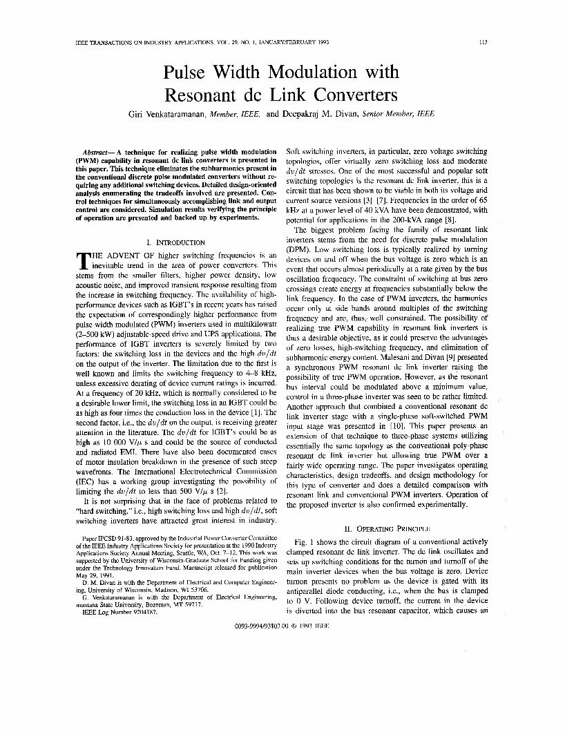
11. OPERATING PRINCIPLE Fig. 1 shows the circuit diagram of a conventional actively
clamped resonant dc link inverter. The dc link oscillates and sets up switching conditions for the tumon and turnoff of the main inverter devices when the bus voltage is zero. Device tumon presents no problem as the device is gated with its antiparallel diode conducting, i.e., when the bus is clamped to 0 V. Following device turnoff, the current in the device is diverted into the bus resonant capacitor, which causes an
0093-9994/93$03.00 0 1993 IEEE
114 IEEE TRANSACTIONS ON INDUSTRY APPLICATIONS, VOL. 29, NO. 1, JANUARYIEBRUARY 1993
Y f Motor
Fig. 1. Circuit schematic of a three-phase actively clamped resonant dc link inverter.
Fig. 2. Circuit schematic of a three-phase actively clamped dc link converter with capacitors across all devices.
initiation of the next resonant cycle. It should be noted that the bus resonant capacitor C, is typically connected in a distributed fashion across the bus. In some cases, in particular with GTO inverters, some of the capacitance may also be connected across individual devices to provide local snubbing [ 111. All these connections are essentially identical in terms of resonant link performance.
Fig. 2 shows an equivalent connection for the actively clamped resonant dc link inverter in which the bulk of the bus equivalent capacitor is connected across individual devices. During a resonant cycle, the equivalent capacitance across the bus is %Cd, where c d is the capacitance across each individual device. This inverter can be operated in the same manner as the circuit in Fig. 1. However, it can be seen that whenever an active device, say 5’1, is conducting, turnoff can be initiated even during the resonant cycle. The current transfers from the device SI to the effective snubber capacitor across it and causes the voltage across it to build up until the diode D4 in antiparallel with the device S4 is turned on. It should be noted that this turnoff is a soft switching event, which is a result of the capacitance across the device. As may be expected, device turnon requires that the voltage across the device be reset to zero. This is seen to occur due to the action of the resonant link clamp that causes a completion of the bus resonant cycle in the manner associated with resonant link operation. It is clear that there are constraints that need to be satisfied to ensure that the resonant cycle can be completed, and these will be addressed in the next section.
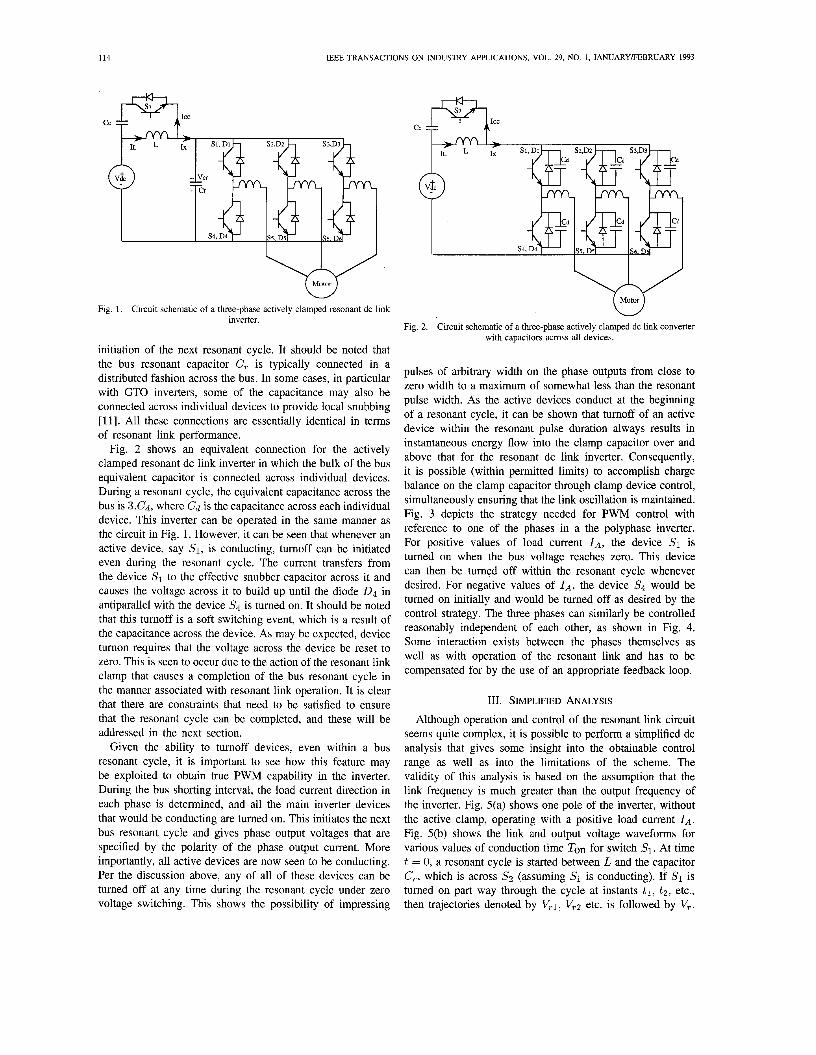
Given the ability to turnoff devices, even within a bus resonant cycle, it is important to see how this feature may be exploited to obtain true PWM capability in the inverter. During the bus shorting interval, the load current direction in each phase is determined, and all the main inverter devices that would be conducting are turned on. This initiates the next bus resonant cycle and gives phase output voltages that are specified by the polarity of the phase output current. More importantly, all active devices are now seen to be conducting. Per the discussion above, any of all of these devices can be turned off at any time during the resonant cycle under zero voltage switching. This shows the possibility of impressing
pulses of arbitrary width on the phase outputs from close to zero width to a maximum of somewhat less than the resonant pulse width. As the active devices conduct at the beginning of a resonant cycle, it can be shown that turnoff of an active device within the resonant pulse duration always results in instantaneous energy flow into the clamp capacitor over and above that for the resonant dc link inverter. Consequently, it is possible (within permitted limits) to accomplish charge balance on the clamp capacitor through clamp device control, simultaneously ensuring that the link oscillation is maintained. Fig. 3 depicts the strategy needed for PWM control with reference to one of the phases in a the polyphase inverter. For positive values of load current IA, the device SI is turned on when the bus voltage reaches zero. This device can then be turned off within the resonant cycle whenever desired. For negative values of I,, the device S4 would be turned on initially and would be turned off as desired by the control strategy. The three phases can similarly be controlled reasonably independent of each other, as shown in Fig. 4. Some interaction exists between the phases themselves as well as with operation of the resonant link and has to be compensated for by the use of an appropriate feedback loop.
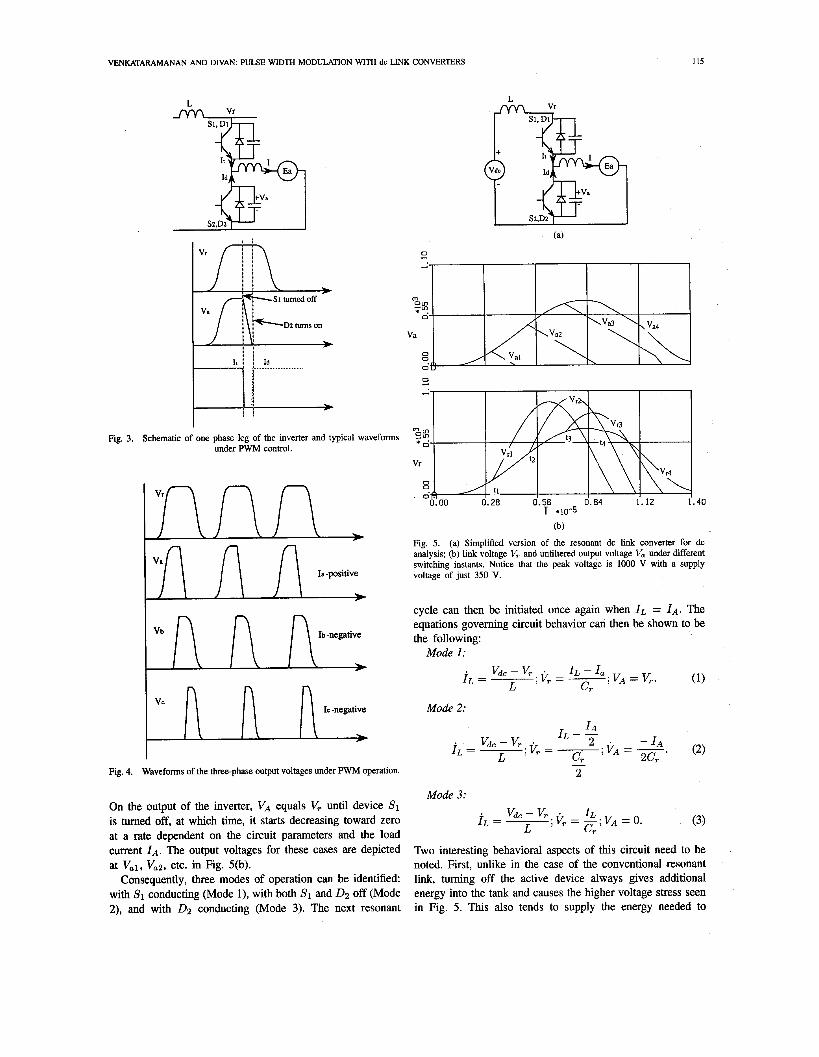
111. SIMPLIFIED ANALYSIS Although operation and control of the resonant link circuit
seems quite complex, it is possible to perform a simplified dc analysis that gives some insight into the obtainable control range as well as into the limitations of the scheme. The validity of this analysis is based on the assumption that the link frequency is much greater than the output frequency of the inverter. Fig. 5(a) shows one pole of the inverter, without the active clamp, operating with a positive load current IA. Fig. 5(b) shows the link and output voltage waveforms for various values of conduction time Ton for switch SI. At time t = 0, a resonant cycle is started between I, and the capacitor C,, which is across 5’2 (assuming S1 is conducting). If Sl is turned on part way through the cycle at instants t l , t 2 , etc., then trajectories denoted by V,I, V,Z etc. is followed by V,.
VENKATARAMANAN AND DIVAN PULSE WIDTH MODULATION WITH dc LINK CONVERTERS 115
L Vr
Fig. 3. Schematic of one phase leg of the inverter and typical waveforms under P W M control.
Ib -negative
>
Fig. 4. Waveforms of the three-phase output voltages under P W M operation.
On the output of the inverter, VA equals V, until device SI is tumed off, at which time, it starts decreasing toward zero at a rate dependent on the circuit parameters and the load current IA. The output voltages for these cases are depicted at Val, Vaz, etc. in Fig. 5(b).
Consequently, three modes of operation can be identified: with 5’1 conducting (Mode l), with both SI and D2 off (Mode 2), and with 0 2 conducting (Mode 3). The next resonant
T 110-5
Fig. 5. (a) Simplified version of the resonant dc link converter for dc analysis; (b) link voltage V, and unfiltered output voltage V, under different switching instants. Notice that the peak voltage is 1000 V with a supply voltage of just 350 V.
cycle can then be initiated once again when IL = IA. The equations governing circuit behavior can then be shown to be the following:
Mode I :
Mode 2:
- 2
Mode 3:
Two interesting behavioral aspects of this circuit need to be noted. First, unlike in the case of the conventional resonant link, tuming off the active device always gives additional energy into the tank and causes the higher voltage stress seen in Fig. 5. This also tends to supply the energy needed to
116 IEEE TRANSACTIONS ON INDUSTRY APPLICATIONS, VOL. 29, NO. 1, JANUARYFEBRUARY 1993
, Clamp Current losses incurred. These constraints apply in the steady state and are in addition to the absolute maximum limits on Ton described earlier.
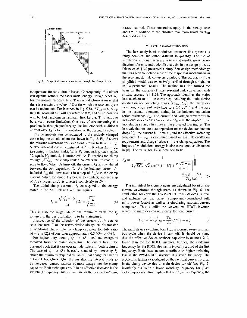
Fig. 6. Simplified current waveforms through the clamp circuit.
compensate for tank circuit losses. Consequently, this circuit can operate without the extra initial energy storage necessary for the normal resonant link. The second observation is that there is a maximum value of Ton for which the resonant cycle can be maintained. For instance, in Fig. 5(b), if Ton = t 4 > t 3 , then the resonant bus will not return to 0 V, and bus oscillation will be lost resulting in resonant link failure. This tends to be a very severe limitation. One way of circumventing this problem is through precharging the inductor with additional current over IA before the initiation of the resonant cycle.
The dc analysis can be extended to the actively clamped case using the circuit schematic shown in Fig. 3. Fig. 6 shows the relevant waveforms for conditions similar to those in Fig. 5. The resonant cycle is initiated at t = 0 when IL = IA (assuming a lossless tank). With SI conducting, once again, V, equals VA until SI is turned off. As V, reaches the clamp voltage (KVd,), the clamp switch conducts the current 1, is seen to flow. When SI turns off, the current IA is now shared between the two capacitors C,. As the inductor current IC included IA, this now results in a step of I A / ~ in the clamp current. When the diode D2 begins to conduct, another step of I*/2 occurs as IA is diverted completely to D2.
The initial clamp current -Ip correspond to the energy stored in the LC tank at t = 0 and equals
(4)
This is also the magnitude of the minimum value for I; required if the bus oscillation is to be maintained.
Irrespective of the direction of the current I,, it can be seen that turnoff of the active device always entails transfer of additional charge into the clamp capacitor for duty ratio ( d = Ton/T,) of less than approximately 0.5 (Q- > Q t ) .
For higher duty factors, Q+ > Q-, and net charge is removed from the clamp capacitor. The circuit has to be designed such that it can operate indefinitely in both regimes. The case of &- > Q+ is easily handled by increasing I; above the minimum required values so that charge balance is obtained. For Q- < Q+, the bus shorting interval needs to be increased, caused transfer of more charge into the clamp capacitor. Both techniques result in an effective decrease in the switching frequency, and an increase in the device switching
IV. Loss CHARACTERIZATION The loss analysis of modulated resonant link systems is
fairly complex and rather difficult to quantify. The use of simulation, although accurate in terms of results, gives no in- dication of trends and tradeoffs that exist in the design process. Divan et aZ. [12] presented a simplified design methodology that was seen to include most of the major loss mechanisms in the resonant dc link converter topology. The accuracy of the simplified model was extensively verified through simulation and experimental results. The method has also formed the basis for the analysis of other resonant link converters, with similar success [SI, [13]. The approach identifies the major loss mechanisms in the converter, including the main device conduction and switching losses (P,,, P,,), the clamp de- vice conduction and switching loss (P,,, P,,) and the loss in the resonant elements, mainly in the inductor equivalent series resistance PL. The current and voltage waveforms in individual devices are considered along with the impact of the modulation strategy to arrive at the projected loss figures. The loss calculations are also dependent on the device conduction drops VD, the current fall time t f , and the effective switching frequency Fs. Fs is calculated based on the link oscillation requirement and charge balance in the clamp capacitor. The impact of modulation strategy is also considered as discussed in [SI. The value for Fs is obtained to be
1
h cos-'(l- K ) + -
Fs =
The individual loss components are calculated based on the current waveforms through them, as shown in Fig. 6. The conduction loss for the PWM-RDCL main devices is Pcm and includes the load current component (considered with unity power factor) as well as a circulating resonant current component. This is unlike the conventional RDCL inverter, where the main devices only carry the load current:
1 I , + 2JZpTq 4 [
P,, = -v, 7r
The main device switching loss P,, is incurred every resonant bus cycle when the device is turn off. It should be noted that the effective device snubber capacitor is at most 2.C, lower than for the RDCL inverter. Further, the switching frequency for the RDCL devices is typically a third of the link frequency. Both these factors contribute to higher switching loss in the PWM-RDCL inverter at a given frequency. The problem is further exacerbated by the fact that current reversal in the clamp device due to main device turnoff (see Fig. 5 ) invariably results in a lower switching frequency for given LC components. This implies that for a given frequency, the
VENKATARAMANAN AND DIVAN: PULSE WIDTH MODULATION WITH dc LINK CONVERTERS
:$--
1 --
~
117
\ ~
Switching Loss :, Total
Loss Conduction Lo3---,," ......... .....-. ....... ............ ~.~ ..__. i.;: .............. ..................... ...--- - - ~
........... ESR Loss
capacitance would typically be smaller for the PWM-RDCL inverter as opposed to the conventional RDCL inverter, giving even higher switching loss. An approximate value for Psm can be shown to be
(7)
Similarly, the clamp device conduction loss and clamp device switching loss can be calculated to be
2(K - 1)
. [ ' d c T 31, (8) + -1 7r
L -I
(9)
The loss in the inductor ESR can be calculated by noting that the effective load dc current and the resonant current both flow through it. The loss PL is then found to be
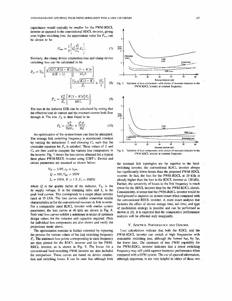
An optimization of the system losses can then be attempted. The average link switching frequency is maintained constant by varying the inductance L and choosing C, such that the constraint equation for F, is satisfied. These values of L and C,. are then used to compute the various loss components in the inverter. Fig. 7 shows the loss curves obtained for a typical three phase PWM-RDCL inverter using IGBT's. Device and circuit parameters are assumed as shown below:
VD = 3.OV,tf = ips, Q 100, v d c = 350V I, = 100A, K = 1.5, F, = 4OkHz
where Q is the quality factor of the inductor, v d c is the dc supply voltage, K is the clamping ratio, and I , is the peak load current. This corresponds to a single-phase inverter rated at 15 kVA. The loss curves exhibit somewhat similar characteristics as for the conventional resonant dc link inverter. For a comparably rated RDCL inverter with similar system parameters, the loss curves at 40 kHz are shown in Fig. 8. Both total loss curves exhibit a minimum in terms of optimum design values for the inductor and capacitor required. Plots for individual loss components are also shown and verify the projections made above.
The optimization exercise is further extended by repeating the process for various values of the link switching frequency F,. The minimum loss points corresponding to each frequency are then plotted for the RDCL inverter and for the PWM- RDCL inverter, as is shown in Fig. 9. The losses for a conventional hard-switching PWM inverter are also included for comparison. These curves are based on device conduc- tion and switching losses. It can be seen that although both
S
I > 10 20 30 40 50 60
Resonant Inductor (m Fig. 7. Variation of loss components with choice of resonant inductor in the
PWM RDCL inverter at constant frequency.
I \ ESRLoss -
Conduction .... .--. =----.----A .................................. + ..... swi%vi!!2gL.o~~~ ....._
I > 10 20 30 40 50 60
Resonant Inductor (UH) Fig. 8. Variation of loss components with choice of resonant inductor in the
PWM RDCL inverter at constant frequency.
the resonant link topologies are far superior to the hard- switching inverter, the conventional RDCL inverter always has significantly lower losses than the proposed PWM-RDCL inverter. In fact, the loss for the PWM-RDCL at 10 kHz is already higher than the loss in the RDCL inverter at 120 kHz. Further, the sensitivity of losses to the link frequency is much lower for the RDCL inverter than for the PWM-RDCL circuit. Consequently, it seems that the PWM-RDCL inverter would be hard pressed to improve on system losses when compared with the conventional RDCL inverter. A more exact analysis that includes the effect of device storage time, tail time, and type of modulation strategy is possible and can be performed as shown in [SI. It is expected that the comparative performance analysis will be affected only marginally.
V. SPECTRAL PERFORMANCE AND CONTROL Loss calculations indicate that both the RDCL and the
PWM-RDCL inverter can switch at high frequencies with reasonable switching loss, although the former has, by far, the lower loss. The existence of true PWM capability for the PWM-RDCL inverter indicates that a lower switching frequency may still yield superior harmonic performance when compared with a DPM system. The use of spectral information, although important, is not very helpful in either of these two
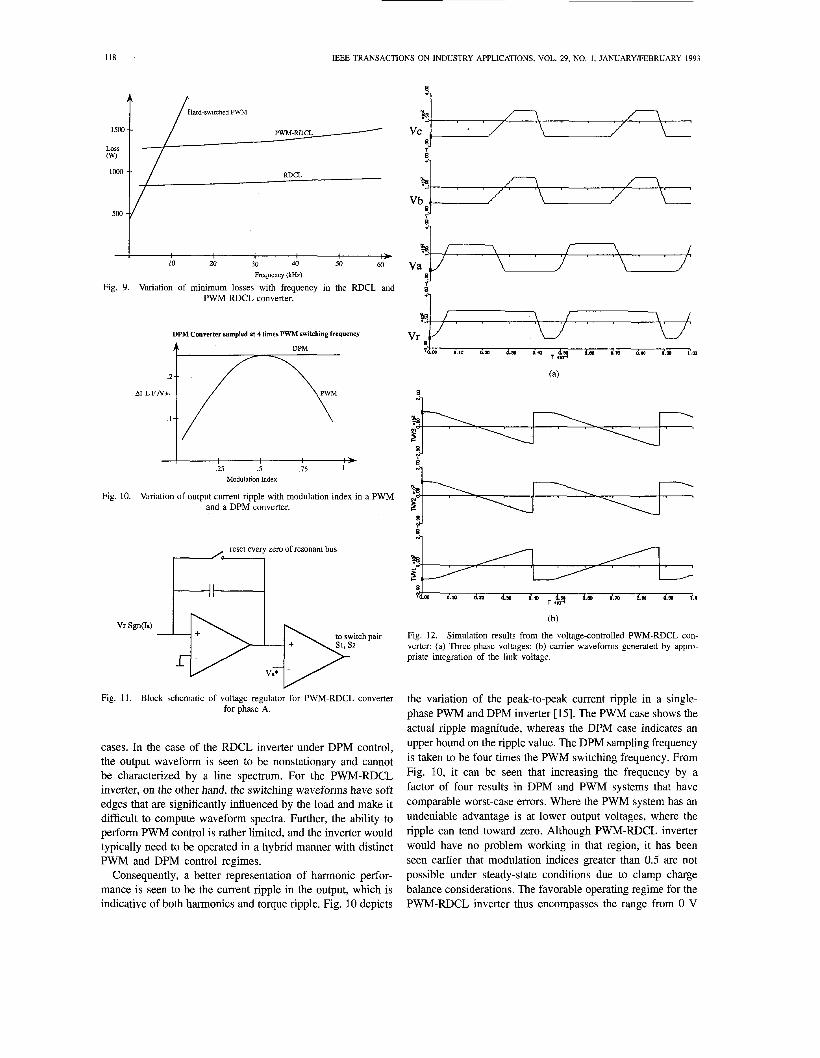
Hard-switched PWM t / IEEE TRANSACTIONS ON INDUSTRY APPLICATIONS, VOL. 29, NO. 1, JANUARYFEBRUARY 1993
RDCL
loo0 t / 10 20 30 40 50 60
Frequency (Hz)
Fig. 9. Variation of minimum losses with frequency in the RDCL and PWM-RDCL converter.
DPM Converter sampled at 4 times PWM switching frequency
A DPM
AI L F N &
I > .25 5 .75 1
Modulation Index
Fig. 10. Variation of output current ripple with modulation index in a PWM and a DPM converter.
reset every zero of resonant bus
17
Fig. 11. Block schematic of voltage regulator for PWM-RDCL converter for phase A.
cases. In the case of the RDCL inverter under DPM control, the output waveform is seen to be nonstationary and cannot be characterized by a line spectrum. For the PWM-RDCL inverter, on the other hand, the switching waveforms have soft edges that are significantly influenced by the load and make it difficult to compute waveform spectra. Further, the ability to perform PWM control is rather limited, and the inverter would typically need to be operated in a hybrid manner with distinct PWM and DPM control regimes.
Consequently, a better representation of harmonic perfor- mance is seen to be the current ripple in the output, which is indicative of both harmonics and torque ripple. Fig. 10 depicts
2,
!,
8 d.ro dm dm d.r, T $ ~ d.m dm dm i s 0 i . 0
(b) Fig. 12. Simulation results from the voltage-controlled PWM-RDCL con- verter: (a) Three-phase voltages; (b) carrier waveforms generated by appro- priate integration of the link voltage.
the variation of the peak-to-peak current ripple in a single- phase PWM and DPM inverter [15]. The PWM case shows the actual ripple magnitude, whereas the DPM case indicates an upper bound on the ripple value. The DPM sampling frequency is taken to be four times the PWM switching frequency. From Fig. 10, it can be seen that increasing the frequency by a factor of four results in DPM and PWM systems that have comparable worst-case errors. Where the PWM system has an undeniable advantage is at lower output voltages, where the ripple can tend toward zero. Although PWM-RDCL inverter would have no problem working in that region, it has been seen earlier that modulation indices greater than 0.5 are not possible under steady-state conditions due to clamp charge balance considerations. The favorable operating regime for the PWM-RDCL inverter thus encompasses the range from 0 V
119
~ ~~
Fig. 13. Traces of resonant link voltage and modulated output voltage from an experimental PWM-RDCL converter: voltage 100 V/div, time 20 ps/div.
to an average duty cycle of less than 0.5, above which a DPM strategy would need to be adopted.
The PWM-RDCL inverter can be controlled in a manner akin to the sinusoidal PWM method. A block diagram of the proposed controller is shown in Fig. 11. The carrier for modulating the link voltage is derived by integrating the resonant link voltage. The integrator is reset at every zero crossing of the bus voltage. The slope of the carrier could be positive or negative, determined by the polarity of the phase current at the zero crossing of the bus. This allows the carrier wave to be inverted based on which device is initially conducting. The turnoff instant for the conducting device is then determined by the intersection of the carrier and control signal. Subcycle turnoff of the device is only permitted within limiting bounds, beyond which the entire resonant pulse appears on the phase output. The error can obviously be carried over from one cycle to the next to further improve performance. Fig. 12 shows simulation wave- forms for the PWM-RDCL inverter operating under voltage control. Current control of the PWM-RDCL inverter is also possible but will not be discussed here in the interest of brevity.
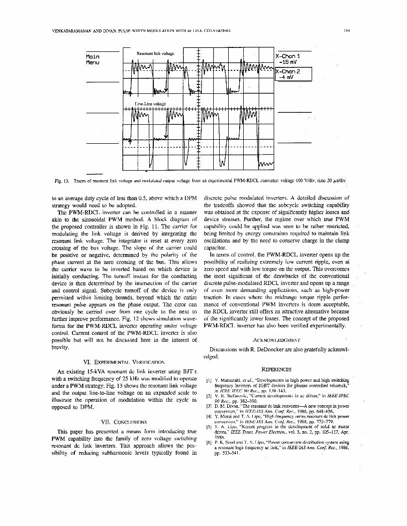
VI. EXPERIMENTAL VERIFICATION An existing 15-kVA resonant dc link inverter using BJT’s
with a switching frequency of 25 kHz was modified to operate under a PWM strategy. Fig. 13 shows the resonant link voltage and the output line-to-line voltage on an expanded scale to illustrate the operation of modulation within the cycle as opposed to DPM.
VII. CONCLUSIONS This paper has presented a means form introducing true
PWM capability into the family of zero voltage switching resonant dc link inverters. This approach allows the pos- sibility of reducing subharmonic levels typically found in
discrete pulse modulated inverters. A detailed discussion of the tradeoffs showed that the subcycle switching capability was obtained at the expense of significantly higher losses and device stresses. Further, the regime over which true PWM capability could be applied was seen to be rather restricted, being limited by energy constraints required to maintain link oscillations and by the need to conserve charge in the clamp capacitor.
In terms of control, the PWM-RDCL inverter opens up the possibility of realizing extremely low current ripple, even at zero speed and with low torque on the output. This overcomes the most significant of the drawbacks of the conventional discrete pulse-modulated RDCL inverter and opens up a range of even more demanding applications, such as high-power traction. In cases where the midrange torque ripple perfor- mance of conventional PWM inverters is deem acceptable, the RDCL inverter still offers an attractive alternative because of the significantly lower losses. The concept of the proposed PWM-RDCL inverter has also been verified experimentally.
ACKNOWLEDGMENT Discussions with R. DeDoncker are also gratefully acknowl-
edged.
REFERENCES
Y. Matsuzaki, et al., “Developments in high power and high switching frequency inverters of IGBT devices for plasma controlled tokomak,” in IEEE IPEC 90 Rec., pp. 139-143. V. R. Stefanovic, “Current developments in ac drives,” in IEEE-IPEC 90 Rec., pp. 382-390. D. M. Divan, “The resonant dc link converter-A new concept in power conversion,” in IEEE-IAS Ann. Con$ Rec., 1986, pp. 648-656. Y. Murai and T. A. Lipo, “High frequency series resonant dc link power conversion,” in IEEE-IAS Ann. Con$ Rec., 1988, pp. 772-779. T. A. Lipo, “Recent progress in the development of solid ac motor drives,” IEEE Trans. Power Electron., vol. 3, no. 2, pp. 105-117, Apr. 1988. P. K. Sood and T. A. Lipo, “Power conversion distribution system using a resonant high frequency ac link,” in IEEE-IASAnn. Con$ Rec., 1986, pp. 533-541.
120 IEEE TRANSACTIONS ON INDUSTRY APPLICATIONS, VOL. 29, NO. 1, JANUARYFEBRUARY 1993
[7] D. I! Divan and G. L. Skibinski, “Zero switching loss inverters for high power applications,” in IEEE-IAS Ann. Con$ Rec., 1987, pp. 627-634.
[8] A. Mertens and D. M. Divan, “A high frequency resonant dc link converter using IGBT’s,” in IEEE-IPEC 90 Rec., pp. 152-260.
[9] L. Malesani and D. M. Divan, “A synchronized resonant dc link converter for soft-switched PWM,” in IEEE-IAS Ann. Con$ Rec., 1989, p p . 1037-1044.
[IO] R. De Doncker and G. Venkataramanan, “A new single phase ac to dc zero voltage soft-switching converter,” in IEEE PESC 90 Rec., pp. 206212.
[ I l l G. L. Skibinski and D. M. Divan, “Characterisation of GTO’s for soft switching applications,” in IEEE-IAS Ann. Con$ Rec., 1987, pp.
[12] D. M. Divan, G. Venkataramanan, and R. W. DeDoncker, “Design methodologies of soft switched inverters,” in IEEE-IAS Ann. Con$ Rec., 1987, p p . 626-639.
[13] P. Caldeira and T. A. Lipo, “Design and control of a series resonant dc link converter,” in IEEE IPEC 90 Rec., pp. 397-404.
[14] G. Venkataramanan, D. M. Divan, L. Malesani, and V. Toigo, “Control strategies for synchronized resonant link inverters,” in IEEE IPEC 90 Rec., pp. 338-345.
638-646.
Giri Venkataramanan received the B.E. degree from the Government College of Technology, Coim- batore, India, the M.S. degree from the California Institute of Technology, Pasadena, and the Ph.D. de- gree from the University of Wisconsin, Madison, in 1986, 1987, and 1992, respectively, all in electrical engineering.
Currently, he is an Assistant Professor of Electri- cal Engineering at Montana State University, Boze- man. His research interests are in modeling, design, and control of power conversion systems.
Deepakraj M. Divan (SM’91) received the B.Tech degree in electrical engineering from the Indian Institute of Technology, Kanpur, India in 1975. He also received the M.Sc. and Ph.D. degrees in electncal engineering from the University of Calgary, Calgary, Canada. He worked for two years as a Development Engineer with Philips India Ltd. After finishmg the Masters program in 1979, he started his own concem in Pune, India, providing product development and manufacturing services in the power electronics and instrumentation areas. In
1983, he joined the Department of Electncal Engineering at the University of Alberta as an Assistant Professor. Since 1985, he has been with the Department of Electncal and Computer Engineenng at the University of Wisconsin, Madison, where he is presently a Professor. He is also an Associate Director of the Wisconsin Electric Machine and Power Electromcs Consortium, (WEMPEC), which is a group of approximately 45 industrial sponsors supporting research in the area of power electronics and machines. His primary areas of interest are in power electronic converter circuits and control techniques. He has over 40 papers in the area as well as many patents.
Dr. Divan has been a recipient of the Killam Scholarshp during his Ph.D program and has also won various prize papers including the IEEE- IAS Best Paper Award for 1988-89, prize papers for the Industrial Drives Committee in 1989 and 1991, the Industrial Power Converter Committee in 1983, 1989, and 1991, and the Power Semiconductor Committee in 1990. He is a consultant for vanous organizations including the Electric Power Research Institute, Oakridge National Laboratory, and is also workmg with several industries. He has been the Program Chairman for the 1988 and 1989 Industrial Power Converter Committee of the IEEE-IAS, Transactions Review Chair for the committee in 1990 and 1991, and is presently Vice Chairman of the Committee. He was Technical Program Chamnan for PESC 91 and a Treasurer for PESC 89. He was Chairman of the Education Committee in the IEEE Power Electronics Society dunng 1990 and 1991 and is presently an elected Member at Large in the society’s Administrative C o m t t e e . He is a member of the Research and Development Comrmttee of the Power Sources Manufacturers Association and has been a member of the National Committee on Power Electronics.