Embed Size (px)
Citation preview
C
SMALL-SIGNAL CHARACTERISTICS OF DIODE- STABILIZED LINEAR INTEGRATED DEVICES"
Edward S. Yang Department of Electr ical Engineering
Columbia University, New York, N. Y. 10027
GPO PRICE $
CFSTI PRICE(S) $ I
Hard copy (HC) q-. & 5
Microfiche (M F) , Ls--
ff 663 July 66
y e 8 - 1 7 O 0 9 (THRU) (ACCESSION NUMBER)
* This work was supported by the NSF Research Grant GK-1550, and the NASA Grant NGR 33-008-090.
https://ntrs.nasa.gov/search.jsp?R=19680007540 2018-05-22T02:15:17+00:00Z
’ ABSTRACT
Small-signal charac te r i s t ics and frequency response of diode-
The s tabi l ized linear integmted devices ( c i r c u i t s ) are examined.
bu i l t - i n feedback property i s explained,
cuit provides low input impedance, high output impedance and small
internal feedbck. The frequency response of the c i r c u i t with the
bias-diode i s superior% t o t h a t without the bias-diode.
gain o€ the ctvci1+? can be controlled by appropridte design of
active elements or passive elements.
discrete components agree with the analysis.
3t is found that the cir-
The current
The experimental r e s u l t s using
.I. INTRODUCTION
I n the design of l inear integrated c i r cu i t s , one of the basic
problems i s the biasing of a common-emitter (CE) stage. The con-
ventional biasing techniques used in discrete c i r c u i t design a re not
pract ical because of the requirement of a large emitter bypass capa-
c i t o r , I n order t o overcome t h i s d i f f icu l ty , Widlar has developed a 1 method using a diode-connected t rans is tor t o s t ab i l i ze a CE stage.
A modified circuit (or device) i s reported by Davis and Lin where a
compound diode-transistor structure i s used f o r temperature compensa-
tion.* In these papers, the s tabi l izat ion aspect of the circuits i s
emphasized, but other characterist ics of the circuits have not been
treated. Since these c i rcu i t s a r e designed for l inear applications,
one should consider both the s tab i l iza t ion properties and the small-
signal characterist ics such as input impedance, output impedance,
in te rna l feedback factor and the frequency response of the circuit.
The purpose of t h i s work is t o investigate the small-signal
character is t ics of the diode-stabilized CX c i r c u i t f o r l inear
integrated-circuit applications. It i s found that the c i r c u i t is a
very good current amplifier with low input impedance, high output Im-
pedance and low internal feedback factor. The frequency response of
the circuit with t h e bias-diode is much be t te r than t h a t without the
bias-diode. These improvements on device charac te r i s t ics a re obtained
- 2 - !
however with a sacr i f ice of the Current gain, The experimental re -
s u l t s using d iscre te components agree with the analysis,
XI, THE FEEDBACK CONCEPT
The small-s5wl behavior of the diode-stabilized c i r c u i t does
not seem t o be predictable a t the f irst glance because of t he uncon-
ventional form of the diode-transistor connection,
however, t o show t h a t the c i r cu i t i s actually a form of the current-
shunt feedback amplifier.
can predict the small-signal character is t ics of the c i r c u i t .
method of analysts m y p??,l)vide be t te r physical insight of the circuit
operation and enable the designer t o mke fur ther modification.
I It i s possible,
Based on the simple feedback concept one
This
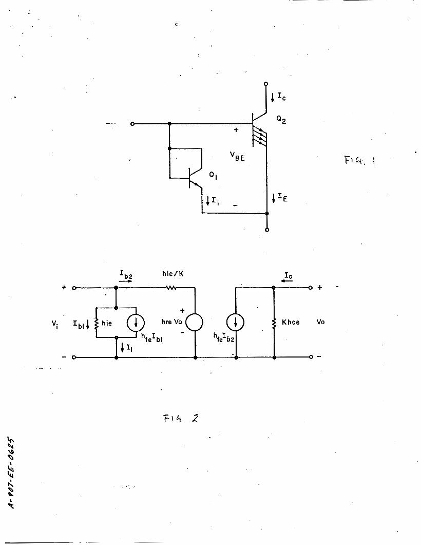
The circuit of Davis and Lin (Fig. 1) may be treated as a nega-
t i v e feedback c i r c u i t where the output current i s sampled and is f ed
back t o the input i n shunt connection,
has t o be the same for the t ransis tor 92 and the diode-connected
t rans is tor Ql.
IE of % and, thus, proportional t o IC of Qz. taken as the feedback current and Xc of 42 can be taken as t h e output
Physically, the voltage VBE
A s a result, the diode current Il is proportional t o
The current I1 can be
current.
ren t gain of the circui t .3 The s tab i l iza t ion is achieved with a
This current-shunt feedback connection s tab i l izes the cur-
i sacr i f ice of cu r ren t gain. Furthernore, the diode-biased connection
should reduce the input impedance and should increase the output i m -
I pedance .
0 1 - I - 3 -
I
Natheinatital3.y, the feedback sicpal I1 is related t o t he output
current IC by the following express ion :
where K is the ratio of the transistoil emitter area to the diode
emitter area and Ic0 is assumed negligible,
feedback factor is
Therefore, the dc
By making use of the general forau la of a feedback amplifier, the
overal l current-gain AIf otith feedback is
is used. The foregoiig eqmtion is ident ica l t o hFE where AI =
Eq. ( 4 ) of Davis a d Lin. The variation of the current gain, due to
t h e change of tcmpcrature or operating pint, is greatly: reduced be-
cause of the feedbzck action.
- 4 -
III. THE LOI.?-FREQUENCY SMALL-SIGNAL PAPWETERS
I n the small-signal analysis, t he following assumptions arc made:
(1) Q2 is made up of K t rans is tors connected i n para l le l
(2) all t rans is tors are ident ical
( 3 ) the h-pammcters of each t rans is tor a r e hie, hre, hfe
and hoe.
l/hoe i s large compared t o hie, and hre of Ql is negligible. (4)
F'rom these assumptions, the h-parameters of Qz become hie/K, hre,
and K hoe. Tne equations describing the basic amplifier 42 a re , hfe therefore,
,
. If the feedback concept is used,
amplifier and Ql as t he feedback network.
l e n t c i r c u i t i s shovm i n Fig. 2.
hf and ho are found by making use of Fig. 2:
m y be considered as the basic
The small-signal equiva-
The overa l l h-parameters hi, hr,
. A. Input Impedance (hi): The input impedance of the c i r cu i t i s
the para l le l combination of the impedances looking into the diode
Ql (hid) and the base of the t rans is tor % (hit).
a're given by:
These impedances
CL . .
h i t =
Therefore, t he input impedance becomes
- hie - hid hit - hi -. hid + hit 1 + X + hfe
Alternat ively, the input impedance can be obtained by using the
feedback method, Thus,
where
pedance can be made very small by choosing a large hfeo
$ @ = (I + hfe)/K hfe and Zi = hie/K are used. The input i m - i .
B. Forward Current-Transfer Ratio (hf): The expression for
the forward current-transfer r a t i o can be derived by using the feed-
back method.
- hfe hf - 1 + K + hfe
J . .
I
0 - 6 -
C. Voltage Feedback'Ratio (hr): The voltage feedback r a t i o can
be calculated by solving Eq. (4 ) and making use of the re la t ion of
vi/Ib2 = - hid. The resultant expression is
D. Output Impedance (hJ: Equation ( 5 ) may be rewrit ten as
'b2 vO = hfe q- + hoe I,
Since Ib2 = - 11, one obtains
'b2 I1 + hfe IO IO I( hfe - = - - = -
By subst i tut ing Eq. (13) into Eq. (12), t h e following expression
i s obtained:
Io - hoe h o = j ; ; - 1 + K + hie
T h i s resu l t can also be obtained by using the negative feedback
concept.
With the foregoing results, expressions including the effects
of the source and load impedance can be obtained easily.
i
- 7 - .
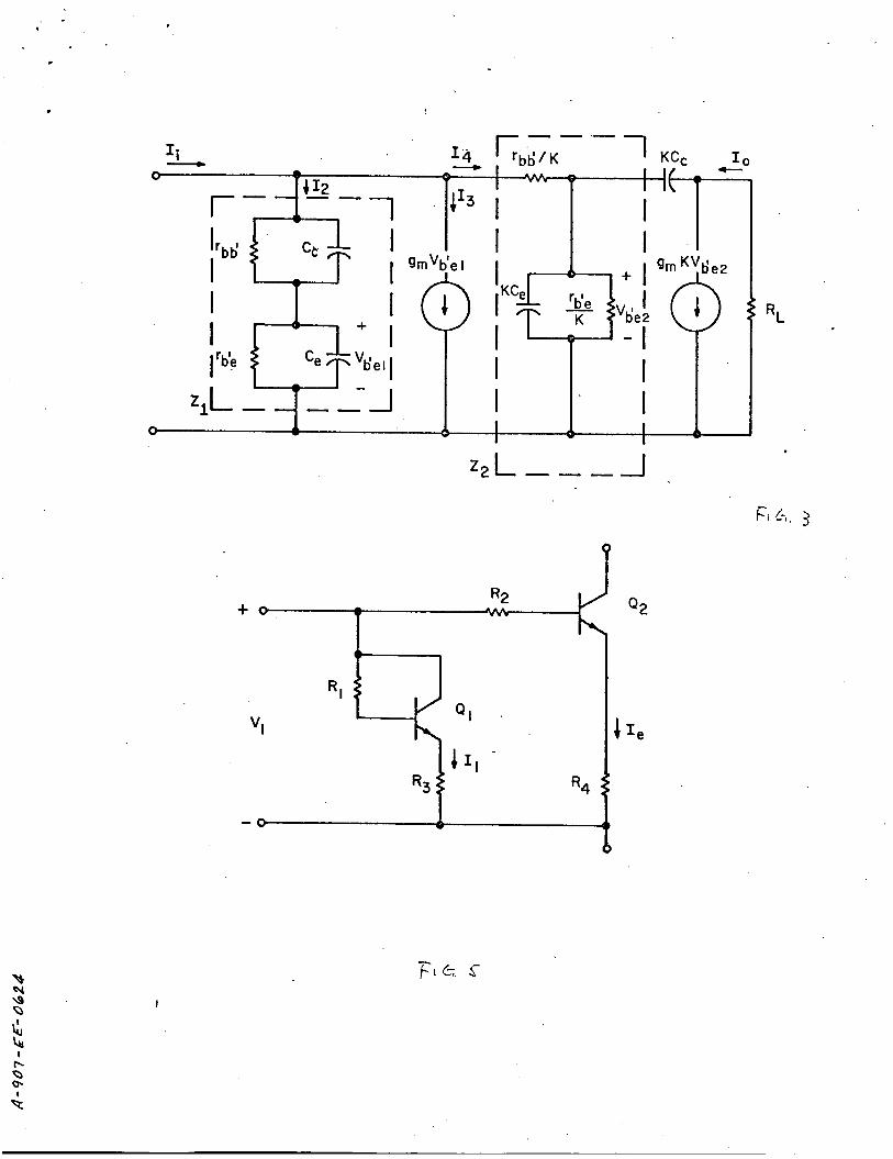
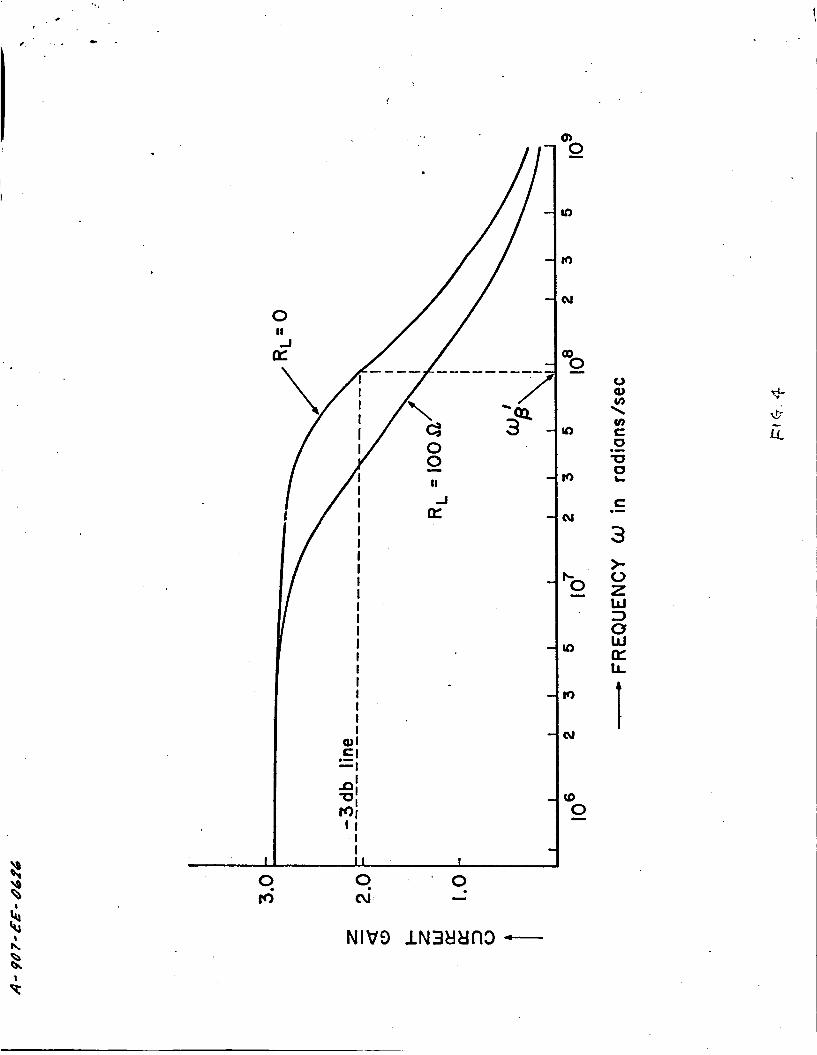
xv. FREQ UENCY RESPONSE
The frequency response of the functional block is of primary
importance since the functional block is the basic component of a
l inear amplifier. An equivalent c i r cu i t using the hybrid-rr model
(Fig. 3) m y be used f o r the calculation of the 3-db frequency of
the short-circuited current gain,
one may expect a higher 3-db frequency for the s tabi l ized c i r cu i t .
From the negative feedback concept,
To simplify the derivation, it is assumed t h a t C, >> c,, % = 0 .
Furthermore, the following equivalent representations are used:
The following equations can be obtained from Fig. 3:
li = I + I3 I- x 4 - 2
12Zl = 14Z*
- 8 - 0
By solving Eqs . (17) through (20) ,- one obtains
The r a t i o Zl/Z2 turns out t o be I( i f the e f f ec t of C, is
negligible. As a r e s u l t , Eq. (21) becomes
where f
diode.
i s the cutoff frecpency of the CE stage without the biasing B The cutoff frequency with the biasing diode becomes
A bet te r frequency response is realized €or the stabi l ized CE stage.
This result i s not obvious if one does not t r e a t the c i r c u i t from
the feedback vfetvpoint . If % ?c 0, the effect of Cc cannot be ignored. By using
Miller’s theorem t o account f o r Cc, the fo l lowbg expression f o r the
current gain can be obtained:
- 9 -
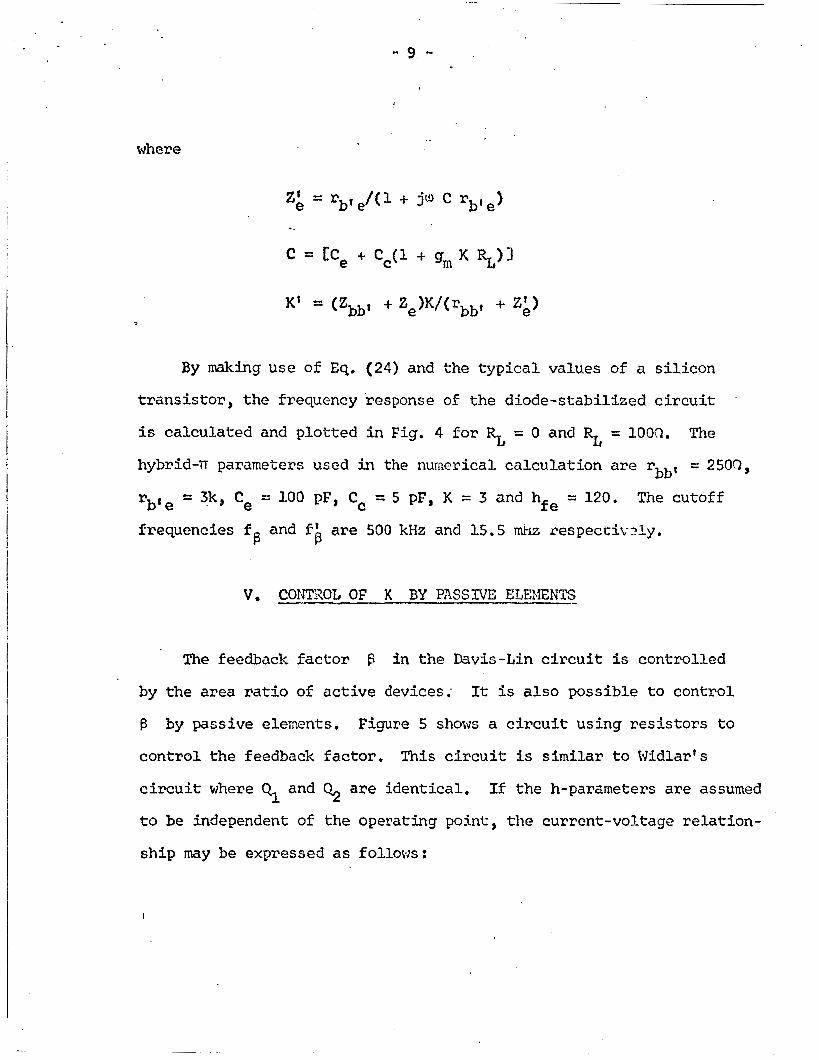
where
By making use of Eq. (24) and the typ ica l values of n si l icon
t rans is tor , the frequency response of the diode-stabilized c i r cu i t
is calculated and plotted in Fig . 4 fo r % = 0 and RL = IOOQ. The
hybrid-rr parameters used in the numerical calculation are rbb, = 250c),
rb8 e frequencfes f
= 3k, Ce = 100 pF, C, = 5 pF, K = 3 and hfe = 120, The cutoff
and f1 are 500 kHz and 15.5 mtiz respectiv?ly, B P
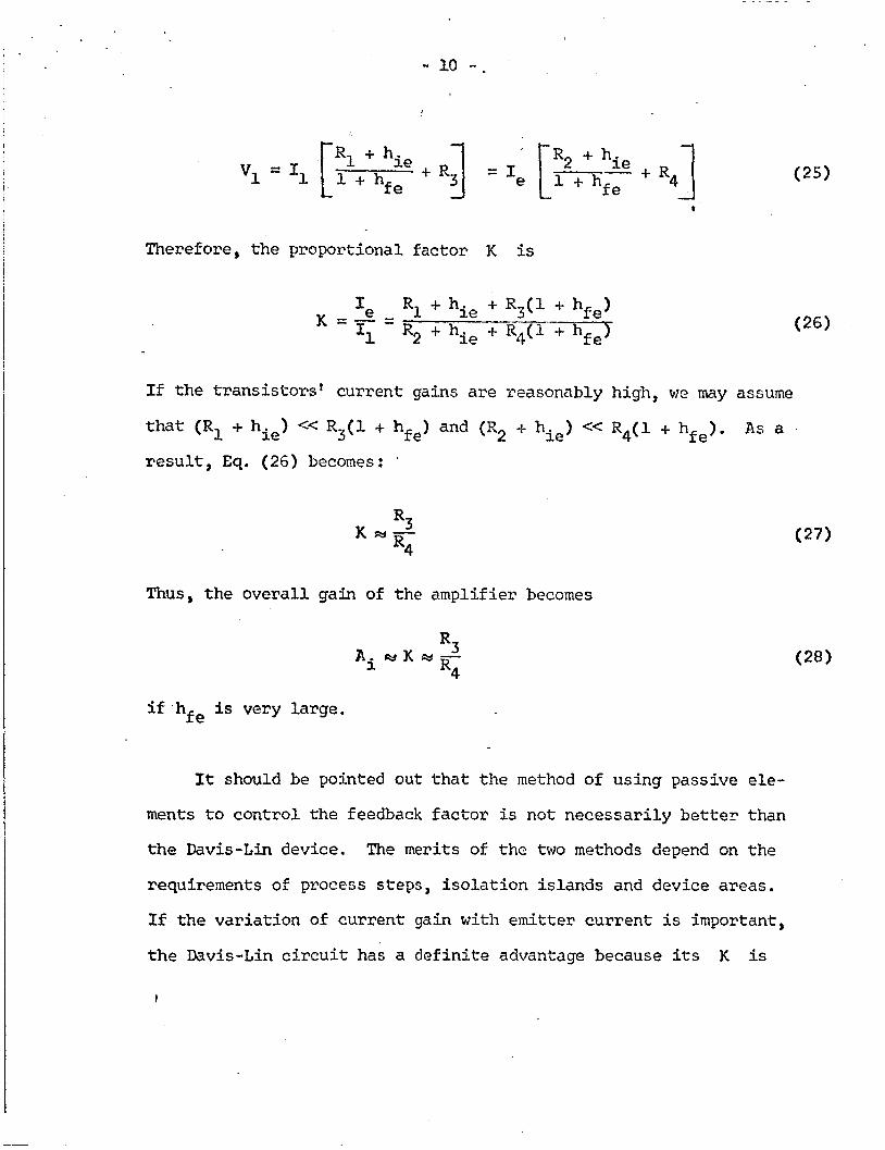
v. CONTXOL OF K BY PASSIVE ELEMENTS
The feedback factor €3 i n the Davis-Lin c i r c u i t i s controlled
by the area r a t i o of active devices;
6 by passive elements,
control the feedback factor.
c i r c u i t where Q and Q2 are identical . If the h-parameters a re assumed
t o be independent of the operating point, the current-voltage relation-
sh ip may be expressed as follows:
It I s also possible t o control
Figure 5 shows a c i r c u i t u s i n g res i s tors t o
This c i r c u i t i s similar t o Widlar's
1
I
" 10 - _ ,
Therefore, t he proportional factor K i s
If the t rans is tors t current gains are reasonably high, we may assume
t h a t (R1 j. hie) << R3(l + hfe) and (R2 $- hie) << R4(l + hfe).
r e s u l t , Eq. (26) becomes: .
As a
R3 R4
K S j -
Thus, the overal l gain of the amplifier becomes
R3 R4
A . w K w - 1
if 'hfe is very large.
It should be pointed out t h a t the method of using passive ele-
ments t o control the feedback facton? i s not necessarily better than
the Davis-Lin device. The m e r i t s of the two methods depend on the
requirements of process steps, i so l a t ion islands and device areas.
If the variation of current gain with emitter current i s important,
t h e Davis-Lin c i r c u i t has a def ini te advantage because i t s K is
I
independent of the' operating current,
emitter r e s i s to r s does not provide the
and the t ransis tor . Thus, hfel f hfe2
The c i r cu i t using different
same current for the diode
and K would not be a constant,
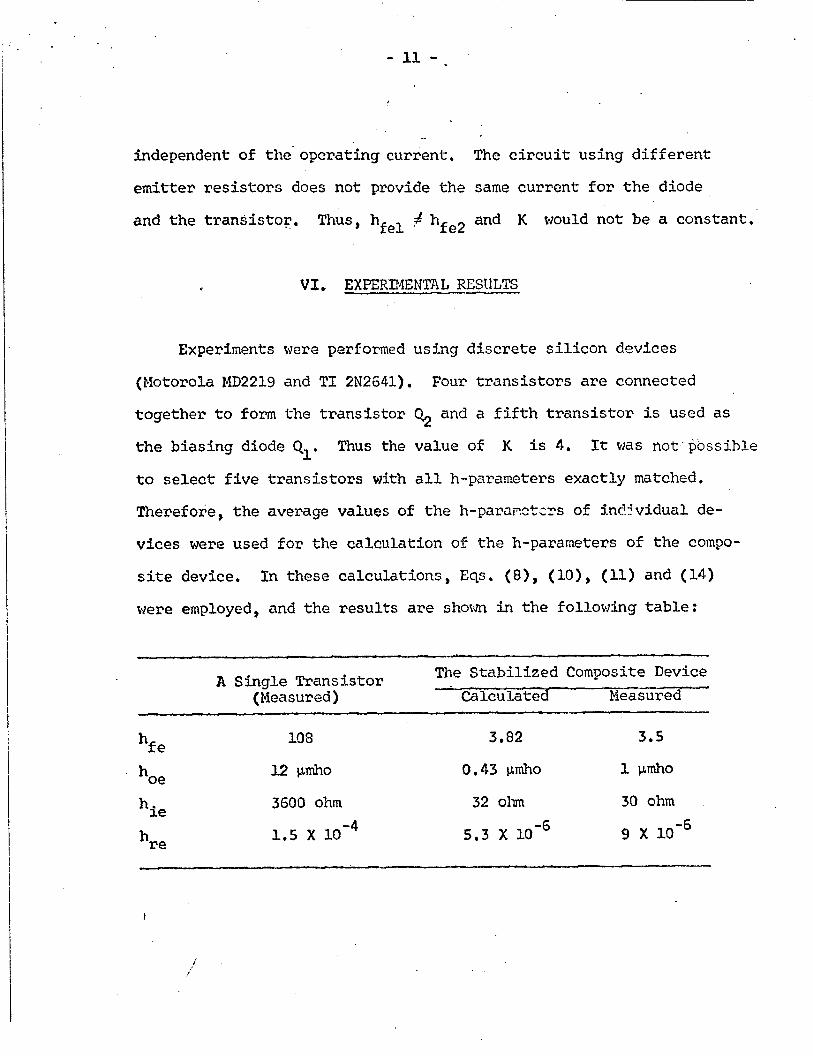
VI. EXPERIMENTAL REStlLTS
Experiments were perforned using discrete s i l i con devices
(Motorola MD2219 and T I 2N2641).
together t o fom the transfstor 42 and a f i f t h t rans is tor i s used as
the biasing diode Ql. Thus the value of K is 4. It was not possible
t o se lec t f i ve t rans is tors with all h-parameters exactly matched,
Tinerefore, the average values of the h-paramcters of inclfvidual de-
vices were used for the calculation of t he h-parameters of the compo-
s i te device.
were employed, and the resul ts are shown in the following table:
Four t rans is tors a re connected
In these calculations, Eqs. (8), (lo), (11) and (14)
The Stabilized Composite Device A Single Transistor (Measured) Calculated MeTsured
10s 3.82 3.5
l2 pmho 0.43 vmho 1 pmho
hf e
. hoe 3500 ohm hie 1.5 x
32 ohm 30 ohm
5.3 x 9 x
- 12 - I
4 1
The measured and calculated resuzts a re -c lose despi te the unmatched
parameters and the current-hogging e f k c t , In a device such a s the
Davis-Lin circuit , the correlation between the calculated and measured
r e su l t s should be better.
The frequency response of % and the composite circurt a = 3 ) was
measured.
ohm was used.
over 10 mHz.
theory and experiment was not possible when d iscre te devices were
used, because of the spread of hybrid-rr parameters, the ex t r ins ic
The cutoff frequency fo r 42 alone weis 350 kHz when RL = 100
The cutoff frequency fo r the composite c i r c u i t was
Unfortunately, quantitative comparison between the
elements and current hogging,
i n agreement w i V % t h e themy (Fig. 4) qualj-tativcly.
However, the experimental results a re
Further study
of the frequency response using the Davis-Lin device is desirable.
V I I . CONCLUSION
An analysis of the diode-stabilized l i n e a r integrated circuit
has been made based. on the simple ‘feedback concept. The small-signal
parameters were derived t o demonstrate the e f f e c t s of the diode con-
nected t rans is tor .
impedance, high output impedance and low i n t e r n a l feedback factor.
The cutoff freopancy of the diode-stabilized c i r c u i t i s approxirrately
It has been shcwn tha t t h e c i r c u i t has low input
-
i- 10 times the cutoff f rcquency of the CE stage without the
biasing diode. The advantages, however, are achieved with a sacr i f ice
- 13 - !
of the current gain.
ments could be used t o control the character is t ics of the c i r cu i t .
Thus, the external character is t ics of the c i r c u i t can be modified by
e i the r active or passive elements o r both,
s ignal analyses were confirmed by experiments using discrete components.
I n principle, the diode-stabilized CE stage is not be t t e r than
The feedback factor of the s tabi l ized c i r -
Finally, it was emonstrated tha, passive d e -
The r e su l t s of the small-
any feedback amplifier.
c u i t i s frequency dependent when s t ray elements (such as overlap-
diode capacitance) are taken into account,
complicated i f mismtched components are used.
cations, however, t h i s circuit is simpler than any other exis t ing
c-ir.cui.ts.
of integrated c i r cu i t s such as close matching and thermal coupling
of active and temperature sensit ive components.
The analysis is further
In practical appli-
Furtherrnoye, it takes advantage of the desirable features
i
REFERENCES
1.
2.
3.
4.
R. J, Widlar,’71Some Circuit Design Techniques for Linear
Integrated Circuitsl l , XEEE Trans, on Circui t Theory, vol.
CT-12, pp. 586-530, December 1965.
W. R. Davis and H . C. Lin, l1Compound Diode-Transistor Structure
for Temperature Compensationr1, h o c . IEEE, vol. 54, pp, 1201-1202,
September 1966.
J. Millman and C. C. Halkias, ltElectronic Devices and Circuits1?,
Ch, 17, New Yorlc:
C, R. Hoffman, “Temperature Sensi t ivi ty of Compound Diode-
I’ransistor Structure1f, Proc. IEEE, V G ~ . 5 5 , gp. 1233-1234,
July 1967
McGraw-Hill, 1967.
I
FIGURE CAk!IONS
Fig. 1 - The Davis-LLn Device
F i g , 2 - The Small-Signal Equivalent Circuit of Fig. 1
Fig. 3 - The Hybrid-rr Model
Fig. 4 - The Frequency Response of the Diddc-Stabilized Circuit
F i g . 5 - A Stabilized Circui t with Passive Elements
6
+ *be hie/K -
0 %A&
vi IT-$ I hre
fe bl
IT-$ I hre
fe bl
Khoe Vo
. . .
.
gmVb'e I Q RL
"I
I
0 tri
I I I
8j WI I 1
I I
0 cu'.


![a2 circuit elements-diode [相容模式]](https://img.pdfslide.us/doc/110x75/623347216d8a553e72022bb0/a2-circuit-elements-diode-.jpg)