Embed Size (px)
Citation preview

PRACTICAL # 08Diode Clamper Circuit.
By:Engr.Irshad Rahim Memon
OBJECTIVE Objective of this practical is to learn that
how a diode can clamp the signal.
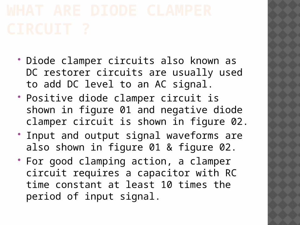
WHAT ARE DIODE CLAMPER CIRCUIT ?
Diode clamper circuits also known as DC restorer circuits are usually used to add DC level to an AC signal.
Positive diode clamper circuit is shown in figure 01 and negative diode clamper circuit is shown in figure 02.
Input and output signal waveforms are also shown in figure 01 & figure 02.
For good clamping action, a clamper circuit requires a capacitor with RC time constant at least 10 times the period of input signal.
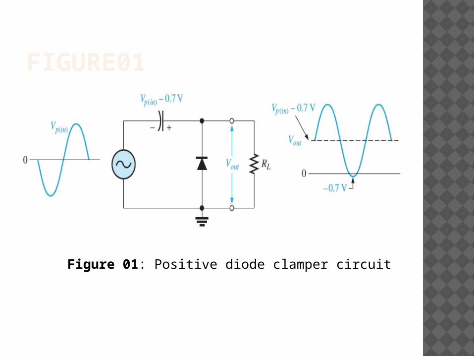
FIGURE01
Figure 01: Positive diode clamper circuit
DIODE CLAMPER CIRCUIT CONTINUED… Positive diode clamper circuit inserts a positive DC level
in the output waveform. When negative half cycle of input AC signal is provided
to positive diode clamper circuit, diode is forward biased and capacitor will be charged up to voltage level (Vin-0.7), because diode has to drop 0.7volts.
During when positive half cycle of input AC signal is provided to positive diode clamper circuit, diode is reverse biased and as capacitor is already charged up to voltage level (Vin-0.7)volts, now this capacitor will work as a battery of (Vin-0.7)volts, that’s why capacitor voltage is added with positive half cycle of AC input signal, furthermore this capacitor voltage will also be added with next negative half cycle of input AC signal. In result input AC signal is shifted upward by the magnitude of (Vin-0.7)volts.
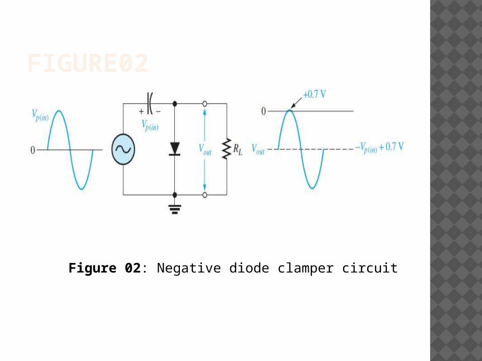
FIGURE02
Figure 02: Negative diode clamper circuit
DIODE CLAMPER CIRCUIT CONTINUED… Negative diode clamper circuit inserts a negative DC level
in the output waveform. When positive half cycle of input AC signal is provided to
negative diode clamper circuit, diode is forward biased and capacitor will be charged up to voltage level (Vin-0.7), because diode has to drop 0.7volts.
During when negative half cycle of input AC signal is provided to negative diode clamper circuit, diode is reverse biased and as capacitor is already charged up to voltage level (Vin-0.7)volts, now this capacitor will work as a battery of (-Vin+0.7)volts, that’s why capacitor voltage is added with negative half cycle of AC input signal, furthermore this capacitor voltage will also be added with next positive half cycle of input AC signal. In result input AC signal is shifted downward by the magnitude of (Vin-0.7)volts.
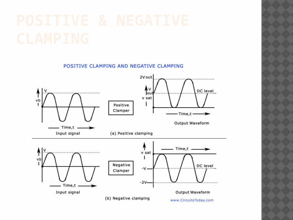
POSITIVE & NEGATIVE CLAMPING
DESCRIPTION CONTINUED.. A clamp circuit adds the positive or negative dc
component to the input signal so as to push it either on the positive side, as illustrated in figure (a) or on the negative side, as illustrated in figure (b).
The circuit will be called a positive clamper , when the signal is pushed upward by the circuit. When the signal moves upward, as shown in figure (a), the negative peak of the signal coincides with the zero level.
The circuit will be called a negative clamper, when the signal is pushed downward by the circuit. When the signal is pushed on the negative side, as shown in figure (b), the positive peak of the input signal coincides with the zero level.
CONTINUED… For a clamping circuit at least three components — a
diode, a capacitor and a resistor are required. Sometimes an independent dc supply is also required to cause an additional shift. The important points regarding clamping circuits are:
(i) The shape of the waveform will be the same, but its level is shifted either upward or downward,
(ii) There will be no change in the peak-to-peak or rms value of the wave form due to the clamping circuit. Thus, the input waveform and output waveform will have the same peak-to-peak value that is, 2Vmax. This is shown in the figure above. It must also be noted that same readings will be obtained in the ac voltmeter for the input voltage and the clamped output voltage.
CONTINUED… (iii) There will be a change in the peak and average values
of the waveform. In the figure shown above, the input waveform has a peak value of Vmax and average value over a complete cycle is zero. The clamped output varies from 2 Vmax and 0 (or 0 and -2Vmax). Thus ths peak value of the clamped output is 2Vmax and average value is Vmax.
(iv) The values of the resistor R and capacitor C affect the waveform.
(v) The values for the resistor R and capacitor C should be determined from the time constant equation of the circuit, t = RC. The values must be large enough to make sure that the voltage across the capacitor C does not change significantly during the time interval the diode is non-conducting. In a good clamper circuit, the circuit time constant t = RC should be at least ten times the time period of the input signal voltage.
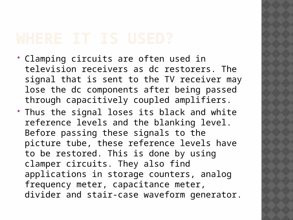
WHERE IT IS USED? Clamping circuits are often used in television
receivers as dc restorers. The signal that is sent to the TV receiver may lose the dc components after being passed through capacitively coupled amplifiers.
Thus the signal loses its black and white reference levels and the blanking level. Before passing these signals to the picture tube, these reference levels have to be restored. This is done by using clamper circuits. They also find applications in storage counters, analog frequency meter, capacitance meter, divider and stair-case waveform generator.

COMING TOWARDS OBJECTIVE NOW
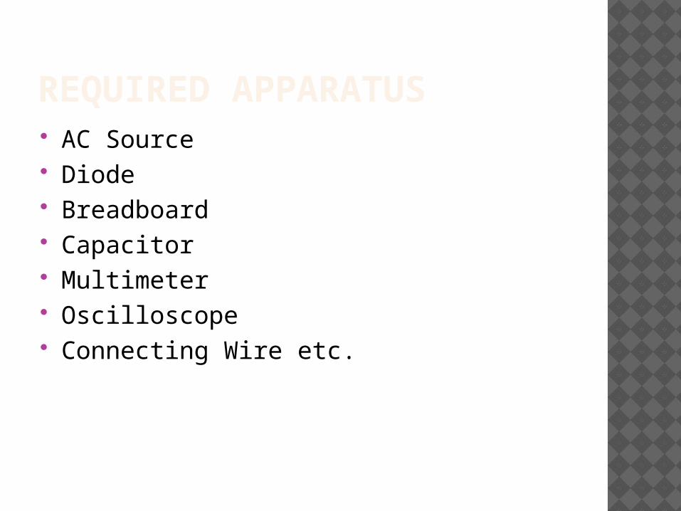
REQUIRED APPARATUS AC Source Diode Breadboard Capacitor Multimeter Oscilloscope Connecting Wire etc.
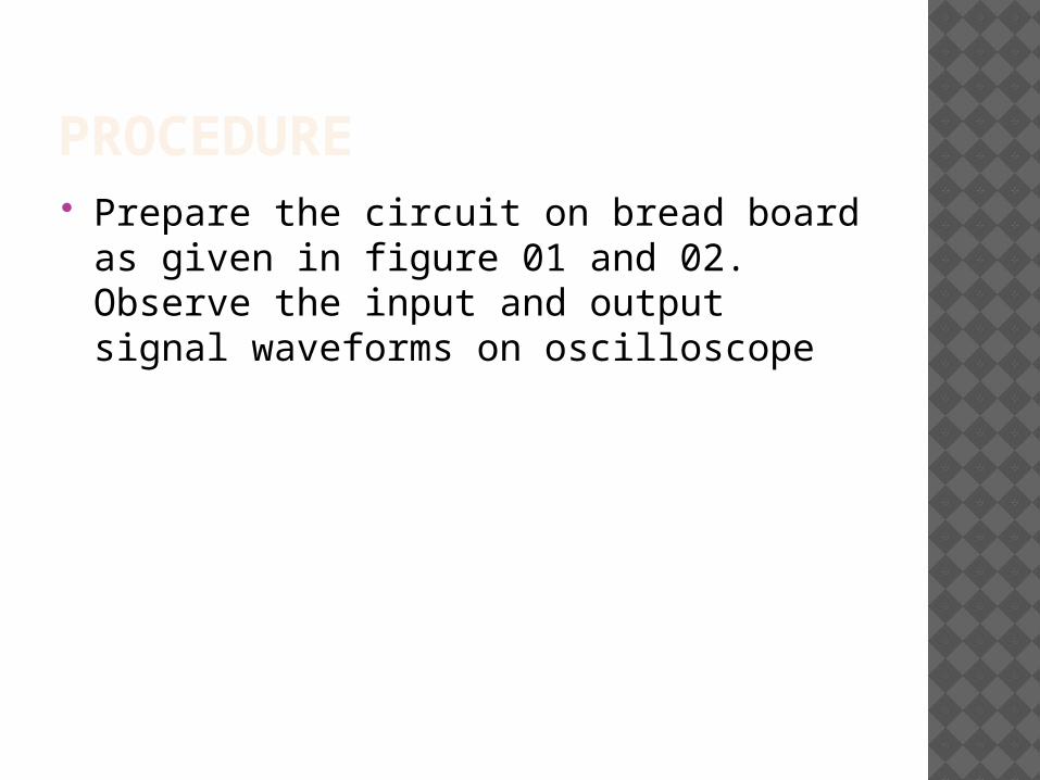
PROCEDURE Prepare the circuit on bread board as
given in figure 01 and 02. Observe the input and output signal waveforms on oscilloscope
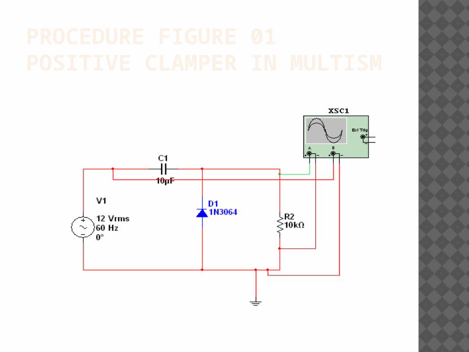
PROCEDURE FIGURE 01 POSITIVE CLAMPER IN MULTISM
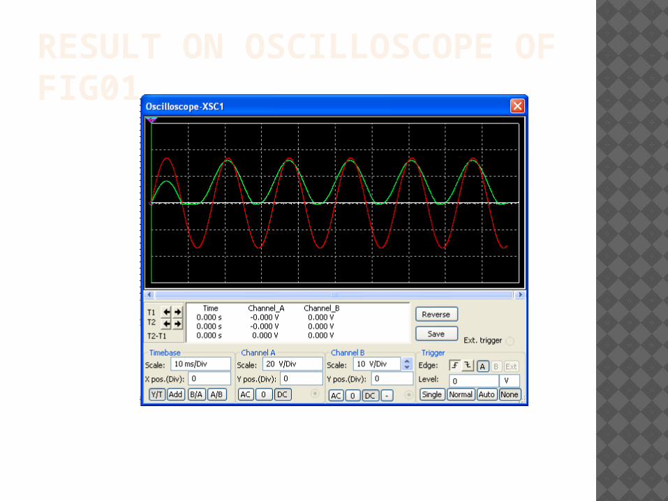
RESULT ON OSCILLOSCOPE OF FIG01
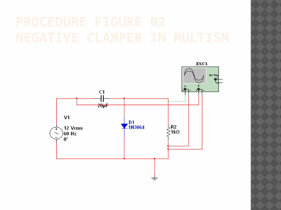
PROCEDURE FIGURE 02 NEGATIVE CLAMPER IN MULTISM
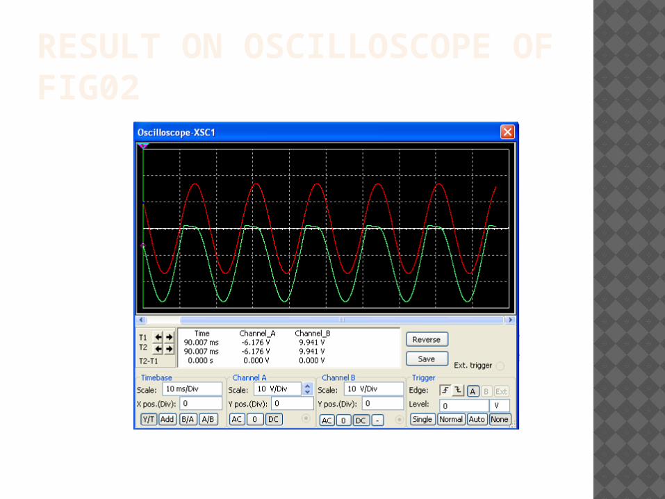
RESULT ON OSCILLOSCOPE OF FIG02
OBSERVATION Input and output signal waveforms
resemble with the waveforms as given in figure 01 and 02 for positive and negative diode clamper circuit respectively.

ANY QUERY ?