Embed Size (px)
Citation preview
01
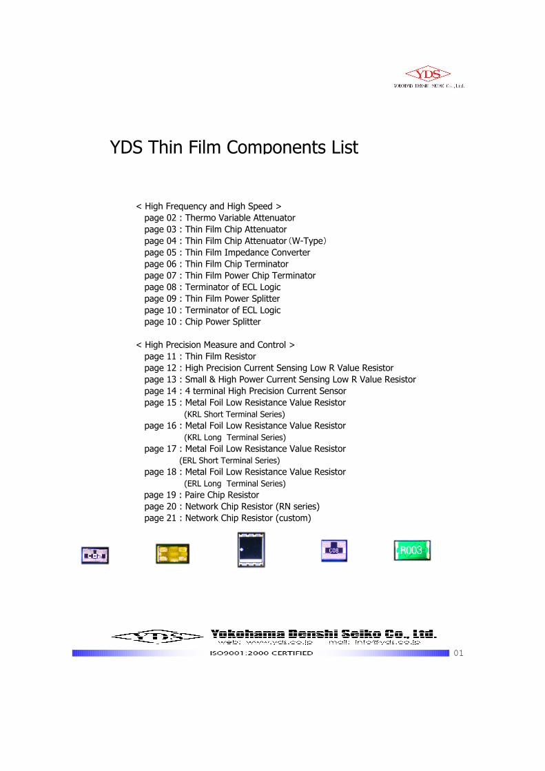
YDS Thin Film Components List
< High Frequency and High Speed >
page 02 : Thermo Variable Attenuator
page 03 : Thin Film Chip Attenuator
page 04 : Thin Film Chip Attenuator(W-Type)
page 05 : Thin Film Impedance Converter
page 06 : Thin Film Chip Terminator
page 07 : Thin Film Power Chip Terminator
page 08 : Terminator of ECL Logic
page 09 : Thin Film Power Splitter
page 10 : Terminator of ECL Logic
page 10 : Chip Power Splitter
< High Precision Measure and Control >
page 11 : Thin Film Resistor
page 12 : High Precision Current Sensing Low R Value Resistor
page 13 : Small & High Power Current Sensing Low R Value Resistor
page 14 : 4 terminal High Precision Current Sensor
page 15 : Metal Foil Low Resistance Value Resistor
(KRL Short Terminal Series)
page 16 : Metal Foil Low Resistance Value Resistor
(KRL Long Terminal Series)
page 17 : Metal Foil Low Resistance Value Resistor
(ERL Short Terminal Series)
page 18 : Metal Foil Low Resistance Value Resistor
(ERL Long Terminal Series)
page 19 : Paire Chip Resistor
page 20 : Network Chip Resistor (RN series)
page 21 : Network Chip Resistor (custom)
page 22 : Network Chip Resistor (RA series)
02
(mm)
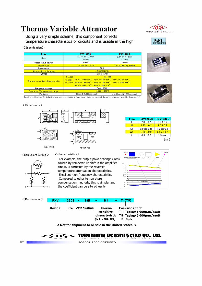
Thermo Variable Attenuator
High Freqency Circuit
temperature
+32
-2
-4
-6
+30
+26
+24
+28
gain
-20 0
+34
+36
Thermo Variable Attenuator
Input
(dB)
+75 C
Output
Amp. For example, the output power change (loss)
caused by temperature shift in the amplifier
circuit, is corrected by the reversed
temperature attenuation characteristics.
Excellent high frequency characteristics
Compared to other temperature
compensation methods, this is simpler and
the coefficient can be altered easily.
1
3
2
3
Using a very simple scheme, this component corrects
temperature characteristics of circuits and is usable in the high
frequency range.<Specification>
<Dimensions>
<Equivalent circuit> <Characteristics>
<Part number>
< Not for shipment to or sale in the United States. >
RoHScompliance
TypeTypeTypeType PBV1632SPBV1632SPBV1632SPBV1632S
3.2×1.6×1.5mm
(1206)
Rated input power 100mW
Attenuation 1~10(1dB step)・16dB
ImpedanceAttenuation tolerance
VSWRN1 to N8
1 to 3dB:
N1 to N9
Frequency rangeOperating Temperature range
Package min.20pcs/B 1,000pcs/reel
Detail specifications for individual part-number showing temperature characteristics of the attenuation are available. Contact us!
-40ºC~+100ºC
100pcs/B 1,000pcs/reel
Thermo sensitive characteristic
DC to 3GHz
ex.: 6dB
N1:0.0119dB/dB* N2:0.0088dB/dB* N3:0.0062dB/dB*
N4:0.0047dB/dB* N5:0.0041dB/dB* N6:0.0035dB/dB*
N7:0.0026dB/dB* N8:0.0019dB/dB*
PXV1220SPXV1220SPXV1220SPXV1220S
2.0×1.25×0.9mm
(0805)
63mW
Size
1~10dB(1dB step)
±0.5dB(@25)
<1.3(@25)
50Ω
PXVPXVPXVPXV 1220S1220S1220S1220S ---- 3dB3dB3dB3dB ---- N1N1N1N1 ---- T1(T5)T1(T5)T1(T5)T1(T5)
DeviceDeviceDeviceDevice SizeSizeSizeSize Packaging formPackaging formPackaging formPackaging formTTTT1111::::TapingTapingTapingTaping((((1111 ,,,,000000000000pcspcspcspcs////reelreelreelreel))))TTTT5555::::TapingTapingTapingTaping((((5555 ,,,,000000000000pcspcspcspcs////reelreelreelreel))))
((((NNNN1111~~~~NNNN8888・・・・NNNN9999)))) BBBB::::BulkBulkBulkBulk
AttenuationAttenuationAttenuationAttenuation ThermoThermoThermoThermosensitivesensitivesensitivesensitive
characteristiccharacteristiccharacteristiccharacteristic
TypeTypeTypeType PXV1220SPXV1220SPXV1220SPXV1220S PBV1632SPBV1632SPBV1632SPBV1632SL 2.0±0.2 3.2±0.2W 1.25±0.2 1.6±0.2
L1 0.65±0.35 1.0±0.25W1 0.35±0.2 0.55±0.2t 0.9±0.2 1.5max.
03
Thin Film Attenuator
W1
W WW
L1
t
PAT0510S
L1
W1
PAT0816PAT1220PAT1632
L
L
t
PAT3042S
W1
L1
L t
W2 W2
③
③
①
②
① ②
③③
②①
You can obtain excellent attenuation performance with one attenuator.
Very wide functional frequency range. Fit for circuit that handles different frequencies.
Compared to the attenuation circuit consisting of a combination of discrete resistors, with
this attenuator, the true designed value is attained due to much less parasitic
capacitance/inductance.
Due to its small size and equivalence to 3 discrete resistors, the space saving is significant
and the circuit reliability improves with fewer soldering joints.
We offer sizes from 1005(0402) to 3042(1612) with typical wrap around termination found in
common chip components, allowing easy mounting on boards and high reliability.
DC to 10GHz , 0402 (32mW) to 1612 (250mW) High Performance
<Specification>
<Dimensions>
3 3
1 2
<Equivalent circuit>
<Characteristics>
<Part number>
RoHScompliance
TypeTypeTypeType PAT0510SPAT0510SPAT0510SPAT0510S PAT0816PAT0816PAT0816PAT0816 PAT1220PAT1220PAT1220PAT1220 PAT1632PAT1632PAT1632PAT1632 PAT3042SPAT3042SPAT3042SPAT3042S
1.0×0.5×0.3mm 1.6 x 0.8 x 0.4mm 2.0×1.25×0.4mm 3.2×1.6×0.4mm 4.2×3.0×0.8mm
(0402) (0603) (0805) (1206) (1612)
Rated input power 32mW 64mW 100mW 125mW 250mW
Frequency range DC-10GHzDC-10GHzDC-10GHzDC-10GHz DC-10GHzDC-10GHzDC-10GHzDC-10GHz DC-10GHzDC-10GHzDC-10GHzDC-10GHz DC-3GHzDC-3GHzDC-3GHzDC-3GHz DC-3GHzDC-3GHzDC-3GHzDC-3GHz
0000~~~~10101010 0000~~~~10101010
16dB16dB16dB16dB 16161616・・・・20202020dBdBdBdB
Impedance 50Ω 50Ω 50Ω 50Ω 50Ω
VSWR1.3 (DC-6GHz)1.5 (6.1-10GHz)
1.3 (DC-6GHz)1.5 (6.1-10GHz)
1.3 (DC-6GHz)1.5 (6.1-10GHz)
1.5 (6-10GHz) 1.5 (6-10GHz) 1.5 (6-10GHz)
Operating Temperature range
±0.3dB (0-3dB)±0.5dB (4-7dB)
±1.0dB (8-10dB)±0.3dB
-55ºC~+125ºC
±0.3dB±0.5dB(16dB)
±0.3dB
1.3 1.2
If you require attenuation, frequency range, or tolerance out side of the product specifications, please contact us!
Size
Attenuation 0000~~~~10101010ddddBBBB 0000~~~~10101010ddddBBBB 0000~~~~10101010ddddBBBB
Attenuation tolerance
±0.3dB (0-3dB)±0.5dB (4-7dB)
±1.0dB (8-10dB)
PATPATPATPAT 1632163216321632 ---- CCCC ---- 3dB3dB3dB3dB ---- T1(T5)T1(T5)T1(T5)T1(T5)
DeviceDeviceDeviceDevice SizeSizeSizeSize ImpedanceImpedanceImpedanceImpedance AttenuationAttenuationAttenuationAttenuation Packaging formPackaging formPackaging formPackaging formTTTT1111::::TapingTapingTapingTaping((((1111 ,,,,000000000000pcspcspcspcs////reelreelreelreel))))TTTT5555::::TapingTapingTapingTaping((((5555 ,,,,000000000000pcspcspcspcs////reelreelreelreel))))
PAT0510S
(mm)
TypeTypeTypeType PAT0510SPAT0510SPAT0510SPAT0510S PAT0816PAT0816PAT0816PAT0816 PAT1220PAT1220PAT1220PAT1220 PAT1632PAT1632PAT1632PAT1632 PAT3042SPAT3042SPAT3042SPAT3042S
L 1.0±0.05 1.6±0.1 2.0±0.2 3.2±0.2 4.2±0.2
W 0.5±0.05 0.8±0.1 1.25±0.2 1.6±0.2 3.0±0.2
L1 0.29±0.05 0.5±0.15 0.6±0.2 1.0±0.2 0.5±0.2
W1 - 0.25±0.1 0.4±0.2 0.55±0.25 0.95±0.2
W2 - 0.15±0.1 0.4±0.2 0.4±0.25 0.95±0.2
W3 0.17±0.04 0.20±0.1 0.35±0.2 0.4±0.25 0.8±0.2
t 0.3±0.05 0.4±0.1 0.4±0.1 0.4±0.1 0.8±0.15
04
<W-Type>
Thin Film AttenuatorDC to 10GHz , High performance, high power application
<Specification>
<Dimensions>
<Equivalent circuit
<Part number>
<Characteristics>
tL
W W2
PAT3042
1
3
3
2
3
3
1
3
3
2
3
3
You can obtain highly accurate attenuation with
one attenuator.
Very wide functional frequency range. Fit for circuit
that handles different frequencies.
Compared to the attenuation circuit consisting of a
combination of discrete resistors, with this
attenuator, the true designed value is attained due
to much less parasitic capacitance/inductance.
One center signal terminal and two ground side
terminals offer easy integration within connectors
Rank DC~2GHz 2~5GHz 5~10GHz
0~10dB (A) ±0.1dB ±0.2dB ±0.4dB
(B) ±0.2dB ±0.3dB ±0.5dB
16, 20dB (B) ±0.2dB ±0.3dB ±0.5dB
Attenuation tolerance
RoHScompliance
L
W2
PAT4556
W
t
Type PAT3042 PAT4556
Attenuation(dB)
Rated input power 250mW 500mW
Impedance
Frequency range
OperatingTemperature range
Rated ambienttemperature
-55~+125
70
Packaging form1,000pcs/reel
50pcs/B
0~10, 16, 20
50Ω(C)
DC~10GHz
VSWR
<1.1(DC~2GHz)
<1.2(2~5GHz)
<1.3(5~10GHz)
PATPATPATPAT 3042304230423042 ---- CCCC ---- 3dB3dB3dB3dB ---- AAAA ---- T5T5T5T5
DeviceDeviceDeviceDevice SizeSizeSizeSize AttenuationAttenuationAttenuationAttenuation Packaging formPackaging formPackaging formPackaging formImpedanceImpedanceImpedanceImpedance TTTT1111::::TapingTapingTapingTaping((((1111 ,,,,000000000000pcspcspcspcs////reelreelreelreel))))
TTTT5555::::TapingTapingTapingTaping((((5555 ,,,,000000000000pcspcspcspcs////reelreelreelreel))))AttenuationAttenuationAttenuationAttenuationToleranceToleranceToleranceTolerance
PAT3042 PAT4556
L 4.2±0.2 5.6±0.2
W 3.0±0.2 4.5±0.2
W2 (0.9±0.1) (1.39±0.1)
t 0.8±0.15 0.8±0.15
SymbolSize(mm)
05
Thin Film Impedance Converter
High frequency, wide frequency range. Eliminates impedance
mismatching between circuits. Custom parts available.
<Specification>
<Dimensions>
<Equivalent circuit> <Characteristics>
<Part number>
t
W4
b
W1
W3
W
L
W2
a
50 - 75
3 3
1 2
This component matches impedance between circuits that differ
in their impedance allowing signals to transmit smoothly with
less reflection.
Thin film resistive elements and design for high frequency
provide a wide functional range from DC to high frequency.
Small size with typical wrap around termination found in
common chip components, allowing easy mounting and high
reliability
Non 50 ohm-75 ohm impedance matching components and
inter-circuit matching ATT possible.
RoHScompliance
PCHPCHPCHPCH 1632163216321632 ---- 50/7550/7550/7550/75 ---- T5T5T5T5
DeviceDeviceDeviceDevice SizeSizeSizeSize ImpedanceImpedanceImpedanceImpedance Packaging formPackaging formPackaging formPackaging formTTTT1111::::TapingTapingTapingTaping((((1111 ,,,,000000000000pcspcspcspcs////ree lree lree lree l))))TTTT5555::::TapingTapingTapingTaping((((5555 ,,,,000000000000pcspcspcspcs////ree lree lree lree l))))
Symbol Size
L 3.20±0.2
W 1.60±0.2
t 0.50±0.1
a 1.00±0.25
b 1.00±0.25
W1 0.60±0.25
W2 0.45±0.25
W3 0.40±0.25
W4 0.40±0.25(mm)
Type PCH1632
3.2×1.6×0.5mm
(1206)
Conversion impedance 50Ω/75Ω
Insertion loss 6±0.3dB
Rated power 125mW
Frequency range DC~1.5GHz
Rated ambient temperature 70°C
Operating temperature range -55~+125°C
Other impedance conversions and ATT for matching possible. Contact us!
Size
06
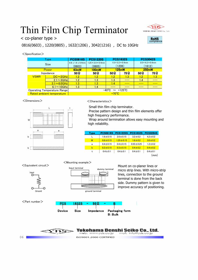
Thin Film Chip Terminator< co-planer type >
W
aa
b
b
L t
Input
Ground
信号ライン
グランド
ダミー
Small thin film chip terminator.
Precise pattern design and thin film elements offer
high frequency performance.
Wrap around termination allows easy mounting and
high reliability.
Mount on co-planer lines or
micro strip lines. With micro-strip
lines, connection to the ground
terminal is done from the back
side. Dummy pattern is given to
improve accuracy of positioning.
0816(0603) , 1220(0805) , 1632(1206) , 3042(1216) , DC to 10GHz
<Dimensions> <Characteristics>
<Equivalent circuit><Mounting example>
<Part number>
<Specification>
PCS0816SPCS0816SPCS0816SPCS0816S PCS1220SPCS1220SPCS1220SPCS1220S0.8 x 1.6 x 0.4mm 1.25×2.0×0.4mm
(0603) (0805)63mW63mW63mW63mW 100mW100mW100mW100mW50Ω50Ω50Ω50Ω 50Ω50Ω50Ω50Ω 50Ω50Ω50Ω50Ω 75Ω75Ω75Ω75Ω 50Ω50Ω50Ω50Ω 75Ω75Ω75Ω75Ω
VSWR DC~2GHz 1.2 1.2 1.2 1.3 1.2 1.32.1~3GHz 1.2 1.3 1.3 --- 1.4 ---
3.1~6.0GHz 1.3 1.3 1.4 --- --- ---6.1~10GHz 1.3 1.4 --- --- --- ---
Operating Temperature Range -40 ~ +125Rated ambient temperature +70
Power 125mW125mW125mW125mW 250mW250mW250mW250mWInpedance
Size1.6×3.2×0.4mm 3.0×4.2×0.4mm
(1206) (1612)
Type PCS1632SPCS1632SPCS1632SPCS1632S PCS3042SPCS3042SPCS3042SPCS3042S
RoHScompliance
PCSPCSPCSPCS 1632S1632S1632S1632S ---- 50Ω50Ω50Ω50Ω ---- BBBB
DeviceDeviceDeviceDevice SizeSizeSizeSize ImpedanceImpedanceImpedanceImpedance Packaging formPackaging formPackaging formPackaging formBBBB::::BulkBulkBulkBulk
Input terminal dummy terminal
ground terminal
TypeTypeTypeType PCS0816SPCS0816SPCS0816SPCS0816S PCS1220SPCS1220SPCS1220SPCS1220S PCS1632SPCS1632SPCS1632SPCS1632S PCS3264SPCS3264SPCS3264SPCS3264S
L 1.6±0.15 2.0±0.15 3.2±0.2 4.2±0.2
W 0.8±0.15 1.25±0.15 1.6±0.2 3.0±0.2
a 0.4±0.15 0.4±0.15 0.55±0.25 1.2±0.2
b 0.2±0.15 0.3±0.15 0.4±0.2 0.4±0.2
t 0.4±0.1 0.4±0.1 0.4±0.1 0.4±0.1
(mm)
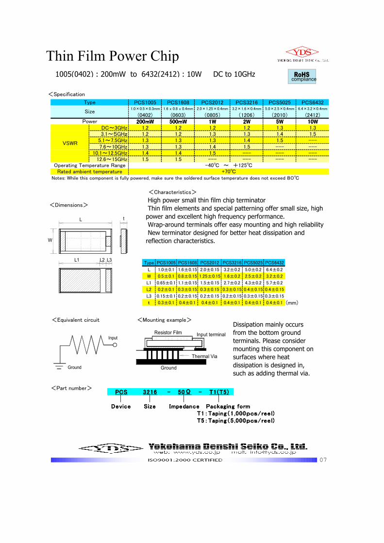
07
Thin Film Power Chip1005(0402) : 200mW to 6432(2412) : 10W DC to 10GHz
<Specification>
<Dimensions>
<Equivalent circuit>
<Mounting example>
<Part number>
<Characteristics>
W
L1 L2 L3
L t
High power small thin film chip terminator
Thin film elements and special patterning offer small size, high
power and excellent high frequency performance.
Wrap-around terminals offer easy mounting and high reliability
New terminator designed for better heat dissipation and
reflection characteristics.
Input
Ground
Input terminalResistor Film
Thermal Via
Ground
Dissipation mainly occurs
from the bottom ground
terminals. Please consider
mounting this component on
surfaces where heat
dissipation is designed in,
such as adding thermal via.
PCS1005 PCS1608 PCS2012 PCS3216 PCS5025 PCS64321.0×0.5×0.3mm 1.6 x 0.8 x 0.4mm 2.0×1.25×0.4mm 3.2×1.6×0.4mm 5.0×2.5×0.4mm 6.4×3.2×0.4mm
(0402) (0603) (0805) (1206) (2010) (2412)200mW200mW200mW200mW 500mW500mW500mW500mW 1W1W1W1W 2W2W2W2W 5W5W5W5W 10W10W10W10W
DC~3GHz 1.2 1.2 1.2 1.2 1.3 1.33.1~5GHz 1.2 1.2 1.3 1.3 1.4 1.5
5.1~7.5GHz 1.3 1.3 1.3 1.4 1.5 ---7.6~10GHz 1.3 1.3 1.4 1.5 --- ---
10.1~12.5GHz 1.4 1.4 1.5 --- --- ---12.6~15GHz 1.5 1.5 --- --- --- ---
Notes: While this component is fully powered, make sure the soldered surface temperature does not exceed 80
Operating Temperature Range -40 ~ +125Rated ambient temperature +70
Type
Size
Power
VSWR
Type PCS1005 PCS1608 PCS2012 PCS3216 PCS5025 PCS6432
L 1.0±0.1 1.6±0.15 2.0±0.15 3.2±0.2 5.0±0.2 6.4±0.2
W 0.5±0.1 0.8±0.15 1.25±0.15 1.6±0.2 2.5±0.2 3.2±0.2
L1 0.65±0.1 1.1±0.15 1.5±0.15 2.7±0.2 4.3±0.2 5.7±0.2
L2 0.2±0.1 0.3±0.15 0.3±0.15 0.3±0.15 0.4±0.15 0.4±0.15
L3 0.15±0.1 0.2±0.15 0.2±0.15 0.2±0.15 0.3±0.15 0.3±0.15
t 0.3±0.1 0.4±0.1 0.4±0.1 0.4±0.1 0.4±0.1 0.4±0.1 (mm)
RoHScompliance
PCSPCSPCSPCS 3216321632163216 ---- 50Ω50Ω50Ω50Ω ---- T1(T5)T1(T5)T1(T5)T1(T5)
DeviceDeviceDeviceDevice SizeSizeSizeSize ImpedanceImpedanceImpedanceImpedance Packaging formPackaging formPackaging formPackaging formTTTT1111::::TapingTapingTapingTaping((((1111 ,,,,000000000000pcspcspcspcs////ree lree lree lree l))))TTTT5555::::TapingTapingTapingTaping((((5555 ,,,,000000000000pcspcspcspcs////ree lree lree lree l))))
08
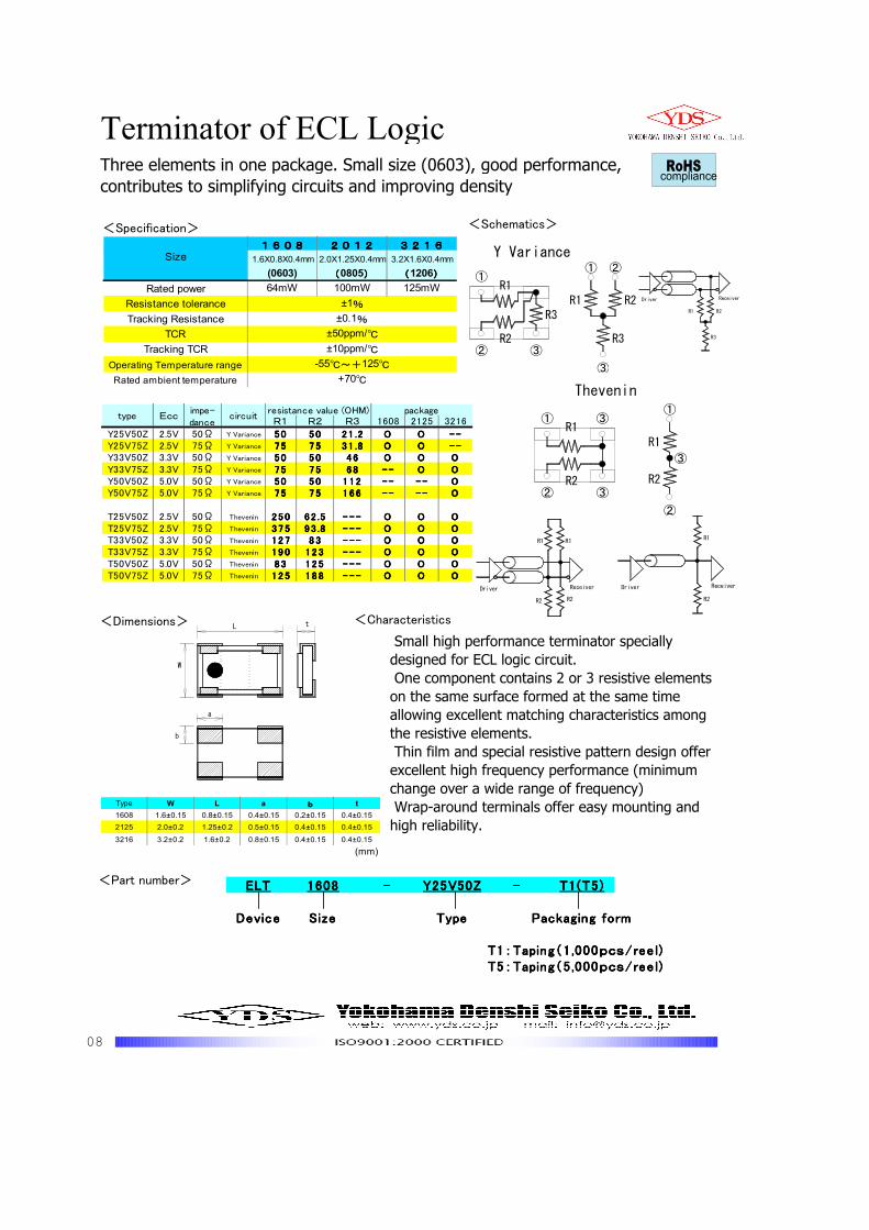
Terminator of ECL LogicThree elements in one package. Small size (0603), good performance,
contributes to simplifying circuits and improving density
<Specification> <Schematics>
Y Variance
② ③
R3
R2
①R1
R1 R2
③
R3
① ②
ReceiverDriver
R3
R1 R2
Thevenin
R2③②
③①R1
R1
R2
②
③
①
R2
R1
Driver
R2
R1
DriverReceiver
R2
Receiver
R1
<Dimensions> <Characteristics>
<Part number>
L
a
b
W
t
Small high performance terminator specially
designed for ECL logic circuit.
One component contains 2 or 3 resistive elements
on the same surface formed at the same time
allowing excellent matching characteristics among
the resistive elements.
Thin film and special resistive pattern design offer
excellent high frequency performance (minimum
change over a wide range of frequency)
Wrap-around terminals offer easy mounting and
high reliability.
RoHScompliance
R1 R2 R3 1608 2125 3216
Y25V50Z 2.5V 50Ω Y Variance 50505050 50505050 21 .221 .221 .221 .2 OOOO OOOO --------Y25V75Z 2.5V 75Ω Y Variance 75757575 75757575 31 .831 .831 .831 .8 OOOO OOOO --------Y33V50Z 3.3V 50Ω Y Variance 50505050 50505050 46464646 OOOO OOOO OOOOY33V75Z 3.3V 75Ω Y Variance 75757575 75757575 68686868 -------- OOOO OOOOY50V50Z 5.0V 50Ω Y Variance 50505050 50505050 112112112112 -------- -------- OOOOY50V75Z 5.0V 75Ω Y Variance 75757575 75757575 166166166166 -------- -------- OOOO
T25V50Z 2.5V 50Ω Thevenin 250250250250 62 .562 .562 .562 .5 - ----------- OOOO OOOO OOOOT25V75Z 2.5V 75Ω Thevenin 375375375375 93 .893 .893 .893 .8 - ----------- OOOO OOOO OOOOT33V50Z 3.3V 50Ω Thevenin 127127127127 83838383 ------------ OOOO OOOO OOOOT33V75Z 3.3V 75Ω Thevenin 190190190190 123123123123 ------------ OOOO OOOO OOOOT50V50Z 5.0V 50Ω Thevenin 83838383 125125125125 ------------ OOOO OOOO OOOOT50V75Z 5.0V 75Ω Thevenin 125125125125 188188188188 ------------ OOOO OOOO OOOO
impe-dance
circuitresistance value (OHM) package
type Ecc
ELTELTELTELT 1608160816081608 ---- Y25V50ZY25V50ZY25V50ZY25V50Z ---- T1(T5)T1(T5)T1(T5)T1(T5)
DeviceDeviceDeviceDevice SizeSizeSizeSize TypeTypeTypeType Packaging formPackaging formPackaging formPackaging form
TTTT1111::::TapingTapingTapingTaping((((1111 ,,,,000000000000pcspcspcspcs//// ree lree lree lree l))))TTTT5555::::TapingTapingTapingTaping((((5555 ,,,,000000000000pcspcspcspcs//// ree lree lree lree l))))
1608160816081608 2012201220122012 3216321632163216
1.6X0.8X0.4mm 2.0X1.25X0.4mm 3.2X1.6X0.4mm
(0603) ((((0805)))) ((((1206))))
Rated power 64mW 100mW 125mW
Resistance tolerance
Tracking Resistance
TCR
Tracking TCR
Operating Temperature range
Rated ambient temperature
±10ppm/
-55~+125
+70
Size
±1%
±0.1%
±50ppm/
Type W L a bbbb t
1608 1.6±0.15 0.8±0.15 0.4±0.15 0.2±0.15 0.4±0.15
2125 2.0±0.2 1.25±0.2 0.5±0.15 0.4±0.15 0.4±0.15
3216 3.2±0.2 1.6±0.2 0.8±0.15 0.4±0.15 0.4±0.15
(mm)
09
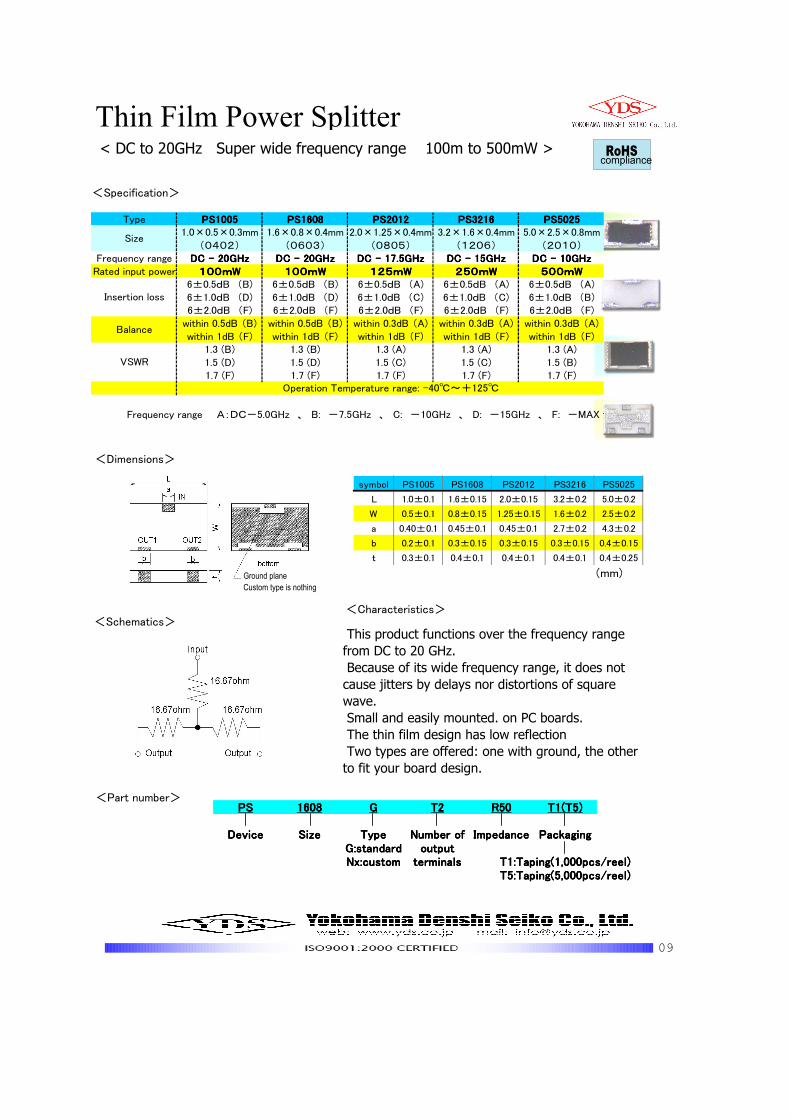
Thin Film Power Splitter< DC to 20GHz Super wide frequency range 100m to 500mW >
<Specification>
<Dimensions>
<Schematics>
<Part number>
<Characteristics>
This product functions over the frequency range
from DC to 20 GHz.
Because of its wide frequency range, it does not
cause jitters by delays nor distortions of square
wave.
Small and easily mounted. on PC boards.
The thin film design has low reflection
Two types are offered: one with ground, the other
to fit your board design.
RoHScompliance
Ground plane
Custom type is nothing
Type PS1005PS1005PS1005PS1005 PS1608PS1608PS1608PS1608 PS2012PS2012PS2012PS2012 PS3216PS3216PS3216PS3216 PS5025PS5025PS5025PS50251.0×0.5×0.3mm 1.6×0.8×0.4mm 2.0×1.25×0.4mm 3.2×1.6×0.4mm 5.0×2.5×0.8mm
(0402) (0603) (0805) (1206) (2010)Frequency range DC - 20GHzDC - 20GHzDC - 20GHzDC - 20GHz DC - 20GHzDC - 20GHzDC - 20GHzDC - 20GHz DC - 17.5GHzDC - 17.5GHzDC - 17.5GHzDC - 17.5GHz DC - 15GHzDC - 15GHzDC - 15GHzDC - 15GHz DC - 10GHzDC - 10GHzDC - 10GHzDC - 10GHz
Rated input power 100100100100mmmmWWWW 100100100100mmmmWWWW 125125125125mmmmWWWW 250250250250mmmmWWWW 500500500500mmmmWWWW6±0.5dB (B) 6±0.5dB (B) 6±0.5dB (A) 6±0.5dB (A) 6±0.5dB (A)
6±1.0dB (D) 6±1.0dB (D) 6±1.0dB (C) 6±1.0dB (C) 6±1.0dB (B)6±2.0dB (F) 6±2.0dB (F) 6±2.0dB (F) 6±2.0dB (F) 6±2.0dB (F)
within 0.5dB (B) within 0.5dB (B) within 0.3dB (A) within 0.3dB (A) within 0.3dB (A)
within 1dB (F) within 1dB (F) within 1dB (F) within 1dB (F) within 1dB (F)1.3 (B) 1.3 (B) 1.3 (A) 1.3 (A) 1.3 (A)
1.5 (D) 1.5 (D) 1.5 (C) 1.5 (C) 1.5 (B)1.7 (F) 1.7 (F) 1.7 (F) 1.7 (F) 1.7 (F)
Frequency range A:DC-5.0GHz 、 B: -7.5GHz 、 C: -10GHz 、 D: -15GHz 、 F: -MAX frequency
Operation Temperature range: -40~+125
Size
Insertion loss
Balance
VSWR
PSPSPSPS 1608160816081608 GGGG T2T2T2T2 R50R50R50R50 T1(T5)T1(T5)T1(T5)T1(T5)
DeviceDeviceDeviceDevice SizeSizeSizeSize TypeTypeTypeType Number ofNumber ofNumber ofNumber of ImpedanceImpedanceImpedanceImpedance PackagingPackagingPackagingPackagingG:standardG:standardG:standardG:standard outputoutputoutputoutputNx:customNx:customNx:customNx:custom terminalsterminalsterminalsterminals T1:Taping(1,000pcs/reel)T1:Taping(1,000pcs/reel)T1:Taping(1,000pcs/reel)T1:Taping(1,000pcs/reel)
T5:Taping(5,000pcs/reel)T5:Taping(5,000pcs/reel)T5:Taping(5,000pcs/reel)T5:Taping(5,000pcs/reel)
symbol PS1005 PS1608 PS2012 PS3216 PS5025
L 1.0±0.1 1.6±0.15 2.0±0.15 3.2±0.2 5.0±0.2
W 0.5±0.1 0.8±0.15 1.25±0.15 1.6±0.2 2.5±0.2
a 0.40±0.1 0.45±0.1 0.45±0.1 2.7±0.2 4.3±0.2
b 0.2±0.1 0.3±0.15 0.3±0.15 0.3±0.15 0.4±0.15
t 0.3±0.1 0.4±0.1 0.4±0.1 0.4±0.1 0.4±0.25
(mm)
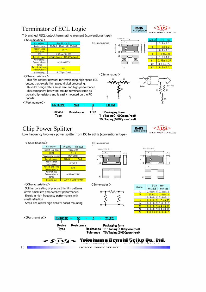
10
Y branched PECL output terminating element (conventional type)
Terminator of ECL Logic
<Specification><Dimensions>
W
W1
b
W3
W2
aL
RN1632F-N23-F-C
t
<Characteristics> Thin film resistor network for terminating high speed ECL
output that excels high speed digital processing.
This film design offers small size and high performance.
This component has wrap-around terminals same as
typical chip resistors and is easily mounted on the PC
boards.
<Schematics>
31 2
R2
R3R1
ReceiverDriver
R3
R1 R2
<Part number>
Chip Power SplitterLow frequency two-way power splitter from DC to 2GHz (conventional type)
<Specification> <Dimensions>
W3
a
W2
W
W1
RN1220E-50-F
tL
b
W3
RN1632E-50-F
a
W2
W
W1
t
L
Splitter consisting of precise thin film patterns
offers small size and excellent performance.
Excels in high frequency performance with
small reflection
Small size allows high density board mounting.
<Schematics><Characteristics>
<Part number>
Parameter Specification
Resistance R1=50Ω、R2=46.4Ω、R3=50ΩResistancetolerance ±1%(F)
TCR ±50ppm/(C)
Rated power 42mW/element、125mW/networkOperating
TemperatureRange
-55~+125
Rated ambienttemperature 70
Packaging 5,000pcs/reel
RN1632ERN1632ERN1632ERN1632E ---- 50505050 ---- FFFF ---- T1(T5)T1(T5)T1(T5)T1(T5)
Packaging formPackaging formPackaging formPackaging formTTTT1111::::TapingTapingTapingTaping((((1111,,,,000000000000pcspcspcspcs////reelreelreelreel))))TTTT5555::::TapingTapingTapingTaping((((5555,,,,000000000000pcspcspcspcs////reelreelreelreel))))
ResistanceResistanceResistanceResistanceResistanceResistanceResistanceResistanceToleranceToleranceToleranceTolerance
DeviceDeviceDeviceDeviceTypeTypeTypeType
RN1632FRN1632FRN1632FRN1632F ---- N23N23N23N23 ---- BBBB ---- T1(T5)T1(T5)T1(T5)T1(T5)
ResistanceResistanceResistanceResistance TCRTCRTCRTCR Packaging formPackaging formPackaging formPackaging formTTTT1111::::TapingTapingTapingTaping((((1111,,,,000000000000pcspcspcspcs////reelreelreelreel))))TTTT5555::::TapingTapingTapingTaping((((5555,,,,000000000000pcspcspcspcs////reelreelreelreel))))
DeviceDeviceDeviceDeviceTypeTypeTypeType
Symbol Size (mm)
L 3.2±0.2
W 1.6±0.2
t 0.4±0.1
a 1.0±0.25
b 1.0±0.2
W1 0.55±0.25
W2 0.4±0.25
W3 0.4±0.2
RN1220E RN1632EL 2.0±0.1 3.2±0.2W 1.25±0.1 1.6±0.2t 0.4±0.1 0.4±0.1a 0.5±0.2 1.0±0.25b 0.6±0.2 1.0±0.2W1 0.3±0.2 0.4±0.25W2 0.3±0.2 0.4±0.25W3 0.35±0.2 0.4±0.2
Size (mm)Symbol
Parameter RN1220E RN1632E
Insertion loss
VSWR
Frequency renge
Rated power 100mW 125mWResistancetolerance
Rated ambienttemperatureOperatingTemperature
Range
Packaging
70
-55~+125
1,000・5,000pcs/reel
6±0.3dB
<1.3
DC~2GHz
±1%(F)
RoHScompliance
RoHScompliance
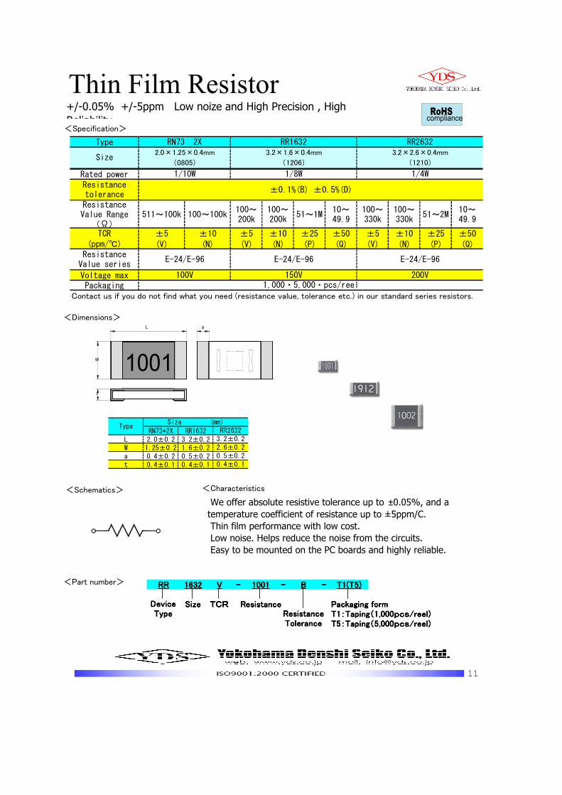
11
Thin Film Resistor+/-0.05% +/-5ppm Low noize and High Precision , High
Reliability<Specification>
<Dimensions>
L a
W 1001t
<Characteristics> We offer absolute resistive tolerance up to ±0.05%, and a
temperature coefficient of resistance up to ±5ppm/C.
Thin film performance with low cost.
Low noise. Helps reduce the noise from the circuits.
Easy to be mounted on the PC boards and highly reliable.
<Schematics>
<Part number> RRRRRRRR 1632163216321632 VVVV ---- 1001100110011001 ---- BBBB ---- T1(T5)T1(T5)T1(T5)T1(T5)
SizeSizeSizeSize TCRTCRTCRTCR ResistanceResistanceResistanceResistance Packaging formPackaging formPackaging formPackaging formTTTT1111::::TapingTapingTapingTaping((((1111,,,,000000000000pcspcspcspcs////reelreelreelreel))))TTTT5555::::TapingTapingTapingTaping((((5555,,,,000000000000pcspcspcspcs////reelreelreelreel))))
DeviceDeviceDeviceDeviceTypeTypeTypeType ResistanceResistanceResistanceResistance
ToleranceToleranceToleranceTolerance
RN73*2X RR1632 RR2632
L 2.0±0.2 3.2±0.2 3.2±0.2
W 1.25±0.2 1.6±0.2 2.6±0.2
a 0.4±0.2 0.5±0.2 0.5±0.2
t 0.4±0.1 0.4±0.1 0.4±0.1
TypeSize (mm)
Type
Rated power
ResistanceValue Range
(Ω)511~100k 100~100k
100~200k
100~200k
51~1M10~49.9
100~330k
100~330k
51~2M10~49.9
TCR ±5 ±10 ±5 ±10 ±25 ±50 ±5 ±10 ±25 ±50(ppm/) (V) (N) (V) (N) (P) (Q) (V) (N) (P) (Q)
Voltage maxPackaging
Contact us if you do not find what you need (resistance value, tolerance etc.) in our standard series resistors.
1,000・5,000・pcs/reel
E-24/E-96
100V 150V 200V
1/4W
Resistancetolerance
±0.1%(B) ±0.5%(D)
E-24/E-96
RR2632
Size3.2×1.6×0.4mm 3.2×2.6×0.4mm
(1206) (1210)
ResistanceValue series
E-24/E-96
RN73 2X2.0×1.25×0.4mm
(0805)
1/10W
RR1632
1/8W
RoHScompliance
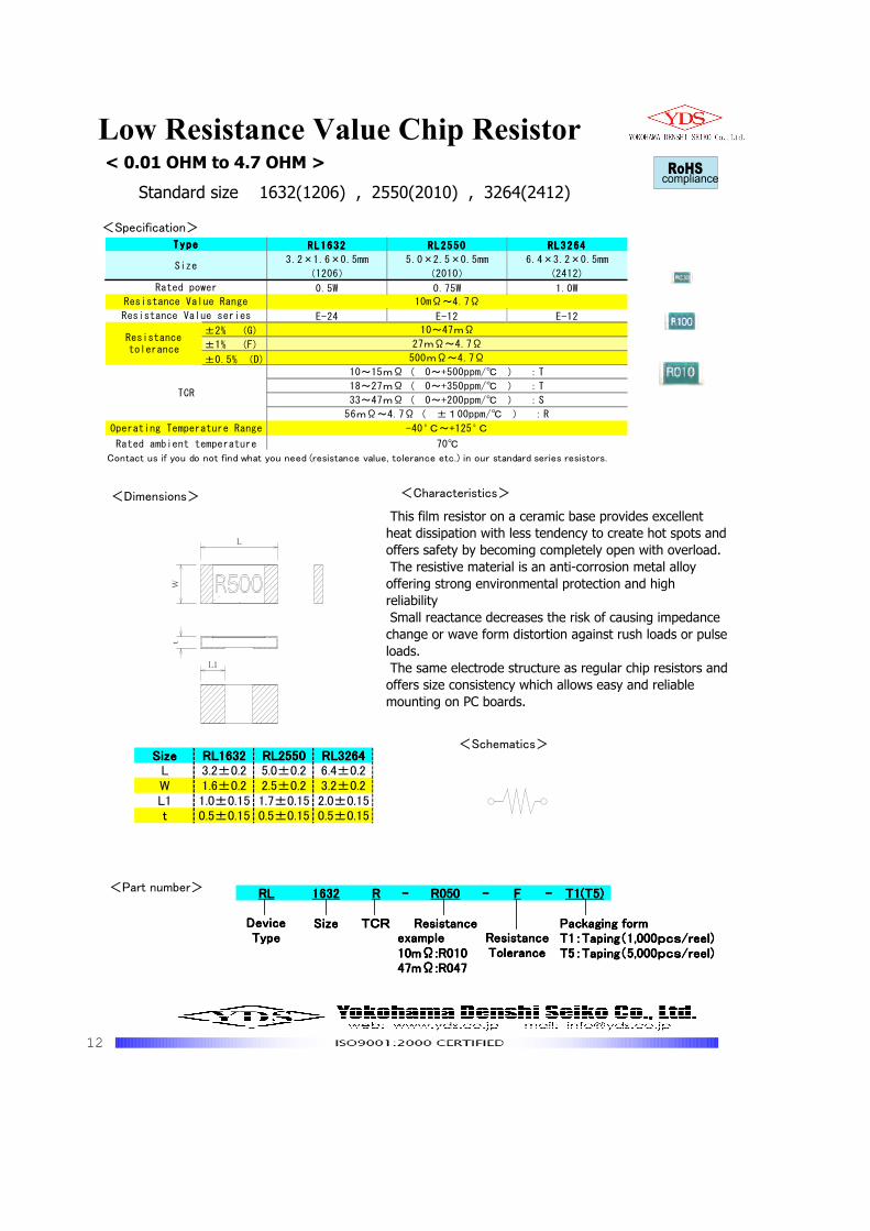
12
Low Resistance Value Chip Resistor
Standard size 1632(1206) , 2550(2010) , 3264(2412)
<Specification>
<Dimensions>
<Part number>
<Characteristics>
This film resistor on a ceramic base provides excellent
heat dissipation with less tendency to create hot spots and
offers safety by becoming completely open with overload.
The resistive material is an anti-corrosion metal alloy
offering strong environmental protection and high
reliability
Small reactance decreases the risk of causing impedance
change or wave form distortion against rush loads or pulse
loads.
The same electrode structure as regular chip resistors and
offers size consistency which allows easy and reliable
mounting on PC boards.
<Schematics>
L
W
L1
t
RLRLRLRL 1632163216321632 RRRR ---- R050R050R050R050 ---- FFFF ---- T1(T5)T1(T5)T1(T5)T1(T5)
SizeSizeSizeSize TCRTCRTCRTCR ResistanceResistanceResistanceResistance Packaging formPackaging formPackaging formPackaging formTTTT1111::::TapingTapingTapingTaping((((1111,,,,000000000000pcspcspcspcs////reelreelreelreel))))
10mΩ:R01010mΩ:R01010mΩ:R01010mΩ:R010 TTTT5555::::TapingTapingTapingTaping((((5555,,,,000000000000pcspcspcspcs////reelreelreelreel))))47mΩ:R04747mΩ:R04747mΩ:R04747mΩ:R047
DeviceDeviceDeviceDeviceTypeTypeTypeType ResistanceResistanceResistanceResistance
ToleranceToleranceToleranceToleranceexampleexampleexampleexample
SizeSizeSizeSize RL1632RL1632RL1632RL1632 RL2550RL2550RL2550RL2550 RL3264RL3264RL3264RL3264L 3.2±0.2 5.0±0.2 6.4±0.2W 1.6±0.2 2.5±0.2 3.2±0.2L1 1.0±0.15 1.7±0.15 2.0±0.15t 0.5±0.15 0.5±0.15 0.5±0.15
RoHScompliance
< 0.01 OHM to 4.7 OHM >
RL1632RL1632RL1632RL1632 RL2550RL2550RL2550RL2550 RL3264RL3264RL3264RL3264
3.2×1.6×0.5mm 5.0×2.5×0.5mm 6.4×3.2×0.5mm
(1206) (2010) (2412)
0.5W 0.75W 1.0W
E-24 E-12 E-12
±2% (G)
±1% (F)
±0.5% (D)
Contact us if you do not find what you need (resistance value, tolerance etc.) in our standard series resistors.
TypeTypeTypeType
Size
Rated power
Resistance Value Range 10mΩ~4.7Ω
Resistance Value series
Resistancetolerance
10~47mΩ
27mΩ~4.7Ω
500mΩ~4.7Ω
TCR
10~15mΩ ( 0~+500ppm/ ) :T
18~27mΩ ( 0~+350ppm/ ) :T
33~47mΩ ( 0~+200ppm/ ) :S
56mΩ~4.7Ω ( ±100ppm/ ) :R
Operating Temperature Range -40ºC~+125ºC
Rated ambient temperature 70
13
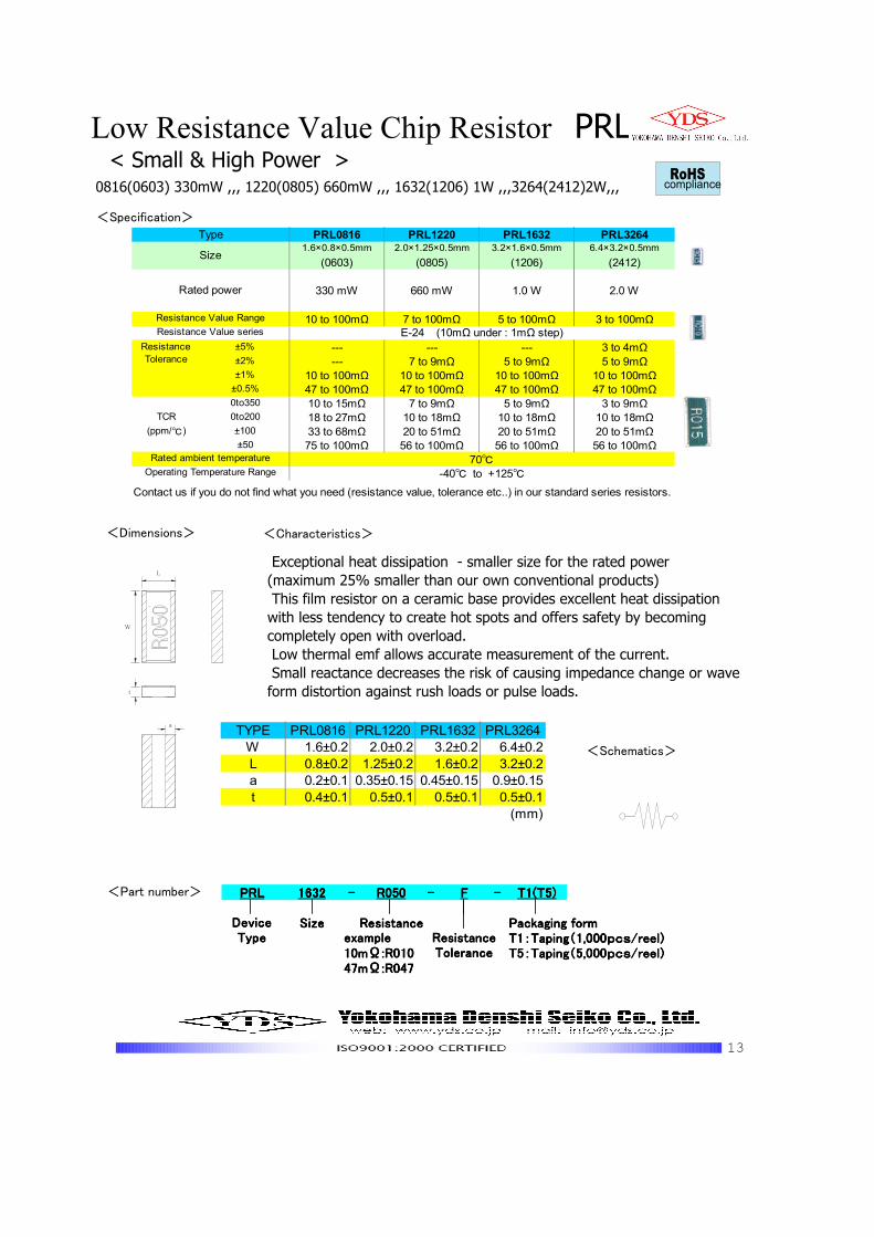
Low Resistance Value Chip Resistor PRL
< Small & High Power >0816(0603) 330mW ,,, 1220(0805) 660mW ,,, 1632(1206) 1W ,,,3264(2412)2W,,,
<Specification>
<Dimensions> <Characteristics>
<Schematics>
<Part number>
Exceptional heat dissipation - smaller size for the rated power
(maximum 25% smaller than our own conventional products)
This film resistor on a ceramic base provides excellent heat dissipation
with less tendency to create hot spots and offers safety by becoming
completely open with overload.
Low thermal emf allows accurate measurement of the current.
Small reactance decreases the risk of causing impedance change or wave
form distortion against rush loads or pulse loads.
W
t
a
L
PRLPRLPRLPRL 1632163216321632 ---- R050R050R050R050 ---- FFFF ---- T1(T5)T1(T5)T1(T5)T1(T5)
SizeSizeSizeSize ResistanceResistanceResistanceResistance Packaging formPackaging formPackaging formPackaging formTTTT1111::::TapingTapingTapingTaping((((1111,,,,000000000000pcspcspcspcs////reelreelreelreel))))
10mΩ:R01010mΩ:R01010mΩ:R01010mΩ:R010 TTTT5555::::TapingTapingTapingTaping((((5555,,,,000000000000pcspcspcspcs////reelreelreelreel))))47mΩ:R04747mΩ:R04747mΩ:R04747mΩ:R047
DeviceDeviceDeviceDeviceTypeTypeTypeType ResistanceResistanceResistanceResistance
ToleranceToleranceToleranceToleranceexampleexampleexampleexample
RoHScompliance
PRL0816 PRL1220 PRL1632 PRL32641.6×0.8×0.5mm 2.0×1.25×0.5mm 3.2×1.6×0.5mm 6.4×3.2×0.5mm
(0603) (0805) (1206) (2412)
330 mW 660 mW 1.0 W 2.0 W
10 to 100mΩ 7 to 100mΩ 5 to 100mΩ 3 to 100mΩ
±5% --- --- --- 3 to 4mΩ±2% --- 7 to 9mΩ 5 to 9mΩ 5 to 9mΩ±1% 10 to 100mΩ 10 to 100mΩ 10 to 100mΩ 10 to 100mΩ
±0.5% 47 to 100mΩ 47 to 100mΩ 47 to 100mΩ 47 to 100mΩ0to350 10 to 15mΩ 7 to 9mΩ 5 to 9mΩ 3 to 9mΩ
TCR 0to200 18 to 27mΩ 10 to 18mΩ 10 to 18mΩ 10 to 18mΩ(ppm/) ±100 33 to 68mΩ 20 to 51mΩ 20 to 51mΩ 20 to 51mΩ
±50 75 to 100mΩ 56 to 100mΩ 56 to 100mΩ 56 to 100mΩ
Contact us if you do not find what you need (resistance value, tolerance etc..) in our standard series resistors.
Operating Temperature Range -40 to +125
Resistance
Tolerance
Resistance Value series E-24 (10mΩ under : 1mΩ step)
Rated ambient temperature 70
Type
Size
Rated power
Resistance Value Range
TYPE PRL0816 PRL1220 PRL1632 PRL3264
W 1.6±0.2 2.0±0.2 3.2±0.2 6.4±0.2
L 0.8±0.2 1.25±0.2 1.6±0.2 3.2±0.2
a 0.2±0.1 0.35±0.15 0.45±0.15 0.9±0.15
t 0.4±0.1 0.5±0.1 0.5±0.1 0.5±0.1
(mm)
14
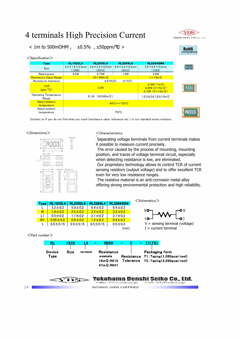
4 terminals High Precision Current
< 1m to 500mOHM , ±0.5% , ±50ppm/ >
<Specification>
<Dimensions> <Characteristics> Separating voltage terminals from current terminals makes
it possible to measure current precisely.
The error caused by the process of mounting, mounting
position, and traces of voltage terminal circuit, especially
when detecting resistance is low, are eliminated.
Our proprietary technology allows to control TCR of current
sensing resistors (output voltage) and to offer excellent TCR
even for very low resistance ranges.
The resistive material is an anti-corrosion metal alloy
offering strong environmental protection and high reliability.
<Schematics>
<Part number>
I
VI
= 電圧端子
= 電流端子
V
I
V
TypeTypeTypeType RL1632L4RL1632L4RL1632L4RL1632L4 RL2550L4RL2550L4RL2550L4RL2550L4 RL3264L4RL3264L4RL3264L4RL3264L4 RL3264SW4RL3264SW4RL3264SW4RL3264SW4L 3.2±0.2 5.0±0.2 6.4±0.2 6.4±0.2W 1.6±0.2 2.5±0.2 3.2±0.2 3.2±0.2L1 0.5±0.2 1.7±0.2 2.1±0.2 2.7±0.2W1 0.55±0.2 0.9±0.2 1.2±0.2 0.4±0.2t 0.5±0.15 0.5±0.15 0.5±0.15 0.5±0.2
(mm)
RoHScompliance
RLRLRLRL 1632163216321632 L4L4L4L4 ---- R050R050R050R050 ---- FFFF ---- T1(T5)T1(T5)T1(T5)T1(T5)
SizeSizeSizeSize te rmin alte rmin alte rmin alte rmin al ResistanceResistanceResistanceResistance Packaging formPackaging formPackaging formPackaging formTTTT1111::::TapingTapingTapingTaping((((1111 ,,,, 000000000000pcspcspcspcs//// ree lree lree lree l ))))
10mΩ:R01010mΩ:R01010mΩ:R01010mΩ:R010 TTTT5555::::TapingTapingTapingTaping((((5555 ,,,, 000000000000pcspcspcspcs//// ree lree lree lree l ))))
47mΩ:R04747mΩ:R04747mΩ:R04747mΩ:R047
DeviceDeviceDeviceDeviceTypeTypeTypeType exampleexampleexampleexample ResistanceResistanceResistanceResistance
ToleranceToleranceToleranceTolerance
V = sensing terminal (voltage)
I = current terminal
TypeTypeTypeType RL1632L4RL1632L4RL1632L4RL1632L4 RL2550L4RL2550L4RL2550L4RL2550L4 RL3264L4RL3264L4RL3264L4RL3264L4 RL3264SW4RL3264SW4RL3264SW4RL3264SW43.2×1.6×0.5mm 5.0×2.5×0.5mm 6.4×3.2×0.5mm 3.2×6.4×0.5mm
(1206) (2010) (2412) (1224)
Rated power 0.5W 0.75W 1.0W 2.0WResistance Value Range 1~10mΩ
Resistance tolerance
TCR(ppm/)
±300 (1mΩ)±200 (2~4mΩ)
±100 (5~10mΩ)Operating Temperature
Range1,2,3,4,5,6,7,8,9,10mΩ
Rated ambienttemperature
Rated ambienttemperature
Contact us if you do not find what you need (resistance value, tolerance etc..) in our standard series resistors.
E-24 (50,500mΩ)
-40ºC~+125ºC
70
Size
10~500mΩ±0.5%(D) , ±1%(F)
±50
15
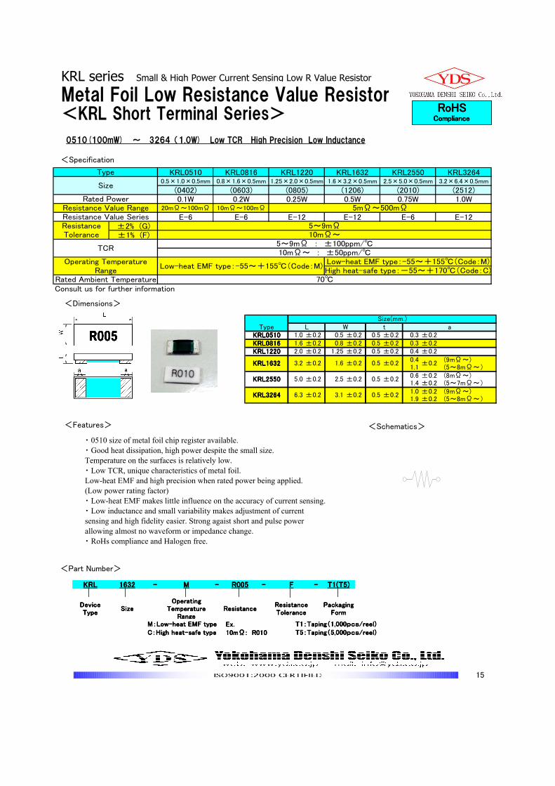
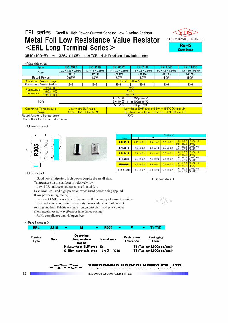
KRL series Small & High Power Current Sensing Low R Value Resistor
RoHSRoHSRoHSRoHSComplianceComplianceComplianceCompliance
Metal Foil Low Resistance Value Resistor<KRL Short Terminal Series>
0510(100mW) ~ 3264(1.0W) Low TCR High Precision Low Inductance
<Specification>
<Dimensions>
TypeKRL0510KRL0510KRL0510KRL0510 1.0 ±0.2 0.5 ±0.2 0.5 ±0.2 0.3 ±0.2KRL0816KRL0816KRL0816KRL0816 1.6 ±0.2 0.8 ±0.2 0.5 ±0.2 0.3 ±0.2KRL1220KRL1220KRL1220KRL1220 2.0 ±0.2 1.25 ±0.2 0.5 ±0.2 0.4 ±0.2
0.4 (9mΩ~)1.1 (5~8mΩ~)0.6 ±0.2 (8mΩ~)1.4 ±0.2 (5~7mΩ~)1.0 ±0.2 (9mΩ~)1.9 ±0.2 (5~8mΩ~)
Size(mm.)L W t a
KRL1632KRL1632KRL1632KRL1632 3.2 ±0.2 1.6 ±0.2 0.5 ±0.2 ±0.2
KRL2550KRL2550KRL2550KRL2550 5.0 ±0.2 2.5 ±0.2 0.5 ±0.2
KRL3264KRL3264KRL3264KRL3264 6.3 ±0.2 3.1 ±0.2 0.5 ±0.2
<Features>
・0510 size of metal foil chip register available.
・Good heat dissipation, high power despite the small size.
Temperature on the surfaces is relatively low.
・Low TCR, unique characteristics of metal foil.
Low-heat EMF and high precision when rated power being applied.
(Low power rating factor)
・Low-heat EMF makes little influence on the accuracy of current sensing.
・Low inductance and small variability makes adjustment of current
sensing and high fidelity easier. Strong agaist short and pulse power
allowing almost no waveform or impedance change.
・RoHs compliance and Halogen free.
<Schematics>
<Part Number>
KRLKRLKRLKRL 1632163216321632 ---- MMMM ---- R005R005R005R005 ---- FFFF ---- T1(T5)T1(T5)T1(T5)T1(T5)
DeviceDeviceDeviceDeviceTypeTypeTypeType
SizeSizeSizeSizeOperatingOperatingOperatingOperating
TemperatureTemperatureTemperatureTemperatureRangeRangeRangeRange
ResistanceResistanceResistanceResistanceResistanceResistanceResistanceResistanceToleranceToleranceToleranceTolerance
PackagingPackagingPackagingPackagingFormFormFormForm
MMMM::::LowLowLowLow----heat EMF typeheat EMF typeheat EMF typeheat EMF type Ex.Ex.Ex.Ex. TTTT1111::::TapingTapingTapingTaping((((1111,,,,000000000000pcspcspcspcs////reelreelreelreel))))CCCC::::High heatHigh heatHigh heatHigh heat----safe typesafe typesafe typesafe type 10101010mmmmΩΩΩΩ:::: RRRR010010010010 TTTT5555::::TapingTapingTapingTaping((((5555,,,,000000000000pcspcspcspcs////reelreelreelreel))))
KRL0510 KRL0816 KRL1220 KRL1632 KRL2550 KRL32640.5×1.0×0.5mm 0.8×1.6×0.5mm 1.25×2.0×0.5mm 1.6×3.2×0.5mm 2.5×5.0×0.5mm 3.2×6.4×0.5mm
(0402) (0603) (0805) (1206) (2010) (2512)0.1W 0.2W 0.25W 0.5W 0.75W 1.0W
20mΩ~100mΩ 10mΩ~100mΩ
E-6 E-6 E-12 E-12 E-6 E-12±2% (G)±1% (F)
Consult us for further information
Type
Size
Rated PowerResistance Value Range 5mΩ~500mΩResistance Value SeriesResistanceTolerance
5~9mΩ10mΩ~
TCR5~9mΩ : ±100ppm/10mΩ~ : ±50ppm/
Operating TemperatureRange
Low-heat EMF type:-55~+155(Code:M)Low-heat EMF type:-55~+155(Code:M)High heat-safe type:-55~+170(Code:C)
Rated Ambient Temperature 70
16
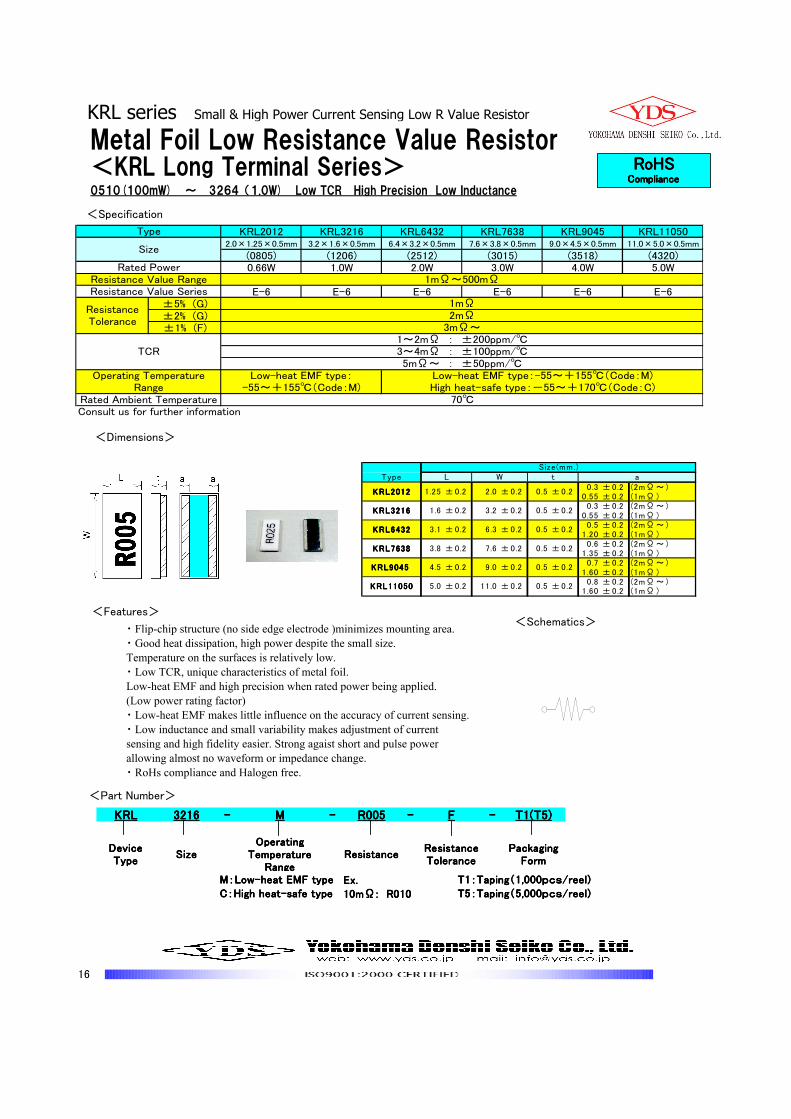
KRL series Small & High Power Current Sensing Low R Value Resistor
RoHSRoHSRoHSRoHSComplianceComplianceComplianceCompliance
Metal Foil Low Resistance Value Resistor<KRL Long Terminal Series>0510(100mW) ~ 3264(1.0W) Low TCR High Precision Low Inductance
<Specification>
<Dimensions>
Type0.3 ± 0.2 (2mΩ ~ )
0.55 ± 0.2 (1mΩ )0.3 ± 0.2 (2mΩ ~ )
0.55 ± 0.2 (1mΩ )0.5 ± 0.2 (2mΩ ~ )
1.20 ± 0.2 (1mΩ )0.6 ± 0.2 (2mΩ ~ )
1.35 ± 0.2 (1mΩ )0.7 ± 0.2 (2mΩ ~ )
1.60 ± 0.2 (1mΩ )0.8 ± 0.2 (2mΩ ~ )
1.60 ± 0.2 (1mΩ )
Size(mm .)L W t a
KRL2012KRL2012KRL2012KRL2012 1.25 ± 0.2 2.0 ± 0.2 0.5 ± 0.2
KRL3216KRL3216KRL3216KRL3216 1.6 ± 0.2 3.2 ± 0.2 0.5 ± 0.2
KRL6432KRL6432KRL6432KRL6432 3.1 ± 0.2 6.3 ± 0.2 0.5 ± 0.2
KRL7638KRL7638KRL7638KRL7638 3.8 ± 0.2 7.6 ± 0.2 0.5 ± 0.2
KRL9045 KRL9045 KRL9045 KRL9045 4.5 ± 0.2 9.0 ± 0.2 0.5 ± 0.2
KRL11050KRL11050KRL11050KRL11050 5.0 ± 0.2 11.0 ± 0.2 0.5 ± 0.2
<Features><Schematics>
<Part Number>
KRLKRLKRLKRL 3216321632163216 ---- MMMM ---- R005R005R005R005 ---- FFFF ---- T1(T5)T1(T5)T1(T5)T1(T5)
DeviceDeviceDeviceDeviceTypeTypeTypeType
SizeSizeSizeSizeOperatingOperatingOperatingOperating
TemperatureTemperatureTemperatureTemperatureRangeRangeRangeRange
ResistanceResistanceResistanceResistanceResistanceResistanceResistanceResistanceToleranceToleranceToleranceTolerance
PackagingPackagingPackagingPackagingFormFormFormForm
MMMM::::LowLowLowLow----heat EMF typeheat EMF typeheat EMF typeheat EMF type Ex.Ex.Ex.Ex. TTTT1111::::TapingTapingTapingTaping((((1111,,,,000000000000pcspcspcspcs////reelreelreelreel))))CCCC::::High heatHigh heatHigh heatHigh heat----safe typesafe typesafe typesafe type 10101010mmmmΩΩΩΩ:::: RRRR010010010010 TTTT5555::::TapingTapingTapingTaping((((5555,,,,000000000000pcspcspcspcs////reelreelreelreel))))
・Flip-chip structure (no side edge electrode )minimizes mounting area.
・Good heat dissipation, high power despite the small size.
Temperature on the surfaces is relatively low.
・Low TCR, unique characteristics of metal foil.
Low-heat EMF and high precision when rated power being applied.
(Low power rating factor)
・Low-heat EMF makes little influence on the accuracy of current sensing.
・Low inductance and small variability makes adjustment of current
sensing and high fidelity easier. Strong agaist short and pulse power
allowing almost no waveform or impedance change.
・RoHs compliance and Halogen free.
KRL2012 KRL3216 KRL6432 KRL7638 KRL9045 KRL110502.0×1.25×0.5mm 3.2×1.6×0.5mm 6.4×3.2×0.5mm 7.6×3.8×0.5mm 9.0×4.5×0.5mm 11.0×5.0×0.5mm
(0805) (1206) (2512) (3015) (3518) (4320)0.66W 1.0W 2.0W 3.0W 4.0W 5.0W
E-6 E-6 E-6 E-6 E-6 E-6±5% (G)±2% (G)±1% (F)
Type
Size
Rated PowerResistance Value Range 1mΩ~500mΩResistance Value Series
ResistanceTolerance
1mΩ2mΩ
3mΩ~
TCR1~2mΩ : ±200ppm/3~4mΩ : ±100ppm/5mΩ~ : ±50ppm/
Operating TemperatureRange
Low-heat EMF type:-55~+155(Code:M)
Low-heat EMF type:-55~+155(Code:M)High heat-safe type:-55~+170(Code:C)
Consult us for further information Rated Ambient Temperature 70
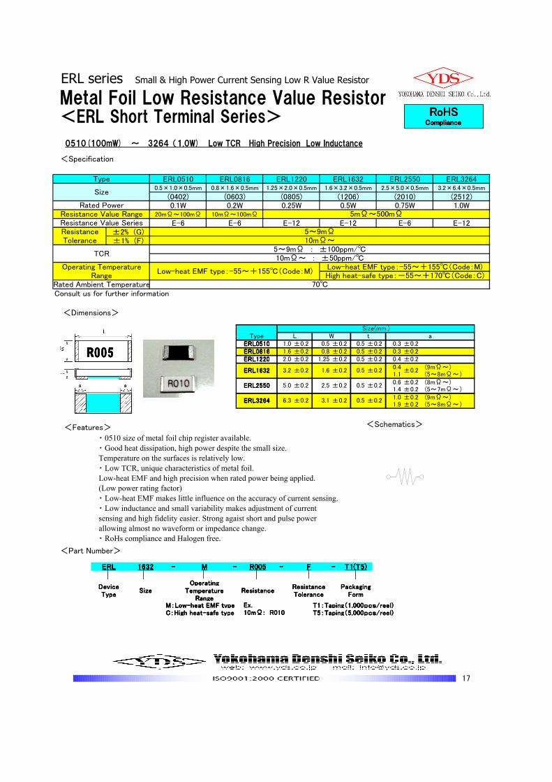
17
<Specification>
<Dimensions>
<Features> <Schematics>
<Part Number>
Metal Foil Low Resistance Value Resistor<ERL Short Terminal Series>
ERL series Small & High Power Current Sensing Low R Value Resistor
0510(100mW) ~ 3264(1.0W) Low TCR High Precision Low Inductance
・0510 size of metal foil chip register available.
・Good heat dissipation, high power despite the small size.
Temperature on the surfaces is relatively low.
・Low TCR, unique characteristics of metal foil.
Low-heat EMF and high precision when rated power being applied.
(Low power rating factor)
・Low-heat EMF makes little influence on the accuracy of current sensing.
・Low inductance and small variability makes adjustment of current
sensing and high fidelity easier. Strong agaist short and pulse power
allowing almost no waveform or impedance change.
・RoHs compliance and Halogen free.
RoHSRoHSRoHSRoHSComplianceComplianceComplianceCompliance
TypeERL0510ERL0510ERL0510ERL0510 1.0 ±0.2 0.5 ±0.2 0.5 ±0.2 0.3 ±0.2ERL0816ERL0816ERL0816ERL0816 1.6 ±0.2 0.8 ±0.2 0.5 ±0.2 0.3 ±0.2ERL1220ERL1220ERL1220ERL1220 2.0 ±0.2 1.25 ±0.2 0.5 ±0.2 0.4 ±0.2
0.4 (9mΩ~)1.1 (5~8mΩ~)0.6 ±0.2 (8mΩ~)1.4 ±0.2 (5~7mΩ~)1.0 ±0.2 (9mΩ~)1.9 ±0.2 (5~8mΩ~)
Size(mm.)L W t a
ERL1632ERL1632ERL1632ERL1632 3.2 ±0.2 1.6 ±0.2 0.5 ±0.2 ±0.2
ERL2550ERL2550ERL2550ERL2550 5.0 ±0.2 2.5 ±0.2 0.5 ±0.2
ERL3264ERL3264ERL3264ERL3264 6.3 ±0.2 3.1 ±0.2 0.5 ±0.2
ERLERLERLERL 1632163216321632 ---- MMMM ---- R005R005R005R005 ---- FFFF ---- T1(T5)T1(T5)T1(T5)T1(T5)
DeviceDeviceDeviceDeviceTypeTypeTypeType
SizeSizeSizeSizeOperatingOperatingOperatingOperating
TemperatureTemperatureTemperatureTemperatureRangeRangeRangeRange
ResistanceResistanceResistanceResistanceResistanceResistanceResistanceResistanceToleranceToleranceToleranceTolerance
PackagingPackagingPackagingPackagingFormFormFormForm
MMMM::::LowLowLowLow----heat EMF typeheat EMF typeheat EMF typeheat EMF type Ex.Ex.Ex.Ex. TTTT1111::::TapingTapingTapingTaping((((1111,,,,000000000000pcspcspcspcs////reelreelreelreel))))CCCC::::High heatHigh heatHigh heatHigh heat----safe typesafe typesafe typesafe type 10101010mmmmΩΩΩΩ:::: RRRR010010010010 TTTT5555::::TapingTapingTapingTaping((((5555,,,,000000000000pcspcspcspcs////reelreelreelreel))))
ERL0510 ERL0816 ERL1220 ERL1632 ERL2550 ERL32640.5×1.0×0.5mm 0.8×1.6×0.5mm 1.25×2.0×0.5mm 1.6×3.2×0.5mm 2.5×5.0×0.5mm 3.2×6.4×0.5mm
(0402) (0603) (0805) (1206) (2010) (2512)0.1W 0.2W 0.25W 0.5W 0.75W 1.0W
20mΩ~100mΩ 10mΩ~100mΩ
E-6 E-6 E-12 E-12 E-6 E-12±2% (G)±1% (F)
Consult us for further information
Type
Size
Rated PowerResistance Value Range 5mΩ~500mΩResistance Value SeriesResistanceTolerance
5~9mΩ10mΩ~
TCR5~9mΩ : ±100ppm/10mΩ~ : ±50ppm/
Operating TemperatureRange
Low-heat EMF type:-55~+155(Code:M)Low-heat EMF type:-55~+155(Code:M)High heat-safe type:-55~+170(Code:C)
Rated Ambient Temperature 70
18
ERL series Small & High Power Current Sensing Low R Value Resistor
RoHSRoHSRoHSRoHSComplianceComplianceComplianceCompliance
Metal Foil Low Resistance Value Resistor<ERL Long Terminal Series>0510(100mW) ~ 3264(1.0W) Low TCR High Precision Low Inductance
<Specification>
<Dimensions>
Type0.3 ±0.2 (2mΩ~)
0.55 ±0.2 (1mΩ)0.3 ±0.2 (2mΩ~)
0.55 ±0.2 (1mΩ)0.5 ±0.2 (2mΩ~)
1.20 ±0.2 (1mΩ)0.6 ±0.2 (2mΩ~)
1.35 ±0.2 (1mΩ)0.7 ±0.2 (2mΩ~)
1.60 ±0.2 (1mΩ)0.8 ±0.2 (2mΩ~)
1.60 ±0.2 (1mΩ)
±0.2 0.5 ±0.2
ERL11050ERL11050ERL11050ERL11050 5.0 ±0.2 11.0 ±0.2 0.5 ±0.2
ERL9045 ERL9045 ERL9045 ERL9045 4.5 ±0.2 9.0
±0.2 0.5 ±0.2
ERL7638ERL7638ERL7638ERL7638 3.8 ±0.2 7.6 ±0.2 0.5 ±0.2
ERL6432ERL6432ERL6432ERL6432 3.1 ±0.2 6.3
±0.2 0.5 ±0.2
ERL3216ERL3216ERL3216ERL3216 1.6 ±0.2 3.2 ±0.2 0.5 ±0.2
ERL2012ERL2012ERL2012ERL2012 1.25 ±0.2 2.0
Size(mm.)L W t a
<Features>
<Schematics>
<Part Number>
ERLERLERLERL 3216321632163216 ---- MMMM ---- R005R005R005R005 ---- FFFF ---- T1(T5)T1(T5)T1(T5)T1(T5)
DeviceDeviceDeviceDeviceTypeTypeTypeType
SizeSizeSizeSizeOperatingOperatingOperatingOperating
TemperatureTemperatureTemperatureTemperatureRangeRangeRangeRange
ResistanceResistanceResistanceResistanceResistanceResistanceResistanceResistanceToleranceToleranceToleranceTolerance
PackagingPackagingPackagingPackagingFormFormFormForm
MMMM::::LowLowLowLow----heat EMF typeheat EMF typeheat EMF typeheat EMF type Ex.Ex.Ex.Ex. TTTT1111::::TapingTapingTapingTaping((((1111,,,,000000000000pcspcspcspcs////reelreelreelreel))))CCCC::::High heatHigh heatHigh heatHigh heat----safe typesafe typesafe typesafe type 10101010mmmmΩΩΩΩ:::: RRRR010010010010 TTTT5555::::TapingTapingTapingTaping((((5555,,,,000000000000pcspcspcspcs////reelreelreelreel))))
・Good heat dissipation, high power despite the small size.
Temperature on the surfaces is relatively low.
・Low TCR, unique characteristics of metal foil.
Low-heat EMF and high precision when rated power being applied.
(Low power rating factor)
・Low-heat EMF makes little influence on the accuracy of current sensing.
・Low inductance and small variability makes adjustment of current
sensing and high fidelity easier. Strong agaist short and pulse power
allowing almost no waveform or impedance change.
・RoHs compliance and Halogen free.
ERL2012 ERL3216 ERL6432 ERL7638 ERL9045 ERL110502.0×1.25×0.5mm 3.2×1.6×0.5mm 6.4×3.2×0.5mm 7.6×3.8×0.5mm 9.0×4.5×0.5mm 11.0×5.0×0.5mm
(0805) (1206) (2512) (3015) (3518) (4320)0.66W 1.0W 2.0W 3.0W 4.0W 5.0W
E-6 E-6 E-6 E-6 E-6 E-6±5% (G)±2% (G)±1% (F)
Type
Size
Rated PowerResistance Value Range 1mΩ~500mΩResistance Value Series
ResistanceTolerance
1mΩ2mΩ
3mΩ~
TCR1~2mΩ : ±200ppm/3~4mΩ : ±100ppm/5mΩ~ : ±50ppm/
Operating TemperatureRange
Low-heat EMF type:-55~+155(Code:M)
Low-heat EMF type:-55~+155(Code:M)High heat-safe type:-55~+170(Code:C)
Consult us for further information Rated Ambient Temperature 70
19
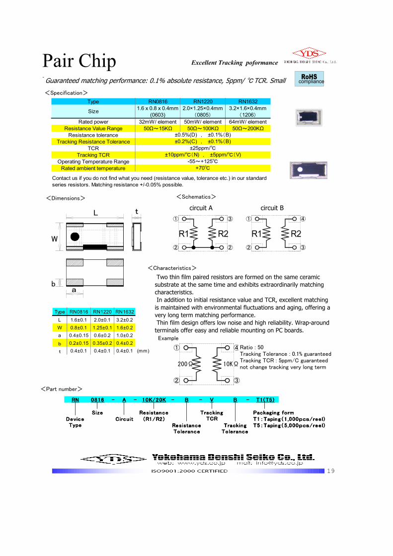
Excellent Tracking poformance
Pair Chip
ResistorGuaranteed matching performance: 0.1% absolute resistance, 5ppm/ TCR. Small
<Specification>
<Dimensions>
<Characteristics>
Two thin film paired resistors are formed on the same ceramic
substrate at the same time and exhibits extraordinarily matching
characteristics.
In addition to initial resistance value and TCR, excellent matching
is maintained with environmental fluctuations and aging, offering a
very long term matching performance.
Thin film design offers low noise and high reliability. Wrap-around
terminals offer easy and reliable mounting on PC boards.
<Schematics>
<Part number>
R1R1
②
R2
② ②
A回路① ③ ①
③
R2
④
B回路
②
200Ω
例)
①
相対抵抗値 0.1%保証相対TCR 5ppm/保証
抵抗比 50倍
③
10KΩ
④
b
W
a
L t
RoHScompliance
Example
Ratio : 50Tracking Tolerance : 0.1% guaranteedTracking TCR : 5ppm/C guaranteednot change tracking very long term
circuit A circuit B
Type RN0816 RN1220 RN1632
L 1.6±0.1 2.0±0.1 3.2±0.2
W 0.8±0.1 1.25±0.1 1.6±0.2
a 0.4±0.15 0.6±0.2 1.0±0.2
b 0.2±0.15 0.35±0.2 0.4±0.2
t 0.4±0.1 0.4±0.1 0.4±0.1 (mm)
RNRNRNRN 0816081608160816 ---- AAAA ---- 10K/20K10K/20K10K/20K10K/20K ---- BBBB ---- VVVV BBBB ---- T1(T5)T1(T5)T1(T5)T1(T5)
SizeSizeSizeSize ResistanceResistanceResistanceResistance Packaging formPackaging formPackaging formPackaging formCircu itCircu itCircu itCircu it (R1/R2)(R1/R2)(R1/R2)(R1/R2) TTTT1111::::TapingTapingTapingTaping((((1111 ,,,,000000000000pcspcspcspcs//// reelreelreelreel))))
TTTT5555::::TapingTapingTapingTaping((((5555 ,,,,000000000000pcspcspcspcs//// reelreelreelreel))))DeviceDeviceDeviceDeviceTypeTypeTypeType
TrackingTrackingTrackingTrackingTCRTCRTCRTCR
ResistanceResistanceResistanceResistanceToleranceToleranceToleranceTolerance
TrackingTrackingTrackingTrackingToleranceToleranceToleranceTolerance
Type RN0816 RN1220 RN1632
1.6 x 0.8 x 0.4mm 2.0×1.25×0.4mm 3.2×1.6×0.4mm
(0603) (0805) (1206)
Rated power 32mW/ element 50mW/ element 64mW/ element
Resistance Value Range 50Ω~15KΩ 50Ω~100KΩ 50Ω~200KΩ
Resistance tolerance
Tracking Resistance Tolerance
TCR
Tracking TCR
Operating Temperature Range
Rated ambient temperature
Size
±0.5%(D) , ±0.1%(B)
±0.2%(C) , ±0.1%(B)
±25ppm/
Contact us if you do not find what you need (resistance value, tolerance etc.) in our standard
series resistors. Matching resistance +/-0.05% possible.
±10ppm/(N) , ±5ppm/(V)
-55~+125
+70
20
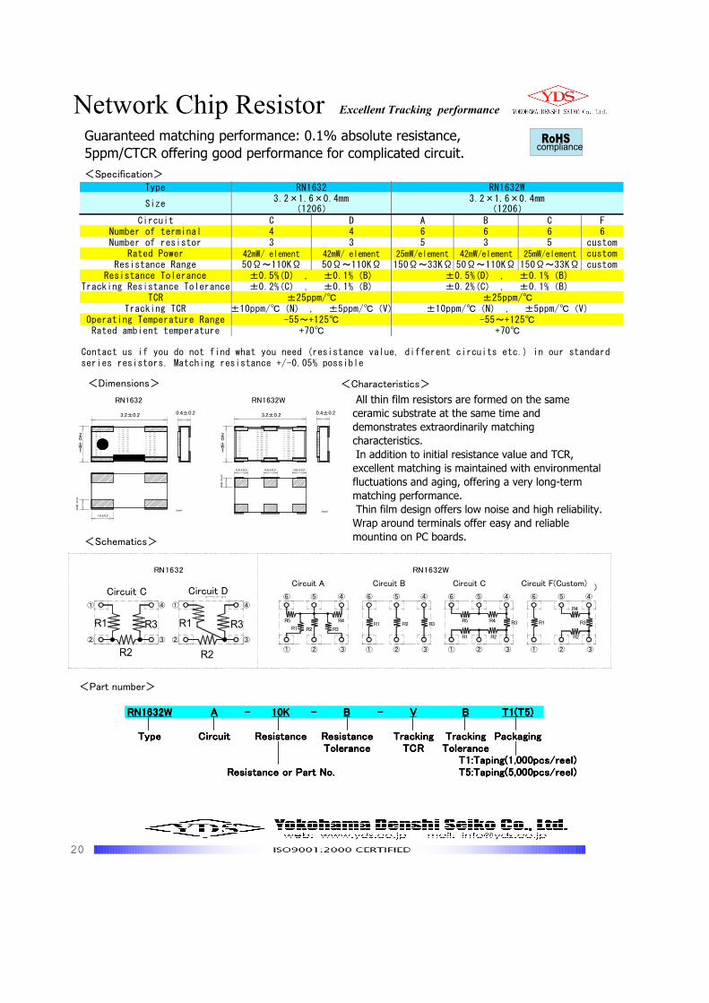
Network Chip Resistor Excellent Tracking performance
Guaranteed matching performance: 0.1% absolute resistance,
5ppm/CTCR offering good performance for complicated circuit.
<Specification>
<Dimensions> <Characteristics>
All thin film resistors are formed on the same
ceramic substrate at the same time and
demonstrates extraordinarily matching
characteristics.
In addition to initial resistance value and TCR,
excellent matching is maintained with environmental
fluctuations and aging, offering a very long-term
matching performance.
Thin film design offers low noise and high reliability.
Wrap around terminals offer easy and reliable
mounting on PC boards.<Schematics>
<Part number>
3.2±0.2 0.4±0.2
1.6
±0.2
0.4
±0.15
1.0±0.2
(mm)
RN1632
0.4±0.2
0.6±0.20.6±0.20.6±0.2
1.6
±0.2
0.4
±0.15
3.2±0.2
(mm)
RN1632W
C回路
R1
②
①
③
④
R1
②
①
③
④
D回路
R2
R3
R2
R3
① ② ③
④⑤⑥
① ② ③
④⑤⑥
① ② ③
④⑤⑥
R1 R2 R3
R4R5R1 R2
R2
R5 R4 R3
R1
R3
B回路 C回路A回路
① ② ③
④⑤⑥
R2
R1
R4
R3
F回路(例:その他)
RN1632 RN1632W
RoHScompliance
Type
Circuit C D A B C FNumber of terminal 4 4 6 6 6 6Number of resistor 3 3 5 3 5 custom
Rated Power 42mW/ element 42mW/ element 25mW/element 42mW/element 25mW/element customResistance Range 50Ω~110KΩ 50Ω~110KΩ 150Ω~33KΩ 50Ω~110KΩ 150Ω~33KΩ custom
Resistance ToleranceTracking Resistance Tolerance
TCRTracking TCR
Operating Temperature RangeRated ambient temperature
Contact us if you do not find what you need (resistance value, different circuits etc.) in our standardseries resistors. Matching resistance +/-0.05% possible
-55~+125+70
RN16323.2×1.6×0.4mm
(1206)
RN1632W3.2×1.6×0.4mm
(1206)
±0.5%(D) , ±0.1%(B)
Size
+70
±0.5%(D) , ±0.1%(B)±0.2%(C) , ±0.1%(B)
±25ppm/±0.2%(C) , ±0.1%(B)
±25ppm/±10ppm/(N) , ±5ppm/(V)
-55~+125±10ppm/(N) , ±5ppm/(V)
Circuit C Circuit DCircuit CCircuit BCircuit A Circuit F(Custom)
RN1632WRN1632WRN1632WRN1632W AAAA ---- 10K10K10K10K ---- BBBB ---- VVVV BBBB T1(T5)T1(T5)T1(T5)T1(T5)
TypeTypeTypeType CircuitCircuitCircuitCircuit ResistanceResistanceResistanceResistance ResistanceResistanceResistanceResistance TrackingTrackingTrackingTracking TrackingTrackingTrackingTracking PackagingPackagingPackagingPackagingToleranceToleranceToleranceTolerance TCRTCRTCRTCR ToleranceToleranceToleranceTolerance
T1:Taping(1,000pcs/reel)T1:Taping(1,000pcs/reel)T1:Taping(1,000pcs/reel)T1:Taping(1,000pcs/reel)Resistance or Part No.Resistance or Part No.Resistance or Part No.Resistance or Part No. T5:Taping(5,000pcs/reel)T5:Taping(5,000pcs/reel)T5:Taping(5,000pcs/reel)T5:Taping(5,000pcs/reel)
21
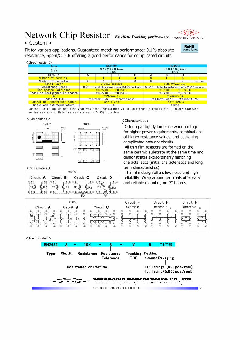
Network Chip Resistor Excellent Tracking performance
< Custom >
Fit for various applications. Guaranteed matching performance: 0.1% absolute
resistance, 5ppm/C TCR offering a good performance for complicated circuits.
<Specification>
<Dimensions> <Characteristics> Offering a slightly larger network package
for higher power requirements, combinations
of higher resistance values, and packaging
complicated network circuits.
All thin film resistors are formed on the
same ceramic substrate at the same time and
demonstrates extraordinarily matching
characteristics (initial characteristics and long
term characteristics)
Thin film design offers low noise and high
reliability. Wrap around terminals offer easy
and reliable mounting on PC boards.
<Schematics>
<Part number>
1.0±0.2
3.2±0.2
(mm)
0.4±0.2
RN2632
2.6±0.2
RN4556
4.5
±0.2
5.6±0.2
(mm)
0.4±0.2
0.4
±0.2
0.4
±0.2
0.6±0.2
②
③
A回路
②
R1
①
R2
② ③
R1
①
R2
B回路④
C回路
R1
②
①
③
④
R2
R3 R1
②
①
③
④
D回路
R3
R2
RN2632
① ②
R1 R2 R3 R4
R5R6
③ ④
⑤⑥⑦⑧
A回路
① ② ③ ④
⑤⑥⑦⑧
B回路
R1 R2 R3 R4
① ② ③ ④
⑤⑥⑦⑧
C回路
RN4556
R1 R3
R4
R5
R2
R6R7
① ② ③ ④
⑤⑥⑦⑧
① ② ③ ④
⑤⑥⑦⑧
① ② ③ ④
⑤⑥⑦⑧
F回路(例) F回路(例) F回路(例)
RoHScompliance
RN2632RN2632RN2632RN2632 AAAA ---- 10K10K10K10K ---- BBBB ---- VVVV BBBB T1(T5)T1(T5)T1(T5)T1(T5)
TypeTypeTypeType Ciucui tCi ucui tCi ucui tCi ucui t ResistanceResistanceResistanceResistance ResistanceResistanceResistanceResistance TrackingTrackingTrackingTracking Track i ngTrack i ngTrack i ngTrack i ng
ToleranceToleranceToleranceTolerance TCRTCRTCRTCR ToleranceTol eranceTol eranceTol erance PakagingPakagingPakagingPakaging
Resistance or Part No.Resistance or Part No.Resistance or Part No.Resistance or Part No. TTTT1111::::TapingTapingTapingTaping((((1111 ,,,,000000000000pcspcspcspcs//// ree lree lree lree l))))TTTT5555::::TapingTapingTapingTaping((((5555 ,,,,000000000000pcspcspcspcs//// ree lree lree lree l))))
Circuit AAAA Circuit BBBB Circuit CCCC
Circuit AAAA Circuit BBBB Circuit CCCC Circuit DDDD
Circuit FFFFexample
Circuit FFFFexample
Circuit FFFFexample
Type
Circuit A B C D A B C FNumber of terminal 3 4 4 4 8 8 8 8Number of resistor 2 2 3 3 6 4 7 custom
Rated PowerResistance Range
Resistance ToleranceTracking Resistance Tolerance
TCRTracking TCR
Operating Temperature RangeRated ambient temperature +70
±0.5%(D) , ±0.1%(B)±0.2%(C) , ±0.1%(B)
±25ppm/±10ppm/(N) , ±5ppm/(V)
-55~+125
RN26323.2×2.6×0.4mm
(1210)
250mW/package
Size
±0.5%(D) , ±0.1%(B)±0.2%(C) , ±0.1%(B)
±25ppm/
50Ω~ Total Resistance max1MΩ/package 50Ω~ Total Resistance max2MΩ/package500mW/package
±10ppm/(N) , ±5ppm/(V)-55~+125
+70
RN45565.6×4.5×0.4mm
(1206)
Contact us if you do not find what you need (resistance value, different circuits etc.) in our standardseries resistors. Matching resistance +/-0.05% possible
22
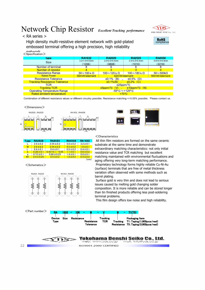
< RA series >
High density multi-resistive element network with gold-plated
embossed terminal offering a high precision, high reliability
network.<Specification>
<Dimensions>
<Characteristics
All thin film resistors are formed on the same ceramic
substrate at the same time and demonstrate
extraordinary matching characteristics: not only initial
resistance value and TCR matching but excellent
matching maintained with environmental fluctuations and
aging offering very long-term matching performance.
Proprietary technology forms highly reliable Cu-Ni-Au
(surface) terminals that are free of metal thickness
variation often observed with some methods such as
barrel plating.
Surface gold is very thin and does not lead to serious
issues caused by melting gold changing solder
composition. It is more reliable and can be stored longer
than tin finished products offering less post-soldering
terminal problems.
This film design offers low noise and high reliability.
<Schematics>
<Part number>
W
RA1632 , RA4556
a
L bt
RA2020 , RA2525
W
W1L
a
btW1
RA1632 , RA4556RA2020 , RA2525
RARARARA 1632163216321632 ---- 10K10K10K10K ---- BBBB ---- VVVV BBBB ---- T1(T5)T1(T5)T1(T5)T1(T5)
SizeSizeSizeSize ResistanceResistanceResistanceResistance Packaging formPackaging formPackaging formPackaging formTCRTCRTCRTCR TrackingTrackingTrackingTracking TTTT1111::::TapingTapingTapingTaping((((1111,,,,000000000000pcspcspcspcs////reelreelreelreel))))
ResistanceResistanceResistanceResistance TTTT5555::::TapingTapingTapingTaping((((5555,,,,000000000000pcspcspcspcs////reelreelreelreel))))
DeviceDeviceDeviceDeviceTypeTypeTypeType ResistanceResistanceResistanceResistance
ToleranceToleranceToleranceTolerance
TrackingTrackingTrackingTracking
RoHScompliance
Network Chip Resistor Excellent Tracking performance
type RA1632 RA2020 RA2525 RA45563.2×1.6×0.5mm 2.0×2.0×0.4mm 2.5×2.5×0.4mm 5.6×4.5×0.8mm
(1206) (0808) (1010) (2218)Number of terminal 8 6 6 8Number of resistor 4 3 3 4Resistance Range 50~100kΩ 100~120kΩ 100~180kΩ 50~500kΩ
Rated Power 30mW/element 50mW/elementResistance Tolerance
Tracking Resistance ToleranceTCR
Tracking TCROperating Temperature Range
Rated ambient temperature
Combination of different resistance values or different circuitry possible. Resistance matching +/-0.05% possible.Please contact us.
-55ºC~+125ºC+70
Size
42mW/element±0.1%(B) 、 ±0.5%(D)±0.1%(B) , ±0.2%(C)
±25ppm/±5ppm/(V) , ±10ppm/(N)
TypeTypeTypeType RA2020RA2020RA2020RA2020 RA2525RA2525RA2525RA2525 RA4556RA4556RA4556RA4556 RA1632RA1632RA1632RA1632L 2.0±0.2 2.54±0.2 5.6±0.2 3.2±0.1W 2.0±0.2 2.54±0.2 4.5±0.2 1.6±0.1t 0.4±0.1 0.4±0.1 0.5±0.2 0.4±0.1b 0.36±0.1 0.43+0.1/-0.05 1.1±0.1 0.6±0.2a 0.72±0.1 0.86±0.25 1.4±0.1 0.8±0.1
W1 0.4±0.25 0.5±0.2 1.0±0.2 0.4±0.2(mm)
23
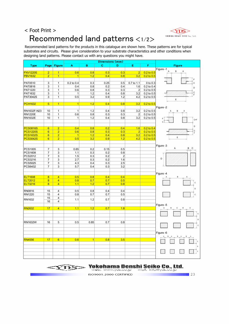
< Foot Print >
Recommended land patterns <1/2> Recommended land patterns for the products in this catalogue are shown here. These patterns are for typical
substrates and circuits. Please give consideration to your substrate characteristics and other conditions when
designing land patterns. Please contact us with any questions you might have.
A B C D E F
Figure -1
PXV1220S 2 1 0.6 0.8 0.3 0.3 2 0.2 to 0.5
PBV1632 2 1 1 1.2 0.4 0.8 3.2 0.2 to 0.5
PAT0510 3 1 0.2 to 0.4 0.3 0.25 0.5 0.7 to 1.1 0 to 0.3
PAT0816 3 1 0.4 0.8 0.2 0.4 1.6 0.2 to 0.4
PAT1220 3 1 0.6 0.8 0.3 0.3 2 0.2 to 0.5
PAT1632 3 1 1 1.2 0.4 0.8 3.2 0.2 to 0.5
PAT3042S 3 1 0.5 3.2 0.9 1.2 4.2 0.2 to 0.5
PCH1632 5 1 1 1.2 0.4 0.8 3.2 0.2 to 0.5
Figure -2
RN1632F-N23 10 1 1 1.2 0.4 0.8 3.2 0.2 to 0.5
RN1220E 10 1 0.6 0.8 0.3 0.3 2 0.2 to 0.5
RN1632E 10 1 1 1.2 0.4 0.8 3.2 0.2 to 0.5
PCS0816S 6 2 0.4 0.8 0.2 0.4 1.6 0.2 to 0.4
PCS1220S 6 2 0.6 0.8 0.3 0.3 2 0.2 to 0.5
PCS1632S 6 2 1 1.2 0.4 0.8 3.2 0.2 to 0.5
PCS3042S 6 2 0.5 3.2 0.9 1.2 4.2 0.2 to 0.5
Figure -3
PCS1005 7 3 0.65 0.2 0.15 0.5
PCS1608 7 3 1.1 0.3 0.2 0.8
PCS2012 7 3 1.5 0.3 0.2 2
PCS3216 7 3 2.7 0.3 0.2 1.6
PCS5025 7 3 4.3 0.4 0.3 2.5
PCS6432 7 3 5.7 0.4 0.3 3.2
Figure -4
ELT1608 8 4 0.5 0.8 0.4 0.4
ELT2012 8 4 0.8 0.7 0.7 0.5
ELT3216 8 4 1.1 1.2 0.7 0.8
RN0816 15 4 0.5 0.8 0.4 0.4
RN1220 15 4 0.8 0.7 0.7 0.5
15 4
16 4
Figure -5
RN2632 17 4 1.1 1.2 0.7 1.8
RN1632W 16 5 0.5 0.85 0.7 0.8
Figure -6
RN4556 17 6 0.6 1 0.8 3.5
0.7
Figure
RN1632 1.1 1.2
Figure
0.8
Dimensions (mm)(mm)(mm)(mm)
Type Page
E
A AB
C
D
F
C
F
E
C
F
A AB
C
D
F
C+F
A
D
B C
A B
C
D
C
A
A AB
C
D
C
AB
C
D
C
AA BBABA
24
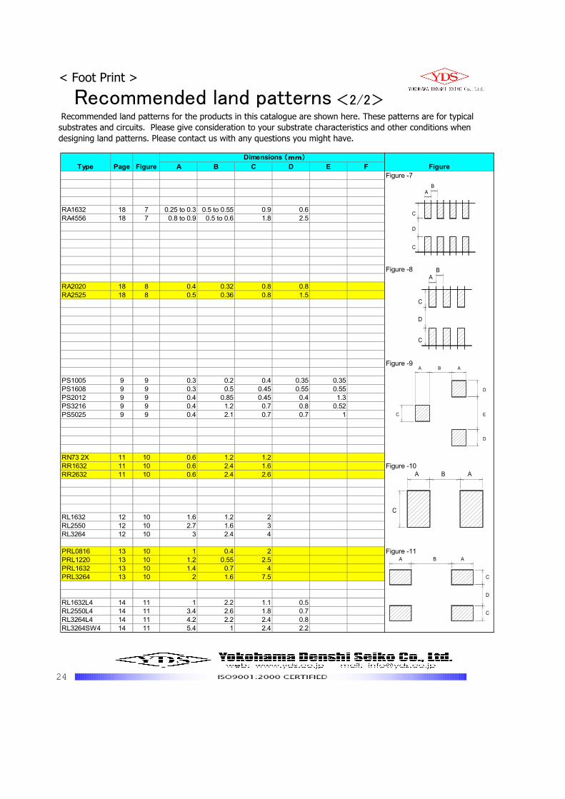
< Foot Print >
Recommended land patterns <2/2> Recommended land patterns for the products in this catalogue are shown here. These patterns are for typical
substrates and circuits. Please give consideration to your substrate characteristics and other conditions when
designing land patterns. Please contact us with any questions you might have.
A B C D E F
Figure -7
RA1632 18 7 0.25 to 0.3 0.5 to 0.55 0.9 0.6
RA4556 18 7 0.8 to 0.9 0.5 to 0.6 1.8 2.5
Figure -8
RA2020 18 8 0.4 0.32 0.8 0.8
RA2525 18 8 0.5 0.36 0.8 1.5
Figure -9
PS1005 9 9 0.3 0.2 0.4 0.35 0.35
PS1608 9 9 0.3 0.5 0.45 0.55 0.55
PS2012 9 9 0.4 0.85 0.45 0.4 1.3
PS3216 9 9 0.4 1.2 0.7 0.8 0.52
PS5025 9 9 0.4 2.1 0.7 0.7 1
RN73 2X 11 10 0.6 1.2 1.2
RR1632 11 10 0.6 2.4 1.6 Figure -10
RR2632 11 10 0.6 2.4 2.6
RL1632 12 10 1.6 1.2 2
RL2550 12 10 2.7 1.6 3
RL3264 12 10 3 2.4 4
PRL0816 13 10 1 0.4 2 Figure -11
PRL1220 13 10 1.2 0.55 2.5
PRL1632 13 10 1.4 0.7 4
PRL3264 13 10 2 1.6 7.5
RL1632L4 14 11 1 2.2 1.1 0.5
RL2550L4 14 11 3.4 2.6 1.8 0.7
RL3264L4 14 11 4.2 2.2 2.4 0.8
RL3264SW4 14 11 5.4 1 2.4 2.2
Type Page Figure
Dimensions (mm)(mm)(mm)(mm)
Figure
AB
C
C
D
BA
C
C
D
A B
C
D
C
A
A AB
C
D
D
E
AB
C
A