Embed Size (px)
Citation preview

Exar Corporation 48720 Kato Road, Fremont CA, 94538 • (510) 668-7000 • FAX (510) 668-7017 • www.exar.com
XRT86VL3xT1/E1/J1 FRAMER/LIU COMBO - ARCHITECTURE DESCRIPTIO N
OCTOBER 2007 REV. 1.2.3
GENERAL DESCRIPTION
The XRT86VL3x is a 1.544 Mbit/s or 2.048 Mbit/sDS1/E1/J1 framer and LIU integrated solution
featuring R3 technology (Relayless, Reconfigurable,Redundancy) that comes in a 2-channel, 4-channel,or 8-channel package. The physical interface isoptimized with internal impedance, and with thepatented pad structure, the XRT86VL3x providesprotection from power failures and hot swapping.
The XRT86VL3x contains an integrated DS1/E1/J1framer and LIU which provide DS1/E1/J1 framing anderror accumulation in accordance with ANSI/ITU_Tspecifications. Each framer has its own framingsynchronizer and transmit-receive slip buffers. Theslip buffers can be independently enabled or disabledas required and can be configured to frame to thecommon DS1/E1/J1 signal formats.
Each Framer block contains its own Transmit andReceive T1/E1/J1 Framing function. There are 3Transmit HDLC controllers per channel whichencapsulate contents of the Transmit HDLC buffersinto LAPD Message frames. There are 3 ReceiveHDLC controllers per channel which extract the
payload content of Receive LAPD Message framesfrom the incoming T1/E1/J1 data stream and write thecontents into the Receive HDLC buffers. Each frameralso contains a Transmit and Overhead Data Inputport, which permits Data Link Terminal Equipmentdirect access to the outbound T1/E1/J1 frames.Likewise, a Receive Overhead output data portpermits Data Link Terminal Equipment direct accessto the Data Link bits of the inbound T1/E1/J1 frames.
The XRT86VL3x fully meets all of the latest T1/E1/J1specifications: ANSI T1/E1.107-1988, ANSI T1/E1.403-1995, ANSI T1/E1.231-1993, ANSI T1/E1.408-1990, AT&T TR 62411 (12-90) TR54016, andITU G-703, G.704, G706 and G.733, AT&T Pub.43801, and ETS 300 011, 300 233, JT G.703, JTG.704, JT G706, I.431. Extensive test and diagnosticfunctions include Loop-backs, Boundary scan,Pseudo Random bit sequence (PRBS) test patterngeneration, Performance Monitor, Bit Error Rate(BER) meter, forced error insertion, and LAPDunchannelized data payload processing according toITU-T standard Q.921.
Applications and Features (next page)
FIGURE 1. XRT86VL3X N-CHANNEL DS1 (T1/E1/J1) FRAMER/LIU COMBO
PerformanceMonitor
PRBSGenerator &
Analyser
HDLC/LAPDControllers
LIU &LoopbackControl
DMAInterfaceSignaling &
AlarmsJTAG
WRALE_ASRDRDY_DTACK
µPSelect
A[14:0]D[7:0]
MicroprocessorInterface
43
Tx SerialClock
Rx SerialClock
8kHz syncOSC
Back Plane1.544-16.384 Mbit/s
Local PCMHighway
ST
-BU
S
2-FrameSlip Buffer
Elastic Store
Tx SerialData In
Tx LIUInterface
2-FrameSlip Buffer
Elastic Store
Rx LIUInterface
Rx FramerRx SerialData Out
RTIP
RRING
TTIP
TRING
External DataLink Controller
Tx Overhead In Rx Overhead OutXRT86VL3x1 of N-channels
Tx Framer
LLB LB
System (Terminal) Side
Line Side
1:1 Turns Ratio
1:2 Turns Ratio
MemoryIntel/Motorola µP
Configuration, Control &Status Monitor
RxLOS
TxON
INT

XRT86VL3X
2
T1/E1/J1 FRAMER/LIU COMBO - ARCHITECTURE DESCRIPTIO N REV. 1.2.3
APPLICATIONS
• High-Density T1/E1/J1 interfaces for Multiplexers,Switches, LAN Routers and Digital Modems
• SONET/SDH terminal or Add/Drop multiplexers(ADMs)
• T1/E1/J1 add/drop multiplexers (MUX)
• Channel Service Units (CSUs): T1/E1/J1 andFractional T1/E1/J1
• Digital Access Cross-connect System (DACs)
• Digital Cross-connect Systems (DCS)
• Frame Relay Switches and Access Devices(FRADS)
• ISDN Primary Rate Interfaces (PRA)
• PBXs and PCM channel bank
• T3 channelized access concentrators and M13MUX
• Wireless base stations
• ATM equipment with integrated DS1 interfaces
• Multichannel DS1 Test Equipment
• T1/E1/J1 Performance Monitoring
• Voice over packet gateways
• Routers
FEATURES
• Independent, full duplex DS1 Tx and Rx Framer/LIUs
• Two 512-bit (two-frame) elastic store, PCM frameslip buffers (FIFO) on TX and Rx provide up to8.192 MHz asynchronous back plane connectionswith jitter and wander attenuation
• Supports input PCM and signaling data at 1.544,2.048, 4.096 and 8.192 Mbits. Also supports 4-channel multiplexed 12.352/16.384 (HMVIP/H.100)Mbit/s on the back plane bus
• Programmable output clocks for Fractional T1/E1/J1
• Supports Channel Associated Signaling (CAS)
• Supports Common Channel Signalling (CCS)
• Supports ISDN Primary Rate Interface (ISDN PRI)signaling
• Extracts and inserts robbed bit signaling (RBS)
• 3 Integrated HDLC controllers per channel fortransmit and receive, each controller having two96-byte buffers (buffer 0 / buffer 1)
• HDLC Controllers Support SS7
• Timeslot assignable HDLC
• V5.1 or V5.2 Interface
• Automatic Performance Report Generation (PMONStatus) can be inserted into the transmit LAPDinterface every 1 second or for a singletransmission
• Alarm Indication Signal with Customer Installationsignature (AIS-CI)
• Remote Alarm Indication with Customer Installation(RAI-CI)
• Gapped Clock interface mode for Transmit andReceive.
• Intel/Motorola and Power PC interfaces forconfiguration, control and status monitoring
• Parallel search algorithm for fast framesynchronization
• Wide choice of T1 framing structures: SF/D4, ESF,SLC®96, T1DM and N-Frame (non-signaling)
• Direct access to D and E channels for fasttransmission of data link information
• PRBS, QRSS, and Network Loop Code generationand detection
• Programmable Interrupt output pin
• Supports programmed I/O and DMA modes ofRead-Write access
• Each framer block encodes and decodes the T1/E1/J1 Frame serial data
• Detects and forces Red (SAI), Yellow (RAI) andBlue (AIS) Alarms
• Detects OOF, LOF, LOS errors and COFAconditions
• Loopbacks: Local (LLB) and Line remote (LB)
• Facilitates Inverse Multiplexing for ATM
• Performance monitor with one second polling
• Boundary scan (IEEE 1149.1) JTAG test port
• Accepts external 8kHz Sync reference
• 1.8V Inner Core Voltage
• 3.3V I/O operation with 5V tolerant inputs

XRT86VL3X
3
REV. 1.2.3 T1/E1/J1 FRAMER/LIU COMBO - ARCHITECTURE DESCRIPTIO N
ORDERING INFORMATION
PART NUMBER PACKAGE OPERATING TEMPERATURE RANGE
XRT86VL38IB 420 Tape Ball Grid Array -40°C to +85°C
XRT86VL38IB484 484 Shrink Thin Ball Grid Array -40°C to +85°C
XRT86VL34IB 225 Plastic Ball Grid Array -40°C to +85°C
XRT86VL32IB 225 Plastic Ball Grid Array -40°C to +85°C
XRT86VL3X
I
T1/E1/J1 FRAMER/LIU COMBO - ARCHITECTURE DESCRIPTIO N REV. 1.2.3
LIST OF PARAGRAPHS
1.0 GENERAL DESCRIPTION AND INTERFACE ............. ............................................................................41.1 PHYSICAL INTERFACE ............................ .......................................................................................................... 41.2 R3 TECHNOLOGY (RELAYLESS / RECONFIGURABLE / RED UNDANCY) .................................................... 5
1.2.1 LINE CARD REDUNDANCY ........................ ................................................................................................................... 51.2.2 TYPICAL REDUNDANCY SCHEMES .................. .......................................................................................................... 51.2.3 1:1 AND 1+1 REDUNDANCY WITHOUT RELAYS ....... ................................................................................................. 51.2.4 TRANSMIT INTERFACE WITH 1:1 AND 1+1 REDUNDANC Y ...................................................................................... 51.2.5 RECEIVE INTERFACE WITH 1:1 AND 1+1 REDUNDANCY ......................................................................................... 6
1.3 POWER FAILURE PROTECTION ...................... ................................................................................................. 71.4 OVERVOLTAGE AND OVERCURRENT PROTECTION ........ ............................................................................ 71.5 NON-INTRUSIVE MONITORING ......................................................................................................................... 71.6 T1/E1 SERIAL PCM INTERFACE .................... ................................................................................................... 81.7 T1/E1 FRACTIONAL INTERFACE .................... .................................................................................................. 91.8 T1/E1 TIME SLOT SUBSTITUTION AND CONTROL ...... ................................................................................. 101.9 ROBBED BIT SIGNALING/CAS SIGNALING ............ ....................................................................................... 111.10 OVERHEAD INTERFACE ........................... ..................................................................................................... 121.11 FRAMER BYPASS MODE ........................... .................................................................................................... 141.12 HIGH-SPEED NON-MULTIPLEXED INTERFACE ......... ................................................................................. 151.13 HIGH-SPEED MULTIPLEXED INTERFACE ............. ...................................................................................... 16
2.0 LOOPBACK MODES OF OPERATION ................... ..............................................................................172.1 LIU PHYSICAL INTERFACE LOOPBACK DIAGNOSTICS ... ........................................................................... 17
2.1.1 LOCAL ANALOG LOOPBACK ....................... ............................................................................................................. 172.1.2 REMOTE LOOPBACK ............................. ..................................................................................................................... 172.1.3 DIGITAL LOOPBACK ............................ ....................................................................................................................... 182.1.4 DUAL LOOPBACK ............................... ........................................................................................................................ 182.1.5 FRAMER REMOTE LINE LOOPBACK ................. ....................................................................................................... 192.1.6 FRAMER LOCAL LOOPBACK ....................... .............................................................................................................. 19
3.0 HDLC CONTROLLERS AND LAPD MESSAGES ............ .....................................................................203.1 STORING AND RETRIEVING MESSAGE CONTENTS ....... ............................................................................. 213.2 PROGRAMMING SEQUENCE FOR SENDING HDLC MESSAGES ................................................................ 223.3 PROGRAMMING SEQUENCE FOR RECEIVING LAPD MESSAGE S ............................................................. 233.4 RECEIVE HDLC EVENT TIMING ...................................................................................................................... 243.5 SS7 (SIGNALING SYSTEM NUMBER 7) FOR ESF IN DS1 ONLY .................................................................. 243.6 DS1/E1 DATALINK TRANSMISSION USING THE HDLC CON TROLLERS .......................................... ......... 253.7 TRANSMIT BOS (BIT ORIENTED SIGNALING) PROCESSOR ....................................................................... 25
3.7.1 DESCRIPTION OF BOS ................................................................................................................................................ 253.7.2 PRIORITY CODEWORD MESSAGE ............................................................................................................................ 253.7.3 COMMAND AND RESPONSE INFORMATION ............ ................................................................................................ 25
3.8 TRANSMIT MOS (MESSAGE ORIENTED SIGNALING) PROCE SSOR .......................................................... 263.8.1 DISCUSSION OF MOS ................................................................................................................................................. 263.8.2 PERIODIC PERFORMANCE REPORT ........................................................................................................................ 273.8.3 TRANSMISSION-ERROR EVENT ................................................................................................................................ 273.8.4 PATH AND TEST SIGNAL IDENTIFICATION MESSAGE . .......................................................................................... 283.8.5 FRAME STRUCTURE ................................................................................................................................................... 283.8.6 FLAG SEQUENCE ............................... ......................................................................................................................... 283.8.7 ADDRESS FIELD ............................... ........................................................................................................................... 283.8.8 ADDRESS FIELD EXTENSION BIT (EA) ............ ......................................................................................................... 283.8.9 COMMAND OR RESPONSE BIT (C/R) ............... ......................................................................................................... 283.8.10 SERVICE ACCESS POINT IDENTIFIER (SAPI) ..... ................................................................................................... 293.8.11 TERMINAL ENDPOINT IDENTIFIER (TEI) ......... ........................................................................................................ 293.8.12 CONTROL FIELD .............................. .......................................................................................................................... 293.8.13 FRAME CHECK SEQUENCE (FCS) FIELD ........... .................................................................................................... 293.8.14 TRANSPARENCY (ZERO STUFFING) ............... ........................................................................................................ 29
3.9 TRANSMIT SLC®96 DATA LINK CONTROLLER .......... .................................................................................. 303.10 D/E TIME SLOT TRANSMIT HDLC CONTROLLER BLOCK V 5.1 OR V5.2 INTERFACE ............................ 313.11 AUTOMATIC PERFORMANCE REPORT (APR) ........... ................................................................................. 31
3.11.1 BIT VALUE INTERPRETATION ................... .............................................................................................................. 314.0 OVERHEAD INTERFACE BLOCK ...................... ..................................................................................33
4.1 DS1 TRANSMIT OVERHEAD INPUT INTERFACE BLOCK ... .......................................................................... 334.1.1 DESCRIPTION OF THE DS1 TRANSMIT OVERHEAD INPUT INTERFACE BLOCK ................................. ............... 33

XRT86VL3X
II
REV. 1.2.3 T1/E1/J1 FRAMER/LIU COMBO - ARCHITECTURE DESCRIPTIO N
4.1.2 CONFIGURE THE DS1 TRANSMIT OVERHEAD INPUT INTERFACE MODULE AS SOURCE OF THE FACILITY DATA LINK (FDL) BITS IN ESF FRAMING FORMAT MODE ........ ......................................................................................... 33
4.1.3 CONFIGURE THE DS1 TRANSMIT OVERHEAD INPUT INTERFACE MODULE AS SOURCE OF THE SIGNALING FRAMING (FS) BITS IN N OR SLC®96 FRAMING FORMAT MOD E .......................................................................... 35
4.1.4 CONFIGURE THE DS1 TRANSMIT OVERHEAD INPUT INTERFACE MODULE AS SOURCE OF THE REMOTE SIG-NALING (R) BITS IN T1DM FRAMING FORMAT MODE ....... ...................................................................................... 36
4.2 DS1 RECEIVE OVERHEAD OUTPUT INTERFACE BLOCK ... ........................................................................ 374.2.1 DESCRIPTION OF THE DS1 RECEIVE OVERHEAD OUTPUT INTERFACE BLOCK ................................. .............. 374.2.2 CONFIGURE THE DS1 RECEIVE OVERHEAD OUTPUT INTERFACE MODULE AS DESTINATION OF THE FACILITY
DATA LINK (FDL) BITS IN ESF FRAMING FORMAT MODE ... ................................................................................... 374.2.3 CONFIGURE THE DS1 RECEIVE OVERHEAD OUTPUT INTERFACE MODULE AS DESTINATION OF THE SIGNALING
FRAMING (FS) BITS IN N OR SLC®96 FRAMING FORMAT MOD E .......................................................................... 394.2.4 CONFIGURE THE DS1 RECEIVE OVERHEAD OUTPUT INTERFACE MODULE AS DESTINATION OF THE REMOTE
SIGNALING (R) BITS IN T1DM FRAMING FORMAT MODE .... ................................................................................... 404.3 E1 OVERHEAD INTERFACE BLOCK ................... ........................................................................................... 414.4 E1 TRANSMIT OVERHEAD INPUT INTERFACE BLOCK .... ........................................................................... 41
4.4.1 DESCRIPTION OF THE E1 TRANSMIT OVERHEAD INPUT INTERFACE BLOCK .................................. ................. 414.4.2 CONFIGURE THE E1 TRANSMIT OVERHEAD INPUT INTERFACE MODULE AS SOURCE OF THE NATIONAL BIT SE-
QUENCE IN E1 FRAMING FORMAT MODE .................. .............................................................................................. 424.5 E1 RECEIVE OVERHEAD INTERFACE ................. .......................................................................................... 45
4.5.1 DESCRIPTION OF THE E1 RECEIVE OVERHEAD OUTPUT INTERFACE BLOCK .................................. ............... 454.5.2 CONFIGURE THE E1 RECEIVE OVERHEAD OUTPUT INTERFACE MODULE AS SOURCE OF THE NATIONAL BIT
SEQUENCE IN E1 FRAMING FORMAT MODE ................ ............................................................................................ 455.0 LIU TRANSMIT PATH ............................. .............................................................................................. 47
5.1 TRANSMIT DIAGNOSTIC FEATURES .................. ........................................................................................... 475.1.1 TAOS (TRANSMIT ALL ONES) .................... ................................................................................................................ 475.1.2 ATAOS (AUTOMATIC TRANSMIT ALL ONES) ......... .................................................................................................. 475.1.3 NETWORK LOOP UP CODE ........................ ................................................................................................................ 475.1.4 NETWORK LOOP DOWN CODE ...................... ........................................................................................................... 485.1.5 QRSS GENERATION .................................................................................................................................................... 48
5.2 T1 LONG HAUL LINE BUILD OUT (LBO) ............. ........................................................................................... 485.3 T1 SHORT HAUL LINE BUILD OUT (LBO) ............ .......................................................................................... 51
5.3.1 ARBITRARY PULSE GENERATOR ................... .......................................................................................................... 515.3.2 DMO (DIGITAL MONITOR OUTPUT) ................ ........................................................................................................... 525.3.3 TRANSMIT JITTER ATTENUATOR .................. ........................................................................................................... 52
5.4 LINE TERMINATION (TTIP/TRING) ................. ................................................................................................. 526.0 LIU RECEIVE PATH .............................. ................................................................................................ 53
6.1 LINE TERMINATION (RTIP/RRING) ................. ................................................................................................ 536.1.1 INTERNAL TERMINATION ........................ ................................................................................................................... 536.1.2 EQUALIZER CONTROL ........................... .................................................................................................................... 536.1.3 CABLE LOSS INDICATOR ........................ ................................................................................................................... 54
6.2 RECEIVE SENSITIVITY ..................................................................................................................................... 546.2.1 AIS (ALARM INDICATION SIGNAL) ............... ............................................................................................................. 556.2.2 NLCD (NETWORK LOOP CODE DETECTION) .......... ................................................................................................. 556.2.3 FLSD (FIFO LIMIT STATUS DETECTION) .......... ........................................................................................................ 566.2.4 RECEIVE JITTER ATTENUATOR ................... ............................................................................................................. 566.2.5 RXMUTE (RECEIVER LOS WITH DATA MUTING) ...... ............................................................................................... 56
7.0 THE E1 TRANSMIT/RECEIVE FRAMER ................ .............................................................................. 587.1 DESCRIPTION OF THE TRANSMIT/RECEIVE PAYLOAD DAT A INPUT INTERFACE BLOCK .................... 58
7.1.1 BRIEF DISCUSSION OF THE TRANSMIT/RECEIVE PAYL OAD DATA INPUT INTERFACE BLOCK OPERATING AT XRT84V24 COMPATIBLE 2.048MBIT/S MODE .............. ............................................................................................. 58
7.2 TRANSMIT/RECEIVE HIGH-SPEED BACK-PLANE INTERFAC E .................................................................. 607.2.1 NON-MULTIPLEXED HIGH-SPEED MODE ............. .................................................................................................... 607.2.2 MULTIPLEXED HIGH-SPEED MODE ................. ......................................................................................................... 63
7.3 BRIEF DISCUSSION OF COMMON CHANNEL SIGNALING IN E1 FRAMING FORMAT .............................. 697.4 BRIEF DISCUSSION OF CHANNEL ASSOCIATED SIGNALIN G IN E1 FRAMING FORMAT ....................... 697.5 INSERT/EXTRACT SIGNALING BITS FROM TSCR REGISTE R .................................................................... 697.6 INSERT/EXTRACT SIGNALING BITS FROM TXCHN[0]_N/T XSIG PIN ......................................................... 697.7 ENABLE CHANNEL ASSOCIATED SIGNALING AND SIGNALI NG DATA SOURCE CONTROL ................. 70
8.0 THE DS1 TRANSMIT/RECEIVE FRAMER ............... ............................................................................. 718.1 DESCRIPTION OF THE TRANSMIT/RECEIVE PAYLOAD DAT A INPUT INTERFACE BLOCK .................... 71
8.1.1 BRIEF DISCUSSION OF THE TRANSMIT/RECEIVE PAYL OAD DATA INPUT INTERFACE BLOCK OPERATING AT 1.544MBIT/S MODE ....................................................................................................................................................... 71
8.2 TRANSMIT/RECEIVE HIGH-SPEED BACK-PLANE INTERFAC E .................................................................. 73

XRT86VL3X
III
T1/E1/J1 FRAMER/LIU COMBO - ARCHITECTURE DESCRIPTIO N REV. 1.2.3
8.2.1 T1 TRANSMIT/RECEIVE INTERFACE - MVIP 2.048 MHZ .......................................................................................... 738.2.2 NON-MULTIPLEXED HIGH-SPEED MODE ............. .................................................................................................... 748.2.3 MULTIPLEXED HIGH-SPEED MODE ................. ......................................................................................................... 76
8.3 BRIEF DISCUSSION OF ROBBED-BIT SIGNALING IN DS1 FRAMING FORMAT ................................... ..... 858.3.1 CONFIGURE THE FRAMER TO TRANSMIT ROBBED-BIT S IGNALING .......................................... ......................... 868.3.2 INSERT SIGNALING BITS FROM TSCR REGISTER .... .............................................................................................. 868.3.3 INSERT SIGNALING BITS FROM TXSIG_N PIN ...... ................................................................................................... 87
9.0 ALARMS AND ERROR CONDITIONS ................... ...............................................................................899.1 AIS ALARM ..................................... ................................................................................................................... 899.2 RED ALARM ..................................... ................................................................................................................. 919.3 YELLOW ALARM .................................. ............................................................................................................ 929.4 BIPOLAR VIOLATION ............................. .......................................................................................................... 949.5 E1 BRIEF DISCUSSION OF ALARMS AND ERROR CONDITI ONS ............................................................... 96
9.5.1 HOW TO CONFIGURE THE FRAMER TO TRANSMIT AIS . ..................................................................................... 1029.5.2 HOW TO CONFIGURE THE FRAMER TO GENERATE RED A LARM .............................................. ....................... 1039.5.3 HOW TO CONFIGURE THE FRAMER TO TRANSMIT YELLO W ALARM ........................................... .................... 1039.5.4 TRANSMIT YELLOW ALARM ....................... ............................................................................................................. 1049.5.5 TRANSMIT CAS MULTI-FRAME YELLOW ALARM ....... .......................................................................................... 104
9.6 T1 BRIEF DISCUSSION OF ALARMS AND ERROR CONDITI ONS .............................................................. 1059.6.1 HOW TO CONFIGURE THE FRAMER TO TRANSMIT AIS . ..................................................................................... 1089.6.2 HOW TO CONFIGURE THE FRAMER TO GENERATE RED A LARM .............................................. ....................... 1099.6.3 HOW TO CONFIGURE THE FRAMER TO TRANSMIT YELLO W ALARM ........................................... .................... 1099.6.4 TRANSMIT YELLOW ALARM IN SF MODE ............ .................................................................................................. 1109.6.5 TRANSMIT YELLOW ALARM IN ESF MODE ........... ................................................................................................. 1109.6.6 TRANSMIT YELLOW ALARM IN N MODE ............. ................................................................................................... 1109.6.7 TRANSMIT YELLOW ALARM IN T1DM MODE .......... ............................................................................................... 110
10.0 APPENDIX A: DS-1/E1 FRAMING FORMATS .......... ........................................................................11210.1 THE E1 FRAMING STRUCTURE .................................................................................................................. 112
10.1.1 FAS FRAME .................................. ............................................................................................................................ 11210.1.2 NON-FAS FRAME .............................. ....................................................................................................................... 113
10.2 THE E1 MULTI-FRAME STRUCTURE ................. ......................................................................................... 11410.2.1 THE CRC MULTI-FRAME STRUCTURE .............. .................................................................................................... 11410.2.2 CAS MULTI-FRAMES AND CHANNEL ASSOCIATED SIGN ALING ............................................. ......................... 115
10.3 THE DS1 FRAMING STRUCTURE ................................................................................................................ 11710.4 T1 SUPER FRAME FORMAT (SF) ................... ............................................................................................. 11810.5 T1 EXTENDED SUPERFRAME FORMAT (ESF) .......... ................................................................................ 11910.6 T1 NON-SIGNALING FRAME FORMAT ................ ....................................................................................... 12110.7 T1 DATA MULTIPLEXED FRAMING FORMAT (T1DM) .... ........................................................................... 12110.8 SLC-96 FORMAT (SLC-96) ....................... .................................................................................................... 12210.9 DMA WRITE CYCLE TIMING ....................... ................................................................................................. 14210.10 DMA READ CYCLE TIMING ....................... ................................................................................................. 142

XRT86VL3X
IV
REV. 1.2.3 T1/E1/J1 FRAMER/LIU COMBO - ARCHITECTURE DESCRIPTIO N
LIST OF FIGURES
Figure 1.: XRT86VL3x N-Channel DS1 (T1/E1/J1) Framer/LIU Combo ........................................................................... 1Figure 2.: LIU Transmit Connection Diagram Using Internal Termination ......................................................................... 4Figure 3.: LIU Receive Connection Diagram Using Internal Termination ......................................................................... 4Figure 4.: Simplified Block Diagram of the Transmit Interface for 1:1 and 1+1 Redundancy ............................................ 5Figure 5.: Simplified Block Diagram of the Receive Interface for 1:1 and 1+1 Redundancy ............................................. 6Figure 6.: Simplified Block Diagram of a Non-Intrusive Monitoring Application ................................................................. 7Figure 7.: Transmit T1/E1 Serial PCM Interface ................................................................................................................ 8Figure 8.: Receive T1/E1 Serial PCM Interface ................................................................................................................. 8Figure 9.: T1 Fractional Interface ....................................................................................................................................... 9Figure 10.: T1/E1 Time Slot Substitution and Control ..................................................................................................... 10Figure 11.: Robbed Bit Signaling / CAS Signaling ........................................................................................................... 11Figure 12.: ESF / CAS External Signaling Bus ................................................................................................................ 11Figure 13.: SF / SLC-96 or 4-code Signaling in ESF / CAS External Signaling Bus ....................................................... 12Figure 14.: T1/E1 Overhead Interface ............................................................................................................................. 12Figure 15.: T1 External Overhead Datalink Bus .............................................................................................................. 13Figure 16.: E1 Overhead External Datalink Bus .............................................................................................................. 13Figure 17.: Simplified Block Diagram of the Framer Bypass Mode ................................................................................. 14Figure 18.: T1 High-Speed Non-Multiplexed Interface .................................................................................................... 15Figure 19.: E1 High-Speed Non-Multiplexed Interface .................................................................................................... 15Figure 20.: Transmit High-Speed Bit Multiplexed Block Diagram .................................................................................... 16Figure 21.: Receive High-Speed Bit Multiplexed Block Diagram ..................................................................................... 16Figure 22.: Simplified Block Diagram of Local Analog Loopback .................................................................................... 17Figure 23.: Simplified Block Diagram of Remote Loopback ............................................................................................ 17Figure 24.: Simplified Block Diagram of Digital Loopback ............................................................................................... 18Figure 25.: Simplified Block Diagram of Dual Loopback .................................................................................................. 18Figure 26.: Simplified Block Diagram of the Framer Remote Line Loopback .................................................................. 19Figure 27.: Simplified Block Diagram of the Framer Local Loopback .............................................................................. 19Figure 28.: HDLC Controllers .......................................................................................................................................... 20Figure 29.: Storing and Retrieving Message Contents .................................................................................................... 21Figure 30.: Sending HDLC Messages ............................................................................................................................. 22Figure 31.: Receiving HDLC Messages ........................................................................................................................... 23Figure 32.: Receive HDLC Event Timing ......................................................................................................................... 24Figure 33.: LAPD Frame Structure .................................................................................................................................. 27Figure 34.: Block Diagram of the DS1 Transmit Overhead Input Interface of the XRT86VL3x ....................................... 33Figure 35.: DS1 Transmit Overhead Input Interface Timing in ESF Framing Format mode ............................................ 35Figure 36.: DS1 Transmit Overhead Input Timing in N or SLC®96 Framing Format Mode ............................................ 36Figure 37.: DS1 Transmit Overhead Input Interface module in T1DM Framing Format mode ........................................ 36Figure 38.: Block Diagram of the DS1 Receive Overhead Output Interface of XRT86VL3x ........................................... 37Figure 39.: DS1 Receive Overhead Output Interface module in ESF framing format mode ........................................... 39Figure 40.: DS1 Receive Overhead Output Interface Timing in N or SLC®96 Framing Format mode ........................... 40Figure 41.: DS1 Receive Overhead Output Interface Timing in T1DM Framing Format mode ....................................... 41Figure 42.: Block Diagram of the E1 Transmit Overhead Input Interface of XRT86VL3x ................................................ 42Figure 43.: E1 Transmit Overhead Input Interface Timing ............................................................................................... 44Figure 44.: Block Diagram of the E1 Receive Overhead Output Interface of XRT86VL3x .............................................. 45Figure 45.: E1 Receive Overhead Output Interface Timing ............................................................................................. 46Figure 46.: TAOS (Transmit All Ones) ............................................................................................................................. 47Figure 47.: Simplified Block Diagram of the ATAOS Function ......................................................................................... 47Figure 48.: Network Loop Up Code Generation .............................................................................................................. 48Figure 49.: Network Loop Down Code Generation .......................................................................................................... 48Figure 50.: Long Haul Line Build Out with -7.5dB Attenuation ........................................................................................ 49Figure 51.: Long Haul Line Build Out with -15dB Attenuation ......................................................................................... 49Figure 52.: Long Haul Line Build Out with -22.5dB Attenuation ...................................................................................... 50Figure 53.: Arbitrary Pulse Segment Assignment ............................................................................................................ 51Figure 54.: Typical Connection Diagram Using Internal Termination .............................................................................. 52Figure 55.: Typical Connection Diagram Using Internal Termination ............................................................................. 53Figure 56.: Simplified Block Diagram of the Equalizer and Peak Detector ...................................................................... 54Figure 57.: Simplified Block Diagram of the Cable Loss Indicator ................................................................................... 54Figure 58.: Test Configuration for Measuring Receive Sensitivity ................................................................................... 55

XRT86VL3X
V
T1/E1/J1 FRAMER/LIU COMBO - ARCHITECTURE DESCRIPTIO N REV. 1.2.3
Figure 59.: Process Block for Automatic Loop Code Detection ....................................................................................... 56Figure 60.: Simplified Block Diagram of the RxMUTE Function ...................................................................................... 57Figure 61.: Interfacing the Transmit Path to local terminal equipment ............................................................................. 58Figure 63.: Waveforms for connecting the Transmit Payload Data Input Interface Block to local Terminal Equipment .. 59Figure 62.: Interfacing the Receive Path to local terminal equipment .............................................................................. 59Figure 64.: Waveforms for connecting the Receive Payload Data Input Interface Block to local Terminal Equipment ... 60Figure 65.: Transmit Non-Multiplexed High-Speed Connection to local terminal equipment using MVIP 2.048Mbit/s,
4.096Mbit/s, or 8.192Mbit/s ............................................................................................................................... 61Figure 66.: Receive Non-Multiplexed High-Speed Connection to local terminal equipment using MVIP 2.048Mbit/s,
4.096Mbit/s, or 8.192Mbit/s ............................................................................................................................... 61Figure 67.: Waveforms for Connecting the Transmit Non-Multiplexed High-Speed Input Interface at MVIP 2.048Mbit/s,
4.096Mbit/s, and 8.192Mbit/s ............................................................................................................................ 62Figure 68.: Waveforms for Connecting the Receive Non-Multiplexed High-Speed Input Interface at MVIP 2.048Mbit/s,
4.096Mbit/s, and 8.192Mbit/s ............................................................................................................................ 62Figure 69.: Interfacing XRT86VL3x Transmit to local terminal equipment using 16.384Mbit/s, HMVIP 16.384Mbit/s, and
H.100 16.384Mbit/s ........................................................................................................................................... 66Figure 70.: Timing signal when the framer is running at Bit-Multiplexed 16.384Mbit/s mode .......................................... 66Figure 71.: Waveforms for Connecting the Transmit Multiplexed High-Speed Input Interface at HMVIP And H.100
16.384Mbit/s mode ............................................................................................................................................ 67Figure 72.: Interfacing XRT86VL3x Receive to local terminal equipment using 16.384Mbit/s, HMVIP 16.384Mbit/s, and
H.100 16.384Mbit/s ........................................................................................................................................... 68Figure 73.: Timing Signal When the Receive Framer is running at 16.384MHz Bit-Mulitplexed Mode ........................... 68Figure 74.: Timing Signal wehn the Receive Framer is Running at HMVIP and H100 16.384MHz Mode ...................... 68Figure 75.: Timing Diagram of the TxSIG Input ............................................................................................................... 70Figure 76.: Timing Diagram of the RxSIG Output ............................................................................................................ 70Figure 77.: Interfacing the Transmit Path to local terminal equipment ............................................................................. 71Figure 79.: Waveforms for connecting the Transmit Payload Data Input Interface Block to local Terminal Equipment .. 72Figure 78.: Interfacing the Receive Path to local terminal equipment .............................................................................. 72Figure 80.: Waveforms for connecting the Receive Payload Data Input Interface Block to local Terminal Equipment ... 73Figure 81.: Transmit Non-Multiplexed High-Speed Connection to local terminal equipment using MVIP 2.048Mbit/s,
4.096Mbit/s, or 8.192Mbit/s ............................................................................................................................... 74Figure 83.: Waveforms for Connecting the Transmit Non-Multiplexed High-Speed Input Interface at MVIP 2.048Mbit/s,
4.096Mbit/s, and 8.192Mbit/s ............................................................................................................................ 75Figure 82.: Receive Non-Multiplexed High-Speed Connection to local terminal equipment using MVIP 2.048Mbit/s,
4.096Mbit/s, or 8.192Mbit/s ............................................................................................................................... 75Figure 84.: Waveforms for Connecting the Receive Non-Multiplexed High-Speed Input Interface at MVIP 2.048Mbit/s,
4.096Mbit/s, and 8.192Mbit/s ............................................................................................................................ 76Figure 85.: Interfacing XRT86VL3x Transmit to local terminal equipment using 16.384Mbit/s, HMVIP 16.384Mbit/s, and
H.100 16.384Mbit/s ........................................................................................................................................... 78Figure 86.: Timing Signals When the Transmit Framer is Running at 12.352 Bit-Multiplexed Mode ............................... 79Figure 87.: Timing signals when the transmit framer is running at 16.384 Bit-Multiplexed mode .................................... 81Figure 88.: Timing signals when the transmit framer is running at HMVIP / H.100 16.384MHz Mode ............................ 83Figure 89.: Interfacing XRT86VL3x Receive to local terminal equipment using 16.384Mbit/s, HMVIP 16.384Mbit/s, and
H.100 16.384Mbit/s ........................................................................................................................................... 84Figure 90.: Waveforms for Connecting the Receive Multiplexed High-Speed Input Interface at 12.352Mbit/s mode ..... 84Figure 91.: Waveforms for Connecting the Receive Multiplexed High-Speed Input Interface at 16.384Mbit/s mode ..... 84Figure 92.: Waveforms for Connecting the Receive Multiplexed High-Speed Input Interface at HMVIP and H.100 16.384Mbit/
s mode ............................................................................................................................................................... 85Figure 93.: Timing Diagram of the TxSig_n Input ............................................................................................................ 87Figure 94.: Simple Diagram of E1 system model ............................................................................................................. 97Figure 95.: Generation of Yellow Alarm by the Repeater upon detection of line failure .................................................. 98Figure 96.: Generation of AIS by the Repeater upon detection of line failure .................................................................. 99Figure 97.: Generation of Yellow Alarm by the CPE upon detection of AIS originated by the Repeater ....................... 100Figure 98.: Generation of CAS Multi-frame Yellow Alarm and AIS16 by the Repeater ................................................. 101Figure 99.: Generation of CAS Multi-frame Yellow Alarm by the CPE upon detection of “AIS16” pattern sent by the Repeater
102Figure 100.: Simple Diagram of DS1 System Model ..................................................................................................... 105Figure 101.: Generation of Yellow Alarm by the CPE upon detection of line failure ...................................................... 106Figure 102.: Generation of Yellow Alarm by the CPE upon detection of AIS originated by the Repeater ..................... 108Figure 103.: Single E1 Frame Diagram ......................................................................................................................... 112

XRT86VL3X
VI
REV. 1.2.3 T1/E1/J1 FRAMER/LIU COMBO - ARCHITECTURE DESCRIPTIO N
Figure 104.: Frame/Byte Format of the CAS Multi-Frame Structure ............................................................................. 115Figure 105.: E1 Frame Format ...................................................................................................................................... 116Figure 106.: T1 Frame Format ....................................................................................................................................... 117Figure 107.: T1 Superframe PCM Format ..................................................................................................................... 118Figure 108.: T1 Extended Superframe Format .............................................................................................................. 119Figure 109.: T1DM Frame Format ................................................................................................................................. 121Figure 110.: Framer System Transmit Timing Diagram (Base Rate/Non-Mux) ............................................................. 125Figure 111.: Framer System Receive Timing Diagram (RxSERCLK as an Output) ...................................................... 126Figure 112.: Framer System Receive Timing Diagram (RxSERCLK as an Input) ......................................................... 127Figure 113.: Framer System Transmit Timing Diagram (HMVIP and H100 Mode) ....................................................... 128Figure 114.: Framer System Receive Timing Diagram (HMVIP/H100 Mode) ............................................................... 129Figure 115.: Framer System Transmit Overhead Timing Diagram ................................................................................ 130Figure 116.: Framer System Receive Overhead Timing Diagram (RxSERCLK as an Output) ..................................... 131Figure 117.: Framer System Receive Overhead Timing Diagram (RxSERCLK as an Input) ........................................ 131Figure 118.: ITU G.703 Pulse Template ........................................................................................................................ 135Figure 119.: DSX-1 Pulse Template (normalized amplitude) ........................................................................................ 136Figure 120.: Intel µP Interface Timing During Programmed I/O Read and Write Operations When ALE Is Not Tied ’HIGH’
137Figure 121.: Intel µP Interface Timing During Programmed I/O Read and Write Operations When ALE Is Tied ’HIGH’ 139Figure 122.: Motorola Asychronous Mode Interface Signals During Programmed I/O Read and Write Operations ..... 140Figure 123.: Power PC 403 Interface Signals During Programmed I/O Read and Write Operations ........................... 141Figure 124.: DMA Write Cycle Timing Waveform .......................................................................................................... 142Figure 125.: DMA Read Cycle Timing Waveform .......................................................................................................... 142

XRT86VL3X
VII
T1/E1/J1 FRAMER/LIU COMBO - ARCHITECTURE DESCRIPTIO N REV. 1.2.3
LIST OF TABLES
Table 1:: Bit Ordering and Usage .................................................................................................................................... 30Table 2:: Framing Format for PMON Status Inserted within LAPD by Initiating APR ...................................................... 31Table 3:: Random Bit Sequence Polynomials .................................................................................................................. 48Table 4:: Short Haul Line Build Out ................................................................................................................................. 51Table 5:: Selecting the Internal Impedance ..................................................................................................................... 53Table 6:: Mapping a T1 Frame into an E1 Frane ............................................................................................................. 74Table 7:: Bit Format of Timeslot 0 octet within a FAS E1 Frame ................................................................................... 112Table 8:: Bit Format of Timeslot 0 octet within a Non-FAS E1 Frame ........................................................................... 113Table 9:: Bit Format of all Timeslot 0 octets within a CRC Multi-frame .......................................................................... 114Table 10:: Superframe Format ....................................................................................................................................... 118Table 11:: Extended Superframe Format ....................................................................................................................... 120Table 12:: Non-Signaling Framing Format ..................................................................................................................... 121Table 13:: SLC®96 Fs Bit Contents ............................................................................................................................... 122Table 14:: XRT86VL32 Power Consumption ................................................................................................................ 123Table 15:: XRT86VL34 Power Consumption ................................................................................................................ 124Table 16:: XRT86VL38 Power Consumption ................................................................................................................ 124Table 17:: E1 Receiver Electrical Characteristics .......................................................................................................... 132Table 18:: T1 Receiver Electrical Characteristics .......................................................................................................... 133Table 19:: E1 Transmitter Electrical Characteristics ...................................................................................................... 134Table 20:: E1 Transmit Return Loss Requirement ......................................................................................................... 134Table 21:: T1 Transmitter Electrical Characteristics ...................................................................................................... 134Table 22:: Transmit Pulse Mask Specification ............................................................................................................... 135Table 23:: DSX1 Interface Isolated pulse mask and corner points ................................................................................ 136Table 24:: AC Electrical Characteristics ......................................................................................................................... 137Table 25:: Intel Microprocessor Interface Timing Specifications .................................................................................... 137Table 26:: Intel Microprocessor Interface Timing Specifications .................................................................................... 139Table 27:: Motorola Asychronous Mode Microprocessor Interface Timing Specifications ............................................. 140Table 28:: Power PC 403 Microprocessor Interface Timing Specifications ................................................................... 141

XRT86VL3X
4
REV. 1.2.3 T1/E1/J1 FRAMER/LIU COMBO - ARCHITECTURE DESCRIPTIO N
1.0 GENERAL DESCRIPTION AND INTERFACE
The XRT86VL3x supports multiple interfaces for various modes of operation. The purpose of this section is topresent a general overview of the common interfaces and their connection diagrams. Each mode will bedescribed in full detail in later sections of the datasheet.
NOTE: For a brief tutorial on Framing Formats, see Appendix A in the back of this document.
1.1 Physical Interface
The Line Interface Unit generates/receives standard return-to-zero (RZ) signals to the line interface for T1/E1/J1 twisted pair or E1 coaxial cable. The physical interface is optimized by placing the terminating impedanceinside the LIU. This allows one bill of materials for all modes of operation reducing the number of externalcomponents necessary in system design. The transmitter outputs only require one DC blocking capacitor of0.68µF and a 1:2 step-up transformer. The receive path inputs only require one bypass capacitor of 0.1µFconnected to the center tap (CT) of the transformer and a 1:1 transformer. The receive CT bypass capacitor isrequired for Long Haul Applications, and recommended for Short Haul Applications. Figure 2 shows thetypical connection diagram for the LIU transmitters. Figure 3 shows a typical connection diagram for the LIUreceivers.
FIGURE 2. LIU TRANSMIT CONNECTION DIAGRAM USING INTERNAL TERMINATION
FIGURE 3. LIU RECEIVE CONNECTION DIAGRAM USING INTERNAL TERMINATION
TTIP
TRING
XRT86VL3x LIU
1:2
Internal Impedance
Line Interface T1/E1/J1C=0.68uF
One Bill of Materials
TransmitterOutput
RTIP
RRING
XRT86VL3x LIU1:1
Internal Impedance
Line Interface T1/E1/J1
One Bill of Materials
ReceiverInput
0.1µF

XRT86VL3X
5
T1/E1/J1 FRAMER/LIU COMBO - ARCHITECTURE DESCRIPTIO N REV. 1.2.3
1.2 R3 Technology (Relayless / Reconfigurable / Redundanc y)
Redundancy is used to introduce reliability and protection into network card design. The redundant card inmany cases is an exact replicate of the primary card, such that when a failure occurs the network processor
can automatically switch to the backup card. EXAR’s R3 technology has re-defined DS-1/E1/J1 physicalinterface design for 1:1 and 1+1 redundancy applications. Without relays and one Bill of Materials, EXARoffers multi-port, integrated Framer/LIU solutions to assist high density aggregate applications and framing
requirements with reliability. The following section can be used as a reference for implementing R3 Technologywith EXAR’s world leading Framer/LIU combo.
1.2.1 Line Card Redundancy
Telecommunication system design requires signal integrity and reliability. When a T1/E1 primary line card hasa failure, it must be swapped with a backup line card while maintaining connectivity to a backplane withoutlosing data. System designers can achieve this by implementing common redundancy schemes with theXRT86VL3x Framer/LIU. EXAR offers features that are tailored to redundancy applications while reducing thenumber of components and providing system designers with solid reference designs.
1.2.2 Typical Redundancy Schemes
• 1:1 One backup card for every primary card (Facility Protection)
• 1+1 One backup card for every primary card (Line Protection)
• ·N+1 One backup card for N primary cards
1.2.3 1:1 and 1+1 Redundancy Without Relays
The 1:1 facility protection and 1+1 line protection have one backup card for every primary card. When using1:1 or 1+1 redundancy, the backup card has its transmitters tri-stated and its receivers in high impedance. Thiseliminates the need for external relays and provides one bill of materials for all interface modes of operation.For 1+1 line protection, the receiver inputs on the backup card have the ability to monitor the line for bit errorswhile in high impedance. The transmit and receive sections of the physical interface are described separately.
1.2.4 Transmit Interface with 1:1 and 1+1 Redundancy
The transmitters on the backup card should be tri-stated. Select the appropriate impedance for the desiredmode of operation, T1/E1/J1. A 0.68uF capacitor is used in series with TTIP for blocking DC bias. SeeFigure 4 . for a simplified block diagram of the transmit section for a 1:1 and 1+1 redundancy.
FIGURE 4. SIMPLIFIED BLOCK DIAGRAM OF THE TRANSMIT INTERFACE FOR 1:1 AND 1+1 REDUNDANCY
T1/E1 Line
Backplane Interface
Primary Card
Backup Card
XRT86VL3x
Tx
Tx 0.68uF
0.68uF
Internal Impedence
1:2
1:2
XRT86VL3x
Internal Impedence

XRT86VL3X
6
REV. 1.2.3 T1/E1/J1 FRAMER/LIU COMBO - ARCHITECTURE DESCRIPTIO N
1.2.5 Receive Interface with 1:1 and 1+1 Redundancy
The receivers on the backup card should be programmed for "High" impedance. Since there is no externalresistor in the circuit, the receivers on the backup card will not load down the line interface. This key designfeature eliminates the need for relays and provides one bill of materials for all interface modes of operation.Select the impedance for the desired mode of operation, T1/E1/J1. To swap the primary card, set the backupcard to internal impedance, then the primary card to "High" impedance. See Figure 5 . for a simplified blockdiagram of the receive section for a 1:1 redundancy scheme.
FIGURE 5. SIMPLIFIED BLOCK DIAGRAM OF THE RECEIVE INTERFACE FOR 1:1 AND 1+1 REDUNDANCY
"High" Impedence
Internal Impedence
Backplane Interface
Primary Card
Backup Card
XRT86VL3x
Rx
T1/E1 LineRx
1:1
1:1
XRT86VL3x
XRT86VL3X
7
T1/E1/J1 FRAMER/LIU COMBO - ARCHITECTURE DESCRIPTIO N REV. 1.2.3
1.3 Power Failure Protection
For 1:1 or 1+1 line card redundancy in T1/E1 applications, power failure could cause a line card to change thecharacteristics of the line impedance, causing a degradation in system performance. The XRT86VL3x wasdesigned to ensure reliability during power failures. The LIU has patented high impedance circuits that allowthe receiver inputs and the transmitter outputs to be in "High" impedance when the LIU experiences a powerfailure or when the LIU is powered off.
NOTE: For power failure protection, a transformer must be used to couple to the line interface. See the TAN-56 applicationnote for more details.
1.4 Overvoltage and Overcurrent Protection
Physical layer devices such as LIUs that interface to telecommunications lines are exposed to overvoltagetransients posed by environmental threats. An Overvoltage transient is a pulse of energy concentrated over asmall period of time, usually under a few milliseconds. These pulses are random and exceed the operatingconditions of CMOS transceiver ICs. Electronic equipment connecting to data lines are susceptible to manyforms of overvoltage transients such as lightning, AC power faults and electrostatic discharge (ESD). Thereare three important standards when designing a telecommunications system to withstand overvoltagetransients.
• UL1950 and FCC Part 68
• Telcordia (Bellcore) GR-1089
• ITU-T K.20, K.21 and K.41
NOTE: For a reference design and performance, contact your local sales representative for more details.
1.5 Non-Intrusive Monitoring
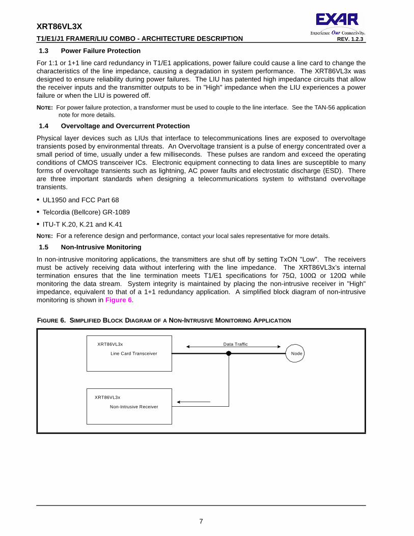
In non-intrusive monitoring applications, the transmitters are shut off by setting TxON "Low". The receiversmust be actively receiving data without interfering with the line impedance. The XRT86VL3x’s internaltermination ensures that the line termination meets T1/E1 specifications for 75Ω, 100Ω or 120Ω whilemonitoring the data stream. System integrity is maintained by placing the non-intrusive receiver in "High"impedance, equivalent to that of a 1+1 redundancy application. A simplified block diagram of non-intrusivemonitoring is shown in Figure 6 .
FIGURE 6. SIMPLIFIED BLOCK DIAGRAM OF A NON-INTRUSIVE MONITORING APPLICATION
Line Card Transceiver
Non-Intrusive Receiver
Node
XRT86VL3x
XRT86VL3x
Data Traffic

XRT86VL3X
8
REV. 1.2.3 T1/E1/J1 FRAMER/LIU COMBO - ARCHITECTURE DESCRIPTIO N
1.6 T1/E1 Serial PCM Interface
The most common mode is the standard serial PCM interface. Within this mode, only the serial data, serialclock, frame pulse and multi-frame pulse are required for both the transmit and receive paths. For the transmitpath, only TxSER is a dedicated input to the device. All other signals to the transmit path in Figure 7 can beprogrammed as either input or output. For the receive path, only RxSER and RxMSYNC are dedicated outputsfrom the device. All other signals in the receive path in Figure 8 can be programmed as either input or output.
FIGURE 7. TRANSMIT T1/E1 SERIAL PCM INTERFACE
FIGURE 8. RECEIVE T1/E1 SERIAL PCM INTERFACE
F TS1TxSER
TxSERclk(bi-directional)
TxSYNC(bi-directional)
TxMSYNC(bi-directional)
TS2 TS24
N : TxMSYNC = 4 * (TxSYNC)SF : TxMSYNC = 12 * (TxSYNC)T1DM : TxMSYNC = 12 * (TxSYNC)SLC-96 : TxMSYNC = 12 * (TxSYNC)ESF : TxMSYNC = 24 * (TxSYNC)
TS1
TxSERclk(bi-directional)
TxSYNC(bi-directional)
TxMSYNC(bi-directional)
TS2 TS32
TxMSYNC = 16 * (TxSYNC)
TxSER
T1
E1
F TS1RxSER
RxSERclk
(bi-directional)
RxSYNC(bi-directional)
RxCRCSYNC
TS2 TS24
N : RxCRCSYNC = 4 * (RxSYNC)SF : RxCRCSYNC = 12 * (RxSYNC)T1DM : RxCRCSYNC = 12 * (RxSYNC)SLC-96 : RxCRCSYNC = 12 * (RxSYNC)ESF : RxCRCSYNC = 24 * (RxSYNC)
TS1
RxSERclk
(bi-directional)
RxSYNC(bi-directional)
RxCASYNC
TS2 TS32
RxCASYNC = 16 * (RxSYNC)
RxSER
T1
E1
XRT86VL3X
9
T1/E1/J1 FRAMER/LIU COMBO - ARCHITECTURE DESCRIPTIO N REV. 1.2.3
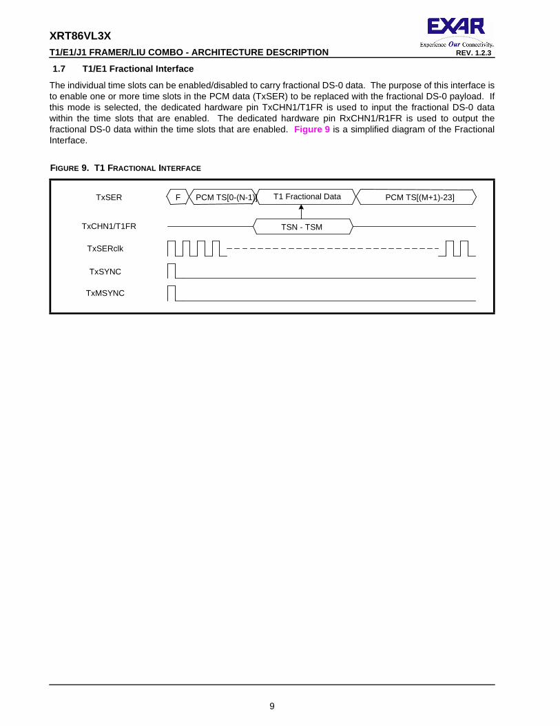
1.7 T1/E1 Fractional Interface
The individual time slots can be enabled/disabled to carry fractional DS-0 data. The purpose of this interface isto enable one or more time slots in the PCM data (TxSER) to be replaced with the fractional DS-0 payload. Ifthis mode is selected, the dedicated hardware pin TxCHN1/T1FR is used to input the fractional DS-0 datawithin the time slots that are enabled. The dedicated hardware pin RxCHN1/R1FR is used to output thefractional DS-0 data within the time slots that are enabled. Figure 9 is a simplified diagram of the FractionalInterface.
FIGURE 9. T1 FRACTIONAL INTERFACE
TSN - TSMTxCHN1/T1FR
TxSERclk
TxSYNC
TxMSYNC
F T1 Fractional DataPCM TS[0-(N-1)] PCM TS[(M+1)-23]TxSER

XRT86VL3X
10
REV. 1.2.3 T1/E1/J1 FRAMER/LIU COMBO - ARCHITECTURE DESCRIPTIO N
1.8 T1/E1 Time Slot Substitution and Control
The time slots within PCM data are reserved for carrying individual DS-0’s. However, the framer block(transmit or receive paths) can substitute the payload with various code definitions. Each time slot can beindependently programmed to carry normal PCM data or a variety of user codes. In E1 mode, the user cansubstitute the transmit time slots 0 and 16, although signaling and Frame Sync cannot be maintained. Thefollowing options for time slot substitution are available:
• Unchanged
• Invert all bits
• Invert even bits
• Invert odd bits
• Programmable User Code
• Busy 0xFF
• Vacant 0xD5
• Busy TS, Busy 00
• A-Law, µ-Law
• Invert the MSB bit
• Invert all bits except the MSB bit
• PRBS
• D/E Channel (or Fractional Input)
FIGURE 10. T1/E1 TIME SLOT SUBSTITUTION AND CONTROL
F
TSn - TSn+m
SubstitutionTxSER
TxSERclk
TxSYNC
TxMSYNC
PCM Data PCM Data
XRT86VL3X
11
T1/E1/J1 FRAMER/LIU COMBO - ARCHITECTURE DESCRIPTIO N REV. 1.2.3
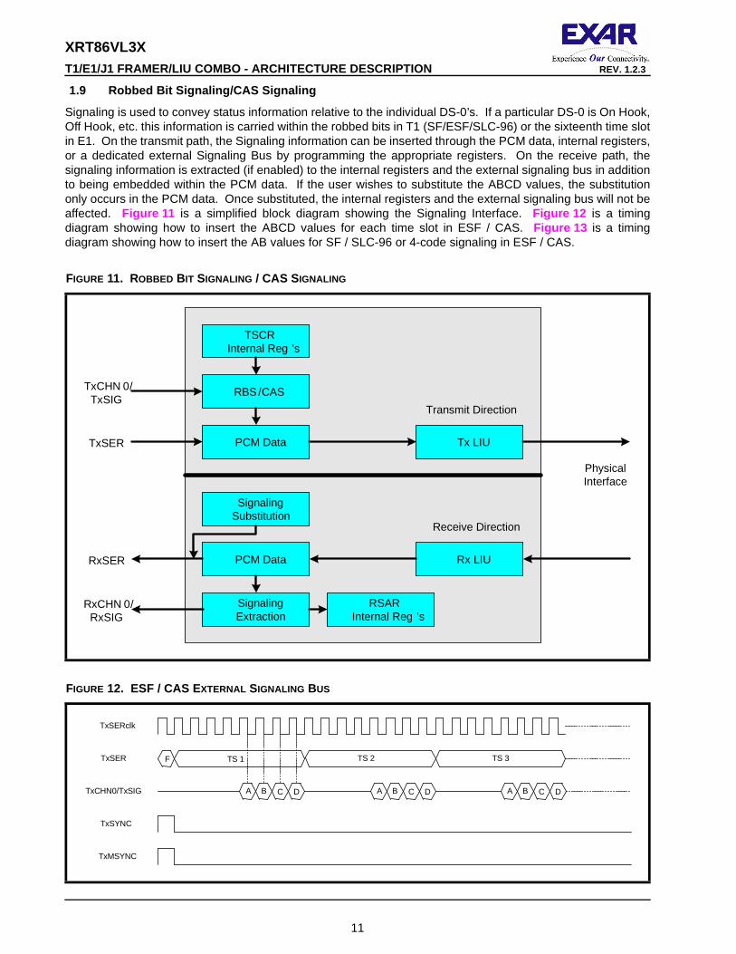
1.9 Robbed Bit Signaling/CAS Signaling
Signaling is used to convey status information relative to the individual DS-0’s. If a particular DS-0 is On Hook,Off Hook, etc. this information is carried within the robbed bits in T1 (SF/ESF/SLC-96) or the sixteenth time slotin E1. On the transmit path, the Signaling information can be inserted through the PCM data, internal registers,or a dedicated external Signaling Bus by programming the appropriate registers. On the receive path, thesignaling information is extracted (if enabled) to the internal registers and the external signaling bus in additionto being embedded within the PCM data. If the user wishes to substitute the ABCD values, the substitutiononly occurs in the PCM data. Once substituted, the internal registers and the external signaling bus will not beaffected. Figure 11 is a simplified block diagram showing the Signaling Interface. Figure 12 is a timingdiagram showing how to insert the ABCD values for each time slot in ESF / CAS. Figure 13 is a timingdiagram showing how to insert the AB values for SF / SLC-96 or 4-code signaling in ESF / CAS.
FIGURE 11. ROBBED BIT SIGNALING / CAS SIGNALING
FIGURE 12. ESF / CAS EXTERNAL SIGNALING BUS
RBS/CAS
SignalingSubstitution
PCM Data Tx LIU
TSCRInternal Reg 's
Rx LIU
SignalingExtraction
PCM Data
RSARInternal Reg 's
Transmit Direction
Receive Direction
TxSER
TxCHN 0/TxSIG
RxSER
RxCHN 0/RxSIG
PhysicalInterface
TxSYNC
TxMSYNC
TxSERclk
TxCHN0/TxSIG
TxSER F
DCBA
TS 1
DCBA DCBA
TS 2 TS 3

XRT86VL3X
12
REV. 1.2.3 T1/E1/J1 FRAMER/LIU COMBO - ARCHITECTURE DESCRIPTIO N
1.10 Overhead Interface
The Overhead interface provides an option for inserting the datalink bits into the transmit PCM data orextracting the datalink bits from the receive PCM data. By default, the datalink information is processed to andfrom the PCM data directly. On the transmit path, the overhead clock is automatically provided as a clockreference to externally time the datalink bits. The user should provide data on the rising edge of the TxOHclkso that the framer can sample the datalink bits on the falling edge. On the receive path, the datalink bits areupdated on the rising edge of the RxOHclk output pin. In T1 ESF mode, a datalink bit occurs every otherframe. Therefore, the default overhead interface is operating at 4kbps. In E1 mode, the datalink bits arelocated in the first time slot of each Non-FAS frame. Figure 14 is a simplified block diagram of the OverheadInterface. Figure 15 is a simplified diagram for the T1 external overhead datalink bus. Figure 16 is asimplified diagram for the E1 external overhead datalink bus.
FIGURE 13. SF / SLC-96 OR 4-CODE SIGNALING IN ESF / CAS EXTERNAL SIGNALING BUS
FIGURE 14. T1/E1 OVERHEAD INTERFACE
TxSYNC
TxMSYNC
TxSERclk
TxCHN0/TxSIG
TxSER F
BA
TS 1
BA BA
TS 2 TS 3
Datalink Bits
PCM Data Tx LIU
Rx LIU
Datalink Bits
PCM Data
Transmit Direction
Receive Direction
TxSER
TxOH
RxSER
RxOH
PhysicalInterface
TxOHclk
RxOHclk

XRT86VL3X
13
T1/E1/J1 FRAMER/LIU COMBO - ARCHITECTURE DESCRIPTIO N REV. 1.2.3
FIGURE 15. T1 EXTERNAL OVERHEAD DATALINK BUS
FIGURE 16. E1 OVERHEAD EXTERNAL DATALINK BUS
TxSYNC
TxOHclk(4kHz)
TxOH
Frame1 Frame6Frame5Frame4Frame2 Frame3
Datalink Bit Datalink Bit Datalink Bit
TxSYNC
TxOHclk
TxOH
Non-FAS Frame FAS Frame
SiTxSER 1 A Sa4 Sa7 Sa8Sa6Sa5
Sa4 Sa7 Sa8If Sa4, Sa7, and Sa8 are Selected

XRT86VL3X
14
REV. 1.2.3 T1/E1/J1 FRAMER/LIU COMBO - ARCHITECTURE DESCRIPTIO N
1.11 Framer Bypass Mode
The framer bypass mode allows the XRT86VL3x to be used as a stand alone Line Interface Unit. In this mode,a few of the backplane interface signals multiplex into the digital Input/output signals to and from the LIU block.Figure 22 shows a simplified block diagram of the framer bypass mode.
FIGURE 17. SIMPLIFIED BLOCK DIAGRAM OF THE FRAMER BYPASS MODE
2-FrameSlip Buffer
Elastic Store
Tx SerialData In
Tx LIUInterface
2-FrameSlip Buffer
Elastic Store
Rx LIUInterface
Rx FramerRx SerialData Out
Tx FramerTCLK=TxSERCLKTPOS=TxSERTNEG=TxSYNC
RCLK=RxSERCLKRPOS=RxSERRNEG=RxSYNC

XRT86VL3X
15
T1/E1/J1 FRAMER/LIU COMBO - ARCHITECTURE DESCRIPTIO N REV. 1.2.3
1.12 High-Speed Non-Multiplexed Interface
The speed of transferring data through a back plane interface in a non-multiplexed manner typically operatesat 1.544Mbps, 2.048Mbps, 4.096Mbps, or 8.192Mbps. For 12.352Mbps and 16.384Mbps, see the High-SpeedMultiplexed Section. The T1/E1 carrier signal out to or in from the line interface is always 1.544MHz and2.048MHz respectively. However, the back plane interface may be synchronous to a “Higher” speed clock.For T1, as shown in Figure 18 , is mapped into an E1 frame. Therefore, every fourth time slot contains non-valid data. For E1, as shown in Figure , is simply synchronized to the “Higher” 8.192MHz clock signal suppliedto the TxMSYNC input pin.
FIGURE 18. T1 HIGH-SPEED NON-MULTIPLEXED INTERFACE
FIGURE 19. E1 HIGH-SPEED NON-MULTIPLEXED INTERFACE
TxSER
TxMSYNC2.048MHz
TxSERCLK(1.544MHz)
TxSYNC
Non-Multiplexed High Speed Interface (2.048MHz/4.096MHz/8.192MHz)
F Don't Care TS 1 TS 2 TS 3 TS 4 TS 5Don't Care
TxSER
TxMSYNC(8.192MHz)
TxSERCLK(2.048MHz)
TxSYNC
Non-Multiplexed High Speed Interface (2.048MHz/4.096MHz/8.192MHz)
TS 1 TS 2 TS 3

XRT86VL3X
16
REV. 1.2.3 T1/E1/J1 FRAMER/LIU COMBO - ARCHITECTURE DESCRIPTIO N
1.13 High-Speed Multiplexed Interface
In addition to the non-multiplexed mode, the framer can interface through the backplane in a high-speedmultiplexed application, either through a bit-muxed or byte-muxed (in HMVIP or H.100) manner. In this mode,the chip is divided into two multiplexed blocks, four channels per block. For T1, the high speed multiplexedmodes are 12.352Mbps (bit-muxed, TxSYNC is “High” during the F-bit), 16.384Mbps (bit-muxed, TxSYNC is“High” during the F-bit), 16.384Mbps (HMVIP: byte-muxed, TxSYNC is “High” during the last 2-bits of theprevious frame and the first 2-bits of the current frame), or 16.384Mbps (H.100: byte-muxed, TxSYNC is “High”during the last bit of the previous frame and the first bit in the current frame). For E1 mode, the only mode thatis not supported is the 12.352Mbps. The only other difference is that the F-bit (for T1 mode) becomes the firstbit of the E1 frame. Figure 20 is a simplified block diagram of transmit bit-muxed application. Figure 21 is asimplified block diagram of receive bit-muxed application. Although the data is only applied to channel 4 orchannel 0, the TxSERCLK is necessary for all channels so that the transmit line rate is always equal to the T1/E1 carrier rate.
FIGURE 20. TRANSMIT HIGH-SPEED BIT MULTIPLEXED BLOCK DIAGRAM
FIGURE 21. RECEIVE HIGH-SPEED B IT MULTIPLEXED BLOCK DIAGRAM
TxSER4
TxMSYNC4(16.384MHz)
TxSERCLK4(2.048MHz)
TxSERCLK5(2.048MHz)
TxSERCLK6(2.048MHz)
TxSERCLK7(2.048MHz)
TTIP/TRing4
TTIP/TRing5
TTIP/TRing6
TTIP/TRing7
4b04b05b0 5b06b0 6b07b07b04b14b15b1 5b16b1 6b17b17b14b24b25b2 5b26b2 6b27b27b2
4b04b14b2
5b05b15b2
6b06b16b2
7b07b17b2
DMUX
TxSYNC4 Bit Interleaved Multiplexed Mode
RxSER4
RxSERCLK4(16.384MHz)
RxLineClk4(2.048MHz)
RxLineClk5(2.048MHz)
RxLineClk6(2.048MHz)
RxLineClk7(2.048MHz)
RTIP/RRing4
RTIP/RRing5
RTIP/RRing6
RTIP/RRing7
4b0 0 05b0 06b0 7b0 0 4b1 0 05b1 06b1 7b1 0 4b2 0 05b2 06b2 7b2 0
4b0 4b1 4b2
5b0 5b1 5b2
6b0 6b1 6b2
7b0 7b1 7b2
MUX
RxSYNC4 Bit Interleaved Multiplexed Mode
RZ Data

XRT86VL3X
17
T1/E1/J1 FRAMER/LIU COMBO - ARCHITECTURE DESCRIPTIO N REV. 1.2.3
2.0 LOOPBACK MODES OF OPERATION
2.1 LIU Physical Interface Loopback Diagnostics
The XRT86VL3x supports several loopback modes for diagnostic testing. The following section describes thelocal analog loopback, remote loopback, digital loopback, and dual loopback modes. The LIU physicalinterface loopback modes are independent from the Framer loopback modes. Therefore, it is possible toconfigure multiple loopback modes creating tremendous flexibility within the looped diagnostic features.
2.1.1 Local Analog Loopback
With local analog loopback activated, the transmit output data at TTIP/TRING is internally looped back to theanalog inputs at RTIP/RRING. External inputs at RTIP/RRING are ignored while valid transmit output datacontinues to be sent to the line. A simplified block diagram of local analog loopback is shown in Figure 22 .
NOTE: The transmit diagnostic features such as TAOS, NLC generation, and QRSS take priority over the transmit inputdata at TCLK/TPOS/TNEG.
2.1.2 Remote Loopback
With remote loopback activated, the receive input data at RTIP/RRING is internally looped back to the transmitoutput data at TTIP/TRING. The remote loopback includes the Receive JA (if enabled). The transmit inputdata at TCLK/TPOS/TNEG are ignored while valid receive output data continues to be sent to the system. Asimplified block diagram of remote loopback is shown in Figure 23 .
FIGURE 22. SIMPLIFIED BLOCK DIAGRAM OF LOCAL ANALOG LOOPBACK
FIGURE 23. SIMPLIFIED BLOCK DIAGRAM OF REMOTE LOOPBACK
Encoder
Decoder
TimingControl
Data andClock
Recovery
JA
JA
Tx
TAOSNLC/PRBS/QRSS
TTIPTRING
RTIPRRING
TCLKTPOSTNEG
RCLKRPOSRNEG
Rx
Encoder
Decoder
TimingControl
Data andClock
Recovery
JA
JA
Tx
Rx
TAOSNLC/PRBS/QRSS
TTIPTRING
RTIPRRING
TCLKTPOSTNEG
RCLKRPOSRNEG
XRT86VL3X
18
REV. 1.2.3 T1/E1/J1 FRAMER/LIU COMBO - ARCHITECTURE DESCRIPTIO N
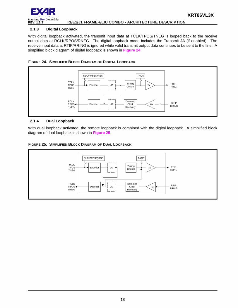
2.1.3 Digital Loopback
With digital loopback activated, the transmit input data at TCLK/TPOS/TNEG is looped back to the receiveoutput data at RCLK/RPOS/RNEG. The digital loopback mode includes the Transmit JA (if enabled). Thereceive input data at RTIP/RRING is ignored while valid transmit output data continues to be sent to the line. Asimplified block diagram of digital loopback is shown in Figure 24 .
2.1.4 Dual Loopback
With dual loopback activated, the remote loopback is combined with the digital loopback. A simplified blockdiagram of dual loopback is shown in Figure 25 .
FIGURE 24. SIMPLIFIED BLOCK DIAGRAM OF DIGITAL LOOPBACK
FIGURE 25. SIMPLIFIED BLOCK DIAGRAM OF DUAL LOOPBACK
Encoder
Decoder
TimingControl
Data andClock
Recovery
JA
JA
Tx
Rx
TAOSNLC/PRBS/QRSS
TTIPTRING
RTIPRRING
TCLKTPOSTNEG
RCLKRPOSRNEG
Encoder
Decoder
TimingControl
Data andClock
Recovery
JA
JA
Tx
Rx
TAOSNLC/PRBS/QRSS
TTIPTRING
RTIPRRING
TCLKTPOSTNEG
RCLKRPOSRNEG
XRT86VL3X
19
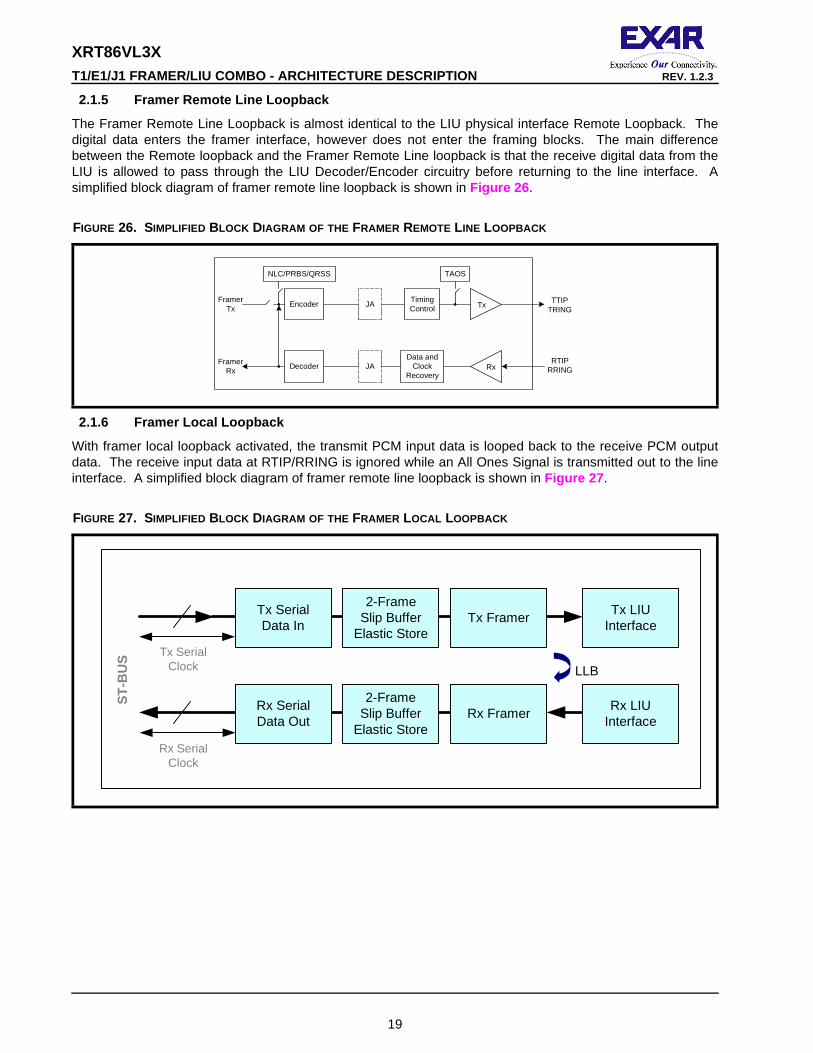
T1/E1/J1 FRAMER/LIU COMBO - ARCHITECTURE DESCRIPTIO N REV. 1.2.3
2.1.5 Framer Remote Line Loopback
The Framer Remote Line Loopback is almost identical to the LIU physical interface Remote Loopback. Thedigital data enters the framer interface, however does not enter the framing blocks. The main differencebetween the Remote loopback and the Framer Remote Line loopback is that the receive digital data from theLIU is allowed to pass through the LIU Decoder/Encoder circuitry before returning to the line interface. Asimplified block diagram of framer remote line loopback is shown in Figure 26 .
2.1.6 Framer Local Loopback
With framer local loopback activated, the transmit PCM input data is looped back to the receive PCM outputdata. The receive input data at RTIP/RRING is ignored while an All Ones Signal is transmitted out to the lineinterface. A simplified block diagram of framer remote line loopback is shown in Figure 27 .
FIGURE 26. SIMPLIFIED BLOCK DIAGRAM OF THE FRAMER REMOTE LINE LOOPBACK
FIGURE 27. SIMPLIFIED BLOCK DIAGRAM OF THE FRAMER LOCAL LOOPBACK
Encoder
Decoder
TimingControl
Data andClock
Recovery
JA
JA
Tx
Rx
TAOSNLC/PRBS/QRSS
TTIPTRING
RTIPRRING
FramerTx
FramerRx
Tx SerialClock
Rx SerialClock
ST
-BU
S
2-FrameSlip Buffer
Elastic Store
Tx SerialData In
Tx LIUInterface
2-FrameSlip Buffer
Elastic Store
Rx LIUInterface
Rx FramerRx SerialData Out
Tx Framer
LLB

XRT86VL3X
20
REV. 1.2.3 T1/E1/J1 FRAMER/LIU COMBO - ARCHITECTURE DESCRIPTIO N
3.0 HDLC CONTROLLERS AND LAPD MESSAGES
The purpose of the HDLC controllers is to allow messages to be stored for transport in the outbound transmitframer block or extracted from the receive framer block through the LAPD interface. Each channel within theFramer has 3 independent HDLC controllers. Each HDLC controller has two 96-Byte buffers for Transmit andtwo 96-Byte buffers for Receive. The buffers are used to insert messages into the out going data stream forTransmit or to extract messages from the incoming data stream from the Receive path. Total, there are twelve96-Byte buffers per channel. This allows multiple HDLC messages to be transported to and from EXAR’sframing device.
FIGURE 28. HDLC CONTROLLERS
Buffer 0 Buffer 1
Transmit
Receive
96-Bytes 96-Bytes
96-Bytes 96-Bytes
Transmit
Receive
96-Bytes 96-Bytes
96-Bytes 96-Bytes
Transmit
Receive
96-Bytes 96-Bytes
96-Bytes 96-Bytes
HDLC1
HDLC2
HDLC3
Buffer 0 Buffer 1
Buffer 0 Buffer 1
Channel N

XRT86VL3X
21
T1/E1/J1 FRAMER/LIU COMBO - ARCHITECTURE DESCRIPTIO N REV. 1.2.3
3.1 Storing and Retrieving Message Contents
Each buffer has its own dedicated internal holding register. To access the contents of these buffers or to storemessages, the XRT86VL3x utilizes a multiplexed access. The buffers are broken down into Buffer 0 or Buffer1. Register 0xn600 is used to Read or Write to Buffer 0 of the selected HDLC controller, while register 0xn700is used to Read or Write to Buffer 1 of the selected HDLC controller. Although, each HDLC controller has itsown dedicated register set for control, the message contents of only one controller can be accessed at onetime through the microprocessor or DMA interface.
FIGURE 29. STORING AND RETRIEVING MESSAGE CONTENTS
96-Bytes
HDLC1 Buffer 0
96-Bytes
HDLC2 Buffer 0
96-Bytes
HDLC3 Buffer 0
96-Bytes
HDLC1 Buffer 1
96-Bytes
HDLC2 Buffer 1
96-Bytes
HDLC3 Buffer 1
Register 0xn700MUX
Register 0xn600MUX

XRT86VL3X
22
REV. 1.2.3 T1/E1/J1 FRAMER/LIU COMBO - ARCHITECTURE DESCRIPTIO N
3.2 Programming Sequence for Sending HDLC Messages
Once the data link source and the type of message has been chosen, the following programming sequencecan be followed to send any length message.
FIGURE 30. SENDING HDLC MESSAGES
Enable TxSOT and TxEOT
Read TxBYTE Count Register
Write Number of Bytes to the TxBYTE Count Register
If < or = to96-Bytes
Enable HDLC and TxIDLE Code
TxEOT Indicates End of Message Transmission
Enable HDLC Only(No IDLE Code)
Wait for TxSOT
YES
NO
Store Message in Available TxBuffer

XRT86VL3X
23
T1/E1/J1 FRAMER/LIU COMBO - ARCHITECTURE DESCRIPTIO N REV. 1.2.3
3.3 Programming Sequence for Receiving LAPD Messages
The XRT86VL3x can extract data link information from incoming DS1 frames from either the datalink bitsthemselves or the D/E time slots within the PCM input data. To extract a LAPD message, the followingprogramming sequence can be used as a reference.
FIGURE 31. RECEIVING HDLC MESSAGES
Enable RxSOT, RxEOT, and RxIDLE
RxSOT Indicates a Start of a New Message, go to Next
Step
Wait for RxEOT or RxIDLE
If INT = RxIDLERead RxBYTE Count Register to Determine
Available Buffer
Read the Buffer to Retrieve the Message
Read RxBYTE Count Register to Determine
Available Buffer
Read the Buffer to Retrieve the Message
YES, RxIDLE
NO, RxEOT
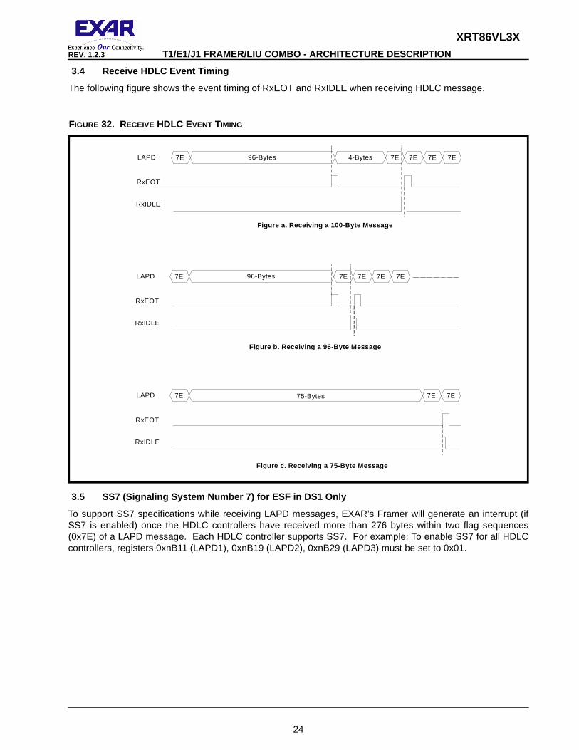
XRT86VL3X
24
REV. 1.2.3 T1/E1/J1 FRAMER/LIU COMBO - ARCHITECTURE DESCRIPTIO N
3.4 Receive HDLC Event Timing
The following figure shows the event timing of RxEOT and RxIDLE when receiving HDLC message.
3.5 SS7 (Signaling System Number 7) for ESF in DS1 O nly
To support SS7 specifications while receiving LAPD messages, EXAR’s Framer will generate an interrupt (ifSS7 is enabled) once the HDLC controllers have received more than 276 bytes within two flag sequences(0x7E) of a LAPD message. Each HDLC controller supports SS7. For example: To enable SS7 for all HDLCcontrollers, registers 0xnB11 (LAPD1), 0xnB19 (LAPD2), 0xnB29 (LAPD3) must be set to 0x01.
FIGURE 32. RECEIVE HDLC EVENT TIMING
96-Bytes 4-Bytes 7E 7E 7E 7E7ELAPD
RxEOT
RxIDLE
96-Bytes 7E 7E 7E 7E7ELAPD
RxEOT
RxIDLE
75-Bytes 7E 7E7ELAPD
RxEOT
RxIDLE
Figure a. Receiving a 100-Byte Message
Figure c. Receiving a 75-Byte Message
Figure b. Receiving a 96-Byte Message

XRT86VL3X
25
T1/E1/J1 FRAMER/LIU COMBO - ARCHITECTURE DESCRIPTIO N REV. 1.2.3
3.6 DS1/E1 Datalink Transmission Using the HDLC Cont rollers
The transmit framer block can insert data link information to outbound DS1/E1 frames. The data linkinformation can be inserted from the following sources.
• Transmit Overhead Input Interface (TxOH)
• Transmit HDLC1 Controller
• Transmit Serial Input Interface (TxSER)
NOTE: HDLC1 is the dedicated controller for transmission of LAPD messages through the datalink bits. If the datalink bitsare not used for LAPD messages, then HDLC1 can be used through the D/E time slots as with HDLC2 and HDLC3.
The Transmit Data Link Source Select bits within the Transmit Data Link Select Register (TSDLSR) determinethe source for the data link bits in ESF, SLC®96, or T1DM for DS1 and CRC multi frame for E1. Each TransmitHDLC Controller contains four major functional modules.
• Bit-Oriented Signaling Processor
• LAPD Controller
• SLC®96 Data Link Controller
• Automatic Performance Report (APR) Generation
3.7 Transmit BOS (Bit Oriented Signaling) Processor
The Transmit BOS Processor handles transmission of BOS messages through the data link channel. Theprocessor can be set for a specific amount of repetitions a certain BOS message will be transmitted, or it maybe placed in an infinite loop. The processor can also insert a BOS IDLE flag sequence and/or an ABORTsequence to be transmitted on the data link channel.
3.7.1 Description of BOS
Bit-Oriented Signaling messages are a 16-bit pattern of which a 6-bit message is embedded as shown in thefollowing table.
Where D5 is the MSB and D0 is the LSB. The rightmost "1" is transmitted first. BOS is classified into thefollowing two groups.
• Priority Codeword Message
• Command and Response Information
3.7.2 Priority Codeword Message
A Priority Codeword Message is preemptive and has the highest priority among all data link information. APriority Codeword indicates a condition that is affecting the quality of service and thus shall be transmitted untilthe condition no longer exists. The duration of transmission should not be less than one second. A prioritycodeword may be interrupted by software for 100 milliseconds to send maintenance commands with aminimum interval of one second between interruptions. Yellow alarm (00000000 11111111) is the only prioritymessage defined in industry standards.
3.7.3 Command and Response Information
Command and Response Information is transmitted to perform various functions. The BOS Processor cansend a command and response by transmitting a minimum of 10 repetitions of the appropriate codewordpattern. A Command and response data transmission initiates action at the remote end, while the remote endwill respond by sending Bit-Oriented response message to acknowledge the received commands. Theactivation and deactivation of line remote loop-back and local payload loop-back functions are of this type.
BOS MESSAGE FORMAT
0 D5 D4 D3 D2 D1 D0 0 1 1 1 1 1 1 1 1
XRT86VL3X
26
REV. 1.2.3 T1/E1/J1 FRAMER/LIU COMBO - ARCHITECTURE DESCRIPTIO N
3.8 Transmit MOS (Message Oriented Signaling) Proces sor
The Transmit LAPD controller implements the Message-Oriented protocol based on ITU RecommendationQ.921 Link Access Procedures on the D-channel. It provides the following functions.
• Zero stuffing
• T1/E1 transmitter interface
• Transmit message buffer access
• Frame check sequence generation
• IDLE flag insertion
• ABORT sequence generation
Two 96-byte buffers in shared memory are allocated for each LAPD to reduce the frequency of microprocessorinterrupts and alleviate the response time requirement for a microprocessor to handle each interrupt. Thereare no restrictions on the length of the message. However the 96-byte buffer is deep enough to hold one entireLAPD path or test signal identification message.
3.8.1 Discussion of MOS
Message-Oriented signals sent by the transmit LAPD Controller are messages conforming to ITURecommendation Q.921 LAPD protocol. There are two types of Message-Oriented signals. One is a periodicperformance report generated by the source or sink T1/E1 terminals as defined by ANSI T1.403. The other isa path or test signal identification message that may be optionally generated by a terminal or intermediateequipment on a T1/E1 circuit. The message structures of the performance report and path or test signalidentification message are shown in Figure 33 for format A and format B respectively.

XRT86VL3X
27
T1/E1/J1 FRAMER/LIU COMBO - ARCHITECTURE DESCRIPTIO N REV. 1.2.3
3.8.2 Periodic Performance Report
The ANSI T1.403 standard requires that the status of the transmission quality be reported in one-secondintervals. The one-second timing may be derived from the DS1 signal or from a separate equally accurate(±32ppm) source. The phase of the one-second periods does not depend on the time of occurrence of anyerror event. A total of four seconds of information is transmitted so that recovery operations may be initiated incase an error corrupts a message. Counts of events shall be accumulated in each contiguous one-secondinterval. At the end of each one-second interval, a modulo-4 counter shall be incremented, and the appropriateperformance bits shall be set in bytes 5 and 6 in Format A. These octets and the octets that carry theperformance bits of the preceding three one-second intervals form the periodic performance report.
The periodic performance report is made up of 14 bytes of data. Bytes 1 to 4, 13, and 14 are the messageheader and bytes 5 to 12 contain data regarding the four most-recent one-second intervals. The periodicperformance report message uses the SAPI/TEI value of 0x14.
3.8.3 Transmission-Error Event
Occurrences of transmission-error events indicate the quality of transmission. The occurrences that shall bedetected and reported are:
• CRC Error Event: A CRC-6 error event is the occurrence of a received CRC code that is not identical to thecorresponding locally calculated code.
• Severely Errored Framing Event: A severely-errored-framing event is the occurrence of two or more framing-bit-pattern errors within a 3-ms period. Contiguous 3-ms intervals shall be examined. The 3-ms period maycoincide with the ESF. The severely-errored-framing event, while similar in form to criteria for declaring a
FIGURE 33. LAPD FRAME STRUCTURE
XRT86VL3X
28
REV. 1.2.3 T1/E1/J1 FRAMER/LIU COMBO - ARCHITECTURE DESCRIPTIO N
terminal has lost framing, is only designed as a performance indicator; existing terminal out-of-frame criteriawill continue to serve as the basis for terminal alarms.
• Frame-Synchronization-Bit Error Event: A frame-synchronization-bit-error event is the occurrence of areceived framing-bit-pattern not meeting the severely-errored-framing event criteria.
• Line-Code Violation event: A line-code violation event is a bipolar violation of the incoming data. A line-codeviolation event for an B8ZS-coded signal is the occurrence of a received excessive zeros (EXZ) or a bipolarviolation that is not part of a zero-substitution code.
• Controlled Slip Event: A controlled-slip event is a replication, or deletion, of a T1 frame by the receivingterminal. A controlled slip may occur when there is a difference between the timing of a synchronousreceiving terminal and the received signal.
3.8.4 Path and Test Signal Identification Message
The path identification message is used to identify the path between the source terminal and the sink terminal.The test signal identification message is used by test signal generating equipment. Both identificationmessages are made up of 82 bytes of data. Byte 1 to 4, 81 and 82 are the message header and bytes 5 to 80contain six data elements. These messages use the SAPI/TEI value of 0x15 to differentiate themselves fromthe performance report message.
3.8.5 Frame Structure
The message structure of message-oriented signal is shown in Figure 33 . Two format types are shown in thefigure: format A for frames which are sending performance report message and format B for frames whichcontaining a path or test signal identification message. The following abbreviations are used:
• SAPI: Service Access Point Identifier
• C/R: Command or Response
• EA: Extended Address
• TEI: Terminal Endpoint Identifier
• FCS: Frame Check Sequence
3.8.6 Flag Sequence
All frames shall start and end with the flag sequence consisting of one 0 bit followed by six contiguous 1 bitsand one 0 bit. The flag preceding the address field is defined as the opening flag. The flag following the FrameCheck Sequence (FCS) field is defined as the closing flag. The closing flag may also serve as the opening flagof the next frame, in some applications. However, all receivers must be able to accommodate receipt of one ormore consecutive flags.
3.8.7 Address Field
The address field consists of two octets. A single octet address field is reserved for LAPB operation in order toallow a single LAPB data link connection to be multiplexed along with LAPD data link connections.
3.8.8 Address Field Extension bit (EA)
The address field range is extended by reserving bit 1 of the address field octets to indicate the final octet ofthe address field. The presence of a 1 in bit 1 of an address field octet signals that it is the final octet of theaddress field. The double octet address field for LAPD operation shall have bit 1 of the first octet set to a 0 andbit 1 of the second octet set to 1.
3.8.9 Command or Response bit (C/R)
The Command or Response bit identifies a frame as either a command or a response. The user side shallsend commands with the C/R bit set to 0, and responses with the C/R bit set to 1. The network side shall do theopposite; That is, commands are sent with C/R bit set to 1, and responses are sent with C/R bit set to 0.

XRT86VL3X
29
T1/E1/J1 FRAMER/LIU COMBO - ARCHITECTURE DESCRIPTIO N REV. 1.2.3
3.8.10 Service Access Point Identifier (SAPI)
The Service Access Point Identifier identifies a point at which data link layer services are preceded by a datalink layer entity type to a layer 3 or management entity. Consequently, the SAPI specifies a data link layer entitytype that should process a data link layer frame and also a layer 3 or management entity, which is to receiveinformation carried by the data link layer frame. The SAPI allows 64 service access points to be specified,where bit 3 of the address field octet containing the SAPI is the least significant binary digit and bit 8 is the mostsignificant. SAPI values are 0x14 and 0x15 for performance report message and path or test signalidentification message respectively.
3.8.11 Terminal Endpoint Identifier (TEI)
The TEI sub-field allows 128 values where bit 2 of the address field octet containing the TEI is the leastsignificant binary digit and bit 8 is the most significant binary digit. The TEI sub-field bit pattern 111 1111 (=127)is defined as the group TEI. The group TEI is assigned permanently to the broadcast data link connectionassociated with the addressed Service Access Point (SAP). TEI values other than 127 are used for the point-to-point data link connections associated with the addressed SAP. Non-automatic TEI values (0-63) areselected by the user, and their allocation is the responsibility of the user. The network automatically selectsand allocates TEI values (64-126).
3.8.12 Control Field
The control field identifies the type of frame which will be either a command or response. The control field shallconsist of one or two octets. Three types of control field formats are specified: 2-octet numbered informationtransfer (I format), 2-octet supervisory functions (S format), and single-octet unnumbered information transfersand control functions (U format). The control field for T1/E1 message is categorized as a single-octetunacknowledged information transfer having the value 0x03.
3.8.13 Frame Check Sequence (FCS) Field
The source of either the performance report or an identification message shall generate the frame checksequence. The FCS field shall be a 16-bit sequence. It shall be the ones complement of the sum (modulo 2)of:
• The remainder of xk (x15 + x14 + x13 + x12 + x11 + x10 + x9 + x8 + x7 + x6 + x5 + x4 + x3 + x2 + x + 1)divided (modulo 2) by the generator polynomial x16 + x12 + x5 + 1, where k is the number of bits in the frameexisting between, but not including, the final bit of the opening flag and the first bit of the FCS, excluding bitsinserted for transparency, and
• The remainder of the division (modulo 2) by the generator polynomial x16 + x12 + x5 + 1, of the product ofx16 by the content of the frame existing between, but not including, the final bit of the opening flag and thefirst bit of the FCS, excluding bits inserted for transparency.
As a typical implementation at the transmitter, the initial content of the register of the device computing theremainder of the division is preset to all 1s and is then modified by division by the generator polynomial on theaddress, control and information fields; the ones complement of the resulting remainder is transmitted as the16-bit FCS.
As a typical implementation at the receiver, the initial content of the register of the device computing theremainder is preset to all 1s. The final remainder, after multiplication by x16 and then division (modulo 2) by thegenerator polynomial x16 + x12 + x5 + 1 of the serial incoming protected bits and the FCS, will be0001110100001111 (x15 through x0, respectively) in the absence of transmission errors.
3.8.14 Transparency (Zero Stuffing)
A transmitting data link layer entity shall examine the frame content between the opening and closing flagsequences, (address, control, information and FCS field) and shall insert a 0 bit after all sequences of fivecontiguous 1 bits (including the last five bits of the FCS) to ensure that an IDLE flag or an Abort sequence isnot simulated within the frame. A receiving data link layer entity shall examine the frame contents between theopening and closing flag sequences and shall discard any 0 bit which directly follows five contiguous 1 bits.

XRT86VL3X
30
REV. 1.2.3 T1/E1/J1 FRAMER/LIU COMBO - ARCHITECTURE DESCRIPTIO N
3.9 Transmit SLC®96 Data link Controller
The SLC®96 T1 format is invented by AT&T and is used between the Digital Switch and a SLC®96 formattedremote terminal. The purpose of the SLC®96 product is to provide standard telephone service or Plain OldTelephone Service (POTS) in areas of high subscriber density but back-haul the traffic over T1 facilities.
To support the SLC®96 formatted remote terminal equipment, which is likely in an underground location, theT1 framer must:
• Indicate equipment failures of the equipment to maintenance personal
• Indicate failures of the POTS lines
• Test the POTS lines
• Provide redundancy on the T1s
The SLC®96 framing format is a D4 Super-frame (SF) format with specialized data link information bits. Thesedata link information bits take the position of the Super-frame Alignment (Fs) bit positions. These bits consist ofthe following.
• Concentrator bits (C, bit position 1 to 11)
• First Spoiler bits (FS, bit position 12 to 14)
• Maintenance bits (M, bit position 15 to 17)
• Alarm bits (A, bit position 18 to 19)
• Protection Line Switch bits (S, bit position 20 to 23)
• Second Spoiler bit (SS, bit position 24)
• Resynchronization pattern (000111000111)
In SLC®96 mode, a six 6-bit datalink message will generate a one 9-ms frame of the SLC®96 messageformat. The format of the datalink message is given in BELLCORE TR-TSY-000008. When SLC®96 mode isenabled, the Fs bit is replaced by the data link message read from memory at the beginning of each D4 super-frame. The XRT86VL3x allocates two 6-byte buffers to provide the SLC®96 Data Link Controller an alternatingaccess mechanism for information transmission. The bit ordering and usage is shown in the following table;and the LSB is sent first. Note that these registers are memory-based storage and they need to be initialized.
Each register is read out of memory once every six SF super-frames. The memory holding these registersowns a shared memory structure that is used by multiple devices. These include DS1 transmit module, DS1receive module, Transmit LAPD Controller, Transmit SLC®96 Data Link controller, Bit-Oriented SignalingProcessor, Receive LAPD Controller, Receive SLC®96 Data Link Controller, Receive Bit-Oriented SignalingProcessor and microprocessor interface module.
TABLE 1: B IT ORDERING AND USAGE
BYTE 5 4 3 2 1 0
1 0 1 1 1 0 0
2 C1 1 1 1 0 0
3 C7 C6 C5 C4 C3 C2
4 1 0 C11 C10 C9 C8
5 A2 A1 M3 M2 M1 0
6 0 1 S4 S3 S2 S1

XRT86VL3X
31
T1/E1/J1 FRAMER/LIU COMBO - ARCHITECTURE DESCRIPTIO N REV. 1.2.3
3.10 D/E Time Slot Transmit HDLC Controller Block V5 .1 or V5.2 Interface
V5.2 protocol specifies a provision for transmitting simultaneous LAPD messages. Since only one messagecan be sent through the datalink bits at one time, an alternative path for communication is offered within theframer block. This alternative path is known as D or E channel which can be transmitted through one or moreof the DS-0 time slots. D channel is used primarily for data link applications. E channel is used primarily forsignaling for circuit switching with multiple access configurations. A range of time slots can be dedicated toHDLC1, while a different range of time slots can be dedicated to HDLC2 to support V5.2. In addition, HDLC3can be used to transmit a third LAPD message if desired. The HDLC controllers are implemented in the samemanner as the datalink described above with the exception of the data link source select bits.
3.11 Automatic Performance Report (APR)
The APR feature allows the system to transmit PMON status within a LAPD Framing format A at one secondintervals or within a single shot report. The data octets 5 through 12 within the LAPD frame are replaced withthe PMON status for the previous one second interval.
NOTE: The right most bit (bit 1) is transmitted first for all fields except for the two bytes of the FCS that are transmitted leftmost bit (bit 8) first.
3.11.1 Bit Value Interpretation
G1 = 1 if number of CRC error events is equal to 1
G2 = 1 if number of CRC error events is greater than 1 or equal to 5
G3 = 1 if number of CRC error events is greater than 5 or equal to 10
G4 = 1 if number of CRC error events is greater than 10 or equal to 100
G5 = 1 if number of CRC error events is greater than 100 or equal to 319
G6 = 1 if number of CRC error events is equal to 320
SE = 1 if a severely errored framing event occurs (FE shall be 0)
FE = 1 if a framing synchronization bit error event occurs (SE shall be 0)
LV = 1 if a line code violation event occurs
SL = 1 if slip event within the slip buffer occurs
TABLE 2: FRAMING FORMAT FOR PMON STATUS INSERTED WITHIN LAPD BY INITIATING APR
Octet Number 8 7 6 5 4 3 2 1 Time (s)12 CR EA=03 EA=14
5 G3 LV G4 U1 U2 G5 SL G6 T0
6 FE SE LB G1 R G2 Nm Ni
7 G3 LV G4 U1 U2 G5 SL G6 T0 - 1
8 FE SE LB G1 R G2 Nm Ni
9 G3 LV G4 U1 U2 G5 SL G6 T0 - 2
10 FE SE LB G1 R G2 Nm Ni
11 G3 LV G4 U1 U2 G5 SL G6 T0 - 3
12 FE SE LB G1 R G2 Nm Ni131415
Flag = 01111110SAPI = 001110TEI = 0000000
Control = 00000011 = Unacknowledged Frame
FCS
Flag = 01111110FCS

XRT86VL3X
32
REV. 1.2.3 T1/E1/J1 FRAMER/LIU COMBO - ARCHITECTURE DESCRIPTIO N
LB = 1 if payload loopback is activated
U1 = If SPRM is used, this bit is controlled by register 0xN142 (default = 0)
U2 = If SPRM is used, this bit is controlled by register 0xN142 (default = 0)
R = If SPRM is used, these bits are controlled by register 0xN142 (default = 0000)
NmNi = One second report module 4 count

XRT86VL3X
33
T1/E1/J1 FRAMER/LIU COMBO - ARCHITECTURE DESCRIPTIO N REV. 1.2.3
4.0 OVERHEAD INTERFACE BLOCK
The XRT86VL3x has the ability to extract or insert DS1 data link information from or into the following:
• Facility Data Link (FDL) bits in ESF framing format mode
• Signaling Framing (Fs) bits in SLC®96 and N framing format mode
• Remote Signaling (R) bits in T1DM framing format mode
The source and destination of these inserted and extracted data link bits would be from either the internalHDLC Controller or the external device accessible through DS1 Overhead Interface Block. The operation ofthe Transmit Overhead Input Interface Block and the Receive Overhead Output Interface Block will bediscussed separately.
4.1 DS1 Transmit Overhead Input Interface Block
4.1.1 Description of the DS1 Transmit Overhead Input Interface Block
The DS1 Transmit Overhead Input Interface Block will allow an external device to be the provider of the FacilityData Link (FDL) bits in ESF framing format mode, Signaling Framing (Fs) bits in the SLC96 and N framingformat mode and Remote Signaling (R) bit in T1DM framing format mode. This interface provides interfacesignals and required interface timing to shift in proper data link information at proper time.
The Transmit Overhead Input Interface for a given Framer consists of two signals.
• TxOHClk_n: The Transmit Overhead Input Interface Clock Output signal
• TxOH_n: The Transmit Overhead Input Interface Input signal.
The Transmit Overhead Input Interface Clock Output pin (TxOHCLK_n) generates a rising clock edge for eachdata link bit position according to configuration of the framer. The Data Link equipment interfaced to theTransmit Overhead Input Interface block should update the data link bits on the TxOH_n line upon detection ofthe rising edge of TxOHClk_n. The Transmit Overhead Input Interface block will sample and latch the data linkbits on the TxOH_n line on the falling edge of TxOHClk_n. The data link bits will be included and transmittedvia the outgoing DS1 frames.
The figure below shows block diagram of the DS1 Transmit Overhead Input Interface of XRT86VL3x.
4.1.2 Configure the DS1 Transmit Overhead Input Inte rface module as source of the Facility DataLink (FDL) bits in ESF framing format mode
The FDL bits in ESF framing format mode can be inserted from:
• DS1 Transmit Overhead Input Interface Block
• DS1 Transmit HDLC Controller
• DS1 Transmit Serial Input Interface.
FIGURE 34. BLOCK DIAGRAM OF THE DS1 TRANSMIT OVERHEAD INPUT INTERFACE OF THE XRT86VL3X
TransmitOverhead Input
Interface
TxOH_n
TxOHClk_n
To TransmitFramer Block

XRT86VL3X
34
REV. 1.2.3 T1/E1/J1 FRAMER/LIU COMBO - ARCHITECTURE DESCRIPTIO N
The Transmit Data Link Source Select bits of the Transmit Data Link Select Register (TDLSR) controls theinsertion of data link bits into the FDL bits in ESF framing format mode. The table below shows configuration ofthe Transmit Data Link Source Select bits of the Transmit Data Link Select Register (TDLSR).
If the Transmit Data Link Source Select bits of the Transmit Data Link Select Register are set to 10, theTransmit Overhead Input Interface Block becomes input source of the FDL bits.
The XRT86VL3x allows the user to select bandwidth of the Facility Data Link Channel in ESF framing formatmode. The FDL can be either a 4KHz or 2KHz data link channel. The Transmit Data Link Bandwidth Select bitsof the Transmit Data Link Select Register (TDLSR) determine the bandwidth of FDL channel in ESF framingformat mode.
The table below shows configuration of the Transmit Data Link Bandwidth Select bits of the Transmit Data LinkSelect Register (TDLSR).)
Figure 35 below shows the timing diagram of the input and output signals associated with the DS1 TransmitOverhead Input Interface module in ESF framing format mode.
TRANSMIT DATA LINK SELECT REGISTER (TDLSR) (ADDRESS = 0XN10AH)
BIT NUMBER
BIT NAME BIT TYPE BIT DESCRIPTION
1-0 Transmit Data Link Source Select
R/W 00 - The Facility Data Link bits are inserted into the framer through either the LAPD controller or the SLC®96 buffer.
01 - The Facility Data Link bits are inserted into the framer through the Transmit Serial Data input Interface via the TxSer_n pins.
10 - The Facility Data Link bits are inserted into the framer through the Transmit Overhead Input Interface via the TxOH_n pins.
11 - The Facility Data Link bits are forced to one by the framer.
TRANSMIT DATA LINK SELECT REGISTER (TDLSR) (ADDRESS = 0XN10AH)
BIT NUMBER
BIT NAME BIT TYPE BIT DESCRIPTION
5-4 Transmit Data Link Bandwidth Select
R/W 00 - The Facility Data Link is a 4KHz channel. All available FDL bits (first bit of every other frame) are used as data link bits.
01 - The Facility Data Link is a 2KHz channel. Only the odd FDL bits (first bit of frame 1, 5, 9…) are used as data link bits.
10 - The Facility Data Link is a 2KHz channel. Only the even FDL bits (first bit of frame 3, 7, 11…) are used as data link bits.

XRT86VL3X
35
T1/E1/J1 FRAMER/LIU COMBO - ARCHITECTURE DESCRIPTIO N REV. 1.2.3
4.1.3 Configure the DS1 Transmit Overhead Input Inte rface module as source of the SignalingFraming (Fs) bits in N or SLC®96 framing format mod e
The Fs bits in SLC®96 and N framing format mode can be inserted from:
• DS1 Transmit Overhead Input Interface Block
• DS1 Transmit HDLC Controller
• DS1 Transmit Serial Input Interface.
The Transmit Data Link Source Select bits of the Transmit Data Link Select Register (TDLSR) controls theinsertion of data link bits into the Fs bits in N or SLC®96 framing format mode. The table below showsconfiguration of the Transmit Data Link Source Select bits of the Transmit Data Link Select Register (TDLSR).
If the Transmit Data Link Source Select bits of the Transmit Data Link Select Register are set to 10, theTransmit Overhead Input Interface Block becomes input source of the Fs bits.
FIGURE 35. DS1 TRANSMIT OVERHEAD INPUT INTERFACE TIMING IN ESF FRAMING FORMAT MODE
TRANSMIT DATA LINK SELECT REGISTER (TDLSR) (ADDRESS = 0XN10AH)
BIT NUMBER
BIT NAME BIT TYPE BIT DESCRIPTION
1-0 Transmit Data Link Source Select
R/W 00 - The Signaling Framing bits are inserted into the framer through either the LAPD controller or the SLC®96 buffer.
01 - The Signaling Framing bits are inserted into the framer through the Transmit Serial Data input Interface via the TxSer_n pins.
10 - The Signaling Framing bits are inserted into the framer through the Transmit Overhead Input Interface via the TxOH_n pins.
11 - The Signaling Framing bits are forced to one by the framer.
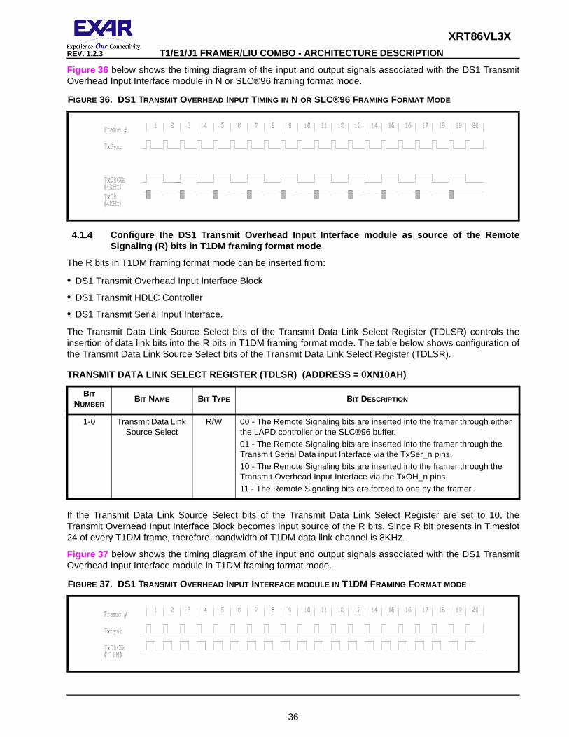
XRT86VL3X
36
REV. 1.2.3 T1/E1/J1 FRAMER/LIU COMBO - ARCHITECTURE DESCRIPTIO N
Figure 36 below shows the timing diagram of the input and output signals associated with the DS1 TransmitOverhead Input Interface module in N or SLC®96 framing format mode.
4.1.4 Configure the DS1 Transmit Overhead Input Inte rface module as source of the RemoteSignaling (R) bits in T1DM framing format mode
The R bits in T1DM framing format mode can be inserted from:
• DS1 Transmit Overhead Input Interface Block
• DS1 Transmit HDLC Controller
• DS1 Transmit Serial Input Interface.
The Transmit Data Link Source Select bits of the Transmit Data Link Select Register (TDLSR) controls theinsertion of data link bits into the R bits in T1DM framing format mode. The table below shows configuration ofthe Transmit Data Link Source Select bits of the Transmit Data Link Select Register (TDLSR).
If the Transmit Data Link Source Select bits of the Transmit Data Link Select Register are set to 10, theTransmit Overhead Input Interface Block becomes input source of the R bits. Since R bit presents in Timeslot24 of every T1DM frame, therefore, bandwidth of T1DM data link channel is 8KHz.
Figure 37 below shows the timing diagram of the input and output signals associated with the DS1 TransmitOverhead Input Interface module in T1DM framing format mode.
FIGURE 36. DS1 TRANSMIT OVERHEAD INPUT TIMING IN N OR SLC®96 FRAMING FORMAT MODE
TRANSMIT DATA LINK SELECT REGISTER (TDLSR) (ADDRES S = 0XN10AH)
BIT NUMBER
BIT NAME BIT TYPE BIT DESCRIPTION
1-0 Transmit Data Link Source Select
R/W 00 - The Remote Signaling bits are inserted into the framer through either the LAPD controller or the SLC®96 buffer.
01 - The Remote Signaling bits are inserted into the framer through the Transmit Serial Data input Interface via the TxSer_n pins.
10 - The Remote Signaling bits are inserted into the framer through the Transmit Overhead Input Interface via the TxOH_n pins.
11 - The Remote Signaling bits are forced to one by the framer.
FIGURE 37. DS1 TRANSMIT OVERHEAD INPUT INTERFACE MODULE IN T1DM FRAMING FORMAT MODE

XRT86VL3X
37
T1/E1/J1 FRAMER/LIU COMBO - ARCHITECTURE DESCRIPTIO N REV. 1.2.3
4.2 DS1 Receive Overhead Output Interface Block
4.2.1 Description of the DS1 Receive Overhead Output Interface Block
The DS1 Receive Overhead Output Interface Block allows an external device to be the consumer of theFacility Data Link (FDL) bits in ESF framing format mode, Signaling Framing (Fs) bits in the SLC96 and Nframing format mode and Remote Signaling (R) bit in T1DM framing format mode This interface providesinterface signals and required interface timing to shift out proper data link information at proper time.
The Receive Overhead Output Interface for a given Framer consists of two signals.
• RxOHClk_n: The Receive Overhead Output Interface Clock Output signal
• RxOH_n: The Receive Overhead Output Interface Output signal.
The Receive Overhead Output Interface Clock Output pin (RxOHCLK_n) generates a rising clock edge foreach data link bit position according to configuration of the framer. The data link bits extracted from theincoming T1 frames are outputted from the Receive Overhead Output Interface Output pin (RxOH_n) at therising edge of RxOHClk_n. The Data Link equipment should sample and latch the data link bits at the fallingedge of RxOHClk_n.
The figure below shows block diagram of the Receive Overhead Output Interface of XRT86VL3x.
4.2.2 Configure the DS1 Receive Overhead Output Inte rface module as destination of the FacilityData Link (FDL) bits in ESF framing format mode
The FDL bits in ESF framing format mode can be extracted to:
• DS1 Receive Overhead Output Interface Block
• DS1 Receive HDLC Controller
• DS1 Receive Serial Output Interface.
The Receive Data Link Source Select bits of the Receive Data Link Select Register (RDLSR) controls theextraction of FDL bits in ESF framing format mode. The table below shows configuration of the Receive DataLink Source Select bits of the Receive Data Link Select Register (RDLSR).
FIGURE 38. BLOCK DIAGRAM OF THE DS1 RECEIVE OVERHEAD OUTPUT INTERFACE OF XRT86VL3X
ReceiveOverhead Output
Interface
RxOH_n
RxOHClk_n
From ReceiveFramer Block

XRT86VL3X
38
REV. 1.2.3 T1/E1/J1 FRAMER/LIU COMBO - ARCHITECTURE DESCRIPTIO N
If the Receive Data Link Source Select bits of the Receive Data Link Select Register are set to 10, the ReceiveOverhead Output Interface Block becomes Output source of the FDL bits.
The XRT86VL3x allows the user to select bandwidth of the Facility Data Link Channel in ESF framing formatmode. The FDL can be either a 4KHz or 2KHz data link channel. The Receive Data Link Bandwidth Select bitsof the Receive Data Link Select Register (RDLSR) determine the bandwidth of FDL channel in ESF framingformat mode.
The table below shows configuration of the Receive Data Link Bandwidth Select bits of the Receive Data LinkSelect Register (TDLSR).
Figure 39 below shows the timing diagram of the Output and output signals associated with the DS1 ReceiveOverhead Output Interface module in ESF framing format mode.
RECEIVE DATA LINK SELECT REGISTER (TDLSR) (ADDRESS = 0XN10AH)
BIT NUMBER
BIT NAME BIT TYPE BIT DESCRIPTION
1-0 Receive Data Link Destination Select
R/W 00 - The extracted Facility Data Link bits are stored in either the LAPD con-troller or the SLC®96 buffer. At the same time, the extracted Facility Data Link bits are outputted from the framer through the Receive Serial Data Output Interface via the RxSer_n pins.
01 - The extracted Facility Data Link bits are outputted from the framer through the Receive Serial Data Output Interface via the RxSer_n pins.
10 - The extracted Facility Data Link bits are outputted from the framer through the Receive Overhead Output Interface via the RxOH_n pins. At the same time, the extracted Facility Data Link bits are outputted from the framer through the Receive Serial Data Output Interface via the RxSer_n pins.
11 - The Facility Data Link bits are forced to one by the framer.
RECEIVE DATA LINK SELECT REGISTER (TDLSR) (ADDRESS = 0XN10AH)
BIT NUMBER
BIT NAME BIT TYPE BIT DESCRIPTION
5-4 Receive Data Link Bandwidth Select
R/W 00 - The Facility Data Link is a 4KHz channel. All available FDL bits (first bit of every other frame) are used as data link bits.
01 - The Facility Data Link is a 2KHz channel. Only the odd FDL bits (first bit of frame 1, 5, 9…) are used as data link bits.
10 - The Facility Data Link is a 2KHz channel. Only the even FDL bits (first bit of frame 3, 7, 11…) are used as data link bits.

XRT86VL3X
39
T1/E1/J1 FRAMER/LIU COMBO - ARCHITECTURE DESCRIPTIO N REV. 1.2.3
4.2.3 Configure the DS1 Receive Overhead Output Inte rface module as destination of theSignaling Framing (Fs) bits in N or SLC®96 framing format mode
The Fs bits in SLC®96 and N framing format mode can be extracted to:
• DS1 Receive Overhead Output Interface Block
• DS1 Receive HDLC Controller
• DS1 Receive Serial Output Interface.
The Receive Data Link Source Select bits of the Receive Data Link Select Register (RDLSR) controls thedestination of Fs bits in N or SLC®96 framing format mode. The table below shows configuration of theReceive Data Link Source Select bits of the Receive Data Link Select Register (RDLSR).
If the Receive Data Link Source Select bits of the Receive Data Link Select Register are set to 10, the ReceiveOverhead Output Interface Block outputs Fs bits extracted from the incoming T1 data stream.
FIGURE 39. DS1 RECEIVE OVERHEAD OUTPUT INTERFACE MODULE IN ESF FRAMING FORMAT MODE
RECEIVE DATA LINK SELECT REGISTER (TDLSR) (ADDRESS = 0XN10AH)
BIT NUMBER
BIT NAME BIT TYPE BIT DESCRIPTION
1-0 Receive Data Link Source Select
R/W 00 - The extracted Facility Data Link bits are stored in either the LAPD con-troller or the SLC®96 buffer. At the same time, the extracted Facility Data Link bits are outputted from the framer through the Receive Serial Data Output Interface via the RxSer_n pins.
01 - The extracted Facility Data Link bits are outputted from the framer through the Receive Serial Data Output Interface via the RxSer_n pins.
10 - The extracted Facility Data Link bits are outputted from the framer through the Receive Overhead Output Interface via the RxOH_n pins. At the same time, the extracted Facility Data Link bits are outputted from the framer through the Receive Serial Data Output Interface via the RxSer_n pins.
11 - The Facility Data Link bits are forced to one by the framer.
RxOhClk(2KHz,even)
RxOh(2KHz,even)
RxOh(4KHz)
RxOhClk(2KHz,odd)
RxOh(2KHz,odd)
Frame #
RxSync
RxOhClk(4KHz)
1 2 63 4 5 7 8 9 10 11 12 13 14 15 16 17 18 19 20

XRT86VL3X
40
REV. 1.2.3 T1/E1/J1 FRAMER/LIU COMBO - ARCHITECTURE DESCRIPTIO N
Figure 40 below shows the timing diagram of the output signals associated with the DS1 Receive OverheadOutput Interface module in N or SLC®96 framing format mode.
4.2.4 Configure the DS1 Receive Overhead Output Inte rface module as destination of the RemoteSignaling (R) bits in T1DM framing format mode
The R bits in T1DM framing format mode can be extracted to:
• DS1 Receive Overhead Output Interface Block
• DS1 Receive HDLC Controller
• DS1 Receive Serial Output Interface.
The Receive Data Link Source Select bits of the Receive Data Link Select Register (RDLSR) controls thedestination of R bits in T1DM framing format mode. The table below shows configuration of the Receive DataLink Source Select bits of the Receive Data Link Select Register (RDLSR).
If the Receive Data Link Source Select bits of the Receive Data Link Select Register are set to 10, the ReceiveOverhead Output Interface Block outputs the R bits extracted from the incoming T1 data stream. Since R bitpresents in Timeslot 24 of every T1DM frame, therefore, bandwidth of T1DM data link channel is 8KHz.
FIGURE 40. DS1 RECEIVE OVERHEAD OUTPUT INTERFACE TIMING IN N OR SLC®96 FRAMING FORMAT MODE
RECEIVE DATA LINK SELECT REGISTER (RDLSR) (ADDRESS = 0XN10AH)
BIT NUMBER
BIT NAME BIT TYPE BIT DESCRIPTION
1-0 Receive Data Link Source Select
R/W 00 - The extracted Facility Data Link bits are stored in either the LAPD con-troller or the SLC®96 buffer. At the same time, the extracted Facility Data Link bits are outputted from the framer through the Receive Serial Data Output Interface via the RxSer_n pins.
01 - The extracted Facility Data Link bits are outputted from the framer through the Receive Serial Data Output Interface via the RxSer_n pins.
10 - The extracted Facility Data Link bits are outputted from the framer through the Receive Overhead Output Interface via the RxOH_n pins. At the same time, the extracted Facility Data Link bits are outputted from the framer through the Receive Serial Data Output Interface via the RxSer_n pins.
11 - The Facility Data Link bits are forced to one by the framer.

XRT86VL3X
41
T1/E1/J1 FRAMER/LIU COMBO - ARCHITECTURE DESCRIPTIO N REV. 1.2.3
Figure 41 below shows the timing diagram of the output signals associated with the DS1 Receive OverheadOutput Interface module in T1DM framing format mode.
4.3 E1 Overhead Interface Block
The XRT86VL3x has the ability to extract or insert E1 data link information from or into the E1 National bitsequence. The source and destination of these inserted and extracted data link bits would be from either theinternal HDLC Controller or the external device accessible through E1 Overhead Interface Block. Theoperation of the Transmit Overhead Input Interface Block and the Receive Overhead Output Interface Blockwill be discussed separately.
4.4 E1 Transmit Overhead Input Interface Block
4.4.1 Description of the E1 Transmit Overhead Input Interface Block
The E1 Transmit Overhead Input Interface Block will allow an external device to be the provider of the E1National bit sequence. This interface provides interface signals and required interface timing to shift in properdata link information at proper time.
The Transmit Overhead Input Interface for a given Framer consists of two signals.
• TxOHClk_n: The Transmit Overhead Input Interface Clock Output signal
• TxOH_n: The Transmit Overhead Input Interface Input signal.
The Transmit Overhead Input Interface Clock Output pin (TxOHCLK_n) generates a rising clock edge for eachNational bit that is configured to carry Data Link information according to setting of the framer. The Data Linkequipment interfaced to the Transmit Overhead Input Interface should update the data link bits on the TxOH_nline upon detection of the rising edge of TxOHClk_n. The Transmit Overhead Input Interface block will sampleand latch the data link bits on the TxOH_n line on the falling edge of TxOHClk_n. The data link bits will beincluded in and transmitted via the outgoing E1 frames.
The figure below shows block diagram of the DS1 Transmit Overhead Input Interface of XRT86VL3x.
FIGURE 41. DS1 RECEIVE OVERHEAD OUTPUT INTERFACE TIMING IN T1DM FRAMING FORMAT MODE
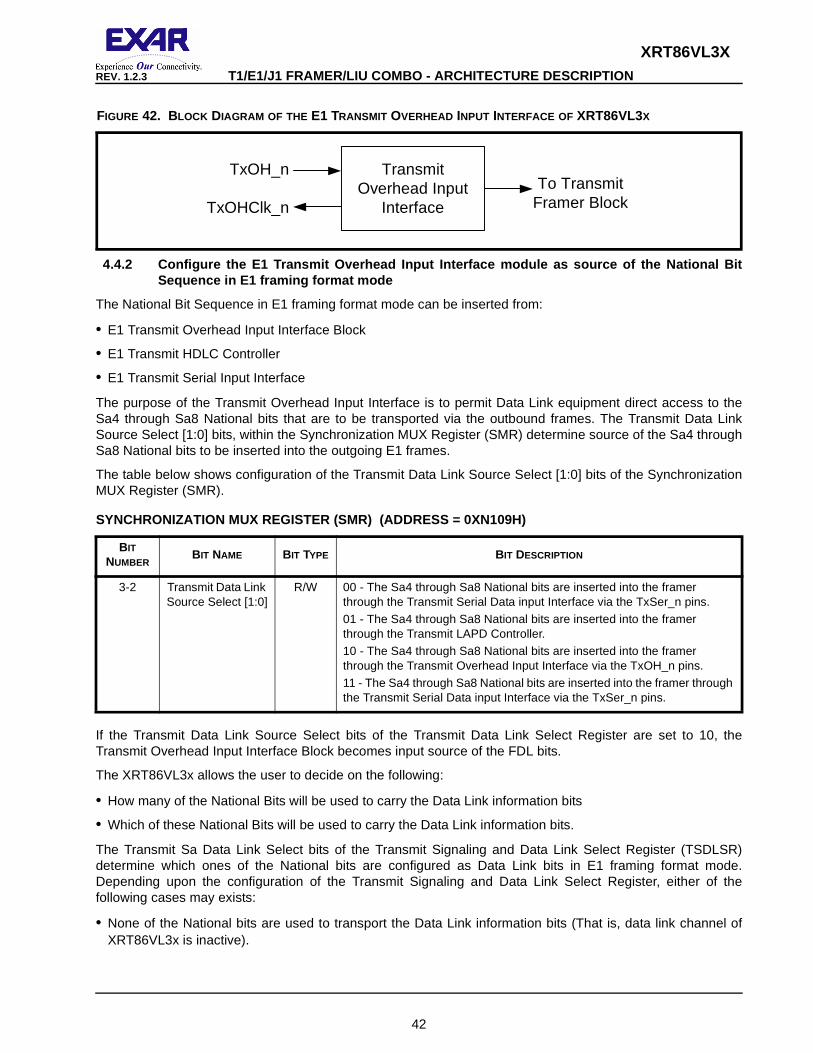
XRT86VL3X
42
REV. 1.2.3 T1/E1/J1 FRAMER/LIU COMBO - ARCHITECTURE DESCRIPTIO N
4.4.2 Configure the E1 Transmit Overhead Input Inter face module as source of the National BitSequence in E1 framing format mode
The National Bit Sequence in E1 framing format mode can be inserted from:
• E1 Transmit Overhead Input Interface Block
• E1 Transmit HDLC Controller
• E1 Transmit Serial Input Interface
The purpose of the Transmit Overhead Input Interface is to permit Data Link equipment direct access to theSa4 through Sa8 National bits that are to be transported via the outbound frames. The Transmit Data LinkSource Select [1:0] bits, within the Synchronization MUX Register (SMR) determine source of the Sa4 throughSa8 National bits to be inserted into the outgoing E1 frames.
The table below shows configuration of the Transmit Data Link Source Select [1:0] bits of the SynchronizationMUX Register (SMR).
If the Transmit Data Link Source Select bits of the Transmit Data Link Select Register are set to 10, theTransmit Overhead Input Interface Block becomes input source of the FDL bits.
The XRT86VL3x allows the user to decide on the following:
• How many of the National Bits will be used to carry the Data Link information bits
• Which of these National Bits will be used to carry the Data Link information bits.
The Transmit Sa Data Link Select bits of the Transmit Signaling and Data Link Select Register (TSDLSR)determine which ones of the National bits are configured as Data Link bits in E1 framing format mode.Depending upon the configuration of the Transmit Signaling and Data Link Select Register, either of thefollowing cases may exists:
• None of the National bits are used to transport the Data Link information bits (That is, data link channel ofXRT86VL3x is inactive).
FIGURE 42. BLOCK DIAGRAM OF THE E1 TRANSMIT OVERHEAD INPUT INTERFACE OF XRT86VL3X
SYNCHRONIZATION MUX REGISTER (SMR) (ADDRESS = 0XN109H)
BIT NUMBER
BIT NAME BIT TYPE BIT DESCRIPTION
3-2 Transmit Data Link Source Select [1:0]
R/W 00 - The Sa4 through Sa8 National bits are inserted into the framer through the Transmit Serial Data input Interface via the TxSer_n pins.
01 - The Sa4 through Sa8 National bits are inserted into the framer through the Transmit LAPD Controller.
10 - The Sa4 through Sa8 National bits are inserted into the framer through the Transmit Overhead Input Interface via the TxOH_n pins.
11 - The Sa4 through Sa8 National bits are inserted into the framer through the Transmit Serial Data input Interface via the TxSer_n pins.
TransmitOverhead Input
Interface
TxOH_n
TxOHClk_n
To TransmitFramer Block

XRT86VL3X
43
T1/E1/J1 FRAMER/LIU COMBO - ARCHITECTURE DESCRIPTIO N REV. 1.2.3
• Any combination of between 1 and all 5 of the National bits can be selected to transport the Data Linkinformation bits.
The table below shows configuration of the Transmit Sa Data Link Select bits of the Transmit Signaling andData Link Select Register (TSDLSR).
For every Sa bit that is selected to carry Data Link information, the Transmit Overhead Input Interface willsupply a clock pulse, via the TxOHClk_n output pin, such that:
• The Data Link equipment interfaced to the Transmit Overhead Input Interface should update the data on theTxOH_n line upon detection of the rising edge of TxOHClk_n.
• The Transmit Overhead Input Interface will sample and latch the data on the TxOH_n line on the falling edgeof TxOHClk_n.
TRANSMIT SIGNALING AND DATA LINK SELECT REGISTER (T SDLSR) (ADDRESS = 0XN10AH)
BIT NUMBER
BIT NAME BIT TYPE BIT DESCRIPTION
7 Transmit Sa8 Data Link Select
R/W 0 - Source of the Sa8 Nation bit is not from the data link interface.
1 - Source the Sa8 National bit from the data link interface.
6 Transmit Sa7 Data Link Select
R/W 0 - Source of the Sa7 Nation bit is not from the data link interface.
1 - Source the Sa7 National bit from the data link interface.
5 Transmit Sa6 Data Link Select
R/W 0 - Source of the Sa6 Nation bit is not from the data link interface.
1 - Source the Sa6 National bit from the data link interface.
4 Transmit Sa5 Data Link Select
R/W 0 - Source of the Sa5 Nation bit is not from the data link interface.
1 - Source the Sa5 National bit from the data link interface.
3 Transmit Sa4 Data Link Select
R/W 0 - Source of the Sa4 Nation bit is not from the data link interface.
1 - Source the Sa4 National bit from the data link interface.

XRT86VL3X
44
REV. 1.2.3 T1/E1/J1 FRAMER/LIU COMBO - ARCHITECTURE DESCRIPTIO N
Figure 43 below shows the timing diagram of the input and output signals associated with the E1 TransmitOverhead Input Interface module in E1 framing format mode.
FIGURE 43. E1 TRANSMIT OVERHEAD INPUT INTERFACE TIMING

XRT86VL3X
45
T1/E1/J1 FRAMER/LIU COMBO - ARCHITECTURE DESCRIPTIO N REV. 1.2.3
4.5 E1 Receive Overhead Interface
4.5.1 Description of the E1 Receive Overhead Output Interface Block
The E1 Receive Overhead Output Interface Block will allow an external device to be the consumer of the E1National bit sequence. This interface provides interface signals and required interface timing to shift out properdata link information at proper time.
The Receive Overhead Output Interface for a given Framer consists of two signals.
• RxOHClk_n: The Receive Overhead Output Interface Clock Output signal
• RxOH_n: The Receive Overhead Output Interface Output signal.
The Receive Overhead Output Interface Clock Output pin (RxOHCLK_n) generates a rising clock edge foreach National bit that is configured to carry Data Link information according to setting of the framer. The datalink bits extracted from the incoming E1 frames are outputted from the Receive Overhead Output InterfaceOutput pin (RxOH_n) before the rising edge of RxOHClk_n. The Data Link equipment should sample and latchthe data link bits at the rising edge of RxOHClk_n.
The figure below shows block diagram of the Receive Overhead Output Interface of XRT86VL3x.
4.5.2 Configure the E1 Receive Overhead Output Inter face module as source of the National BitSequence in E1 framing format mode
The National Bit Sequence in E1 framing format mode can be extracted and directed to:
• E1 Receive Overhead Output Interface Block
• E1 Receive HDLC Controller
• E1 Receive Serial Output Interface
The purpose of the Receive Overhead Output Interface is to permit Data Link equipment to have direct accessto the Sa4 through Sa8 National bits that are extracted from the incoming E1 frames. Independent of theavailability of the E1 Receive HDLC Controller module, the XRT86VL3x always output the received Nationalbits through the Receive Overhead Output Interface block.
The XRT86VL3x allows the user to decide on the following:
• How many of the National Bits is used to carry the Data Link information bits
• Which of these National Bits is used to carry the Data Link information bits.
The Receive Sa Data Link Select bits of the Receive Signaling and Data Link Select Register (TSDLSR)determine which ones of the National bits are configured as Data Link bits in E1 framing format mode.Depending upon the configuration of the Receive Signaling and Data Link Select Register, either of thefollowing cases may exists:
• None of the received National bits are used to transport the Data Link information bits (That is, data linkchannel of XRT86VL3x is inactive).
• Any combination of between 1 and all 5 of the received National bits are used to transport the Data Linkinformation bits.
FIGURE 44. BLOCK DIAGRAM OF THE E1 RECEIVE OVERHEAD OUTPUT INTERFACE OF XRT86VL3X
ReceiveOverhead Output
Interface
RxOH_n
RxOHClk_n
From ReceiveFramer Block

XRT86VL3X
46
REV. 1.2.3 T1/E1/J1 FRAMER/LIU COMBO - ARCHITECTURE DESCRIPTIO N
The table below shows configuration of the Receive Sa Data Link Select bits of the Receive Signaling and DataLink Select Register (RSDLSR).
For every received Sa bit that is determined to carry Data Link information, the Receive Overhead OutputInterface will supply a clock pulse, via the RxOHClk_n output pin, such that:
• The Receive Overhead Output interface should update the data on the RxOH_n line before the rising edge ofRxOHClk_n.
• The external Data Link equipment interfaced to the Receive Overhead Output Interface will sample and latchthe data on the RxOH_n line on the rising edge of RxOHClk_n.
Figure 45 below shows the timing diagram of the output signals associated with the E1 Receive OverheadOutput Interface module in E1 framing format mode.
RECEIVE SIGNALING AND DATA LINK SELECT REGISTER (RS DLSR) (ADDRESS = 0XN10CH)
BIT NUMBER
BIT NAME BIT TYPE BIT DESCRIPTION
7 Receive Sa8 Data Link Select
R/W 0 - The received Sa8 Nation bit is not extracted to the data link interface.
1 - The received Sa8 Nation bit is extracted to the data link interface.
6 Receive Sa7 Data Link Select
R/W 0 - The received Sa7 Nation bit is not extracted to the data link interface.
1 - The received Sa7 Nation bit is extracted to the data link interface.
5 Receive Sa6 Data Link Select
R/W 0 - The received Sa6 Nation bit is not extracted to the data link interface.
1 - The received Sa6 Nation bit is extracted to the data link interface.
4 Receive Sa5 Data Link Select
R/W 0 - The received Sa5 Nation bit is not extracted to the data link interface.
1 - The received Sa5 Nation bit is extracted to the data link interface.
3 Receive Sa4 Data Link Select
R/W 0 - The received Sa4 Nation bit is not extracted to the data link interface.
1 - The received Sa4 Nation bit is extracted to the data link interface.
FIGURE 45. E1 RECEIVE OVERHEAD OUTPUT INTERFACE TIMING

XRT86VL3X
47
T1/E1/J1 FRAMER/LIU COMBO - ARCHITECTURE DESCRIPTIO N REV. 1.2.3
5.0 LIU TRANSMIT PATH
5.1 Transmit Diagnostic Features
In addition to TAOS, the XRT86VL3x offers multiple diagnostic features for analyzing network integrity such asATAOS, Network Loop Code generation, and QRSS on a per channel basis by programming the appropriateregisters. These diagnostic features take priority over the digital data provided by the Framer block. Thetransmitters will send the diagnostic code to the line and will be maintained in the digital loopback if selected.
5.1.1 TAOS (Transmit All Ones)
The XRT86VL3x has the ability to transmit all ones on a per channel basis by programming the appropriatechannel register. This function takes priority over the digital data provided by the Framer block. For example:If a fixed "0011" pattern is provided by the Framer block and TAOS is enabled, the transmitter will output allones. Figure 46 is a diagram showing the all ones signal at TTIP and TRING.
5.1.2 ATAOS (Automatic Transmit All Ones)
If ATAOS is selected by programming the appropriate global register, an AMI all ones signal will be transmittedfor each channel that experiences an RLOS condition. If RLOS does not occur, the ATAOS will remain inactiveuntil an RLOS on a given channel occurs. A simplified block diagram of the ATAOS function is shown inFigure 47 .
5.1.3 Network Loop Up Code
By setting the LIU to generate a NLUC, the transmitters will send out a repeating "00001" pattern. The outputwaveform is shown in Figure 48 .
FIGURE 46. TAOS (TRANSMIT ALL ONES)
FIGURE 47. SIMPLIFIED BLOCK DIAGRAM OF THE ATAOS FUNCTION
TAOS
1 1 1
RLOSATAOS
TAOS
TTIP
TRINGTx

XRT86VL3X
48
REV. 1.2.3 T1/E1/J1 FRAMER/LIU COMBO - ARCHITECTURE DESCRIPTIO N
5.1.4 Network Loop Down Code
By setting the LIU to generate a NLDC, the transmitters will send out a repeating "001" pattern. The outputwaveform is shown in Figure 49 .
5.1.5 QRSS Generation
The XRT86VL3x can transmit a QRSS random sequence to a remote location from TTIP/TRING. Thepolynomial is shown in Table 3 .
5.2 T1 Long Haul Line Build Out (LBO)
The long haul transmitter output pulses are generated using a 7-Bit internal DAC (6-Bits plus the MSB sign bit).The line build out can be set to -7.5dB, -15dB, or -22dB cable attenuation by programming the appropriatechannel register. The long haul LBO consist of 32 discrete time segments extending over four consecutiveperiods of TCLK. As the LBO attenuation is increased, the pulse amplitude is reduced so that the waveformcomplies with ANSI T1.403 specifications. A long haul pulse with -7.5dB attenuation is shown in Figure 50 , apulse with -15dB attenuation is shown in Figure 51 , and a pulse with -22.5dB attenuation is shown inFigure 52 .
FIGURE 48. NETWORK LOOP UP CODE GENERATION
FIGURE 49. NETWORK LOOP DOWN CODE GENERATION
TABLE 3: RANDOM B IT SEQUENCE POLYNOMIALS
RANDOM PATTERN T1 E1
QRSS/PRBS 220 - 1 215 - 1
NetworkLoop-Up
Code
1 10 000 0 0 0 0 1
NetworkLoop-Down
Code
1 1 1 10 0 0 0 0 0 0

XRT86VL3X
49
T1/E1/J1 FRAMER/LIU COMBO - ARCHITECTURE DESCRIPTIO N REV. 1.2.3
FIGURE 50. LONG HAUL LINE BUILD OUT WITH -7.5DB ATTENUATION
FIGURE 51. LONG HAUL LINE BUILD OUT WITH -15DB ATTENUATION

XRT86VL3X
50
REV. 1.2.3 T1/E1/J1 FRAMER/LIU COMBO - ARCHITECTURE DESCRIPTIO N
FIGURE 52. LONG HAUL LINE BUILD OUT WITH -22.5DB ATTENUATION

XRT86VL3X
51
T1/E1/J1 FRAMER/LIU COMBO - ARCHITECTURE DESCRIPTIO N REV. 1.2.3
5.3 T1 Short Haul Line Build Out (LBO)
The short haul transmitter output pulses are generated using a 7-Bit internal DAC (6-Bit plus the MSB sign bit).The line build out can be set to interface to five different ranges of cable attenuation by programming theappropriate channel register. The pulse shape is divided into eight discrete time segments which are set tofixed values to comply with the pulse template. To program the eight segments individually to optimize aspecial line build out, see the arbitrary pulse section of this datasheet. The short haul LBO settings are shownin Table 4
5.3.1 Arbitrary Pulse Generator
The arbitrary pulse generator divides the pulse into eight individual segments. Each segment is set by a 7-Bitbinary word by programming the appropriate channel register. This allows the system designer to set theovershoot, amplitude, and undershoot for a unique line build out. The MSB (bit 7) is a sign-bit. If the sign-bit isset to "0", the segment will move in a positive direction relative to a flat line (zero) condition. If this sign-bit isset to "1", the segment will move in a negative direction relative to a flat line condition. The resolution of theDAC is typically 60mV per LSB. Thus, writing 7-bit = 1111111 will clamp the output at either voltage railcorresponding to a maximum amplitude. A pulse with numbered segments is shown in Figure 53 .
NOTE: By default, the arbitrary segments are programmed to 0x00h. The transmitter outputs will result in an all zeropattern to the line interface.
TABLE 4: SHORT HAUL LINE BUILD OUT
LBO SETTING EQC[4:0] R ANGE OF CABLE ATTENUATION
08h (01000) 0 - 133 Feet
09h (01001) 133 - 266 Feet
0Ah (01010) 266 - 399 Feet
0Bh (01011) 399 - 533 Feet
0Ch (01100) 533 - 655 Feet
FIGURE 53. ARBITRARY PULSE SEGMENT ASSIGNMENT
1
23
4
5
67
8
Segment Register
1 0x0Fn8 2 0x0Fn9 3 0x0Fna 4 0x0Fnb 5 0x0Fnc 6 0x0Fnd 7 0x0Fne 8 0x0Fnf

XRT86VL3X
52
REV. 1.2.3 T1/E1/J1 FRAMER/LIU COMBO - ARCHITECTURE DESCRIPTIO N
5.3.2 DMO (Digital Monitor Output)
The driver monitor circuit is used to detect transmit driver failures by monitoring the activities at TTIP/TRINGoutputs. Driver failure may be caused by a short circuit in the primary transformer or system problems at thetransmit inputs. If the transmitter of a channel has no output for more than 128 clock cycles, DMO goes "High"until a valid transmit pulse is detected. If the DMO interrupt is enabled, the change in status of DMO will causethe interrupt pin to go "Low". Once the status register is read, the interrupt pin will return "High" and the statusregister will be reset (RUR).
5.3.3 Transmit Jitter Attenuator
The transmit path has a dedicated jitter attenuator to reduce phase and frequency jitter in the transmit clock.The jitter attenuator uses a data FIFO (First In First Out) with a programmable depth of 32-bit or 64-bit. Whenthe Read and Write pointers of the FIFO are within 2-Bits of over-flowing or under-flowing, the bandwidth of thejitter attenuator is widened to track the short term input jitter, thereby avoiding data corruption. When thiscondition occurs, the jitter attenuator will not attenuate input jitter until the Read/Write pointer’s position isoutside the 2-Bit window. In T1 mode, the bandwidth of the JA is always set to 3Hz. In E1 mode, thebandwidth is programmable to either 10Hz or 1.5Hz (1.5Hz automatically selects the 64-Bit FIFO depth). TheJA has a clock delay equal to ½ of the FIFO bit depth.
NOTE: The Receive Path has a dedicated jitter attenuator. See the Receive Path Line Interface Section.
5.4 Line Termination (TTIP/TRING)
The output stage of the transmit path generates standard return-to-zero (RZ) signals to the line interface for T1/E1/J1 twisted pair or E1 coaxial cable. The physical interface is optimized by placing the terminatingimpedance inside the LIU. This allows one bill of materials for all modes of operation reducing the number ofexternal components necessary in system design. The transmitter outputs only require one DC blockingcapacitor of 0.68µF. For redundancy applications (or simply to tri-state the transmitters), set TxTSEL to a "1" inthe appropriate channel register. A typical transmit interface is shown in Figure 54 .
FIGURE 54. TYPICAL CONNECTION DIAGRAM USING INTERNAL TERMINATION
TTIP
TRING
XRT86VL3x LIU
1:2
Internal Impedance
Line Interface T1/E1/J1C=0.68uF
One Bill of Materials
TransmitterOutput

XRT86VL3X
53
T1/E1/J1 FRAMER/LIU COMBO - ARCHITECTURE DESCRIPTIO N REV. 1.2.3
6.0 LIU RECEIVE PATH
6.1 Line Termination (RTIP/RRING)
6.1.1 Internal Termination
The input stage of the receive path accepts standard T1/E1/J1 twisted pair or E1 coaxial cable inputs throughRTIP and RRING. The physical interface is optimized by placing the terminating impedance inside the LIU.This allows one bill of materials for all modes of operation reducing the number of external componentsnecessary in system design. The receive termination impedance is selected by programming TERSEL[1:0] tomatch the line impedance. Selecting the internal impedance is shown in Table 5 .
The XRT86VL3x has the ability to switch the internal termination to "High" impedance by programmingRxTSEL in the appropriate channel register, if the RxTSEL hardware pin is “High”. For internal termination, setRxTSEL to "1". By default, RxTSEL is set to "0" ("High" impedance). For redundancy applications, adedicated hardware pin (RxTSEL) is available to control the receive termination for all channelssimultaneously. This hardware pin is AND-ed with the register bit. Both, the register bit and the hardware pinmust be set active for the receiver to be configured for internal impedance. Figure 55 shows a typicalconnection diagram using the internal termination.
6.1.2 Equalizer Control
The main objective of the equalizer is to amplify an input attenuated signal to a pre-determined amplitude thatis acceptable to the peak detector circuit. Using feedback from the peak detector, the equalizer will gain theinput up to the maximum value specified by the equalizer control bits, in the appropriate channel register,normalizing the signal. Once the signal has reached the pre-determined amplitude, the signal is thenprocessed within the peak detector and slicer circuit. A simplified block diagram of the equalizer and peakdetector is shown in Figure 56 .
TABLE 5: SELECTING THE INTERNAL IMPEDANCE
TERSEL[1:0] R ECEIVE TERMINATION
0h (00) 100Ω
1h (01) 110Ω
2h (10) 75Ω
3h (11) 120Ω
FIGURE 55. TYPICAL CONNECTION DIAGRAM USING INTERNAL TERMINATION
RTIP
RRING
XRT86VL3x LIU1:1
Internal Impedance
Line Interface T1/E1/J1
One Bill of Materials
ReceiverInput
0.1µF

XRT86VL3X
54
REV. 1.2.3 T1/E1/J1 FRAMER/LIU COMBO - ARCHITECTURE DESCRIPTIO N
6.1.3 Cable Loss Indicator
The ability to monitor the cable loss attenuation of the receiver inputs is a valuable feature. The XRT86VL3xcontains a per channel, read only register for cable loss indication. CLOS[5:0] is a 6-Bit binary word thatreports the value of cable loss in 1dB steps with an absolute accuracy of ±1dB. An example of -25dB cableloss attenuation is shown in Figure 57 .
6.2 Receive Sensitivity
To meet Long Haul receive sensitivity requirements, the XRT86VL3x can accept T1/E1/J1 signals that havebeen attenuated by 43dB cable attenuation in E1 mode or 36dB cable attenuation in T1 mode withoutexperiencing bit errors, LOF, pattern synchronization, etc. Short haul specifications are for 12dB of flat loss inE1 mode. T1 specifications are 655 feet of cable loss along with 6dB of flat loss in T1 mode. The XRT86VL3xcan tolerate cable loss and flat loss beyond the industry specifications. The receive sensitivity in the short haulmode is approximately 4,000 feet without experiencing bit errors, LOF, pattern synchronization, etc. Althoughdata integrity is maintained, the RLOS function (if enabled) will report an RLOS condition according to thereceiver loss of signal section in this datasheet. The test configuration for measuring the receive sensitivity isshown in Figure .
FIGURE 56. SIMPLIFIED BLOCK DIAGRAM OF THE EQUALIZER AND PEAK DETECTOR
FIGURE 57. SIMPLIFIED BLOCK DIAGRAM OF THE CABLE LOSS INDICATOR
PeakDetector &
SlicerRx Equalizer
Rx EqualizerControl
RTIP
RRING
-25dB of Cable Loss
Equalizer and Peak Detector
CLOS[5:0] = 0x19h(25dec = 19hex)
-25dB Attenuated Signal
Read Only
XRT86VL3x

XRT86VL3X
55
T1/E1/J1 FRAMER/LIU COMBO - ARCHITECTURE DESCRIPTIO N REV. 1.2.3
6.2.1 AIS (Alarm Indication Signal)
The XRT86VL3x adheres to the ITU-T G.775 specification for an all ones pattern. The alarm indication signalis set to "1" if an all ones pattern (at least 99.9% ones density) is present for T, where T is 3ms to 75ms in T1mode. AIS will clear when the ones density is not met within the same time period T. In E1 mode, the AIS isset to "1" if the incoming signal has 2 or less zeros in a 512-bit window. AIS will clear when the incoming signalhas 3 or more zeros in the 512-bit window.
6.2.2 NLCD (Network Loop Code Detection)
The Network Loop Code Detection can be programmed to detect a Loop-Up, Loop-Down, or Automatic LoopCode. If the network loop code detection is programmed for Loop-Up, the NLCD will be set "High" if arepeating pattern of "00001" occurs for more than 5 seconds. If the network loop code detection isprogrammed for Loop-Down, the NLCD will be set "High" if a repeating pattern of "001" occurs for more than 5seconds. If the network loop code detection is programmed for automatic loop code, the LIU is configured todetect a Loop-Up code. If a Loop-Up code is detected for more than 5 seconds, the XRT86VL3x willautomatically program the channel into a remote loopback mode. The LIU will remain in remote loopback evenif the Loop-Up code disappears. The channel will continue in remote loop back until a Loop-Down code isdetected for more than 5 seconds (or, if the automatic loop code is disabled) and then automatically return tonormal operation with no loop back. The process of the automatic loop code detection is shown in Figure 59 .
FIGURE 58. TEST CONFIGURATION FOR MEASURING RECEIVE SENSITIVITY
Network Analyzer
E1 = PRBS 215 - 1T1 = PRBS 223 - 1
External Loopback
XRT86VL3xN-ChannelFramer/LIU
Cable Loss Flat LossTx
TxRx
Rx
W&G ANT20

XRT86VL3X
56
REV. 1.2.3 T1/E1/J1 FRAMER/LIU COMBO - ARCHITECTURE DESCRIPTIO N
6.2.3 FLSD (FIFO Limit Status Detection)
The purpose of the FIFO limit status is to indicate when the Read and Write FIFO pointers are within a pre-determined range (over-flow or under-flow indication). The FLSD is set to "1" if the FIFO Read and WritePointers are within ±3-Bits.
6.2.4 Receive Jitter Attenuator
The receive path has a dedicated jitter attenuator to reduce phase and frequency jitter in the recovered clock.The jitter attenuator uses a data FIFO (First In First Out) with a programmable depth of 32-bit or 64-bit. If theLIU is used for line synchronization (loop timing systems), the JA should be enabled in the receive path. Whenthe Read and Write pointers of the FIFO are within 2-Bits of over-flowing or under-flowing, the bandwidth of thejitter attenuator is widened to track the short term input jitter, thereby avoiding data corruption. When thiscondition occurs, the jitter attenuator will not attenuate input jitter until the Read/Write pointer’s position isoutside the 2-Bit window. In T1 mode, the bandwidth of the JA is always set to 3Hz. In E1 mode, thebandwidth is programmable to either 10Hz or 1.5Hz (1.5Hz automatically selects the 64-Bit FIFO depth). TheJA has a clock delay equal to ½ of the FIFO bit depth.
NOTE: The Transmit Path has a dedicated jitter attenuator. See the Transmit Path Line Interface Section.
6.2.5 RxMUTE (Receiver LOS with Data Muting)
The receive muting function can be selected by setting RxMUTE to "1" in the appropriate global register. Ifselected, any channel that experiences an RLOS condition will automatically pull the output of the LIU section"Low" to prevent data chattering. If RLOS does not occur, the RxMUTE will remain inactive until an RLOS on agiven channel occurs. The default setting for RxMUTE is "0" which is disabled. A simplified block diagram ofthe RxMUTE function is shown in Figure 60 .
FIGURE 59. PROCESS BLOCK FOR AUTOMATIC LOOP CODE DETECTION
Automatic RemoteLoopback
Loop-UpCode for5 sec?
Yes
No
Loop-DownCode for5 sec?
No Yes Disable RemoteLoopback

XRT86VL3X
57
T1/E1/J1 FRAMER/LIU COMBO - ARCHITECTURE DESCRIPTIO N REV. 1.2.3
FIGURE 60. SIMPLIFIED BLOCK DIAGRAM OF THE RXMUTE FUNCTION
RLOSRxMUTE
DigitalOutputLIU Framer

XRT86VL3X
58
REV. 1.2.3 T1/E1/J1 FRAMER/LIU COMBO - ARCHITECTURE DESCRIPTIO N
7.0 THE E1 TRANSMIT/RECEIVE FRAMER
7.1 Description of the Transmit/Receive Payload Data Input Interface Block
Each framer within the XRT86VL3x device includes a Transmit and Receive Payload Data Input Interfaceblock. Although most configurations are independent for the Tx and Rx path, once E1 framing has beenselected, both the Tx and Rx must operate in E1. The Payload Data Input Interface module (also known as theBack-plane Interface module) supports payload data to be taken from or presented to the system. In E1 mode,supported data rates are 2.048Mbit/s, MVIP 2.048Mbit/s, 4.096Mbit/s, 8.192Mbit/s, multiplexed 16.384Mbit/s,HMVIP 16.384Mbit/s, or H.100 16.384Mbit/s.
7.1.1 Brief Discussion of the Transmit/Receive Paylo ad Data Input Interface Block Operating atXRT84V24 Compatible 2.048Mbit/s mode
Whether or not the transmit/receive interface signals have been chosen as inputs or outputs, the overallsystem timing diagrams remain the same. It is the responsibility of the Terminal Equipment to provide serialinput data through the TxSER pin aligned with the Transmit Single-frame Synchronization signal and theTransmit Multi-frame Synchronization signal. Figure 61 shows how to connect the Transmit Payload DataInput Interface block to local Terminal Equipment. Figure 62 shows how to connect the Receive Payload DataOutput Interface to local Terminal Equipment.
FIGURE 61. INTERFACING THE TRANSMIT PATH TO LOCAL TERMINAL EQUIPMENT
TxSERCLK0
TxSER0
TxMSYNC0
TxSYNC0
TxCHCLK0
TxCHN[4:0]_0
TxSERCLKn
TxSERn
TxMSYNCn
TxSYNCn
TxCHCLKn
TxCHN[4:0]_n
TransmitPayload
Data InputInterfaceChn 0
TransmitPayload
Data InputInterfaceChn N
TerminalEquipment
XRT86VL3x
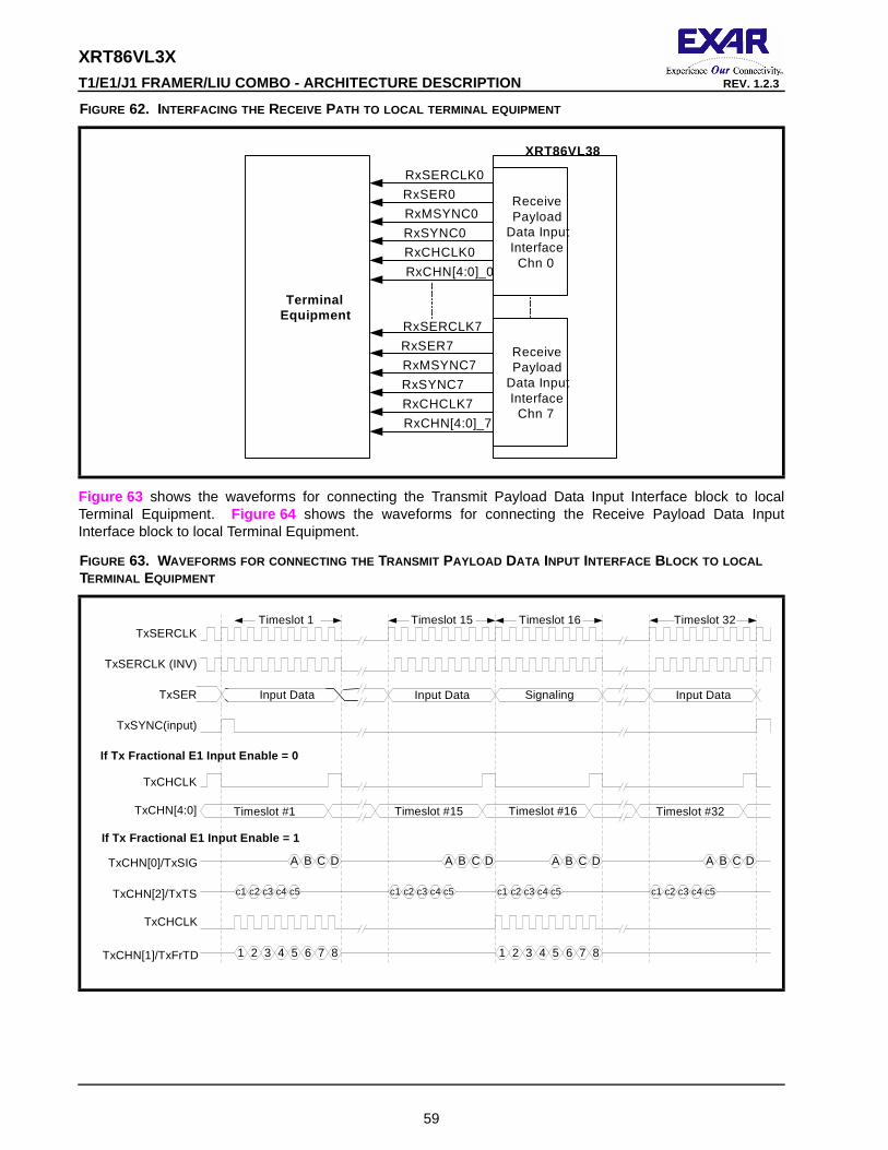
XRT86VL3X
59
T1/E1/J1 FRAMER/LIU COMBO - ARCHITECTURE DESCRIPTIO N REV. 1.2.3
Figure 63 shows the waveforms for connecting the Transmit Payload Data Input Interface block to localTerminal Equipment. Figure 64 shows the waveforms for connecting the Receive Payload Data InputInterface block to local Terminal Equipment.
FIGURE 62. INTERFACING THE RECEIVE PATH TO LOCAL TERMINAL EQUIPMENT
FIGURE 63. WAVEFORMS FOR CONNECTING THE TRANSMIT PAYLOAD DATA INPUT INTERFACE BLOCK TO LOCAL TERMINAL EQUIPMENT
RxSERCLK0
RxSER0
RxMSYNC0
RxSYNC0
RxCHCLK0
RxCHN[4:0]_0
RxSERCLK7
RxSER7
RxMSYNC7
RxSYNC7
RxCHCLK7
RxCHN[4:0]_7
ReceivePayload
Data InputInterface
Chn 0
ReceivePayload
Data InputInterface
Chn 7
TerminalEquipment
XRT86VL38
C
TxSERCLK
TxSERCLK (INV)
TxSER
TxSYNC(input)
TxCHCLK
TxCHN[4:0]
TxCHN[0]/TxSIG
TxCHCLK
TxCHN[2]/TxTS
TxCHN[1]/TxFrTD
c1 c2 c3 c4 c5 c1 c2 c3 c4 c5 c1 c2 c3 c4 c5 c1 c2 c3 c4 c5
87654321 87654321
Input Data Input Data Signaling Input Data
Timeslot #1 Timeslot #15 Timeslot #16 Timeslot #32
Timeslot 32Timeslot 1 Timeslot 15 Timeslot 16
A B D CA B D CA B DCA B D
If Tx Fractional E1 Input Enable = 0
If Tx Fractional E1 Input Enable = 1
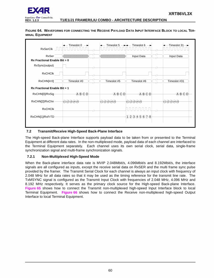
XRT86VL3X
60
REV. 1.2.3 T1/E1/J1 FRAMER/LIU COMBO - ARCHITECTURE DESCRIPTIO N
7.2 Transmit/Receive High-Speed Back-Plane Interface
The High-speed Back-plane Interface supports payload data to be taken from or presented to the TerminalEquipment at different data rates. In the non-multiplexed mode, payload data of each channel are interfaced tothe Terminal Equipment separately. Each channel uses its own serial clock, serial data, single-framesynchronization signal and multi-frame synchronization signals.
7.2.1 Non-Multiplexed High-Speed Mode
When the Back-plane interface data rate is MVIP 2.048Mbit/s, 4.096Mbit/s and 8.192Mbit/s, the interfacesignals are all configured as inputs, except the receive serial data on RxSER and the multi frame sync pulseprovided by the framer. The Transmit Serial Clock for each channel is always an input clock with frequency of2.048 MHz for all data rates so that it may be used as the timing reference for the transmit line rate. TheTxMSYNC signal is configured as the Transmit Input Clock with frequencies of 2.048 MHz, 4.096 MHz and8.192 MHz respectively. It serves as the primary clock source for the High-speed Back-plane Interface.Figure 65 shows how to connect the Transmit non-multiplexed high-speed Input Interface block to localTerminal Equipment. Figure 66 shows how to connect the Receive non-multiplexed high-speed OutputInterface to local Terminal Equipment.
FIGURE 64. WAVEFORMS FOR CONNECTING THE RECEIVE PAYLOAD DATA INPUT INTERFACE BLOCK TO LOCAL TER-MINAL EQUIPMENT
C
RxSerClk
RxSer
RxSync(output)
RxCHClk
RxCHN[4:0]
RxCHN[0]/RxSig
RxCHClk
RxCHN[2]/RxChn
RxCHN[1]/RxFrTD
c1 c2 c3 c4 c5 c1 c2 c3 c4 c5 c1 c2 c3 c4 c5 c1 c2 c3 c4 c5
87654321
A B D CA B D CA B DCA B D
Input Data Input Data
Timeslot 31Timeslot 0 Timeslot 5 Timeslot 6
Timeslot #0 Timeslot #5 Timeslot #6 Timeslot #31
Rx Fractional Enable Bit = 0
Rx Fractional Enable Bit = 1

XRT86VL3X
61
T1/E1/J1 FRAMER/LIU COMBO - ARCHITECTURE DESCRIPTIO N REV. 1.2.3
FIGURE 65. TRANSMIT NON-MULTIPLEXED HIGH-SPEED CONNECTION TO LOCAL TERMINAL EQUIPMENT USING MVIP 2.048MBIT/S, 4.096MBIT/S, OR 8.192MBIT/S
FIGURE 66. RECEIVE NON-MULTIPLEXED HIGH-SPEED CONNECTION TO LOCAL TERMINAL EQUIPMENT USING MVIP 2.048MBIT/S, 4.096MBIT/S, OR 8.192MBIT/S
TxSERCLK0
TxSER0
TxINCLK0
TxSYNC0
TransmitPayload
Data Input
InterfaceChn 0
TransmitPayload
Data Input
InterfaceChn 7
Terminal Equipment
XRT86VL38
TxSERCLK7
TxSER7
TxINCLK7
TxSYNC7
TxINCLK = 2.048/4.096/8.192MHz
RxSERCLK0
RxSER0
RxMSYNC0
RxSYNC0
ReceivePayload
Data Input
InterfaceChn 0
ReceivePayload
Data Input
InterfaceChn 7
Terminal Equipment
XRT86VL38
RxSERCLK7
RxSER7
RxMSYNC7
RxSYNC7
RxSERCLK = 2.048/4.096/8.192MHz

XRT86VL3X
62
REV. 1.2.3 T1/E1/J1 FRAMER/LIU COMBO - ARCHITECTURE DESCRIPTIO N
Figure 67 shows the waveforms for connecting the Transmit non-multiplexed high-speed Input Interface blockto local Terminal Equipment. Figure 68 shows the waveforms for connecting the Receive non-multiplexedhigh-speed Input Interface block to local Terminal Equipment.
FIGURE 67. WAVEFORMS FOR CONNECTING THE TRANSMIT NON-MULTIPLEXED HIGH-SPEED INPUT INTERFACE AT MVIP 2.048MBIT/S, 4.096MBIT/S, AND 8.192MBIT/S
FIGURE 68. WAVEFORMS FOR CONNECTING THE RECEIVE NON-MULTIPLEXED HIGH-SPEED INPUT INTERFACE AT MVIP 2.048MBIT/S, 4.096MBIT/S, AND 8.192MBIT/S
TxSERCLK
TxSERCLK (INV)
TxSER
TxSync(input)
TxSync(input)MVIP mode
TxCHCLK
TxCHN[0]/TxSig
TxSyncFrd=0
TxCHN[1]/TxFrTD
87654321 87654321 87654321 87654321
CA B DDon't Care CA B DDon't Care CA B DDon't Care CA B DDon't Care
Don't Care 87654321 Don't Care 87654321
Don't Care 87654321 Don't Care 87654321TxCHN[1]/TxFrTD
TxCHCLK
TxSyncFrd=1
87654321 87654321
CA B DDon't Care
TxMsync(2/4/8MHz)
RxSERCLK
RxSERCLK (INV)
RxSER
RxSync(input)
RxSync(input)MVIP mode
RxCHCLK
RxCHN[0]/RxSig
RxSyncFrd=0
RxCHN[1]/RxFrTD
87654321 87654321 87654321 87654321
CA B DDon't Care CA B DDon't Care CA B DDon't Care CA B DDon't Care
Don't Care 87654321 Don't Care 87654321
Don't Care 87654321 Don't Care 87654321RxCHN[1]/RxFrTD
RxCHCLK
RxSyncFrd=1
87654321 87654321
CA B DDon't Care
Timeslot 0 Timeslot 1 Timeslot 2 Timeslot 3 Timeslot 4 Timeslot 5
RxSERCLK(2/4/8MHz)
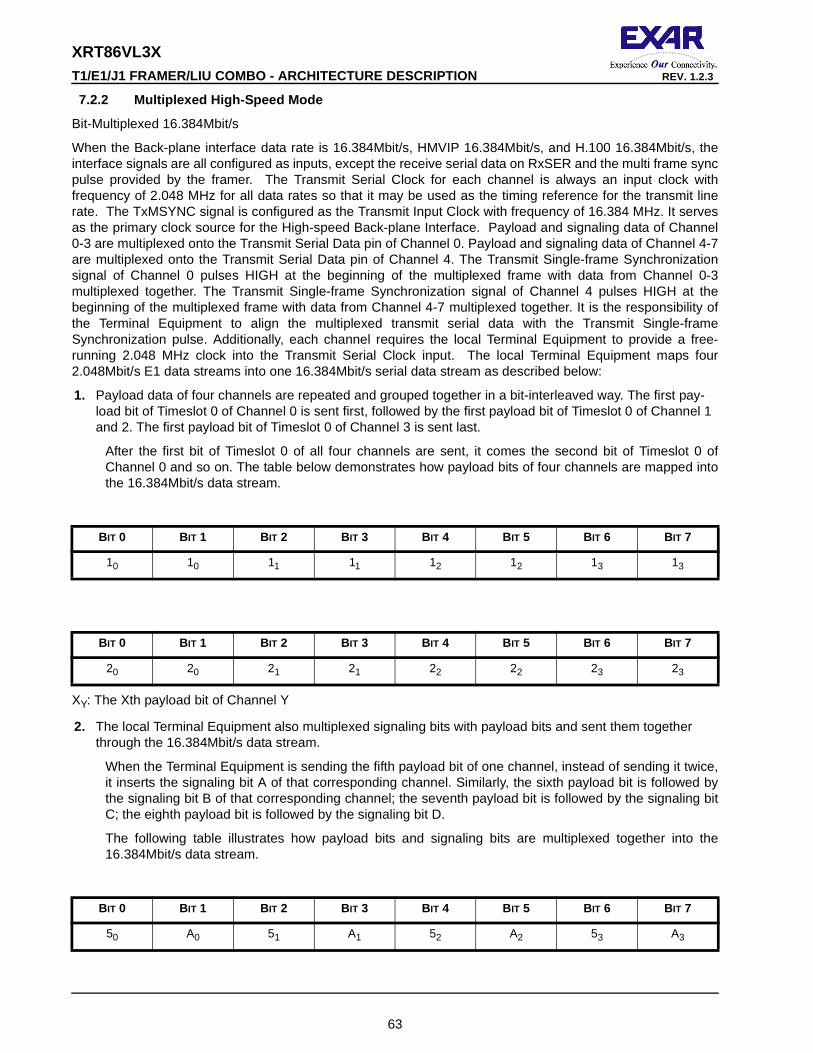
XRT86VL3X
63
T1/E1/J1 FRAMER/LIU COMBO - ARCHITECTURE DESCRIPTIO N REV. 1.2.3
7.2.2 Multiplexed High-Speed Mode
Bit-Multiplexed 16.384Mbit/s
When the Back-plane interface data rate is 16.384Mbit/s, HMVIP 16.384Mbit/s, and H.100 16.384Mbit/s, theinterface signals are all configured as inputs, except the receive serial data on RxSER and the multi frame syncpulse provided by the framer. The Transmit Serial Clock for each channel is always an input clock withfrequency of 2.048 MHz for all data rates so that it may be used as the timing reference for the transmit linerate. The TxMSYNC signal is configured as the Transmit Input Clock with frequency of 16.384 MHz. It servesas the primary clock source for the High-speed Back-plane Interface. Payload and signaling data of Channel0-3 are multiplexed onto the Transmit Serial Data pin of Channel 0. Payload and signaling data of Channel 4-7are multiplexed onto the Transmit Serial Data pin of Channel 4. The Transmit Single-frame Synchronizationsignal of Channel 0 pulses HIGH at the beginning of the multiplexed frame with data from Channel 0-3multiplexed together. The Transmit Single-frame Synchronization signal of Channel 4 pulses HIGH at thebeginning of the multiplexed frame with data from Channel 4-7 multiplexed together. It is the responsibility ofthe Terminal Equipment to align the multiplexed transmit serial data with the Transmit Single-frameSynchronization pulse. Additionally, each channel requires the local Terminal Equipment to provide a free-running 2.048 MHz clock into the Transmit Serial Clock input. The local Terminal Equipment maps four2.048Mbit/s E1 data streams into one 16.384Mbit/s serial data stream as described below:
1. Payload data of four channels are repeated and grouped together in a bit-interleaved way. The first pay-load bit of Timeslot 0 of Channel 0 is sent first, followed by the first payload bit of Timeslot 0 of Channel 1 and 2. The first payload bit of Timeslot 0 of Channel 3 is sent last.
After the first bit of Timeslot 0 of all four channels are sent, it comes the second bit of Timeslot 0 ofChannel 0 and so on. The table below demonstrates how payload bits of four channels are mapped intothe 16.384Mbit/s data stream.
XY: The Xth payload bit of Channel Y
2. The local Terminal Equipment also multiplexed signaling bits with payload bits and sent them together through the 16.384Mbit/s data stream.
When the Terminal Equipment is sending the fifth payload bit of one channel, instead of sending it twice,it inserts the signaling bit A of that corresponding channel. Similarly, the sixth payload bit is followed bythe signaling bit B of that corresponding channel; the seventh payload bit is followed by the signaling bitC; the eighth payload bit is followed by the signaling bit D.
The following table illustrates how payload bits and signaling bits are multiplexed together into the16.384Mbit/s data stream.
BIT 0 BIT 1 BIT 2 BIT 3 BIT 4 B IT 5 BIT 6 BIT 7
10 10 11 11 12 12 13 13
BIT 0 BIT 1 BIT 2 BIT 3 BIT 4 B IT 5 BIT 6 BIT 7
20 20 21 21 22 22 23 23
BIT 0 BIT 1 BIT 2 BIT 3 BIT 4 B IT 5 BIT 6 BIT 7
50 A0 51 A1 52 A2 53 A3

XRT86VL3X
64
REV. 1.2.3 T1/E1/J1 FRAMER/LIU COMBO - ARCHITECTURE DESCRIPTIO N
XY: The Xth payload bit of Channel Y
AY: The signaling bit A of Channel Y
3. After the first octet of all four channels are sent, the local Terminal Equipment start sending the second octets following the same rules of Step 1 and 2.
The Transmit Single-frame Synchronization signal of Channel 0 pulses HIGH for one clock cycle at the first bitposition of the multiplexed data stream with data from Channel 0-3 multiplexed together. The Transmit Single-frame Synchronization signal of Channel 4 pulses HIGH for one clock cycle at the first bit position of the datastream with data from Channel 4-7 multiplexed together. By sampling the HIGH pulse on the Transmit Single-frame Synchronization signal, the framer can position the beginning of the multiplexed E1 frame. It is theresponsibility of the Terminal Equipment to align the multiplexed transmit serial data with the Transmit Single-frame Synchronization pulse.
Inside the framer, all the "don't care" bits will be stripped away. The framing bits, signaling and payload data arede-multiplexed inside the XRT86VL3x device and send to each individual channel. These data will beprocessed by each individual framer and send to LIU interface. The local Terminal Equipment provides a free-running 2.048MHz clock to the Transmit Serial Input clock of each channel. The framer will use this clock tocarry the processed payload and signaling data to the transmit section of the device. Figure 69 shows how toconnect the Transmit multiplexed high-speed Input Interface block to local Terminal Equipment. Figure showsthe timing signals when framer is running at 16.384MHz Bit-Multiplexed mode.
HMVIP/ H100 16.384Mbit/s Byte-Multiplexed Mode
When the Transmit Multiplex Enable bit is set to one and the Transmit Interface Mode Select [1:0] bits are setto 10, the Transmit Back-plane interface of framer is running at HMVIP 16.384MHz. When Transmit InterfaceMode Select[1:0] bits are set to 11, the Transmit Back-plane interface is running at H100 16.384MHz mode.
The Transmit Back-plane Interface is accepting data through TxSer_0 or TxSer_4 pins at 16.384Mbit/s. Thelocal Terminal Equipment multiplexes payload data of every four channels into one data stream. Payload dataof Channel 0-3 are multiplexed onto the Transmit Serial Data pin of Channel 0. Payload data of Channel 4-7are multiplexed onto the Transmit Serial Data pin of Channel 4.
Free-running clocks of 16.384MHz is supplied to the Transmit Input Clock pin of Channel 0 and Channel 4 ofthe framer. The local Terminal Equipment provides multiplexed payload data at rising edge of this TransmitInput Clock. The Transmit High-speed Back-plane Interface of the framer then latches incoming serial data atfalling edge of the clock.
BIT 0 BIT 1 BIT 2 BIT 3 BIT 4 BIT 5 BIT 6 BIT 7
60 B0 61 B1 62 B2 63 B3
BIT 0 BIT 1 BIT 2 BIT 3 BIT 4 BIT 5 BIT 6 BIT 7
70 C0 71 C1 72 C2 73 C3
BIT 0 BIT 1 BIT 2 BIT 3 BIT 4 BIT 5 BIT 6 BIT 7
80 D0 81 D1 82 D2 83 D3
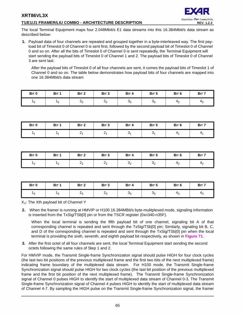
XRT86VL3X
65
T1/E1/J1 FRAMER/LIU COMBO - ARCHITECTURE DESCRIPTIO N REV. 1.2.3
The local Terminal Equipment maps four 2.048Mbit/s E1 data streams into this 16.384Mbit/s data stream asdescribed below:
1. Payload data of four channels are repeated and grouped together in a byte-interleaved way. The first pay-load bit of Timeslot 0 of Channel 0 is sent first, followed by the second payload bit of Timeslot 0 of Channel 0 and so on. After all the bits of Timeslot 0 of Channel 0 is sent repeatedly, the Terminal Equipment will start sending the payload bits of Timeslot 0 of Channel 1 and 2. The payload bits of Timeslot 0 of Channel 3 are sent last.
After the payload bits of Timeslot 0 of all four channels are sent, it comes the payload bits of Timeslot 1 ofChannel 0 and so on. The table below demonstrates how payload bits of four channels are mapped intoone 16.384Mbit/s data stream
XY: The Xth payload bit of Channel Y
2. When the framer is running at HMVIP or H100 16.384MBit/s byte-mulitplexed mode, signaling information is inserted from the TxSig/TSb[0] pin or from the TSCR register (0xn340-n35F).
When the local terminal is sending the fifth payload bit of one channel, signaling bit A of thatcorresponding channel is repeated and sent through the TxSig/TSb[0] pin; Similarly, signaling bit B, C,and D of the corresponding channel is repeated and sent through the TxSig/TSb[0] pin when the localterminal is providing the sixth, seventh, and eighth payload bit respectively, as shown in Figure 71 .
3. After the first octet of all four channels are sent, the local Terminal Equipment start sending the second octets following the same rules of Step 1 and 2.
For HMVIP mode, the Transmit Single-frame Synchronization signal should pulse HIGH for four clock cycles(the last two bit positions of the previous multiplexed frame and the first two bits of the next multiplexed frame)indicating frame boundary of the multiplexed data stream. For H100 mode, the Transmit Single-frameSynchronization signal should pulse HIGH for two clock cycles (the last bit position of the previous multiplexedframe and the first bit position of the next multiplexed frame). The Transmit Single-frame Synchronizationsignal of Channel 0 pulses HIGH to identify the start of multiplexed data stream of Channel 0-3. The TransmitSingle-frame Synchronization signal of Channel 4 pulses HIGH to identify the start of multiplexed data streamof Channel 4-7. By sampling the HIGH pulse on the Transmit Single-frame Synchronization signal, the framer
BIT 0 BIT 1 BIT 2 BIT 3 BIT 4 B IT 5 BIT 6 BIT 7
10 10 20 20 30 30 40 40
BIT 0 BIT 1 BIT 2 BIT 3 BIT 4 B IT 5 BIT 6 BIT 7
11 11 21 21 31 31 41 41
BIT 0 BIT 1 BIT 2 BIT 3 BIT 4 B IT 5 BIT 6 BIT 7
12 12 22 22 32 32 42 42
BIT 0 BIT 1 BIT 2 BIT 3 BIT 4 B IT 5 BIT 6 BIT 7
13 13 23 23 33 33 43 43

XRT86VL3X
66
REV. 1.2.3 T1/E1/J1 FRAMER/LIU COMBO - ARCHITECTURE DESCRIPTIO N
can position the beginning of the multiplexed E1 frame. It is responsibility of the Terminal Equipment to alignthe multiplexed transmit serial data with the Transmit Single-frame Synchronization pulse.
Inside the framer, all the "don't care" bits will be stripped away. The framing bits, signaling and payload data arede-multiplexed inside the XRT86VL3x device and send to each individual channel. These data will beprocessed by each individual framer and send to LIU interface. The local Terminal Equipment provides a free-running 2.048MHz clock to the Transmit Serial Input clock of each channel. The framer will use this clock tocarry the processed payload and signaling data to the transmit section of the device.
See Figure 69 below for how to interface the local Terminal Equipment with the Transmit Payload Data InputInterface block of the framer in HMVIP or H100 16.384Mbit/s mode. Figure 71 shows the timing signals whenthe framer is running at HMVIP or H100 16.384 MHz mode.
FIGURE 69. INTERFACING XRT86VL3X TRANSMIT TO LOCAL TERMINAL EQUIPMENT USING 16.384MBIT/S, HMVIP 16.384MBIT/S, AND H.100 16.384MBIT/S
FIGURE 70. TIMING SIGNAL WHEN THE FRAMER IS RUNNING AT BIT-MULTIPLEXED 16.384MBIT/S MODE
TxSER0
TxINCLK0 (16.384MHz)
TxSYNC0
TxSERCLK0 (2.048MHz)
TransmitPayload
Data InputInterface
Chn 0
TransmitPayload
Data InputInterface
Chn 4
Terminal Equipment
XRT86VL38
Chn 1
Chn 2
Chn 3
Chn 5
Chn 6
Chn 7
TxSERCLK1 (2.048MHz)
TxSERCLK2 (2.048MHz)
TxSERCLK3 (2.048MHz)
TxSER4
TxINCLK4 (16.384MHz)
TxSYNC4
TxSERCLK4 (2.048MHz)
TxSERCLK5 (2.048MHz)
TxSERCLK6 (2.048MHz)
TxSERCLK7 (2.048MHz)
TxInClk (16.384MHz)
TxInClk (INV)
TxSer
TxSync(input)
10 X 11 X X X12 13 20 X 21 X X30 40 X 50 A0 51 A1 52 A2 53 A3
56 cyclesh0 X h1 X X Xh2 h3
8-bit header
XRT86VL3X
67
T1/E1/J1 FRAMER/LIU COMBO - ARCHITECTURE DESCRIPTIO N REV. 1.2.3
E1 Receive Multiplexed Mode
The interface consists of the following pins:
• Data Output (RxSer_n)
• Receive Serial Clock Input signal (RxSerClk_n)
• Receive Single-frame Synchronization Input signal (RxSync_n)
The Receive Back-plane Interface is pumping out data through RxSer_0 or RxSer_4 pins at 16.384Mbit/s. Itmultiplexes payload and signaling data of every four channels into one data stream. Payload and signalingdata of Channel 0-3 are multiplexed onto the Receive Serial Data pin of Channel 0. Payload and signaling dataof Channel 4-7 are multiplexed onto the Receive Serial Data pin of Channel 4.
Free-running clocks of 16.384MHz are supplied to the Receive Serial Clock pin of Channel 0 and Channel 4 ofthe framer. The Receive High-speed Back-plane Interface of the farmer provides data at rising edge of thisReceive Serial Clock. The local Terminal Equipment then latches incoming serial data at falling edge of theclock. Figure 72 shows the interface of the Recieve Payload Data Output Interface Block to the TerminalEquipment.
The multiplexed data output on RxSER_0 or RxSER_4 are very similar to the Multiplexed data input onTxSER_0 or TxSER_4 except when the receive framer is running at 16MHz Bit-Multiplexed mode. When thereceive framer is running at 16MHz Bit-Multiplexed mode, the multiplexed data on RxSER_0 or RxSER_4 arereturn-to-zero data when the receive framer is processing the first four bits of each time slot data of eachchannel, as shown in Figure . Figure shows the timing signal when the receive framer is running at HMVIP orH.100 16.384 MHz mode.
FIGURE 71. WAVEFORMS FOR CONNECTING THE TRANSMIT MULTIPLEXED HIGH-SPEED INPUT INTERFACE AT HMVIP AND H.100 16.384MBIT/S MODE
TxInClk (16.384MHz)
TxInClk (INV)
TxSer 1212 52 5210 10 20 20 30 4030 40 50 50 60 6073 73 83 83 h0 h0h0 h0 h0 h0 h0 h0
56 cycles53 53 63 63 73 73 83 83
00 A2A20 0 0 0 0 A00 A0 B0B0C3C3D3D3 1 11 1 1 1 1 156 cycles
A3A3B3B3C3C3D3D3TxSig
TxSync(input)HMVIP, negative sync
TxSync(input)HMVIP, positive sync
Start of Frame Xy : X is the bit number and y is the channel number
TxSync(input)H.100, negative sync
TxSync(input)H.100, positive sync
Delayer H.100
TxSync(input)H.100, negative sync
TxSync(input)H.100, positive sync
00

XRT86VL3X
68
REV. 1.2.3 T1/E1/J1 FRAMER/LIU COMBO - ARCHITECTURE DESCRIPTIO N
FIGURE 72. INTERFACING XRT86VL3X RECEIVE TO LOCAL TERMINAL EQUIPMENT USING 16.384MBIT/S, HMVIP 16.384MBIT/S, AND H.100 16.384MBIT/S
FIGURE 73. TIMING SIGNAL WHEN THE RECEIVE FRAMER IS RUNNING AT 16.384MHZ BIT-MULITPLEXED MODE
FIGURE 74. TIMING SIGNAL WEHN THE RECEIVE FRAMER IS RUNNING AT HMVIP AND H100 16.384MHZ MODE
RxSER0
RxSERCLK0 (12/16MHz)
RxSYNC0
TransmitPayload
Data InputInterface
Chn 0
TransmitPayload
Data InputInterface
Chn 4
TerminalEquipment
XRT86VL38
Chn 1
Chn 2
Chn 3
Chn 5
Chn 6
Chn 7
RxSER4
RxSERCLK (12/16MHz)
RxSYNC4
RxSerClk (16.384MHz)
RxSerClk (INV)
RxSer
RxSync(input)
10 0 11 0 0 012 13 20 0 21 0 030 40 0 50 A0 51 A1 52 A2 53 A3
56 cyclesh0 X h1 X X Xh2 h3
8-bit header
RxSerClk (16.384MHz)
RxSerClk (INV)
RxSer 1212 52 5210 10 20 20 30 4030 40 50 50 60 6073 73 83 83 h0 h1h0 h1 h2 h2 h3 h3
56 cycles53 53 63 63 73 73 83 83
00 A2A20 0 0 0 0 00 0 A0A0B0B0C3C3D3D3 1 11 1 1 1 1 156 cycles
A3A3B3B3C3C3D3D3RxSig
Start of Frame Xy : X is the bit number and y is the channel number
RxSync(input)H.100, negative sync
RxSync(input)H.100, positive sync
RxSync(input)HMVIP, negative sync
RxSync(input)HMVIP, positive sync

XRT86VL3X
69
T1/E1/J1 FRAMER/LIU COMBO - ARCHITECTURE DESCRIPTIO N REV. 1.2.3
7.3 Brief Discussion of Common Channel Signaling in E1 Framing Format
As the name referred, Common Channel Signaling is signaling information common to all thirty voice or datachannels of an E1 trunk. Time slot 16 may be used to carry Common Channel Signaling data of up to a rate of64kbits/s. The national bits of time slot 0 may also be used for Common Channel Signaling. Since there arefive national bits of time slot 0 per every two E1 frames, the total bandwidth of the national bits is 20kbits/s. TheCommon Channel Signaling is essentially data link information that provides performance monitoring and atransmission quality report.
7.4 Brief Discussion of Channel Associated Signaling in E1 Framing Format
Signaling is required when dealing with voice and dial-up data services in E1 applications. Traditionally,signaling is provided on a dial-up telephone line across the talk-path. Signaling is used to tell the receiverwhere the call or route is destined. The signal is sent through switches along the route to a distant end.Common types of signals are:
• On hook
• Off hook
• Dial tone
• Dialed digits
• Ringing cycle
• Busy tone
A signal is consists of four bits namely A, B, C and D. These bits define the state of the call for a particular timeslot. Time slot 16 of each E1 frame can carry CAS signals for two E1 voice or data channels. Therefore,sixteen E1 frames are needed to carry CAS signals for all 32 E1 channels. The sixteen E1 frames then formsa CAS Multi-frame.
7.5 Insert/Extract Signaling Bits from TSCR Register
The four most significant bits of the Transmit Signaling Control Register (TSCR) of each time slot can be usedto store outgoing signaling data. The user can program these bits through microprocessor access. If theXRT86VL3x framer is configure to insert signaling bits from TSCR registers, the E1 Transmit Framer block willfill up the time slot 16 octet with the signaling bits stored inside the TSCR registers. The insertion of signalingbit into PCM data is done on a per-channel basis. The most significant bit (Bit 7) of TSCR register is used tostore Signaling bit A. Bit 6 is used to hold Signaling bit B. Bit 5 is used to hold Signaling bit C. Bit 4 is used tohold Signaling bit D.
7.6 Insert/Extract Signaling Bits from TxCHN[0]_n/Tx SIG Pin
The XRT86VL3x framer can be configured to insert/extract signaling bits provided by external equipmentthrough the external signaling bus. When the Fractional E1 mode is enabled, this bus is configured as TxSIGand RxSIG. These pins act as an the signaling bus for the outbound E1 frames.
Figure 75 shows a timing diagram of the TxSIG input pin. Figure 76 shows a timing diagram of the RxSIGoutput pin. Please note that the Signaling Bit A of a certain channel coincides with Bit 5 of the PCM data of thatchannel; Signaling Bit B coincides with Bit 6 of the PCM data; Signaling Bit C coincides with Bit 7 of the PCMdata and Signaling Bit D coincides with Bit 8 (LSB) of the PCM data.

XRT86VL3X
70
REV. 1.2.3 T1/E1/J1 FRAMER/LIU COMBO - ARCHITECTURE DESCRIPTIO N
7.7 Enable Channel Associated Signaling and Signalin g Data Source Control
The Transmit Signaling Control Register (TSCR) of each channel selects source of signaling data to beinserted into the outgoing E1 frame and enables Channel Associated signaling. As we mentioned before, thesignaling data can be inserted from Transmit Signaling Control Registers (TSCR) of each timeslot, from theTxSig_n input pin, from the TxOH_n input pin or from the TxSer_n input pin. The Transmit Signaling DataSource Select [1:0] bits of the Transmit Signaling Control Register (TSCR) determines from which sources thesignaling data is inserted from.
FIGURE 75. TIMING DIAGRAM OF THE TXSIG INPUT
FIGURE 76. TIMING DIAGRAM OF THE RXSIG OUTPUT

XRT86VL3X
71
T1/E1/J1 FRAMER/LIU COMBO - ARCHITECTURE DESCRIPTIO N REV. 1.2.3
8.0 THE DS1 TRANSMIT/RECEIVE FRAMER
8.1 Description of the Transmit/Receive Payload Data Input Interface Block
Each of the four framers within the XRT86VL3x device includes a Transmit and Receive Payload Data InputInterface block. Although most configurations are independent for the Tx and Rx path, once T1 framing hasbeen selected, both the Tx and Rx must operate in T1. The Payload Data Input Interface module (also knownas the Back-plane Interface module) supports payload data to be taken from or presented to the system. In T1modes, supported data rates are 1.544Mbit/s, MVIP 2.048Mbit/s, 4.096Mbit/s, 8.192Mbit/s, multiplexed12.352Mbit/s, 16.384Mbit/s, HMVIP 16.384Mbit/s, or H.100 16.384Mbit/s.
8.1.1 Brief Discussion of the Transmit/Receive Paylo ad Data Input Interface Block Operating at1.544Mbit/s mode
Whether or not the transmit/receive interface signals have been chosen as inputs or outputs, the overallsystem timing diagrams remain the same. It is the responsibility of the Terminal Equipment to provide serialinput data through the TxSER pin aligned with the Transmit Single-frame Synchronization signal and theTransmit Multi-frame Synchronization signal. Figure 77 shows how to connect the Transmit Payload DataInput Interface block to local Terminal Equipment. Figure 78 shows how to connect the Receive Payload DataOutput Interface to local Terminal Equipment.
FIGURE 77. INTERFACING THE TRANSMIT PATH TO LOCAL TERMINAL EQUIPMENT
TxSERCLK0
TxSER0
TxMSYNC0
TxSYNC0
TxCHCLK0
TxCHN[4:0]_0
TxSERCLKn
TxSERn
TxMSYNCn
TxSYNCn
TxCHCLKn
TxCHN[4:0]_n
TransmitPayload
Data InputInterface
Chn 0
TransmitPayload
Data InputInterfaceChn N
TerminalEquipment
XRT86VL3x
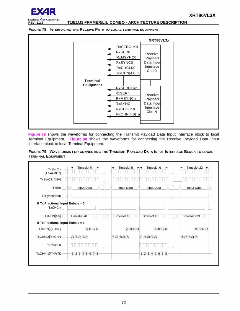
XRT86VL3X
72
REV. 1.2.3 T1/E1/J1 FRAMER/LIU COMBO - ARCHITECTURE DESCRIPTIO N
Figure 79 shows the waveforms for connecting the Transmit Payload Data Input Interface block to localTerminal Equipment. Figure 80 shows the waveforms for connecting the Receive Payload Data InputInterface block to local Terminal Equipment.
FIGURE 78. INTERFACING THE RECEIVE PATH TO LOCAL TERMINAL EQUIPMENT
FIGURE 79. WAVEFORMS FOR CONNECTING THE TRANSMIT PAYLOAD DATA INPUT INTERFACE BLOCK TO LOCAL TERMINAL EQUIPMENT
RxSERCLK0
RxSER0
RxMSYNC0
RxSYNC0
RxCHCLK0
RxCHN[4:0]_0
RxSERCLKn
RxSERn
RxMSYNCn
RxSYNCn
RxCHCLKn
RxCHN[4:0]_n
ReceivePayload
Data InputInterface
Chn 0
ReceivePayload
Data InputInterfaceChn N
TerminalEquipment
XRT86VL3x
C
TxSerClk (1.544MHz)
TxSerClk (INV)
TxSer
TxSync(input)
TxCHClk
TxCHN[4:0]
TxCHN[0]/TxSig
TxCHCLK
TxCHN[2]/TxCHN
TxCHN[1]/TxFrTD
F F
c1 c2 c3 c4 c5 c1 c2 c3 c4 c5 c1 c2 c3 c4 c5 c1 c2 c3 c4 c5
87654321 87654321
Input Data Input Data Input Data Input Data
Timeslot #0 Timeslot #5 Timeslot #6 Timeslot #23
Timeslot 23Timeslot 0 Timeslot 5 Timeslot 6
A B D CA B D CA B DCA B D
If Tx Fractional Input Enbale = 0
If Tx Fractional Input Enbale = 1
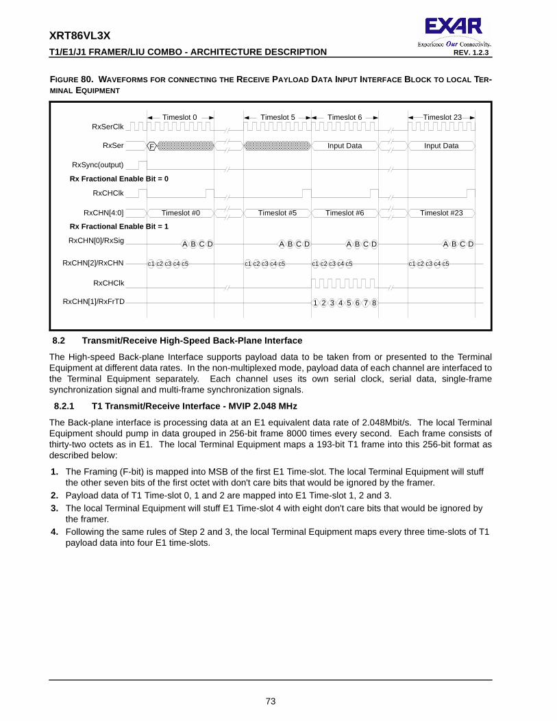
XRT86VL3X
73
T1/E1/J1 FRAMER/LIU COMBO - ARCHITECTURE DESCRIPTIO N REV. 1.2.3
8.2 Transmit/Receive High-Speed Back-Plane Interface
The High-speed Back-plane Interface supports payload data to be taken from or presented to the TerminalEquipment at different data rates. In the non-multiplexed mode, payload data of each channel are interfaced tothe Terminal Equipment separately. Each channel uses its own serial clock, serial data, single-framesynchronization signal and multi-frame synchronization signals.
8.2.1 T1 Transmit/Receive Interface - MVIP 2.048 MHz
The Back-plane interface is processing data at an E1 equivalent data rate of 2.048Mbit/s. The local TerminalEquipment should pump in data grouped in 256-bit frame 8000 times every second. Each frame consists ofthirty-two octets as in E1. The local Terminal Equipment maps a 193-bit T1 frame into this 256-bit format asdescribed below:
1. The Framing (F-bit) is mapped into MSB of the first E1 Time-slot. The local Terminal Equipment will stuff the other seven bits of the first octet with don't care bits that would be ignored by the framer.
2. Payload data of T1 Time-slot 0, 1 and 2 are mapped into E1 Time-slot 1, 2 and 3.3. The local Terminal Equipment will stuff E1 Time-slot 4 with eight don't care bits that would be ignored by
the framer.4. Following the same rules of Step 2 and 3, the local Terminal Equipment maps every three time-slots of T1
payload data into four E1 time-slots.
FIGURE 80. WAVEFORMS FOR CONNECTING THE RECEIVE PAYLOAD DATA INPUT INTERFACE BLOCK TO LOCAL TER-MINAL EQUIPMENT
C
RxSerClk
RxSer
RxSync(output)
RxCHClk
RxCHN[4:0]
RxCHN[0]/RxSig
RxCHClk
RxCHN[2]/RxCHN
RxCHN[1]/RxFrTD
c1 c2 c3 c4 c5 c1 c2 c3 c4 c5 c1 c2 c3 c4 c5 c1 c2 c3 c4 c5
87654321
A B D CA B D CA B DCA B D
Input Data Input Data
Timeslot 23Timeslot 0 Timeslot 5 Timeslot 6
Timeslot #0 Timeslot #5 Timeslot #6 Timeslot #23
Rx Fractional Enable Bit = 0
Rx Fractional Enable Bit = 1
F

XRT86VL3X
74
REV. 1.2.3 T1/E1/J1 FRAMER/LIU COMBO - ARCHITECTURE DESCRIPTIO N
The mapping of T1 frame into E1 framing format is shown in the table below.
8.2.2 Non-Multiplexed High-Speed Mode
When the Back-plane interface data rate is MVIP 2.048Mbit/s, 4.096Mbit/s and 8.192Mbit/s, the interfacesignals are all configured as inputs, except the receive serial data on RxSER and the multi frame sync pulse(RxMSYNC) provided by the framer. The Transmit Serial Clock for each channel is always an input clock withfrequency of 1.544 MHz for all data rates so that it may be used as the timing reference for the transmit linerate. The TxMSYNC signal is configured as the Transmit Input Clock with frequencies of 2.048 MHz, 4.096MHz and 8.192 MHz respectively. It serves as the primary clock source for the High-speed Back-planeInterface. Figure 81 shows how to connect the Transmit non-multiplexed high-speed Input Interface block tolocal Terminal Equipment. Figure 82 shows how to connect the Receive non-multiplexed high-speed OutputInterface to local Terminal Equipment.
TABLE 6: MAPPING A T1 FRAME INTO AN E1 FRANE
T1 F-Bit TS0 TS1 TS2 Don't Care Bits TS3 TS4 TS5
E1 TS0 TS1 TS2 TS3 TS4 TS5 TS6 TS7
T1 Don't Care Bits TS6 TS7 TS8 Don't Care Bits TS9 TS10 TS11
E1 TS8 TS9 TS10 TS11 TS12 TS13 TS14 TS15
T1 Don't Care Bits TS12 TS13 TS14 Don't Care Bits TS15 TS16 TS17
E1 TS16 TS17 TS18 TS19 TS20 TS21 TS22 TS23
T1 Don't Care Bits TS18 TS19 TS20 Don't Care Bits TS21 TS22 TS23
E1 TS24 TS25 TS26 TS27 TS28 TS29 TS30 TS31
FIGURE 81. TRANSMIT NON-MULTIPLEXED HIGH-SPEED CONNECTION TO LOCAL TERMINAL EQUIPMENT USING MVIP 2.048MBIT/S, 4.096MBIT/S, OR 8.192MBIT/S
TxSERCLK0
TxSER0
TxINCLK0
TxSYNC0
TransmitPayload
Data InputInterfaceChn 0
TransmitPayload
Data InputInterfaceChn N
TerminalEquipment
XRT86VL3x
TxSERCLKn
TxSERn
TxINCLKn
TxSYNCn
TxINCLK = 2.048/4.096/8.192MHz
XRT86VL3X
75
T1/E1/J1 FRAMER/LIU COMBO - ARCHITECTURE DESCRIPTIO N REV. 1.2.3
Figure 83 shows the waveforms for connecting the Transmit non-multiplexed high-speed Input Interface blockto local Terminal Equipment. Figure 84 shows the waveforms for connecting the Receive non-multiplexedhigh-speed Input Interface block to local Terminal Equipment.
FIGURE 82. RECEIVE NON-MULTIPLEXED HIGH-SPEED CONNECTION TO LOCAL TERMINAL EQUIPMENT USING MVIP 2.048MBIT/S, 4.096MBIT/S, OR 8.192MBIT/S
FIGURE 83. WAVEFORMS FOR CONNECTING THE TRANSMIT NON-MULTIPLEXED HIGH-SPEED INPUT INTERFACE AT MVIP 2.048MBIT/S, 4.096MBIT/S, AND 8.192MBIT/S
RxSERCLK0
RxSER0
RxMSYNC0
RxSYNC0
ReceivePayload
Data InputInterface
Chn 0
ReceivePayload
Data InputInterfaceChn N
TerminalEquipment
XRT86VL3x
RxSERCLKn
RxSERn
RxMSYNCn
RxSYNCn
RxSERCLK = 2.048/4.096/8.192MHz
TxSERCLK(1.5 MHz)
TxSERCLK (INV)
TxSER
TxSYNC(input)
TxCHCLK(INV)
TxCHN[0]/TxSig
TxCHN[1]/TxFrTD
F 87654321 87654321 87654321 87654321
CA B DDon't Care CA B DDon't Care CA B DDon't Care Don't Care CA B DDon't Care
Note: The following signals are not aligned with the signals shown above. The TxTSClk is derived from 1.544MHz transmit clock.
Don't Care 87654321 Don't Care 87654321
TxMSYNC(2/4/8MHz)
Don't Care Don't care

XRT86VL3X
76
REV. 1.2.3 T1/E1/J1 FRAMER/LIU COMBO - ARCHITECTURE DESCRIPTIO N
8.2.3 Multiplexed High-Speed Mode
When the Back-plane interface data rate is 12.352Mbit/s, 16.384Mbit/s, HMVIP 16.384Mbit/s, and H.10016.384Mbit/s, the interface signals are all configured as inputs, except the receive serial data on RxSER andthe multi frame sync pulse provided by the framer. The Back-plane Interface is processing data throughTxSER0 or TxSER4 pins at 12.352Mbit/s or 16.384Mbit/s. The local Terminal Equipment multiplexes payloadand signaling data of every four channels into one serial data stream. Payload and signaling data of Channel 0-3 are multiplexed onto the Transmit Serial Data pin of Channel 0. Payload and signaling data of Channel 4-7are multiplexed onto the Transmit Serial Data pin of Channel 4. Free-running clocks of 12.352MHz aresupplied to the Transmit Input Clock pin of Channel 0 and Channel 4 of the framer. The local TerminalEquipment provides multiplexed payload data at rising edge of this Transmit Input Clock. The Transmit High-speed Back-plane Interface of the framer then latches incoming serial data at falling edge of the clock.
Transmit 12.352 Bit-Multiplexed Mode
The local Terminal Equipment maps four 1.544Mbit/s DS1 data streams into one 12.352Mbit/s serial datastream as described below:
1. The F-bit of four channels are repeated and grouped together to form the first octet of the multiplexed data stream. The F-bit of Channel 0 is sent first, followed by F-bit of Channel 1 and 2. The F-bit of Channel 3 is sent last. The table below shows bit-pattern of the first octet.
FX: F-bit of Channel X
2. Payload data of four channels are repeated and grouped together in a bit-interleaved way. The first pay-load bit of Timeslot 0 of Channel 0 is sent first, followed by the first payload bit of Timeslot 0 of Channel 1 and 2. The first payload bit of Timeslot 0 of Channel 3 is sent last. After the first bits of Timeslot 0 of all four
FIGURE 84. WAVEFORMS FOR CONNECTING THE RECEIVE NON-MULTIPLEXED HIGH-SPEED INPUT INTERFACE AT MVIP 2.048MBIT/S, 4.096MBIT/S, AND 8.192MBIT/S
BIT PATTERN OF THE FIRST OCTET
BIT 0 BIT 1 BIT 2 BIT 3 BIT 4 BIT 5 BIT 6 BIT 7
F0 F0 F1 F1 F2 F2 F3 F3
RxSER
RxSYNC(input)
RxCHCLK(INV)
RxCHN[0]/RxSig
RxCHN[1]/RxFrTD
F 87654321 87654321 87654321 87654321
CA B DDon't Care CA B DDon't Care CA B DDon't Care CA B DDon't Care
Note: The following signals are not aligned with the signals shown above. The RxTSClk is derived from 1.544MHz transmit clock.
Don't Care 87654321 Don't Care 87654321
Don't Care Don't care
Don't care
RxSERCLK(2/4/8MHz)

XRT86VL3X
77
T1/E1/J1 FRAMER/LIU COMBO - ARCHITECTURE DESCRIPTIO N REV. 1.2.3
channels are sent, it comes the second bit of Timeslot 0 of Channel 0 and so on. The table below demon-strates how payload bits of four channels are mapped into the 12.352Mbit/s data stream.
XY: The Xth payload bit of Channel Y
3. The local Terminal Equipment also multiplexes signaling bits with payload bits and sends them together through the 12.352Mbit/s data stream. When the Terminal Equipment is sending the fifth payload bit of each channel, instead of sending it twice, it inserts the signaling bit A of that corresponding channel. Simi-larly, the sixth payload bit of a each channel is followed by the signaling bit B of that channel; the seventh payload bit is followed by the signaling bit C; the eighth payload bit is followed by the signaling bit D.
The following table illustrates how payload bits and signaling bits are multiplexed together into the 12.352Mbit/s data stream.
XY: The Xth payload bit of Channel Y
AY: The signaling bit A of Channel Y
4. Following the same rules of Step 2 and 3, the local Terminal Equipment continues to map the payload data and signaling data of four channels into a 12.352Mbit/s data stream.
BIT 0 BIT 1 BIT 2 BIT 3 BIT 4 B IT 5 BIT 6 BIT 7
10 10 11 11 12 12 13 13
BIT 0 BIT 1 BIT 2 BIT 3 BIT 4 B IT 5 BIT 6 BIT 7
20 20 21 21 22 22 23 23
BIT 0 BIT 1 BIT 2 BIT 3 BIT 4 B IT 5 BIT 6 BIT 7
50 A0 51 A1 52 A2 53 A3
BIT 0 BIT 1 BIT 2 BIT 3 BIT 4 B IT 5 BIT 6 BIT 7
60 B0 61 B1 62 B2 63 B3
BIT 0 BIT 1 BIT 2 BIT 3 BIT 4 B IT 5 BIT 6 BIT 7
70 C0 71 C1 72 C2 73 C3
BIT 0 BIT 1 BIT 2 BIT 3 BIT 4 B IT 5 BIT 6 BIT 7
80 D0 81 D1 82 D2 83 D3
XRT86VL3X
78
REV. 1.2.3 T1/E1/J1 FRAMER/LIU COMBO - ARCHITECTURE DESCRIPTIO N
The Transmit Single-frame Synchronization signal of Channel 0 pulses HIGH for one clock cycle at the first bitposition (F-bit of channel 0) of the multiplexed data stream with data from Channel 0-3 multiplexed together.The Transmit Single-frame Synchronization signal of Channel 4 pulses HIGH for one clock cycle at the first bitposition (F-bit of Channel 4) of the data stream with data from Channel 4-7 multiplexed together. By samplingthe HIGH pulse on the Transmit Single-frame Synchronization signal, the framer can position the beginning ofthe multiplexed DS1 frame. It is responsibility of the Terminal Equipment to align the multiplexed transmit serialdata with the Transmit Single-frame Synchronization pulse.
Inside the framer, all the "don't care" bits will be stripped away. The framing bits, signaling and payload data arede-multiplexed inside the XRT86VL3x and sent to each individual channel. These data will be processed byeach individual framer and send to the LIU interface. The local Terminal Equipment provides a free-running1.544MHz clock to the Transmit Serial Input clock of each channel. The framer will use this clock to carry theprocessed payload and signaling data to the transmit section of the device. Figure 85 shows how to connectthe Transmit multiplexed high-speed Input Interface block to local Terminal Equipment. Figure 89 shows thetiming signal when the transmit framer is running at 12.352 Bit-Multiplexed Mode
FIGURE 85. INTERFACING XRT86VL3X TRANSMIT TO LOCAL TERMINAL EQUIPMENT USING 16.384MBIT/S, HMVIP 16.384MBIT/S, AND H.100 16.384MBIT/S
TxSER0TxINCLK0 (12/16MHz)
TxSYNC0
TxSERCLK0 (1.544MHz)
TransmitPayload
Data InputInterfaceChn 0
TransmitPayload
Data InputInterfaceChn 4
TerminalEquipment
XRT86VL38
Chn 1
Chn 2
Chn 3
Chn 5
Chn 6
Chn 7
TxSERCLK1 (1.544MHz)
TxSERCLK2 (1.544MHz)
TxSERCLK3 (1.544MHz)
TxSER4TxINCLK4 (12/16MHz)
TxSYNC4
TxSERCLK4 (1.544MHz)
TxSERCLK5 (1.544MHz)
TxSERCLK6 (1.544MHz)
TxSERCLK7 (1.544MHz)
XRT86VL3X
79
T1/E1/J1 FRAMER/LIU COMBO - ARCHITECTURE DESCRIPTIO N REV. 1.2.3
Transmit 16.384 Bit-Multiplexed Mode
Please refer to Figure 85 for how to interface the transmit payload data input interface block to the terminalequipment. The local Terminal Equipment maps four 1.544Mbit/s DS1 data streams into this 16.384Mbit/s datastream as described below:
1. The F-bit of four channels are repeated and grouped together to form the first octet of the multiplexed data stream. The F-bit of Channel 0 is sent first, followed by F-bit of Channel 1 and 2. The F-bit of Channel 3 is sent last. The table below shows bit-pattern of the first octet.
FX: F-bit of Channel X
2. After the first octet of data is sent, the local Terminal Equipment should insert seven octets (fifty-six bits) of "don't care" data into the outgoing data stream.
3. Payload data of four channels are repeated and grouped together in a bit-interleaved way. The first pay-load bit of Timeslot 0 of Channel 0 is sent first, followed by the first payload bit of Timeslot 0 of Channel 1 and 2. The first payload bit of Timeslot 0 of Channel 3 is sent last. After the first bits of Timeslot 0 of all four channels are sent, it comes the second bit of Timeslot 0 of Channel 0 and so on. The table below demon-strates how payload bits of four channels are mapped into the 16.384Mbit/s data stream.
XY: The Xth payload bit of Channel Y
4. The local Terminal Equipment also multiplexed signaling bits with payload bits and sent them together through the 16.384Mbit/s data stream. When the Terminal Equipment is sending the fifth payload bit of each channel, instead of sending it twice, it inserts the signaling bit A of that corresponding channel. Simi-larly, the sixth payload bit of each channel is followed by the signaling bit B of that channel; the seventh payload bit is followed by the signaling bit C; the eighth payload bit is followed by the signaling bit D.
FIGURE 86. TIMING SIGNALS WHEN THE TRANSMIT FRAMER IS RUNNING AT 12.352 B IT-MULTIPLEXED MODE
BIT 0 BIT 1 BIT 2 BIT 3 BIT 4 B IT 5 BIT 6 BIT 7
F0 F0 F1 F1 F2 F2 F3 F3
BIT 0 BIT 1 BIT 2 BIT 3 BIT 4 B IT 5 BIT 6 BIT 7
10 10 11 11 12 12 13 13
BIT 0 BIT 1 BIT 2 BIT 3 BIT 4 B IT 5 BIT 6 BIT 7
20 20 21 21 22 22 23 23
TxInClk (12.352MHz)
TxInClk (INV)
TxSer
TxSync(input)
F0 F0 F1 F1 F2 F2 F3 F3 10 X 11 X X X12 13 20 X 21 X X30 40 X 50 A0 51 A1 52 A2 53 A3 60 B0 61 B1 62 B2 63 B3
XRT86VL3X
80
REV. 1.2.3 T1/E1/J1 FRAMER/LIU COMBO - ARCHITECTURE DESCRIPTIO N
The following table illustrates how payload bits and signaling bits are multiplexed together into the 16.384Mbit/s data stream.
XY: The Xth payload bit of Channel Y
AY: The signaling bit A of Channel Y
5. After payload bits of Timeslot 0, 1 and 2 of all four channels are sent, the Terminal Equipment should stuff another eight octets (sixty-four bits) of "don't care" data into the outgoing data stream.
6. Following the same rules of Step 2 to 5, the local Terminal Equipment stuffs eight octets of "don't care" data after sending twenty-four octets of multiplexed payload and signaling data. A 16.384Mbit/s data stream is thus created.
The Transmit Single-frame Synchronization signal of Channel 0 pulses HIGH for one clock cycle at the first bitposition (F-bit of channel 0) of the data stream with data from Channel 0-3 multiplexed together. The TransmitSingle-frame Synchronization signal of Channel 4 pulses HIGH for one clock cycle at the first bit position (F-bitof Channel 4) of the data stream with data from Channel 4-7 multiplexed together. By sampling the HIGH pulseon the Transmit Single-frame Synchronization signal, the framer can position the beginning of the multiplexedDS1 frame. It is responsibility of the Terminal Equipment to align the multiplexed transmit serial data with theTransmit Single-frame Synchronization pulse.
Inside the framer, all the "don't care" bits will be stripped away. The framing bits, signaling and payload data arede-multiplexed inside the XRT86VL3x and send to each individual channel. These data will be processed byeach individual framer and send to LIU interface. The local Terminal Equipment provides a free-running1.544MHz clock to the Transmit Serial Input clock of each channel. The framer will use this clock to carry theprocessed payload and signaling data to the transmit section of the device.
Figure shows the timing signal when the transmit framer is running at 16.384 Bit-Multiplexed mode.
BIT 0 BIT 1 BIT 2 BIT 3 BIT 4 BIT 5 BIT 6 BIT 7
50 A0 51 A1 52 A2 53 A3
BIT 0 BIT 1 BIT 2 BIT 3 BIT 4 BIT 5 BIT 6 BIT 7
60 B0 61 B1 62 B2 63 B3
BIT 0 BIT 1 BIT 2 BIT 3 BIT 4 BIT 5 BIT 6 BIT 7
70 C0 71 C1 72 C2 73 C3
BIT 0 BIT 1 BIT 2 BIT 3 BIT 4 BIT 5 BIT 6 BIT 7
80 D0 81 D1 82 D2 83 D3

XRT86VL3X
81
T1/E1/J1 FRAMER/LIU COMBO - ARCHITECTURE DESCRIPTIO N REV. 1.2.3
Transmit HMVIP / H.100 Byte-Multiplexed mode at 16. 384 MHz
Please refer to Figure 85 for how to interface the transmit payload data input interface block to the terminalequipment. The local Terminal Equipment maps four 1.544Mbit/s DS1 data streams into this 16.384Mbit/s datastream as described below:
1. The F-bit of four channels are repeated and grouped together to form the first octet of the multiplexed data stream. The F-bit of Channel 0 is sent first, followed by F-bit of Channel 1 and 2. The F-bit of Channel 3 is sent last. The table below shows bit-pattern of the first octet.
FX: F-bit of Channel X
2. After the first octet of data is sent, the local Terminal Equipment should insert seven octets (fifty-six bits) of "don't care" data into the outgoing data stream.
3. Payload data of four channels are repeated and grouped together in a byte-interleaved way. The first pay-load bit of Timeslot 0 of Channel 0 is sent first, followed by the second payload bit of Timeslot 0 of Channel 0 and so on. After all the bits of Timeslot 0 of Channel 0 is sent repeatedly, the Terminal Equipment will start sending the payload bits of Timeslot 0 of Channel 1 and 2. The payload bits of Timeslot 0 of Channel 3 are sent the last. After the payload bits of Timeslot 0 of all four channels are sent, it comes the payload bits of Timeslot 1 of Channel 0 and so on. The table below demonstrates how payload bits of four channels are mapped into the 16.384Mbit/s data stream.
FIGURE 87. TIMING SIGNALS WHEN THE TRANSMIT FRAMER IS RUNNING AT 16.384 BIT-MULTIPLEXED MODE
BIT 0 BIT 1 BIT 2 BIT 3 BIT 4 B IT 5 BIT 6 BIT 7
F0 F0 F1 F1 F2 F2 F3 F3
BIT 0 BIT 1 BIT 2 BIT 3 BIT 4 B IT 5 BIT 6 BIT 7
10 10 20 20 30 30 40 40
BIT 0 BIT 1 BIT 2 BIT 3 BIT 4 B IT 5 BIT 6 BIT 7
11 11 21 21 31 31 41 41
BIT 0 BIT 1 BIT 2 BIT 3 BIT 4 B IT 5 BIT 6 BIT 7
12 12 22 22 32 32 42 42
TxInClk (16.384MHz)
TxInClk (INV)
TxSer
TxSync(input)
F0 F0 F1 F1 F2 F2 F3 F3 10 X 11 X X X12 13 20 X 21 X X30 40 X 50 A0 51 A1 52 A2 53 A3
56 cycles

XRT86VL3X
82
REV. 1.2.3 T1/E1/J1 FRAMER/LIU COMBO - ARCHITECTURE DESCRIPTIO N
XY: The Xth payload bit of Channel Y
4. When the framer is running at HMVIP 16.384MBit/s byte-mulitplexed mode, signaling information is inserted from the TxSig/TxCHN[0] pin or from the TSCR register (0xn340-n357). When the local terminal is sending the fifth payload bit of one channel, signaling bit A of that corresponding channel is repeated and sent through the TxSig/TxCHN[0] pin; Similarly, signaling bit B, C, and D of the corresponding channel is repeated and sent through the TxSig/TxCHN[0] pin when the local terminal is providing the sixth, sev-enth, and eighth payload bit respectively, as shown in Figure .
5. After payload bits of Timeslot 0, 1 and 2 of all four channels are sent, the Terminal Equipment should stuff another eight octets (sixty-four bits) of "don't care" data into the outgoing data stream.
6. Following the same rules of Step 2 to 5, the local Terminal Equipment stuffs eight octets of "don't care" data after sending twenty-four octets of multiplexed payload and signaling data. A 16.384Mbit/s data stream is thus created.
For HMVIP mode, the Transmit Single-frame Synchronization signal should pulse HIGH for four clock cycles(the last two bit positions of the previous multiplexed frame and the first two bits of the next multiplexed frame)indicating frame boundary of the multiplexed data stream. For H.100 mode, TxSYNC should pulse HIGH fortwo clock cycles (the last bit position of the previous multiplexed frame and the first bit of the next multiplexedframe). The Transmit Single-frame Synchronization signal of Channel 0 pulses HIGH to identify the start ofmultiplexed data stream of Channel 0-3. The Transmit Single-frame Synchronization signal of Channel 4pulses HIGH to identify the start of multiplexed data stream of Channel 4-7. By sampling the HIGH pulse on theTransmit Single-frame Synchronization signal, the framer can position the beginning of the multiplexed DS1frame. It is responsibility of the Terminal Equipment to align the multiplexed transmit serial data with theTransmit Single-frame Synchronization pulse.
Inside the framer, all the "don't care" bits will be stripped away. The framing bits, signaling and payload data arede-multiplexed inside the XRT86VL3x and send to each individual channel. These data will be processed byeach individual framer and send to LIU interface. The local Terminal Equipment provides a free-running1.544MHz clock to the Transmit Serial Input clock of each channel. The framer will use this clock to carry theprocessed payload and signaling data to the transmit section of the device.
BIT 0 BIT 1 BIT 2 BIT 3 BIT 4 BIT 5 BIT 6 BIT 7
13 13 23 23 33 33 43 43
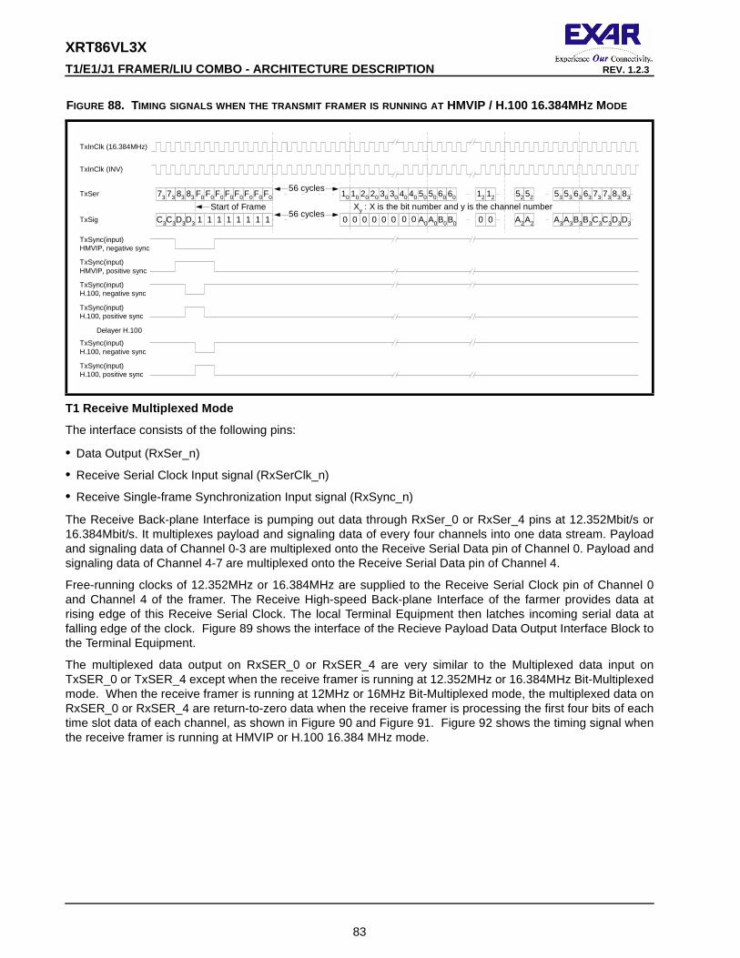
XRT86VL3X
83
T1/E1/J1 FRAMER/LIU COMBO - ARCHITECTURE DESCRIPTIO N REV. 1.2.3
T1 Receive Multiplexed Mode
The interface consists of the following pins:
• Data Output (RxSer_n)
• Receive Serial Clock Input signal (RxSerClk_n)
• Receive Single-frame Synchronization Input signal (RxSync_n)
The Receive Back-plane Interface is pumping out data through RxSer_0 or RxSer_4 pins at 12.352Mbit/s or16.384Mbit/s. It multiplexes payload and signaling data of every four channels into one data stream. Payloadand signaling data of Channel 0-3 are multiplexed onto the Receive Serial Data pin of Channel 0. Payload andsignaling data of Channel 4-7 are multiplexed onto the Receive Serial Data pin of Channel 4.
Free-running clocks of 12.352MHz or 16.384MHz are supplied to the Receive Serial Clock pin of Channel 0and Channel 4 of the framer. The Receive High-speed Back-plane Interface of the farmer provides data atrising edge of this Receive Serial Clock. The local Terminal Equipment then latches incoming serial data atfalling edge of the clock. Figure 89 shows the interface of the Recieve Payload Data Output Interface Block tothe Terminal Equipment.
The multiplexed data output on RxSER_0 or RxSER_4 are very similar to the Multiplexed data input onTxSER_0 or TxSER_4 except when the receive framer is running at 12.352MHz or 16.384MHz Bit-Multiplexedmode. When the receive framer is running at 12MHz or 16MHz Bit-Multiplexed mode, the multiplexed data onRxSER_0 or RxSER_4 are return-to-zero data when the receive framer is processing the first four bits of eachtime slot data of each channel, as shown in Figure 90 and Figure 91. Figure 92 shows the timing signal whenthe receive framer is running at HMVIP or H.100 16.384 MHz mode.
FIGURE 88. TIMING SIGNALS WHEN THE TRANSMIT FRAMER IS RUNNING AT HMVIP / H.100 16.384MHZ MODE
TxInClk (16.384MHz)
TxInClk (INV)
TxSer 1212 52 5210 10 20 20 30 4030 40 50 50 60 6073 73 83 83 F0 F0F0 F0 F0 F0 F0 F0
56 cycles53 53 63 63 73 73 83 83
00 A2A20 0 0 0 0 A00 A0 B0B0C3C3D3D3 1 11 1 1 1 1 156 cycles
A3A3B3B3C3C3D3D3TxSig
TxSync(input)HMVIP, negative sync
TxSync(input)HMVIP, positive sync
Start of Frame Xy : X is the bit number and y is the channel number
TxSync(input)H.100, negative sync
TxSync(input)H.100, positive sync
Delayer H.100
TxSync(input)H.100, negative sync
TxSync(input)H.100, positive sync
00

XRT86VL3X
84
REV. 1.2.3 T1/E1/J1 FRAMER/LIU COMBO - ARCHITECTURE DESCRIPTIO N
.
FIGURE 89. INTERFACING XRT86VL3X RECEIVE TO LOCAL TERMINAL EQUIPMENT USING 16.384MBIT/S, HMVIP 16.384MBIT/S, AND H.100 16.384MBIT/S
FIGURE 90. WAVEFORMS FOR CONNECTING THE RECEIVE MULTIPLEXED HIGH-SPEED INPUT INTERFACE AT 12.352MBIT/S MODE
FIGURE 91. WAVEFORMS FOR CONNECTING THE RECEIVE MULTIPLEXED HIGH-SPEED INPUT INTERFACE AT 16.384MBIT/S MODE
RxSER0
RxSERCLK0 (12/16MHz)
RxSYNC0
TransmitPayload
Data InputInterfaceChn 0
TransmitPayload
Data InputInterfaceChn 4
TerminalEquipment
XRT86VL38
Chn 1
Chn 2
Chn 3
Chn 5
Chn 6
Chn 7
RxSER4
RxSERCLK (12/16MHz)
RxSYNC4
RxSerClk (12.352MHz)
RxSerClk (INV)
RxSer
RxSync(input)
F0 F0 F1 F1 F2 F2 F3 F3 10 0 11 0 0 012 13 20 0 21 0 030 40 0 50 A0 51 A1 52 A2 53 A3 60 B0 61 B1 62 B2 63 B3
RxSerClk (16.384MHz)
RxSerClk (INV)
RxSer
RxSync(input)
F0 F0 F1 F1 F2 F2 F3 F3 10 0 11 0 0 012 13 20 0 21 0 030 40 0 50 A0 51 A1 52 A2 53 A3
56 cycles

XRT86VL3X
85
T1/E1/J1 FRAMER/LIU COMBO - ARCHITECTURE DESCRIPTIO N REV. 1.2.3
8.3 Brief Discussion of Robbed-bit Signaling in DS1 Framing Format
Signaling is required when dealing with voice and dial-up data services in DS1 applications. Traditionally,signaling is provided on a dial-up telephone line, across the talk-path. Bit robbing, or stealing the leastsignificant bit (8th bit) in each of the twenty-four voice channels in the signaling frames allows enough bits tosignal between the transmitting and receiving end. That is where the name Robbed-bit signaling comes from.These ends can be CPE to central office (CO) for switched services, or CPE to CPE for PBX-to-PBXconnections.
Signaling is used to tell the receiver where the call or route is destined. The signal is sent through switchesalong the route to a distant end. Common types of signals are:
• On hook
• Off hook
• Dial tone
• Dialed digits
• Ringing cycle
• Busy tone
Robbed-bit Signaling is supported in three DS1 framing formats.
• Super-Frame (SF)
• SLC®96
• Extended Super-Frame (ESF)
In Super-Frame or SLC®96 framing mode, frame number 6 and frame number 12 are signaling frames. Inchannelized DS1 applications, these frames are used to contain the signaling information. In frame number 6and 12, the least significant bit of all twenty-four timeslots is 'robbed' to carry call state information. The bit inframe 6 is called the A bit and the bit in frame 12 is called the B bit. The combination of A and B defines thestate of the call for the particular timeslot that these two bits are located in.
FIGURE 92. WAVEFORMS FOR CONNECTING THE RECEIVE MULTIPLEXED HIGH-SPEED INPUT INTERFACE AT HMVIP AND H.100 16.384MBIT/S MODE
RxSerClk (16.384MHz)
RxSerClk (INV)
RxSer 1212 52 5210 10 20 20 30 4030 40 50 50 60 6073 73 83 83 F0 F1F0 F1 F2 F2 F3 F3
56 cycles53 53 63 63 73 73 83 83
00 A2A20 0 0 0 0 00 0 A0A0B0B0C3C3D3D3 1 11 1 1 1 1 156 cycles
A3A3B3B3C3C3D3D3RxSig
Start of Frame Xy : X is the bit number and y is the channel number
RxSync(input)H.100, negative sync
RxSync(input)H.100, positive sync
RxSync(input)HMVIP, negative sync
RxSync(input)HMVIP, positive sync

XRT86VL3X
86
REV. 1.2.3 T1/E1/J1 FRAMER/LIU COMBO - ARCHITECTURE DESCRIPTIO N
In Extended Super-Frame framing mode, frame number 6, 12, 18 and 24 are signaling frames. In theseframes, the least significant bit of all twenty-four timeslots is 'robbed' to carry call state information. The bit inframe 6 is called the A bit, the bit in frame 12 is called the B bit, the bit in frame 18 is called the C bit and the bitin frame 24 is called the D bit. The combination of A, B, C and D defines the state of the call for the particulartimeslot that these signaling bits are located in.
8.3.1 Configure the framer to transmit Robbed-bit Si gnaling
The XRT86VL3x framer supports transmission of Robbed-bit Signaling in ESF, SF and SLC®96 framingformats. Signaling bits can be inserted into the outgoing DS1 frame through the following:
• Signaling data is inserted from Transmit Signaling Control Registers (TSCR) of each timeslot
• Signaling data is inserted from TxSig_n pin
• Signaling data is embedded into the input PCM data coming from the Terminal Equipment
8.3.2 Insert Signaling Bits from TSCR Register
The four most significant bits of the Transmit Signaling Control Register (TSCR) of each timeslot can be usedto store outgoing signaling data. The user can program these bits through the microprocessor access. If theXRT86VL3x framer is configured to insert signaling bits from the TSCR registers, the DS1 Transmit Framerblock will strip off the least significant bits of each time slot in the signaling frames and replace it with thesignaling bit stored inside the TSCR registers. The insertion of signaling bits into PCM data is done on a per-channel basis.
In SF or SLC®96 mode, the user can control the XRT86VL3x framer to transmit no signaling (transparent),two-code signaling, or four-code signaling. Two-code signaling is done by substituting the least significant bit(LSB) of the specific channel in frame 6 and 12 with the content of the Signaling bit A of the specific TSCRregister.
Four-code signaling is done by substituting the LSB of channel data in frame 6 with the Signaling bit A and theLSB of channel data in frame 12 with the Signaling bit B of the specific channel's TSCR register. If sixteen-codesignaling is selected in SF format, only the Signaling bit A and Signaling bit B information are used.
In ESF mode, the user can control the XRT86VL3x framer to transmit no signaling (transparent) by disablesignaling insertion, two-code signaling, four-code signaling or sixteen code signaling. Two-code signaling isdone by substituting the least significant bit (LSB) of the specific channel in frame 6, 12, 18 and 24 with thecontent of the Signaling bit A of the specific TSCR register.
Four-code signaling is done by substituting the LSB of channel data in frame 6 and frame 18 with the Signalingbit A and the LSB of channel data in frame 12 and frame 24 with the Signaling bit B of the specific channel'sTSCR register.
FRAME NUMBER SIGNALING BIT
6 A
12 B
FRAME NUMBER SIGNALING BIT
6 A
12 B
18 C
24 D

XRT86VL3X
87
T1/E1/J1 FRAMER/LIU COMBO - ARCHITECTURE DESCRIPTIO N REV. 1.2.3
Sixteen-code signaling is implemented by substituting the LSB of channel data in frames 6, 12, 18, and 24 withthe content of Signaling bit A, B, C, and D of TSCR register respectively.
In N or T1DM modes, no robbed-bit signaling is allowed and the transmit data stream remains intact.
The table below shows the four most significant bits of the Transmit Signaling Control Register.
8.3.3 Insert Signaling Bits from TxSig_n Pin
The XRT86VL3x framer can be configured to insert signaling bits provided by external equipment through theTxSig_n pins. This pin is a multiplexed I/O pin with two functions:
• TxCHN[0]_n - Transmit Timeslot Number Bit [0] Output pin
• TxSig_n - Transmit Signaling Input pin
When the Transmit Fractional DS1 bit of the Transmit Interface Control Register (TICR) is set to 0, this pin isconfigured as TxTSb[0]_n pin, it outputs bit 0 of the timeslot number of the DS1 PCM data that is transmitting.
When the Transmit Fractional DS1 bit of the Transmit Interface Control Register (TICR) is set to 1, this pin isconfigured as TxSig_n pin, it acts as an input source for the signaling bits to be transmitted in the outboundDS1 frames.
Figure 93 below is a timing diagram of the TxSig_n input pin. Please note that the Signaling Bit A of a certaintimeslot coincides with Bit 4 of the PCM data; Signaling Bit B coincides with Bit 5 of the PCM data; Signaling BitC coincides with Bit 6 of the PCM data and Signaling Bit D coincides with Bit 7 (LSB) of the PCM data.
TRANSMIT SIGNALING CONTROL REGISTER (TSCR) (ADDRES S = 0XN340H - 0XN357H)
BIT NUMBER
BIT NAME BIT TYPE BIT DESCRIPTION
7 Signaling Bit A R/W This bit is used to store Signaling Bit A that is sent as the least significant bit of timeslot of frame number 6.
6 Signaling Bit B R/W This bit is used to store Signaling Bit B that is sent as the least significant bit of timeslot of frame number 12.
5 Signaling Bit C R/W This bit is used to store Signaling Bit C that is sent as the least significant bit of timeslot of frame number 18.
4 Signaling Bit D R/W This bit is used to store Signaling Bit D that is sent as the least significant bit of timeslot of frame number 24.
FIGURE 93. TIMING DIAGRAM OF THE TXSIG_N INPUT

XRT86VL3X
88
REV. 1.2.3 T1/E1/J1 FRAMER/LIU COMBO - ARCHITECTURE DESCRIPTIO N
The table below shows configurations of the Transmit Fractional DS1 bit of the Transmit Interface ControlRegister (TICR).
TRANSMIT INTERFACE CONTROL REGISTER (TICR)(ADDRESS = 0XN120H)
BIT NUMBER
BIT NAME BIT TYPE BIT DESCRIPTION
4 Transmit
Fractional DS1
R/W This READ/WRITE bit-field permits the user to determine which one of the two functions the multiplexed I/O pin of TxTSb[0]_n/TxSig_n is spotting.
0 - This pin is configured as TxTSb[0]_n pin, it outputs bit 0 of the timeslot number of the DS1 PCM data that is transmitting.
1 - This pin is configured as TxSig_n pin, it acts as an input source for the signaling bits to be transmitted in the outbound DS1 frames

XRT86VL3X
89
T1/E1/J1 FRAMER/LIU COMBO - ARCHITECTURE DESCRIPTIO N REV. 1.2.3
9.0 ALARMS AND ERROR CONDITIONS
The XRT86VL3x T1/J1/E1 Framer can be configured to monitor quality of received DS1 frames. It cangenerate error indicators if the local receive framer has received error frames from the remote terminal. Ifcorresponding interrupt is enabled, the local microprocessor operation is interrupted by these error conditions.Upon microprocessor interruption, the user can intervene by looking into the error conditions.
At the same time, the user can configure the XRT86VL3x framer to transmit alarms and error indications toremote terminal. Different alarms and error indications will be transmitted depending on the error condition.
The section below gives a brief discussion of the error conditions that can be detected by the XRT86VL3xframer and error indications that will be generated.
9.1 AIS Alarm
As we discussed before, transmission of Alarm Indication Signal (AIS) or Blue Alarm by the intermediate nodeindicates that the equipment is still functioning but unable to offer services. It is an all ones (except for framingbits) pattern which can be used by the equipment further down the line to maintain clock recovery and timingsynchronization.
The XRT86VL3x framer can detect two types of AIS in DS1 mode:
• Framed AIS
• Unframed AIS
Unframed AIS is an all ones pattern. If unframed AIS is sent, the equipment further down the line will be able tomaintain timing synchronization and be able to recover clock from the received AIS signal. However, due to thelack of framing bits, the equipment farther down the line will not be able to maintain frame synchronization andwill declare Loss of Frame (LOF).
On the other hand, the payload portion of a framed AIS pattern is all ones. However, a framed AIS pattern stillhas correct framing bits. Therefore, the equipment further down the line can still maintain framesynchronization as well as timing synchronization. In this case, no LOF or Red alarm will be declared.
The Alarm indication logic within the Receive Framer block of the XRT86VL3x framer monitors the incomingDS1 frames for AIS. AIS alarm condition are detected and declared according to the following procedure:
1. The incoming DS1 frames are monitored for AIS detection. AIS detection is defined as an unframed or framed pattern with less than three zeros in two consecutive frames.
2. An AIS detection counter within the Receive Framer block of the XRT86VL3x counts the occurrences of AIS detection over a 6 ms interval. It will indicate a valid AIS flag when twenty-two or more of a possible twenty-four AIS are detected.
3. Each 6 ms interval with a valid AIS flag increments a flag counter which declares AIS alarm when 255 valid flags have been collected.
Therefore, AIS condition has to be persisted for 1.53 seconds before AIS alarm condition is declared by theXRT86VL3x framer.
If there is no valid AIS flag over a 6ms interval, the Alarm indication logic will decrement the flag counter. TheAIS alarm is removed when the counter reaches 0. That is, AIS alarm will be removed if over 1.53 seconds,there is no valid AIS flag.

XRT86VL3X
90
REV. 1.2.3 T1/E1/J1 FRAMER/LIU COMBO - ARCHITECTURE DESCRIPTIO N
The Alarm Indication Signal Detection Select bits of the Alarm Generation Register (AGR) enable the two typesof AIS detection that are supported by the XRT86VL3x framer. The table below shows configurations of theAlarm Indication Signal Detection Select bits of the Alarm Generation Register (AGR).
If detection of unframed or framed AIS alarm is enabled by the user and if AIS is present in the incoming DS1frame, the XRT86VL3x framer can generate a Receive AIS State Change interrupt associated with the settingof Receive AIS State Change bit of the Alarm and Error Status Register to one.
To enable the Receive AIS State Change interrupt, the Receive AIS State Change Interrupt Enable bit of theAlarm and Error Interrupt Enable Register (AEIER) have to be set to one. In addition, the Alarm and ErrorInterrupt Enable bit of the Block Interrupt Enable Register (BIER) needs to be one.
The table below shows configurations of the Receive AIS State Change Interrupt Enable bit of the Alarm andError Interrupt Enable Register (AEIER).
The table below shows configurations of the Alarm and Error Interrupt Enable bit of the Block Interrupt EnableRegister.
When these interrupt enable bits are set and AIS is present in the incoming DS1 frame, the XRT86VL3x framerwill declare AIS by doing the following:
• Set the read-only Receive AIS State bit of the Alarm and Error Status Register (AESR) to one indicatingthere is AIS alarm detected in the incoming DS1 frame.
• Set the Receive AIS State Change bit of the Alarm and Error Status Register to one indicating there is achange in state of AIS. This status indicator is valid until the Framer Interrupt Status Register is read.
Reading this register clears the associated interrupt if Reset-Upon-Read is selected in Interrupt ControlRegister (ICR). Otherwise, a write-to-clear operation by the microprocessor is required to reset these statusindicators.
ALARM GENERATION REGISTER (AGR) (ADDRESS = 0XN108H )
BIT NUMBER
BIT NAME BIT TYPE BIT DESCRIPTION
1-0 AIS Detection Select
R/W 00 - AIS alarm detection is disabled.When this bit is set to 01:Detection of unframed AIS alarm of all ones pattern is enabled.
10 - AIS alarm detection is disabled.When this bit is set to 00:Detection of framed AIS alarm of all ones pattern except for framing bits is enabled.
ALARM AND ERROR INTERRUPT ENABLE REGISTER (AEIER) (ADDRESS = 0XNB03H)
BIT NUMBER
BIT NAME BIT TYPE BIT DESCRIPTION
1 Receive AIS State Change Interrupt
Enable
R/W 0 - The Receive AIS State Change interrupt is disabled.
1 - The Receive AIS State Change interrupt is enabled.
BLOCK INTERRUPT ENABLE REGISTER (BIER) (ADDRESS = 0XNB01H)
BIT NUMBER
BIT NAME BIT TYPE BIT DESCRIPTION
1 Alarm and Error Interrupt Enable
R/W 0 - Every interrupt generated by the Alarm and Error Interrupt Status Reg-ister (AEISR) is disabled.
1 - Every interrupt generated by the Alarm and Error Interrupt Status Reg-ister (AEISR) is enabled.

XRT86VL3X
91
T1/E1/J1 FRAMER/LIU COMBO - ARCHITECTURE DESCRIPTIO N REV. 1.2.3
The table below shows the Receive AIS State Change status bits of the Alarm and Error Status Register.
The Receive AIS State bit of the Alarm and Error Status Register (AESR), on the other hand, is a read-only bitindicating there is AIS alarm detected in the incoming DS1 frame.
The table below shows the Receive AIS State status bits of the Alarm and Error Status Register.
9.2 Red Alarm
The Alarm indication logic within the Receive Framer block of the XRT86VL3x framer monitors the incomingDS1 frames for red alarm or Loss of Frame (LOF) condition. Red alarm condition are detected and declaredaccording to the following procedure:
1. The red alarm is detected by monitoring the occurrence of Loss of Frame (LOF) over a 6 ms interval. 2. An LOF valid flag will be posted on the interval when one or more LOF occurred during the interval. 3. Each interval with a valid LOF flag increments a flag counter which declares RED alarm when 63 valid
intervals have been accumulated. 4. An interval without valid LOF flag decrements the flag counter. The Red alarm is removed when the
counter reaches zero.
If LOF condition is present in the incoming DS1 frame, the XRT86VL3x framer can generate a Receive RedAlarm State Change interrupt associated with the setting of Receive Red Alarm State Change bit of the Alarmand Error Status Register to one.
To enable the Receive Red Alarm State Change interrupt, the Receive Red Alarm State Change InterruptEnable bit of the Alarm and Error Interrupt Enable Register (AEIER) has to be set to one. In addition, the Alarmand Error Interrupt Enable bit of the Block Interrupt Enable Register (BIER) needs to be one.
The table below shows configurations of the Receive Red Alarm State Change Interrupt Enable bit of the Alarmand Error Interrupt Enable Register (AEIER).
ALARM AND ERROR STATUS REGISTER (AESR) (ADDRESS = 0 XNB02H)
BIT NUMBER
BIT NAME BIT TYPE BIT DESCRIPTION
1 Receive AIS State Change
RUR / WC
0 - There is no change of AIS state in the incoming DS1 payload data.
1 - There is change of AIS state in the incoming DS1 payload data.
ALARM AND ERROR STATUS REGISTER (AESR) (ADDRESS = 0XNB02H)
BIT NUMBER
BIT NAME BIT TYPE BIT DESCRIPTION
6 Receive AIS State R 0 - There is no AIS alarm condition detected in the incoming DS1 payload data.
1 - There is AIS alarm condition detected in the incoming DS1 payload data.
ALARM AND ERROR INTERRUPT ENABLE REGISTER (AEIER) (ADDRESS = 0XNB03H)
BIT NUMBER
BIT NAME BIT TYPE BIT DESCRIPTION
2 Receive Red Alarm State Change
Interrupt Enable
R/W 0 - The Receive Red Alarm State Change interrupt is disabled. No Receive Red Alarm interrupt will be generated upon detection of Red Alarm condi-tion.
1 - The Receive Red Alarm State Change interrupt is enabled. Receive Red Alarm interrupt will be generated upon detection of Red Alarm condi-tion.
XRT86VL3X
92
REV. 1.2.3 T1/E1/J1 FRAMER/LIU COMBO - ARCHITECTURE DESCRIPTIO N
The table below shows configurations of the Alarm and Error Interrupt Enable bit of the Block Interrupt EnableRegister.
When these interrupt enable bits are set and Red Alarm is present in the incoming DS1 frame, the XRT86VL3xframer will declare Red Alarm by doing the following:
• Set the read-only Receive Red Alarm State bit of the Alarm and Error Status Register (AESR) to oneindicating there is Red Alarm detected in the incoming DS1 frame.
• Set the Receive Red Alarm State Change bit of the Alarm and Error Status Register to one indicating there isa change in state of Red Alarm. This status indicator is valid until the Framer Interrupt Status Register isread.
Reading this register clears the associated interrupt if Reset-Upon-Read is selected in Interrupt ControlRegister (ICR). Otherwise, a write-to-clear operation by the microprocessor is required to reset these statusindicators.
The table below shows the Receive Red Alarm State Change status bits of the Alarm and Error StatusRegister.
The Receive Red Alarm State bit of the Alarm and Error Status Register (AESR), on the other hand, is a read-only bit indicating there is Red Alarm detected in the incoming DS1 frame.
The table below shows the Receive Red Alarm State status bits of the Alarm and Error Status Register.
9.3 Yellow Alarm
The Alarm indication logic within the Receive Framer block of the XRT86VL3x framer monitors the incomingDS1 frames for Yellow Alarm condition. The yellow alarm is detected and declared according to the followingprocedure:
BLOCK INTERRUPT ENABLE REGISTER (BIER) (ADDRESS = 0 XNB01H)
BIT NUMBER
BIT NAME BIT TYPE BIT DESCRIPTION
1 Alarm and Error Interrupt Enable
R/W 0 - Every interrupt generated by the Alarm and Error Interrupt Status Reg-ister (AEISR) is disabled.
1 - Every interrupt generated by the Alarm and Error Interrupt Status Reg-ister (AEISR) is enabled.
ALARM AND ERROR STATUS REGISTER (AESR) (ADDRESS = 0 XNB02H)
BIT NUMBER
BIT NAME BIT TYPE BIT DESCRIPTION
2 Receive Red Alarm State Change
RUR / WC
0 - There is no change of Red Alarm state in the incoming DS1 payload data.
1 - There is change of Red Alarm state in the incoming DS1 payload data.
ALARM AND ERROR STATUS REGISTER (AESR) (ADDRESS = 0 XNB02H)
BIT NUMBER
BIT NAME BIT TYPE BIT DESCRIPTION
7 Receive Red Alarm State
R 0 - There is no Red Alarm condition detected in the incoming DS1 payload data.
1 - There is Red Alarm condition detected in the incoming DS1 payload data.

XRT86VL3X
93
T1/E1/J1 FRAMER/LIU COMBO - ARCHITECTURE DESCRIPTIO N REV. 1.2.3
1. Monitor the occurrence of Yellow Alarm pattern over a 6 ms interval. A YEL valid flag will be posted on the interval when Yellow Alarm pattern occurred during the interval.
2. Each interval with a valid YEL flag increments a flag counter which declares YEL alarm when 80 valid intervals have been accumulated.
3. An interval without valid YEL flag decrements the flag counter. The YEL alarm is removed when the counter reaches zero.
If Yellow Alarm condition is present in the incoming DS1 frame, the XRT86VL3x framer can generate aReceive Yellow Alarm State Change interrupt associated with the setting of Receive Yellow Alarm StateChange bit of the Alarm and Error Status Register to one.
To enable the Receive Yellow Alarm State Change interrupt, the Receive Yellow Alarm State Change InterruptEnable bit of the Alarm and Error Interrupt Enable Register (AEIER) has to be set to one. In addition, the Alarmand Error Interrupt Enable bit of the Block Interrupt Enable Register (BIER) needs to be one.
The table below shows configurations of the Receive Yellow Alarm State Change Interrupt Enable bit of theAlarm and Error Interrupt Enable Register (AEIER).
The table below shows configurations of the Alarm and Error Interrupt Enable bit of the Block Interrupt EnableRegister.
When these interrupt enable bits are set and Yellow Alarm is present in the incoming DS1 frame, theXRT86VL3x framer will declare Yellow Alarm by doing the following:
• Set the read-only Receive Yellow Alarm State bit of the Alarm and Error Status Register (AESR) to oneindicating there is Yellow Alarm detected in the incoming DS1 frame.
• Set the Receive Yellow Alarm State Change bit of the Alarm and Error Status Register to one indicating thereis a change in state of Yellow Alarm. This status indicator is valid until the Framer Interrupt Status Register isread.
Reading this register clears the associated interrupt if Reset-Upon-Read is selected in Interrupt ControlRegister (ICR). Otherwise, a write-to-clear operation by the microprocessor is required to reset these statusindicators.
ALARM AND ERROR INTERRUPT ENABLE REGISTER (AEIER) ( ADDRESS = 0XNB03H)
BIT NUMBER
BIT NAME BIT TYPE BIT DESCRIPTION
0 Receive Yellow Alarm State
Change Interrupt Enable
R/W 0 - The Receive Yellow Alarm State Change interrupt is disabled. Any state change of Receive Yellow Alarm will not generate an interrupt.
1 - The Receive Yellow Alarm State Change interrupt is enabled. Any state change of Receive Yellow Alarm will generate an interrupt.
BLOCK INTERRUPT ENABLE REGISTER (BIER) (ADDRESS = 0 XNB01H)
BIT NUMBER
BIT NAME BIT TYPE BIT DESCRIPTION
1 Alarm and Error Interrupt Enable
R/W 0 - Every interrupt generated by the Alarm and Error Interrupt Status Reg-ister (AEISR) is disabled.
1 - Every interrupt generated by the Alarm and Error Interrupt Status Reg-ister (AEISR) is enabled.

XRT86VL3X
94
REV. 1.2.3 T1/E1/J1 FRAMER/LIU COMBO - ARCHITECTURE DESCRIPTIO N
The table below shows the Receive Yellow Alarm State Change status bits of the Alarm and Error StatusRegister.
The table below shows the Receive AIS State Change status bits of the Alarm and Error Status Register.
The Receive Yellow Alarm State bit of the Alarm and Error Status Register (AESR), on the other hand, is aread-only bit indicating there is Yellow Alarm detected in the incoming DS1 frame.
The table below shows the Receive Yellow Alarm State status bits of the Alarm and Error Status Register.
9.4 Bipolar Violation
The line coding for the DS1 signal should be bipolar. That is, a binary "0" is transmitted as zero volts while abinary "1" is transmitted as either a positive or negative pulse, opposite in polarity to the previous pulse. ABipolar Violation or BPV occurs when the alternate polarity rule is violated. The Alarm indication logic within theReceive Framer block of the XRT86VL3x framer monitors the incoming DS1 frames for Bipolar Violations.
If a Bipolar Violation is present in the incoming DS1 frame, the XRT86VL3x framer can generate a ReceiveBipolar Violation interrupt associated with the setting of Receive Bipolar Violation bit of the Alarm and ErrorStatus Register to one.
To enable the Receive Bipolar Violation interrupt, the Receive Bipolar Violation Interrupt Enable bit of the Alarmand Error Interrupt Enable Register (AEIER) has to be set to one. In addition, the Alarm and Error InterruptEnable bit of the Block Interrupt Enable Register (BIER) needs to be one.
The table below shows configurations of the Receive Bipolar Violation Interrupt Enable bit of the Alarm andError Interrupt Enable Register (AEIER).
ALARM AND ERROR STATUS REGISTER (AESR)(ADDRESS = 0X NB02H)
BIT NUMBER
BIT NAME BIT TYPE BIT DESCRIPTION
0 Receive Yellow Alarm State
Change
RUR / WC
0 - There is no change of Yellow Alarm state in the incoming DS1 payload data.
1 - There is change of Yellow Alarm state in the incoming DS1 payload data.
ALARM AND ERROR STATUS REGISTER (AESR) (ADDRESS = 0XNB02H)
BIT NUMBER
BIT NAME BIT TYPE BIT DESCRIPTION
5 Receive Yellow Alarm State
R 0 - There is no Yellow Alarm condition detected in the incoming DS1 pay-load data.
1 - There is Yellow Alarm condition detected in the incoming DS1 payload data.
ALARM AND ERROR INTERRUPT ENABLE REGISTER (AEIER) (ADDRESS = 0XNB03H)
BIT NUMBER
BIT NAME BIT TYPE BIT DESCRIPTION
3 Receive Bipolar Violation Interrupt
Enable
R/W 0 - The Receive Bipolar Violation interrupt is disabled. Occurrence of one or more bipolar violations will not generate an interrupt.
1 - The Receive Bipolar Violation interrupt is enabled. Occurrence of one or more bipolar violations will generate an interrupt.
XRT86VL3X
95
T1/E1/J1 FRAMER/LIU COMBO - ARCHITECTURE DESCRIPTIO N REV. 1.2.3
The table below shows configurations of the Alarm and Error Interrupt Enable bit of the Block Interrupt EnableRegister.
When these interrupt enable bits are set and one or more Bipolar Violations are present in the incoming DS1frame, the XRT86VL3x framer will declare Receive Bipolar Violation by doing the following:
• Set the Receive Bipolar Violation bit of the Alarm and Error Status Register to one indicating there are one ormore Bipolar Violations. This status indicator is valid until the Framer Interrupt Status Register is read.
Reading this register clears the associated interrupt if Reset-Upon-Read is selected in Interrupt ControlRegister (ICR). Otherwise, a write-to-clear operation by the microprocessor is required to reset these statusindicators.
The table below shows the Receive Bipolar Violation status bits of the Alarm and Error Status Register.
The table below shows configurations of the Alarm and Error Interrupt Enable bit of the Block Interrupt EnableRegister.
BLOCK INTERRUPT ENABLE REGISTER (BIER) (ADDRESS = 0 XNB01H)
BIT NUMBER
BIT NAME BIT TYPE BIT DESCRIPTION
1 Alarm and Error Interrupt Enable
R/W 0 - Every interrupt generated by the Alarm and Error Interrupt Status Reg-ister (AEISR) is disabled.
1 - Every interrupt generated by the Alarm and Error Interrupt Status Reg-ister (AEISR) is enabled.
ALARM AND ERROR STATUS REGISTER (AESR) (ADDRESS = 0XNB02H)
BIT NUMBER
BIT NAME BIT TYPE BIT DESCRIPTION
3 Receive Bipolar Violation State
Change
RUR / WC
0 - There is no change of Bipolar Violation state in the incoming DS1 pay-load data.
1 - There is change of Bipolar Violation state in the incoming DS1 payload data.
ALARM AND ERROR INTERRUPT ENABLE REGISTER (AEIER) ( ADDRESS = 0XNB03H)
BIT NUMBER
BIT NAME BIT TYPE BIT DESCRIPTION
4 Receive Loss of Signal Interrupt
Enable
R/W 0 - The Receive Loss of Signal interrupt is disabled. Occurrence of Loss of Signals will not generate an interrupt.
1 - The Receive Loss of Signal interrupt is enabled. Occurrence of Loss of Signals will generate an interrupt.
BLOCK INTERRUPT ENABLE REGISTER (BIER) (ADDRESS = 0 XNB01H)
BIT NUMBER
BIT NAME BIT TYPE BIT DESCRIPTION
1 Alarm and Error Interrupt Enable
R/W 0 - Every interrupt generated by the Alarm and Error Interrupt Status Reg-ister (AEISR) is disabled.
1 - Every interrupt generated by the Alarm and Error Interrupt Status Reg-ister (AEISR) is enabled.
XRT86VL3X
96
REV. 1.2.3 T1/E1/J1 FRAMER/LIU COMBO - ARCHITECTURE DESCRIPTIO N
When these interrupt enable bits are set and one or more Loss of Signals are present in the incoming DS1frame, the XRT86VL3x framer will declare Receive Loss of Signal by doing the following:
• Set the Receive Loss of Signal bit of the Alarm and Error Status Register to one indicating there is one ormore Loss of Signals. This status indicator is valid until the Framer Interrupt Status Register is read.
Reading this register clears the associated interrupt if Reset-Upon-Read is selected in Interrupt ControlRegister (ICR). Otherwise, a write-to-clear operation by the microprocessor is required to reset these statusindicators.
The table below shows the Receive Loss of Signal status bits of the Alarm and Error Status Register.
9.5 E1 Brief discussion of alarms and error conditio ns
As defined in E1 specification, alarm conditions are created from defects. Defects are momentary impairmentspresent on the E1 trunk. If a defect is present for a sufficient amount of time (called the integration time), thenthe defect becomes an alarm. Once an alarm is declared, the alarm is present until after the defect clears for asufficient period of time. The time it takes to clear an alarm is called the de-integration time.
Alarms are used to detect and warn maintenance personnel of problems on the E1 trunk. There are threetypes of alarms:
• Red alarm or Service Alarm Indication (SAI) Signal
• Blue alarm or Alarm Indication Signal (AIS)
• Yellow alarm or Remote Alarm Indication (RAI) Signal
To explain the error conditions and generation of different alarms, let us create a simple E1 system model. Inthis model, an E1 signal is sourced from the Central Office (CO) through a Repeater to the Customer PremisesEquipment (CPE). At the same time, an E1 signal is routed from the CPE to the Repeater and back to theCentral Office. Figure 94 below shows the simple E1 system model.
ALARM AND ERROR STATUS REGISTER (AESR) (ADDRESS = 0XNB02H)
BIT NUMBER
BIT NAME BIT TYPE BIT DESCRIPTION
4 Receive Loss of Signal State
RUR / WC
0 - There is no change of Loss of Signal state in the incoming DS1 payload data.
1 - There is change of Loss of Signal state in the incoming DS1 payload data.

XRT86VL3X
97
T1/E1/J1 FRAMER/LIU COMBO - ARCHITECTURE DESCRIPTIO N REV. 1.2.3
When the E1 system runs normally, that is, when there is no Loss of Signal (LOS) or Loss of Frame (LOF)detected in the line, no alarm will be generated. Sometimes, intermittent outburst of electrical noises on the linemight result in Bipolar Violation or bit errors in the incoming signals, but these errors in general will not triggerthe equipment to generate alarms. They will, depending on the system requirements, trigger the framer togenerate interrupts that would cause the local microprocessor to create performance reports of the line.
Now, consider a case in which the E1 line from the CO to the Repeater is broken or interrupted, resulting incompletely loss of incoming data or severely impaired signal quality. Upon detection of Loss of Signal (LOS) orLoss of Frame (LOF) condition, the Repeater will generate an internal Red Alarm, also known as the ServiceAlarm Indication. This alarm will normally trigger a microprocessor interrupt informing the user that an incomingsignal failure is happening.
When the Repeater is in the Red Alarm state, it will transmit the Yellow Alarm to the CO indicating the loss ofan incoming signal or loss of frame synchronization. This Yellow Alarm informs the CO that there is a problemfurther down the line and its transmission is not being received at the Repeater. Figure 95 below illustrates thescenario in which the E1 connection from the CO to the Repeater is broken.
FIGURE 94. SIMPLE DIAGRAM OF E1 SYSTEM MODEL
E1 ReceiveFramer Block
E1 TransmitFramer Block
E1 ReceiveFramer Block
E1 TransmitFramer Block
E1TransmitSection
E1TransmitSection
E1ReceiveSection
E1ReceiveSection
CO Repeater CPE
Simple E1 System Model
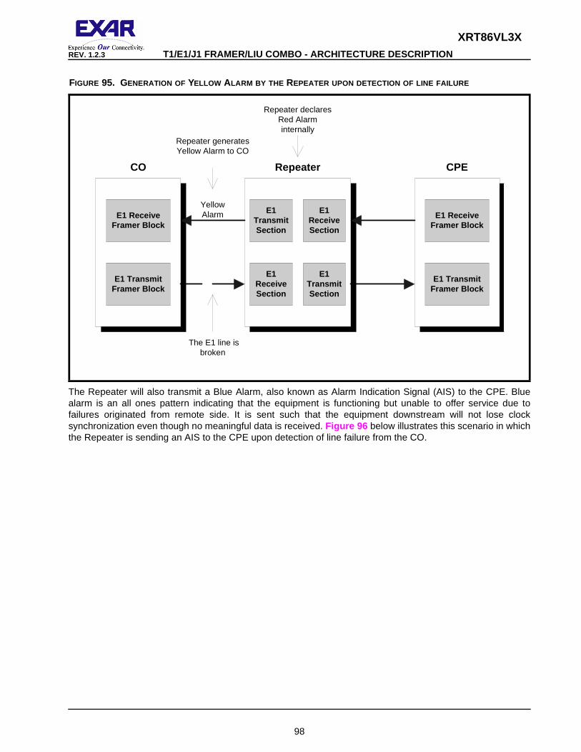
XRT86VL3X
98
REV. 1.2.3 T1/E1/J1 FRAMER/LIU COMBO - ARCHITECTURE DESCRIPTIO N
The Repeater will also transmit a Blue Alarm, also known as Alarm Indication Signal (AIS) to the CPE. Bluealarm is an all ones pattern indicating that the equipment is functioning but unable to offer service due tofailures originated from remote side. It is sent such that the equipment downstream will not lose clocksynchronization even though no meaningful data is received. Figure 96 below illustrates this scenario in whichthe Repeater is sending an AIS to the CPE upon detection of line failure from the CO.
FIGURE 95. GENERATION OF YELLOW ALARM BY THE REPEATER UPON DETECTION OF LINE FAILURE
E1 ReceiveFramer Block
E1 TransmitFramer Block
E1 ReceiveFramer Block
E1 TransmitFramer Block
E1TransmitSection
E1TransmitSection
E1ReceiveSection
E1ReceiveSection
CO Repeater CPE
The E1 line isbroken
Repeater declaresRed Alarminternally
YellowAlarm
Repeater generatesYellow Alarm to CO
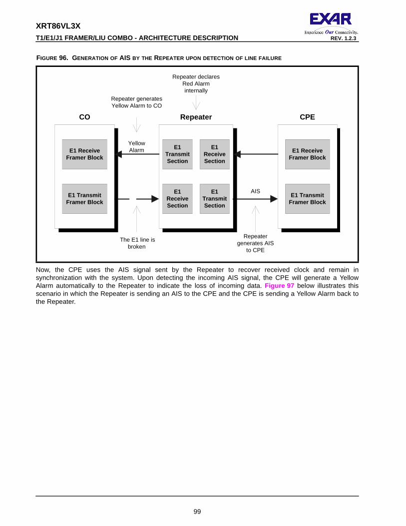
XRT86VL3X
99
T1/E1/J1 FRAMER/LIU COMBO - ARCHITECTURE DESCRIPTIO N REV. 1.2.3
Now, the CPE uses the AIS signal sent by the Repeater to recover received clock and remain insynchronization with the system. Upon detecting the incoming AIS signal, the CPE will generate a YellowAlarm automatically to the Repeater to indicate the loss of incoming data. Figure 97 below illustrates thisscenario in which the Repeater is sending an AIS to the CPE and the CPE is sending a Yellow Alarm back tothe Repeater.
FIGURE 96. GENERATION OF AIS BY THE REPEATER UPON DETECTION OF LINE FAILURE
E1 ReceiveFramer Block
E1 TransmitFramer Block
E1 ReceiveFramer Block
E1 TransmitFramer Block
E1TransmitSection
E1TransmitSection
E1ReceiveSection
E1ReceiveSection
CO Repeater CPE
The E1 line isbroken
Repeater declaresRed Alarminternally
YellowAlarm
Repeater generatesYellow Alarm to CO
Repeatergenerates AIS
to CPE
AIS
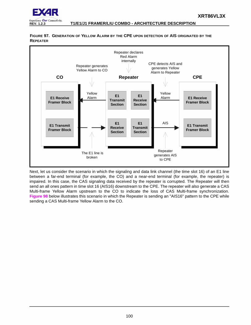
XRT86VL3X
100
REV. 1.2.3 T1/E1/J1 FRAMER/LIU COMBO - ARCHITECTURE DESCRIPTIO N
Next, let us consider the scenario in which the signaling and data link channel (the time slot 16) of an E1 linebetween a far-end terminal (for example, the CO) and a near-end terminal (for example, the repeater) isimpaired. In this case, the CAS signaling data received by the repeater is corrupted. The Repeater will thensend an all ones pattern in time slot 16 (AIS16) downstream to the CPE. The repeater will also generate a CASMulti-frame Yellow Alarm upstream to the CO to indicate the loss of CAS Multi-frame synchronization.Figure 98 below illustrates this scenario in which the Repeater is sending an "AIS16" pattern to the CPE whilesending a CAS Multi-frame Yellow Alarm to the CO.
FIGURE 97. GENERATION OF YELLOW ALARM BY THE CPE UPON DETECTION OF AIS ORIGINATED BY THE REPEATER
E1 ReceiveFramer Block
E1 TransmitFramer Block
E1 ReceiveFramer Block
E1 TransmitFramer Block
E1TransmitSection
E1TransmitSection
E1ReceiveSection
E1ReceiveSection
CO Repeater CPE
The E1 line isbroken
Repeater declaresRed Alarminternally
YellowAlarm
Repeater generatesYellow Alarm to CO
Repeatergenerates AIS
to CPE
AIS
YellowAlarm
CPE detects AIS andgenerates YellowAlarm to Repeater
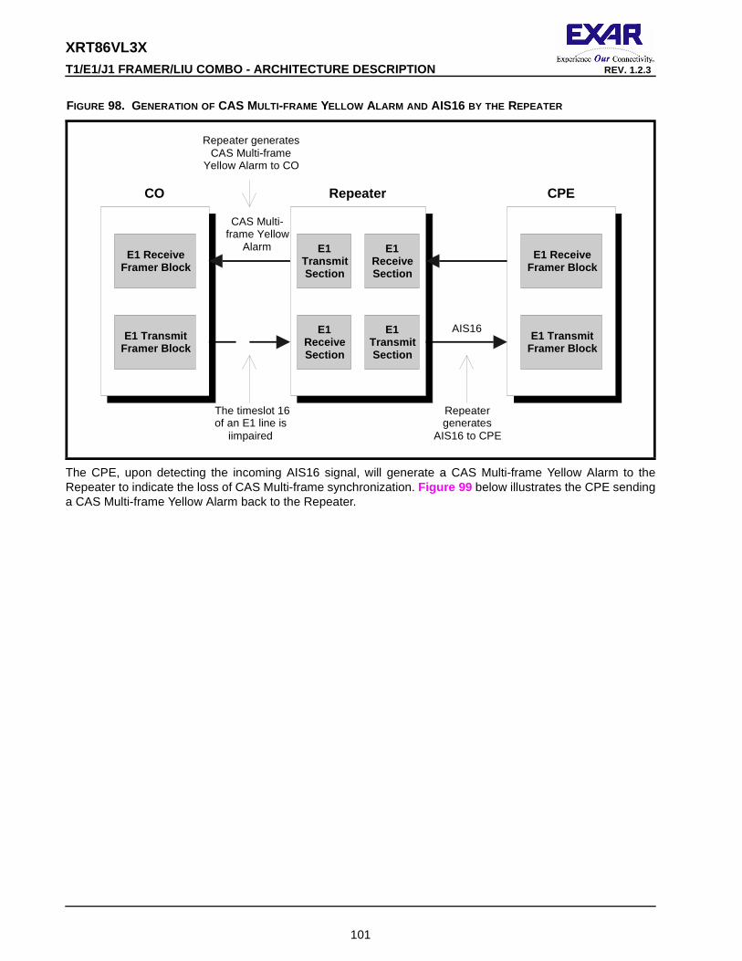
XRT86VL3X
101
T1/E1/J1 FRAMER/LIU COMBO - ARCHITECTURE DESCRIPTIO N REV. 1.2.3
The CPE, upon detecting the incoming AIS16 signal, will generate a CAS Multi-frame Yellow Alarm to theRepeater to indicate the loss of CAS Multi-frame synchronization. Figure 99 below illustrates the CPE sendinga CAS Multi-frame Yellow Alarm back to the Repeater.
FIGURE 98. GENERATION OF CAS MULTI-FRAME YELLOW ALARM AND AIS16 BY THE REPEATER
E1 Receive Framer Block
E1 Transmit Framer Block
E1 Receive Framer Block
E1 Transmit Framer Block
E1 Transmit Section
E1 Transmit Section
E1 Receive Section
E1 Receive Section
CO Repeater CPE
The timeslot 16 of an E1 line is
iimpaired
Repeater generates CAS Multi-frame
Yellow Alarm to CO
Repeater generates
AIS16 to CPE
AIS16
CAS Multi- frame Yellow
Alarm

XRT86VL3X
102
REV. 1.2.3 T1/E1/J1 FRAMER/LIU COMBO - ARCHITECTURE DESCRIPTIO N
In summary, AIS or Blue Alarm is sent by a piece of E1 equipment downstream indicating that the incomingsignal from upstream is lost. Yellow Alarm is sent by a piece of E1 equipment upstream upon detection of Lossof Signal, Loss of Frame or when it is receiving AIS.
Similarly, an "AIS16" pattern is sent by a piece of E1 equipment downstream indicating that the incoming datalink channel from upstream is damaged. The CAS Multi-frame Yellow Alarm is sent by a piece of E1 equipmentupstream upon detection of Loss of CAS Multi-frame synchronization or when it is receiving an "AIS16"pattern.
9.5.1 How to configure the framer to transmit AIS
As we discussed in the previous section, Alarm Indication Signal (AIS) or Blue Alarm is transmitted by theintermediate node to indicate that the equipment is still functioning but unable to offer services. It is an all ones(except for framing bits) pattern which can be used by the equipment further down the line to maintain clockrecovery and timing synchronization.
The XRT86VL3x framer can generate three types of AIS when it is running in E1 format:
• Framed AIS
• Unframed AIS
• AIS16
Unframed AIS is an all ones pattern. If unframed AIS is sent, the equipment further down the line will be able tomaintain timing synchronization and be able to recover clock from the received AIS signal. However, due to thelack of framing bits, the equipment farther down the line will not be able to maintain frame synchronization andwill declare Loss of Frame (LOF).
FIGURE 99. GENERATION OF CAS MULTI-FRAME YELLOW ALARM BY THE CPE UPON DETECTION OF “AIS16” PAT-TERN SENT BY THE REPEATER
E1 ReceiveFramer Block
E1 TransmitFramer Block
E1 ReceiveFramer Block
E1 TransmitFramer Block
E1TransmitSection
E1TransmitSection
E1ReceiveSection
E1ReceiveSection
CO Repeater CPE
The timeslot 16of an E1 line is
iimpaired
Repeater generatesCAS Multi-frame
Yellow Alarm to CO
Repeatergenerates
AIS16 to CPE
AIS16
CAS Multi-frame Yellow
Alarm
CPE detects AIS16and generates CASMulti-frame YellowAlarm to Repeater
CAS Multi-frame Yellow
Alarm

XRT86VL3X
103
T1/E1/J1 FRAMER/LIU COMBO - ARCHITECTURE DESCRIPTIO N REV. 1.2.3
On the other hand, the payload portion of a framed AIS pattern is all ones. However, a framed AIS pattern stillhas correct framing bits. Therefore, the equipment further down the line can still maintain framesynchronization as well as timing synchronization. In this case, no LOF or Red alarm will be declared.
"AIS16" is an AIS alarm that is supported only in E1 framing format. It is an all ones pattern in time slot 16 ofeach E1 frame. As we mentioned before, time slot 16 is usually used for signaling and data link in E1,therefore, an "AIS16" alarm is transmitted by the intermediate node to indicate that the data link channel ishaving a problem. Since all the other thirty one time slots are still transmitting normal data (that is, framinginformation and PCM data), the equipment further down the line can still maintain frame synchronization,timing synchronization as well as receive PCM data. In this case, no LOF or Red alarm will be declared by theequipment further down the line. However, a CAS Multi-frame Yellow Alarm will be sent by the equipmentfurther down the line to indicate the loss of CAS Multi-frame alignment.
The Transmit Alarm Indication Signal Select bits of the Alarm Generation Register (AGR) enable the threetypes of AIS transmission that are supported by the XRT86VL3x framer. The table below shows configurationsof the Transmit Alarm Indication Signal Select bits of the Alarm Generation Register (AGR).
9.5.2 How to configure the framer to generate Red Al arm
Upon detection of Loss of Signal (LOS) or Loss of Frame (LOF) condition, the Repeater will generate aninternal Red Alarm when enabled. This alarm will normally trigger a microprocessor interrupt informing the userthat an incoming signal failure is happening.
The Loss of Frame Declaration Enable bit of the Alarm Generation Register (AGR) enable the generation ofRed Alarm. The table below shows configurations of the of Frame Declaration Enable bit of the AlarmGeneration Register (AGR).
9.5.3 How to configure the framer to transmit Yellow Alarm
The XRT86VL3x framer supports transmission of both Yellow Alarm and CAS Multi-frame Yellow Alarm in E1mode.
ALARM GENERATION REGISTER (AGR) (ADDRESS = 0XN108H )
BIT NUMBER
BIT NAME BIT TYPE BIT DESCRIPTION
3-2 Transmit AIS Select
R/W These READ/WRITE bit-fields allows the user to choose which one of the three AIS pattern supported by the XRT86VL3x framer will be transmitted.
00 - No AIS alarm is generated.
01 - Enable unframed AIS alarm of all ones pattern.
11 - AIS16 pattern is generated. Only time slot 16 is carrying the all ones pattern. The other time slots still carry framing and PCM data.
11 - Enable framed AIS alarm of all ones pattern except for framing bits.
ALARM GENERATION REGISTER (AGR) (ADDRESS = 0XN108H )
BIT NUMBER
BIT NAME BIT TYPE BIT DESCRIPTION
6 Loss of Frame Declaration Enable
R/W This READ/WRITE bit-field permits the framer to declare Red Alarm in case of Loss of Frame Alignment (LOF).
When receiver module of the framer detects Loss of Frame Alignment in the incoming data stream, it will generate a Red Alarm. The framer will also generate an RxLOFs interrupt to notify the microprocessor that an LOF condition is occurred. A Yellow Alarm is then returned to the remote transmitter to report that the local receiver detects LOF.
0 - Red Alarm declaration is disabled.
1 - Red Alarm declaration is enabled.

XRT86VL3X
104
REV. 1.2.3 T1/E1/J1 FRAMER/LIU COMBO - ARCHITECTURE DESCRIPTIO N
Upon detection of Loss of Signal (LOS) or Loss of Frame (LOF) condition, the receiver will transmit the YellowAlarm back to the source indicating the loss of an incoming signal. This Yellow Alarm informs the source thatthere is a problem further down the line and its transmission is not being received at the destination.
On the other hand, upon detection of Loss of CAS Multi-frame alignment pattern, the receiver section of theXRT86VL3x framer will transmit a CAS Multi-frame Yellow Alarm back to the source indicating the Loss of CASMulti-frame synchronization.
The Yellow Alarm Generation Select bits of the Alarm Generation Register (AGR) enable transmission ofdifferent types of Yellow alarm that are supported by the XRT86VL3x framer.
9.5.4 Transmit Yellow Alarm
The Yellow Alarm bits are located at bit 2 of time slot 0 of non-FAS frames. A logic one of this bit denotes theYellow Alarm and a logic zero of this bit denotes normal operation. The XRT86VL3x supports transmission ofYellow Alarm automatically or manually.
When the Yellow Alarm Generation Select bits of the Alarm Generation Register are set to 01, the Yellow Alarmbit is transmitted by echoing the received FAS alignment pattern. If the correct FAS alignment is received, theYellow Alarm bit is set to zero. If the FAS alignment pattern is missing or corrupted, the Yellow Alarm bit is setto one while Loss of Frame Synchronization is declared.
When the Yellow Alarm Generation Select bits of the Alarm Generation Register are set to 10, the Yellow Alarmbit is transmitted as zero.
When the Yellow Alarm Generation Select bits of the Alarm Generation Register are set to 11, the Yellow Alarmbit is transmitted as one.
9.5.5 Transmit CAS Multi-frame Yellow Alarm
Within the sixteen-frame CAS Multi-frame, the CAS Multi-frame Yellow Alarm bits are located at bit 6 of timeslot 16 of frame number 0. A logic one of this bit denotes the CAS Multi-frame Yellow Alarm and a logic zero ofthis bit denotes normal operation. The XRT86VL3x supports transmission of CAS Multi-frame Yellow Alarmautomatically or manually.
When the CAS Multi-frame Yellow Alarm Generation Select bits of the Alarm Generation Register are set to 01,the CAS Multi-frame Yellow Alarm bit is transmitted by echoing the received CAS Multi-frame alignment pattern(the four zeros pattern). If the correct CAS Multi-frame alignment is received, the CAS Multi-frame YellowAlarm bit is set to zero. If the CAS Multi-frame alignment pattern is missing or corrupted, the CAS Multi-frameYellow Alarm bit is set to one while Loss of CAS Multi-frame Synchronization is declared.
When the CAS Multi-frame Yellow Alarm Generation Select bits of the Alarm Generation Register are set to 10,the CAS Multi-frame Yellow Alarm bit is transmitted as zero.
When the CAS Multi-frame Yellow Alarm Generation Select bits of the Alarm Generation Register are set to 11,the CAS Multi-frame Yellow Alarm bit is transmitted as one.

XRT86VL3X
105
T1/E1/J1 FRAMER/LIU COMBO - ARCHITECTURE DESCRIPTIO N REV. 1.2.3
9.6 T1 Brief discussion of alarms and error conditio ns
As defined in ANSI T1.231 specification, alarm conditions are created from defects. Defects are momentaryimpairments present on the DS1 trunk. If a defect is present for a sufficient amount of time (called theintegration time), then the defect becomes an alarm. Once an alarm is declared, the alarm is present until afterthe defect clears for a specified period of time. The time it takes to clear an alarm is called the de-integrationtime.
Alarms are used to detect and warn maintenance personnel of problems on the DS1 trunk. There are threetypes of alarms:
• Red alarm or Service Alarm Indication (SAI) Signal
• Blue alarm or Alarm Indication Signal (AIS)
• Yellow alarm or Remote Alarm Indication (RAI) Signal
A simple DS1 system model is shown in Figure 100 to explain the error conditions and generation of differentalarms, let us create. In this model, a DS1 signal is sourced from the Central Office (CO) through a Repeater tothe Customer Premises Equipment (CPE). At the same time, a DS1 signal is routed from the CPE to theRepeater and back to the Central Office.
When the DS1 system runs normally, i.e., when there is no Loss of Signal (LOS) or Loss of Frame (LOF)detected in the line, no alarm will be generated. Sometimes, intermittent outburst of electrical noises on the linemight result in Bipolar Violation or bit errors in the incoming signals, but these errors in general will not triggerthe equipment to generate alarms. They will at most trigger the framer to generate interrupts which wouldcause the local microprocessor to interrupt as well as add statistics in the performance monitoring accumulatorregisters.
Now, consider a case in which the DS1 line from the Repeater to CPE is broken or interrupted, resulting in acomplete loss of incoming data or a severely impaired signal quality. Upon detection of Loss of Signal (LOS) orLoss of Frame (LOF) condition, the CPE will generate an internal Red Alarm, also known as the Service AlarmIndication. This alarm will normally trigger a microprocessor interrupt informing the user that an incoming signalfailure is happening.
When the CPE is in the Red Alarm state, it will transmit the Yellow Alarm to the Repeater indicating the loss ofan incoming signal or loss of frame synchronization. This Yellow Alarm informs the Repeater that there is a
FIGURE 100. SIMPLE DIAGRAM OF DS1 SYSTEM MODEL
DS1 ReceiveFramer Block
DS1 TransmitFramer Block
DS1 ReceiveFramer Block
DS1 TransmitFramer Block
DS1TransmitSection
DS1TransmitSection
DS1ReceiveSection
DS1ReceiveSection
CO Repeater CPE
Simple DS1 System Model
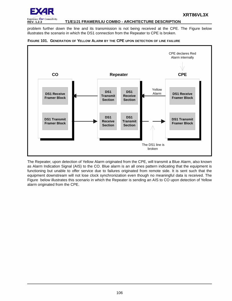
XRT86VL3X
106
REV. 1.2.3 T1/E1/J1 FRAMER/LIU COMBO - ARCHITECTURE DESCRIPTIO N
problem further down the line and its transmission is not being received at the CPE. The Figure belowillustrates the scenario in which the DS1 connection from the Repeater to CPE is broken.
The Repeater, upon detection of Yellow Alarm originated from the CPE, will transmit a Blue Alarm, also knownas Alarm Indication Signal (AIS) to the CO. Blue alarm is an all ones pattern indicating that the equipment isfunctioning but unable to offer service due to failures originated from remote side. It is sent such that theequipment downstream will not lose clock synchronization even though no meaningful data is received. TheFigure below illustrates this scenario in which the Repeater is sending an AIS to CO upon detection of Yellowalarm originated from the CPE.
FIGURE 101. GENERATION OF YELLOW ALARM BY THE CPE UPON DETECTION OF LINE FAILURE
DS1 ReceiveFramer Block
DS1 TransmitFramer Block
DS1 ReceiveFramer Block
DS1 TransmitFramer Block
DS1TransmitSection
DS1TransmitSection
DS1ReceiveSection
DS1ReceiveSection
CO Repeater CPE
The DS1 line isbroken
CPE declares RedAlarm internally
YellowAlarm

XRT86VL3X
107
T1/E1/J1 FRAMER/LIU COMBO - ARCHITECTURE DESCRIPTIO N REV. 1.2.3
Now let us consider another scenario in which the DS1 line between CO and the Repeater is broken. Again,upon detection of Loss of Signal (LOS) or Loss of Frame (LOF) condition, the Repeater will generate aninternal Red Alarm. This alarm will normally trigger a microprocessor interrupt informing the user that anincoming signal failure is happening.
The Repeater will also send an all ones AIS pattern downstream to the CPE and a Yellow Alarm back to theCO. The CPE uses the AIS signal to recover received clock and remain in synchronization with the system.Upon detecting the incoming AIS signal, the CPE will generate a Yellow Alarm to the Repeater to indicate theloss of incoming signal. The Figure below illustrates this scenario in which the Repeater is sending an AIS tothe CPE and the CPE is sending a Yellow Alarm back to the Repeater.
Generation of AIS by the Repeater upon detection of Yellow Alarm originated by the CPE
DS1 ReceiveFramer Block
DS1 TransmitFramer Block
DS1 ReceiveFramer Block
DS1 TransmitFramer Block
DS1TransmitSection
DS1TransmitSection
DS1ReceiveSection
DS1ReceiveSection
CO Repeater CPE
The DS1 line isbroken
CPE declares RedAlarm internally
YellowAlarm
Repeater detectsYellow alarm and
generate AIS to CO
AIS

XRT86VL3X
108
REV. 1.2.3 T1/E1/J1 FRAMER/LIU COMBO - ARCHITECTURE DESCRIPTIO N
9.6.1 How to configure the framer to transmit AIS
As we discussed in the previous section, Alarm Indication Signal (AIS) or Blue Alarm is transmitted by theintermediate node to indicate that the equipment is still functioning but unable to offer services. It is an all ones(except for framing bits) pattern which can be used by the equipment further down the line to maintain clockrecovery and timing synchronization.
The XRT86VL3x framer can generate two types of AIS:
• Framed AIS
• Unframed AIS
Unframed AIS is an all ones pattern. If unframed AIS is sent, the equipment further down the line will be able tomaintain timing synchronization and be able to recover clock from the received AIS signal. However, due to thelack of framing bits, the equipment farther down the line will not be able to maintain frame synchronization andwill declare Loss of Frame (LOF).
On the other hand, the payload portion of a framed AIS pattern is all ones. However, a framed AIS pattern stillhas correct framing bits. Therefore, the equipment further down the line can still maintain framesynchronization as well as timing synchronization. In this case, no LOF or Red alarm will be declared.
The Transmit Alarm Indication Signal Select bits of the Alarm Generation Register (AGR) enable the two typesof AIS transmission that are supported by the XRT86VL3x framer. The table below shows configurations of theTransmit Alarm Indication Signal Select bits of the Alarm Generation Register (AGR)
FIGURE 102. GENERATION OF YELLOW ALARM BY THE CPE UPON DETECTION OF AIS ORIGINATED BY THE REPEATER
DS1 ReceiveFramer Block
DS1 TransmitFramer Block
DS1 ReceiveFramer Block
DS1 TransmitFramer Block
DS1TransmitSection
DS1TransmitSection
DS1ReceiveSection
DS1ReceiveSection
CO Repeater CPE
The DS1 line isbroken
Repeater declaresRed Alarminternally
YellowAlarm
Repeater detectsYellow alarm and
generate AIS to CO
AIS

XRT86VL3X
109
T1/E1/J1 FRAMER/LIU COMBO - ARCHITECTURE DESCRIPTIO N REV. 1.2.3
9.6.2 How to configure the framer to generate Red Al arm
Upon detection of Loss of Signal (LOS) or Loss of Frame (LOF) condition, the Repeater will generate aninternal Red Alarm when enabled. This alarm will normally trigger a microprocessor interrupt informing the userthat an incoming signal failure is happening.
The Loss of Frame Declaration Enable bit of the Alarm Generation Register (AGR) enables the generation ofRed Alarm. The table below shows configurations of the of Frame Declaration Enable bit of the AlarmGeneration Register (AGR).
9.6.3 How to configure the framer to transmit Yellow Alarm
Upon detection of Loss of Signal (LOS) or Loss of Frame (LOF) condition, the receiver will transmit the YellowAlarm back to the source indicating the loss of an incoming signal. This Yellow Alarm informs the source thatthere is a problem further down the line and its transmission is not being received at the destination.
The XRT86VL3x framer supports transmission of Yellow Alarm when running at the following framing formats:
• SF Mode
• ESF Mode
• N Mode
• T1DM Mode
Yellow alarm is transmitted in different forms for various framing formats. The Yellow Alarm Generation Selectbits of the Alarm Generation Register (AGR) enable transmission of different types of Yellow alarm that aresupported by the XRT86VL3x framer.
ALARM GENERATION REGISTER (AGR)(ADDRESS = 0XN108H)
BIT NUMBER
BIT NAME BIT TYPE BIT DESCRIPTION
3-2 Transmit AIS Select
R/W These READ/WRITE bit-fields allows the user to choose which one of the two AIS pattern supported by the XRT86VL3x framer will be transmitted.
00 - No AIS alarm is generated.
01 - Enable unframed AIS alarm of all ones pattern.
10 - Enable framed AIS alarm of all ones pattern except for framing bits.
11 - No AIS alarm is generated.
ALARM GENERATION REGISTER (AGR)(ADDRESS = 0XN108H)
BIT NUMBER
BIT NAME BIT TYPE BIT DESCRIPTION
6 Loss of Frame Declaration Enable
R/W This READ/WRITE bit-field permits the framer to declare Red Alarm in case of Loss of Frame Alignment (LOF).
When receiver module of the framer detects Loss of Frame Alignment in the incoming data stream, it will generate a Red Alarm. The framer will also generate an RxLOFs interrupt to notify the microprocessor that an LOF condition is occurred. A Yellow Alarm is then returned to the remote transmitter to report that the local receiver detects LOF.
0 - Red Alarm declaration is disabled.
1 - Red Alarm declaration is enabled.

XRT86VL3X
110
REV. 1.2.3 T1/E1/J1 FRAMER/LIU COMBO - ARCHITECTURE DESCRIPTIO N
9.6.4 Transmit Yellow Alarm in SF Mode
In SF mode, the XRT86VL3x supports transmission of Yellow Alarm in two ways. When the Yellow AlarmGeneration Select bits of the Alarm Generation Register are set to 01 or 11, the second MSB of all DS0channels is transmitted as zero. This is Yellow Alarm for DS1 standard.
When the Yellow Alarm Generation Select bits of the Alarm Generation Register are set to 10, the Framing bitof Frame 12 is transmitted as one. This is Yellow Alarm for J1 standard.
9.6.5 Transmit Yellow Alarm in ESF Mode
In ESF mode, the XRT86VL3x transmits Yellow Alarm on the 4Kbit/s data link channel. The Facility Data Linkbits are sent in the pattern of eight ones followed by eight zeros. The number of repetitions of this patterndepends on the duration of Yellow Alarm Generation Select bits of the Alarm Generation Register. When theseselect bits are set to 01 or 11, the following scenario will happen:
1. If Bit 0 of Yellow Alarm Generation Select forms a pulse width shorter or equal to the time required to trans-mit 255 patterns on the 4Kbit/s data link, the alarm is transmitted for 255 patterns.
2. If Bit 0 of Yellow Alarm Generation Select forms a pulse width longer than the time required to transmit 255 patterns on the 4Kbit/s data link, the alarm continues until Bit 0 goes LOW.
3. A second pulse on Bit 0 of Yellow Alarm Generation Select during an alarm transmission resets the pattern counter. The framer will send another 255 patterns of the Yellow Alarm.
NOTE: To pulse Bit 0, this bit must be programmed to “1” and then reset back to “0”. The pulse width is the duration in timethat this bit remains at “1”.
When these select bits are set to 10, Bit 1 of the Yellow Alarm Generation Select forms a pulse that controls theduration of Yellow Alarm transmission. The alarm continues until Bit 1 goes LOW.
When these select bits are set to 01, the following scenario will happen:
1. If Bit 0 of Yellow Alarm Generation Select forms a pulse width shorter or equal to the time required to trans-mit 255 patterns on the 4Kbit/s data link, the alarm is transmitted for 255 patterns.
2. If Bit 0 of Yellow Alarm Generation Select forms a pulse width longer than the time required to transmit 255 patterns on the 4Kbit/s data link, the alarm continues until Bit 0 goes LOW.
3. A second pulse on Bit 0 of Yellow Alarm Generation Select during an alarm transmission resets the pattern counter. The framer will send another 255 patterns of the Yellow Alarm.
9.6.6 Transmit Yellow Alarm in N Mode
In N mode, when the Yellow Alarm Generation Select bits of the Alarm Generation Register are set to 01, 10 or11, the second MSB of all DS0 channels is transmitted as zero.
9.6.7 Transmit Yellow Alarm in T1DM Mode
In T1DM mode, when the Yellow Alarm Generation Select bits of the Alarm Generation Register are set to 01,10 or 11, the Yellow Alarm bit (the third LSB of Timeslot 23) is set to zero.The table below shows configurationsof the Yellow Alarm Generation Select bits of the Alarm Generation Register (AGR).

XRT86VL3X
111
T1/E1/J1 FRAMER/LIU COMBO - ARCHITECTURE DESCRIPTIO N REV. 1.2.3
)
ALARM GENERATION REGISTER (AGR)(ADDRESS = 0XN108H)
BIT NUMBER
BIT NAME BIT TYPE BIT DESCRIPTION
5-4 Yellow Alarm
Generation Select
R/W 00 - Transmission of Yellow Alarm is disabled.
01 - The framer transmits Yellow Alarm by converting the second MSB of all outgoing twenty-four DS0 channel into zero.
10 - The framer transmits Yellow Alarm by sending the Super-frame Align-ment Bit (Fs) of Frame 12 as one.
11 - The framer transmits Yellow Alarm by converting the second MSB of all outgoing twenty-four DS0 channel into zero.
N Mode:
00 - Transmission of Yellow Alarm is disabled.
01, 10 or 11 - The framer transmits Yellow Alarm by converting the second MSB of all outgoing twenty-four DS0 channel into zero.
ESF Mode:
When the framer is in ESF mode, it transmits Yellow Alarm pattern of eight ones followed by eight zeros (1111_1111_0000_0000) through the 4Kbit/s data link bits.
00 - Transmission of Yellow Alarm is disabled.
01 - The following scenario will happen:
1. If Bit 0 of Yellow Alarm Generation Select forms a pulse width shorter or equal to the time required to transmit 255 patterns on the 4Kbit/s data link, the alarm is transmitted for 255 patterns.
2. If Bit 0 of Yellow Alarm Generation Select forms a pulse width longer than the time required to transmit 255 patterns on the 4Kbit/s data link, the alarm continues until Bit 0 goes LOW.
3. A second pulse on Bit 0 of Yellow Alarm Generation Select during an alarm transmission resets the pattern counter. The framer will send another 255 patterns of the Yellow Alarm.
10 - Bit 1 of the Yellow Alarm Generation Select forms a pulse that controls the duration of Yellow Alarm transmission. The alarm continues until Bit 1 goes LOW.
11 - The following scenario will happen:
1. If Bit 0 of Yellow Alarm Generation Select forms a pulse width shorter or equal to the time required to transmit 255 patterns on the 4Kbit/s data link, the alarm is transmitted for 255 patterns.
2. If Bit 0 of Yellow Alarm Generation Select forms a pulse width longer than the time required to transmit 255 patterns on the 4Kbit/s data link, the alarm continues until Bit 0 goes LOW.
3. A second pulse on Bit 0 of Yellow Alarm Generation Select during an alarm transmission resets the pattern counter. The framer will send another 255 patterns of the Yellow Alarm.
T1DM Mode:
00 - Transmission of Yellow Alarm is disabled.
01, 10 or 11 - The framer transmits Yellow Alarm by setting the Yellow Alarm bit (Y-bit) to zero.

XRT86VL3X
112
REV. 1.2.3 T1/E1/J1 FRAMER/LIU COMBO - ARCHITECTURE DESCRIPTIO N
10.0 APPENDIX A: DS-1/E1 FRAMING FORMATS
10.1 The E1 Framing Structure
A single E1 frame consists of 256 bits which is created 8000 times per second. This yields a bit-rate of2.048Mbps. The 256 bits within each E1 frame are grouped into 32 octets or timeslots. These timeslots arenumbered from 0 to 31. Each timeslot is 8 bits in length and is transmitted most significant bit first, numberedbit 0. Figure 103 presents a diagram of a single E1 frame.
Not all of these timeslots are available to transmit voice or user data. For instance, timeslot 0 is always reserved forsystem use and timeslot 16 is sometimes used (reserved) by the system. Hence, within each E1 frame, either 30or 31 of the 32 timeslots are available for transporting user or voice data. In general, there are two types of E1frames, FAS and Non-FAS. In any E1 data stream, the E1 frame begins with a FAS frame followed by Non-FAS frame and then alternates between the two.
10.1.1 FAS Frame
Timeslot 0 within the FAS E1 frame contains a framing alignment pattern and therefore supports framing. Thebit-format of timeslot 0 is presented in Table 7 . The Si bit within the FAS E1 Frame typically carries the resultsof a CRC-4 calculation. The fixed framing pattern (e.g., 0, 0, 1, 1, 0, 1, 1) will be used by the Receive E1Framer at the Remote terminal for frame synchronization/alignment purposes.
FIGURE 103. SINGLE E1 FRAME DIAGRAM
TABLE 7: B IT FORMAT OF TIMESLOT 0 OCTET WITHIN A FAS E1 FRAME
BIT 0 1 2 3 4 5 6 7
Value SI 0 0 1 1 0 1 1
Function International Bit Frame Alignment Signaling (FAS) Pattern
Description-Operation
In practice, the Si bit within the FAS E1 Frame carries the results of a CRC-4 calculation, which is discussed in greater detail in Section 10.2.1.
The fixed framing pattern (e.g., 0, 0, 1, 1, 0, 1, 1) is used by the Receive E1 Framer at the Remote terminal for frame synchronization/alignment purposes.
Timeslot 0 Timeslot 1 Timeslot 29
0 1 2 3 4 5 6 7
Timeslot 30 Timeslot 31
E1 Frame
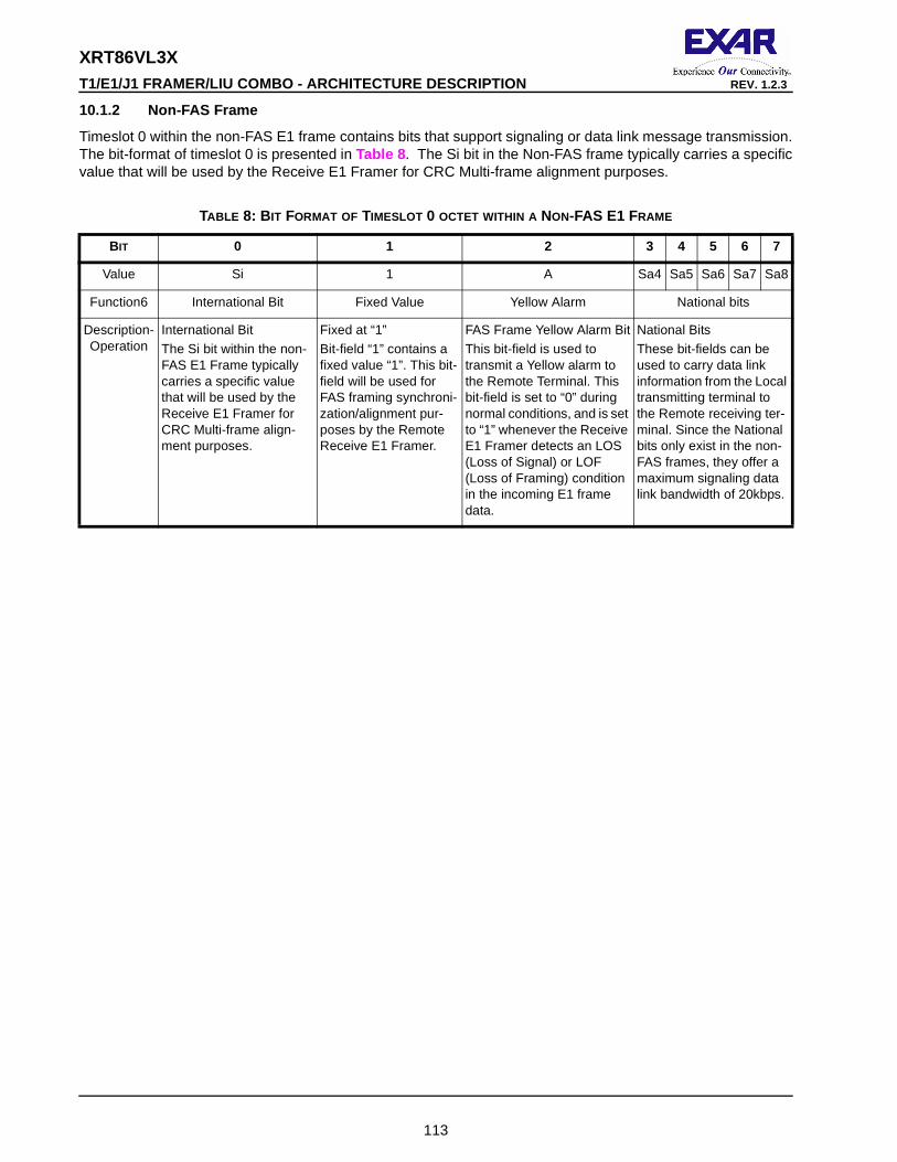
XRT86VL3X
113
T1/E1/J1 FRAMER/LIU COMBO - ARCHITECTURE DESCRIPTIO N REV. 1.2.3
10.1.2 Non-FAS Frame
Timeslot 0 within the non-FAS E1 frame contains bits that support signaling or data link message transmission.The bit-format of timeslot 0 is presented in Table 8 . The Si bit in the Non-FAS frame typically carries a specificvalue that will be used by the Receive E1 Framer for CRC Multi-frame alignment purposes.
TABLE 8: B IT FORMAT OF TIMESLOT 0 OCTET WITHIN A NON-FAS E1 FRAME
BIT 0 1 2 3 4 5 6 7
Value Si 1 A Sa4 Sa5 Sa6 Sa7 Sa8
Function6 International Bit Fixed Value Yellow Alarm National bits
Description-Operation
International Bit
The Si bit within the non-FAS E1 Frame typically carries a specific value that will be used by the Receive E1 Framer for CRC Multi-frame align-ment purposes.
Fixed at “1”
Bit-field “1” contains a fixed value “1”. This bit-field will be used for FAS framing synchroni-zation/alignment pur-poses by the Remote Receive E1 Framer.
FAS Frame Yellow Alarm Bit
This bit-field is used to transmit a Yellow alarm to the Remote Terminal. This bit-field is set to “0” during normal conditions, and is set to “1” whenever the Receive E1 Framer detects an LOS (Loss of Signal) or LOF (Loss of Framing) condition in the incoming E1 frame data.
National Bits
These bit-fields can be used to carry data link information from the Local transmitting terminal to the Remote receiving ter-minal. Since the National bits only exist in the non-FAS frames, they offer a maximum signaling data link bandwidth of 20kbps.
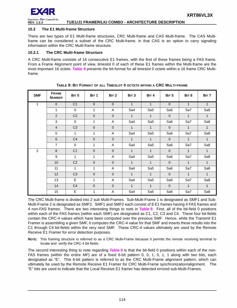
XRT86VL3X
114
REV. 1.2.3 T1/E1/J1 FRAMER/LIU COMBO - ARCHITECTURE DESCRIPTIO N
10.2 The E1 Multi-frame Structure
There are two types of E1 Multi-frame structures, CRC Multi-frame and CAS Multi-frame. The CAS Multi-frame can be considered a subset of the CRC Multi-frame, in that CAS is an option to carry signalinginformation within the CRC Multi-frame structure.
10.2.1 The CRC Multi-frame Structure
A CRC Multi-frame consists of 16 consecutive E1 frames, with the first of these frames being a FAS frame.From a Frame Alignment point of view, timeslot 0 of each of these E1 frames within the Multi-frame are themost important 16 octets. Table 9 presents the bit-format for all timeslot 0 octets within a 16 frame CRC Multi-frame.
The CRC Multi-frame is divided into 2 sub Multi-Frames. Sub-Multi-Frame 1 is designated as SMF1 and Sub-Multi-Frame 2 is designated as SMF2. SMF1 and SMF2 each consist of 8 E1 frames having 4 FAS frames and4 non-FAS frames. There are two interesting things to note in Table 9 . First, all of the bit-field 0 positionswithin each of the FAS frames (within each SMF) are designated as C1, C2, C3 and C4. These four bit-fieldscontain the CRC-4 values which have been computed over the previous SMF. Hence, while the Transmit E1Framer is assembling a given SMF, it computes the CRC-4 value for that SMF and inserts these results into theC1 through C4 bit-fields within the very next SMF. These CRC-4 values ultimately are used by the RemoteReceive E1 Framer for error detection purposes.
NOTE: This framing structure is referred to as a CRC Multi-Frame because it permits the remote receiving terminal tolocate and verify the CRC-4 bit-fields.
The second interesting thing to note regarding Table 9 is that the bit-field 0 positions within each of the non-FAS frames (within the entire MF) are of a fixed 6-bit pattern 0, 0, 1, 0, 1, 1 along with two bits, eachdesignated as “E”. This 6-bit pattern is referred to as the CRC Multi-Frame alignment pattern, which canultimately be used by the Remote Receive E1 Framer for CRC Multi-Frame synchronization/alignment. The"E" bits are used to indicate that the Local Receive E1 framer has detected errored sub-Multi-Frames.
TABLE 9: B IT FORMAT OF ALL TIMESLOT 0 OCTETS WITHIN A CRC MULTI-FRAME
SMFFRAME
NUMBERBIT 0 BIT 1 BIT 2 B IT 3 BIT 4 BIT 5 BIT 6 BIT 7
1 0 C1 0 0 1 1 0 1 1
1 0 1 A Sa4 Sa5 Sa6 Sa7 Sa8
2 C2 0 0 1 1 0 1 1
3 0 1 A Sa4 Sa5 Sa6 Sa7 Sa8
4 C3 0 0 1 1 0 1 1
5 1 1 A Sa4 Sa5 Sa6 Sa7 Sa8
6 C4 0 0 1 1 0 1 1
7 0 1 A Sa4 Sa5 Sa6 Sa7 Sa8
2 8 C1 0 0 1 1 0 1 1
9 1 1 A Sa4 Sa5 Sa6 Sa7 Sa8
10 C2 0 0 1 1 0 1 1
11 1 1 A Sa4 Sa5 Sa6 Sa7 Sa8
12 C3 0 0 1 1 0 1 1
13 E 1 A Sa4 Sa5 Sa6 Sa7 Sa8
14 C4 0 0 1 1 0 1 1
15 E 1 A Sa4 Sa5 Sa6 Sa7 Sa8

XRT86VL3X
115
T1/E1/J1 FRAMER/LIU COMBO - ARCHITECTURE DESCRIPTIO N REV. 1.2.3
10.2.2 CAS Multi-Frames and Channel Associated Signa ling
CAS Multi-Frames are only relevant if the user is using CAS or Channel Associated Signaling. If the user isimplementing Common Channel Signaling then the CAS Multi-Frame is not available.
10.2.2.1 Channel Associated Signaling
If the user operates an E1 channel in Channel Associated Signaling, then timeslot 16 octets within each E1frame will be reserved for signaling. Such signaling would convey information such as On-Hook, Off-Hookconditions, call set-up, control, etc. In CAS, this type of signaling data that is associated with a particular voicechannel will be carried within timeslot 16 of a particular E1 frame within a CAS Multi-Frame. The CAS iscarried in a Multi-Frame structure which consists of 16 consecutive E1 frames. The framing/byte format of aCAS Multi-Frame is presented in Figure 104 .
Timeslot 16 within frame 0 is a special octet that is used to convey CAS Multi-Frame alignment information,and to convey Multi-Frame alarm information to the Remote Terminal. The bit-format of timeslot 16 withinframe 0 of a CAS Multi-Frame is 0000 xyxx. The upper nibble of this octet contains all zeros and is used toidentify itself as the CAS Multi-Frame alignment signal. If CAS is used, then the user is advised to insure thatnone of the other timeslot 16 octets contain the value "0000". The lower nibble of this octet contains theexpression "xyxx". The x-bits are the spare bits and should be set to "0" if not used. The y-bit is used toindicate a Multi-Frame alarm condition to the Remote terminal. During normal operation, this bit-field iscleared to "0". However, if the Local Receive E1 Framer detects a problem with the incoming Multi-Frames,then the Local Transmit E1 Framer will set this bit-field within the next outbound CAS Multi-Frame to "1".
NOTE: The Local Transmit E1 Framer will continue to set the y-bit to "1" for the duration that the Local Receive E1 Framerdetects this problem.
Timeslot 16 within Frame 1 of the CAS Multi-Frame contains 4 bits of signaling data for voice channel 1 and 4bits of signaling data for voice channel 17. Timeslot 16 within Frame 2 contains 4 bits of signaling data forvoice channel 2 and 4 bits of signaling data for voice channel 18, and this continues for all E1 frames.
FIGURE 104. FRAME/BYTE FORMAT OF THE CAS MULTI-FRAME STRUCTURE
Frame 0 Frame 1 Frame 2 Frame 15
0000 xyxx
Timeslot 16 Timeslot 16 Timeslot 16 Timeslot 16
ABCD ABCD
Signaling Data Associated with Timeslot 1
Signaling DataAssociated with Timeslot 17
ABCD ABCD ABCD ABCD
CAS MultiframeAlignment Pattern
x = “dummy bits”y = Carries the Multiframe “Yellow Alarm” bit
Signaling DataAssociated withTimeslot 2
Signaling Data Associated withTimeslot 18
Signaling Data Associated withTimeslot 15
Signaling DataAssociated with Timeslot 31
A Single CAS Multiframe

XRT86VL3X
116
REV. 1.2.3 T1/E1/J1 FRAMER/LIU COMBO - ARCHITECTURE DESCRIPTIO N
10.2.2.2 Common Channel Signaling (CCS)
Common Channel Signaling is an alternative form of signaling from CAS. In CCS, whatever signaling datawhich is transported via the outbound E1 data stream, carries information that applies to all of the voicechannels as a set (e.g., timeslots 1 through 15 and 17 through 31) in the E1 frame. There are numerous othervariations of Common Channel Signaling that are available. Some of these are listed below.
• 31 Voice Channels with the common channel signaling being transported via the National Bits.
• 30 Voice Channels with the common channel signaling data being transported via the National Bits and CASdata being transported via timeslot 16.
• 30 Voice Channels with the Common Channel Signaling being processed via timeslot 16. (e.g., Primary RateISDN Signaling).
FIGURE 105. E1 FRAME FORMAT
FR0
FR1
FR2
FR3
FR4
FR5
FR6
FR15
FR14
FR13
FR12
FR11
FR10
FR9
FR8
FR7
1 NNNNNA1 A DCBADCB 0 7654321
1 1101100 0 XXYX000
TS0
TS1
TS2
TS15
TS31
TS30
TS29
TS18 - 28
TS17
TS16
TS3 - 14
FAS CAS
Time Slot 16Time Slot 0 Time Slots 1-15, 17-31
Channel Data
b. Frames 1-15b. Odd Frames 1, 3, 5-15
a. Even Frames 0, 2, 4-14 a. Frame 0
8 Bits/Time Slot
32 Time Slots/Frame
16 Frames/Multiframe
Non-FAS

XRT86VL3X
117
T1/E1/J1 FRAMER/LIU COMBO - ARCHITECTURE DESCRIPTIO N REV. 1.2.3
10.3 The DS1 Framing Structure
A single T1 frame is 193 bits long and is transmitted at a frame rate of 8000Hz. This results in an aggregate bitrate of 1.544 Mbit/s. Basic frames are divided into 24 timeslots numbered 1 thru 24 and a framing bit as shownin Figure 106 . Each timeslot is 8 bits in length and is transmitted most significant bit first, numbered bit 0. Thisresults in a single timeslot data rate of 8 bits x 8000/sec = 64 kbit/s.
FIGURE 106. T1 FRAME FORMAT
DS1 Frame
Bit0
0 Bit1
1 Bit2
2 Bit3
3 Bit4
4 Bit5
5 Bit6
6 Bit7
7
F-bitTimeslot
1Timeslot
2 - 23Timeslot
24Timeslot
23
125µµµµs

XRT86VL3X
118
REV. 1.2.3 T1/E1/J1 FRAMER/LIU COMBO - ARCHITECTURE DESCRIPTIO N
10.4 T1 Super Frame Format (SF)
The Superframe Format (SF), is also referred to as the D4 format. The requirement for associated signaling inframes 6 and 12 dictates that the frames be distinguishable. This leads to a multiframe structure consisting of12 frames per superframe (SF) as shown in Figure 107 and Table 10 . This structure of frames andmultiframes is defined by the F-bit pattern. The F-bit is designated alternately as an Ft bit (terminal framing bit)or Fs bit (signalling framing bit). The Ft bit carries a pattern of alternating zeros and ones (101010) in oddframes that defines the boundaries so that one timeslot may be distinguished from another. The Fs bit carriesa pattern of (001110) in even frames and defines the multiframe boundaries so that one frame may bedistinguished from another.
FIGURE 107. T1 SUPERFRAME PCM FORMAT
TABLE 10: SUPERFRAME FORMAT
FRAME BIT
F-B ITS BIT USE IN EACH TIMESLOTSIGNALLING
CHANNELTERMINAL
FRAMING FT
TERMINAL
FRAMING FSTRAFFIC SIG
1 0 1 ---- 1-8 ---- ----
2 193 ---- 0 1-8 ---- ----
3 386 0 ---- 1-8 ---- ----
4 579 ---- 0 1-8 ---- ----
5 772 1 ---- 1-8 ---- ----
6 965 ---- 1 1-7 8 A
7 1158 0 ---- 1-8 ---- ----
8 1351 ---- 1 1-8 ---- ----
B
A
Bit 0 Bit 1 Bit 2 Bit 3 Bit 4 Bit 5 Bit 6 Bit 7
8 Bits per Timeslot
FtorFs
FtorFs
TS1
TS1 TS
2
TS2 ------------------
------------------ TS13
TS13 -------------------
------------------- TS24
TS24
FR1
FR1 FR
2
FR2 ------------------
------------------ FR7
FR7 -------------------
------------------- FR11
FR11 FR
12
FR12
Signalling InformationBit 7During:Frame 12Frame 6
24 Timeslots per FrameFrame = 193 Bits
MultiframeSF = 12 Frames

XRT86VL3X
119
T1/E1/J1 FRAMER/LIU COMBO - ARCHITECTURE DESCRIPTIO N REV. 1.2.3
10.5 T1 Extended Superframe Format (ESF)
In Extended Superframe Format (ESF), as shown in Figure 108 and Table 11 , the multiframe structure isextended to 24 frames. The timeslot structure is identical to D4 (SF) format. Robbed-bit signaling isaccommodated in frame 6 (A-bit), frame 12 (B-bit), frame 18 (C-bit) and frame 24 (D-bit).
The F-bit pattern of ESF contains three functions:
1. Framing Pattern Sequence (FPS), which defines the frame and multiframe boundaries.2. Facility Data Link (FDL), which allows data such as error-performance to be passed within the T1 link.3. Cyclic Redundancy Check (CRC), which allows error performance to be monitored and enhances the reli-
ability of the receiver’s framing algorithm.
9 1544 1 ---- 1-8 ---- ----
10 1737 ---- 1 1-8 ---- ----
11 1930 0 ---- 1-8 ---- ----
12 2123 ---- 0 1-7 8 B
FIGURE 108. T1 EXTENDED SUPERFRAME FORMAT
TABLE 10: SUPERFRAME FORMAT
FRAME BIT
F-B ITS BIT USE IN EACH TIMESLOTSIGNALLING
CHANNELTERMINAL
FRAMING FT
TERMINAL
FRAMING FSTRAFFIC SIG
D
C
CRCCRC
FDL
FDL
B
A
Bit0
Bit1
Bit2
Bit3
Bit4
Bit5
Bit6
Bit7
8 Bits perTimeslot
FPSorFs
FPSorFs
TS1
TS1 TS
2
TS2 -----------------
-
------------------ TS
13
TS13 ------------------
-
------------------- TS
24
TS24
FR1
FR1 FR
2
FR2 -----------------
-
------------------ FR
13
FR13 ------------------
-
------------------- FR
23
FR23 FR
24
FR24
SignallingInformation
Bit 7During:Frame 24Frame 18Frame 12Frame 6
24 Timeslots per FrameFrame = 193 Bits
MultiframeESF = 24Frames
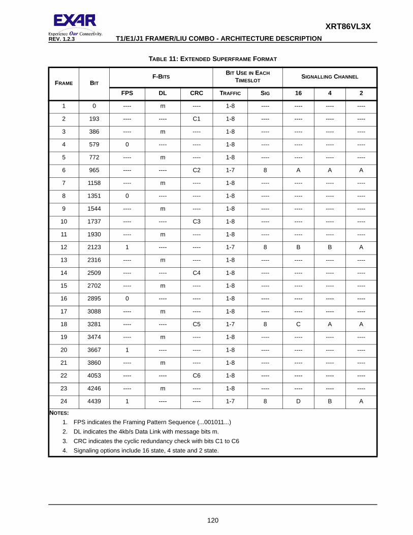
XRT86VL3X
120
REV. 1.2.3 T1/E1/J1 FRAMER/LIU COMBO - ARCHITECTURE DESCRIPTIO N
TABLE 11: EXTENDED SUPERFRAME FORMAT
FRAME BITF-BITS
BIT USE IN EACH TIMESLOT
SIGNALLING CHANNEL
FPS DL CRC TRAFFIC SIG 16 4 2
1 0 ---- m ---- 1-8 ---- ---- ---- ----
2 193 ---- ---- C1 1-8 ---- ---- ---- ----
3 386 ---- m ---- 1-8 ---- ---- ---- ----
4 579 0 ---- ---- 1-8 ---- ---- ---- ----
5 772 ---- m ---- 1-8 ---- ---- ---- ----
6 965 ---- ---- C2 1-7 8 A A A
7 1158 ---- m ---- 1-8 ---- ---- ---- ----
8 1351 0 ---- ---- 1-8 ---- ---- ---- ----
9 1544 ---- m ---- 1-8 ---- ---- ---- ----
10 1737 ---- ---- C3 1-8 ---- ---- ---- ----
11 1930 ---- m ---- 1-8 ---- ---- ---- ----
12 2123 1 ---- ---- 1-7 8 B B A
13 2316 ---- m ---- 1-8 ---- ---- ---- ----
14 2509 ---- ---- C4 1-8 ---- ---- ---- ----
15 2702 ---- m ---- 1-8 ---- ---- ---- ----
16 2895 0 ---- ---- 1-8 ---- ---- ---- ----
17 3088 ---- m ---- 1-8 ---- ---- ---- ----
18 3281 ---- ---- C5 1-7 8 C A A
19 3474 ---- m ---- 1-8 ---- ---- ---- ----
20 3667 1 ---- ---- 1-8 ---- ---- ---- ----
21 3860 ---- m ---- 1-8 ---- ---- ---- ----
22 4053 ---- ---- C6 1-8 ---- ---- ---- ----
23 4246 ---- m ---- 1-8 ---- ---- ---- ----
24 4439 1 ---- ---- 1-7 8 D B A
NOTES:
1. FPS indicates the Framing Pattern Sequence (...001011...)
2. DL indicates the 4kb/s Data Link with message bits m.
3. CRC indicates the cyclic redundancy check with bits C1 to C6
4. Signaling options include 16 state, 4 state and 2 state.

XRT86VL3X
121
T1/E1/J1 FRAMER/LIU COMBO - ARCHITECTURE DESCRIPTIO N REV. 1.2.3
10.6 T1 Non-Signaling Frame Format
The Non-Signaling (N) framing format is a simplified version of the T1 super frame. The N-Frame consists offour frames with two Fs bits and two Ft bits. The Fs bits can be used as a proprietary 4kbps data linktransmission. Signaling is not supported in this framing format.
10.7 T1 Data Multiplexed Framing Format (T1DM)
T1DM uses a similar framing structure as the SF (D4), such that the Fs and Ft bits on the individual frameboundaries remain the same. The differentiation between T1DM and SF is within the payload time slots. Timeslot 24 cannot be used for data when configured for T1DM. Time slot 24 is dedicated for a specialsynchronization byte as shown in Figure 109 . The Y-bit is to carry the status of the Yellow Alarm. The R-bit isdedicated for a remote signaling bit typically not used. However, the framer allows this bit to carry an HDLCmessage. Time slots 1 through 23 are used to carry the seven bit word from each of the 23 DS-0 signals.
TABLE 12: NON-SIGNALING FRAMING FORMAT
FRAME BIT
F-B ITS
TERMINAL
FRAMING FT
TERMINAL
FRAMING FS
1 0 1 ----
2 193 ---- X
3 386 0 ----
4 579 ---- X
FIGURE 109. T1DM FRAME FORMAT
FTime Slot
1Time Slots
2 through 23Time Slot
24
Bit 1 Bit 2 Bit 3 Bit 4 Bit 6 Bit 7 CBit 5 1 0 1 1 Y R 01
12 T1DM Framesper Multi-frameT1DM Frame

XRT86VL3X
122
REV. 1.2.3 T1/E1/J1 FRAMER/LIU COMBO - ARCHITECTURE DESCRIPTIO N
10.8 SLC-96 Format (SLC-96)
SLC framing mode allows synchronization to the SLC®96 data link pattern. This pattern described in BellcoreTR-TSY-000008, contains both signaling information and a framing pattern that overwrites the Fs bit of the SFframer pattern. See Table 13 .
TABLE 13: SLC®96 FS BIT CONTENTS
FRAME # FS BIT FRAME # FS BIT FRAME # FS BIT
2 0 26 C2 50 0
4 0 28 C3 52 M1
6 1 30 C4 54 M2
8 1 32 C5 56 M3
10 1 34 C6 58 A1
12 0 36 C7 60 A2
14 0 38 C8 62 S1
16 0 40 C9 64 S2
18 1 42 C10 66 S3
20 1 44 C11 68 S4
22 1 46 0 70 1
24 C1 48 1 72 0
NOTES:
1. The SLC®96 frame format is similar to that of SF as shown in Table 10 with the exceptionsshown in this table.
2. C1 to C11 are concentrator bit fields.
3. M1 to M3 are Maintenance bit fields.
4. A1 and A2 are alarm bit fields.
5. S1 to S4 are line switch bit fields.
6. The Fs bits in frames 46, 48 and 70 are spoiler bit switch are used to protect against falsemultiframing.

XRT86VL3X
123
T1/E1/J1 FRAMER/LIU COMBO - ARCHITECTURE DESCRIPTIO N REV. 1.2.3
ELECTRICAL CHARACTERISTICS
ABSOLUTE MAXIMUMS
Power Supply.....................................................................
VDDIO .. ................................................ -0.5V to +3.465V
VDDCORE...............................................-0.5V to +1.890V
Power Rating PBGA Package..................................1.39W
(XRT86VL32/VL34)
Power Rating STBGA and PBGA Package ...............2.4W
(XRT86VL38)
Storage Temperature ...............................-65°C to 150°C Input Logic Signal Voltage (Any Pin) .........-0.5V to + 5.5V
Operating Temperature Range.................-40°C t o 85°C ESD Protection (HBM)......................... ..................>2000V
Supply Voltage ...................... GND-0.5V to +VDD + 0.5V Input Current (Any Pin) ...................................... + 100mA
DC ELECTRICAL CHARACTERISTICS
Test Conditions: TA = 25°C, VDD IO = 3.3V + 5% , VDDCORE = 1.8V + 5% unless otherwise specified
SYMBOL PARAMETER MIN. TYP. MAX. UNITS CONDITIONS
ILL Data Bus Tri-State Bus Leakage Current -10 +10 µA
VIL Input Low voltage 0.8 V
VIH Input High Voltage 2.0 VDD V
VOL Output Low Voltage 0.0 0.4 V IOL = -1.6mA
VOH Output High Voltage 2.4 VDD V IOH = 40µA
IOC Open Drain Output Leakage Current µA
IIH Input High Voltage Current -10 10 µA VIH = VDD
IIL Input Low Voltage Current -10 10 µA VIL = GND
TABLE 14: XRT86VL32 POWER CONSUMPTION
VDDIO = 3.3V + 5% , VDDCORE = 1.8V + 5% , TA=25°C, UNLESS OTHERWISE SPECIFIED
MODESUPPLY
VOLTAGEIMPEDANCE
TERMINATION
RESISTOR
TRANSFORMER RATIOTYP. MAX. UNIT
TEST
CONDITIONSRECEIVER TRANSMITTER
E1 3.3V 75Ω Internal 1:1 1:2 776 mW PRBS Pattern
E1 3.3V 120Ω Internal 1:1 1:2 724 mW PRBS Pattern
T1 3.3V 100Ω Internal 1:1 1:2 829 mW PRBS Pattern

XRT86VL3X
124
REV. 1.2.3 T1/E1/J1 FRAMER/LIU COMBO - ARCHITECTURE DESCRIPTIO N
TABLE 15: XRT86VL34 POWER CONSUMPTION
VDDIO = 3.3V + 5% , VDDCORE = 1.8V + 5% , TA=25°C, UNLESS OTHERWISE SPECIFIED
MODESUPPLY
VOLTAGEIMPEDANCE
TERMINATION
RESISTOR
TRANSFORMER RATIOTYP. MAX. UNIT
TEST
CONDITIONSRECEIVER TRANSMITTER
E1 3.3V 75Ω Internal 1:1 1:2 1.035 W PRBS Pattern
E1 3.3V 120Ω Internal 1:1 1:2 0.965 W PRBS Pattern
T1 3.3V 100Ω Internal 1:1 1:2 1.105 W PRBS Pattern
TABLE 16: XRT86VL38 POWER CONSUMPTION
VDDIO = 3.3V + 5% , VDDCORE = 1.8V + 5% , TA=25°C, UNLESS OTHERWISE SPECIFIED
MODESUPPLY
VOLTAGEIMPEDANCE
TERMINATION
RESISTOR
TRANSFORMER RATIOTYP. MAX. UNIT
TEST
CONDITIONSRECEIVER TRANSMITTER
E1 3.3V 75Ω Internal 1:1 1:2 2.070 W PRBS Pattern
E1 3.3V 120Ω Internal 1:1 1:2 1.930 W PRBS Pattern
T1 3.3V 100Ω Internal 1:1 1:2 2.210 W PRBS Pattern

XRT86VL3X
125
T1/E1/J1 FRAMER/LIU COMBO - ARCHITECTURE DESCRIPTIO N REV. 1.2.3
AC ELECTRICAL CHARACTERISTICS TRANSMIT FRAMER (BASE RATE/NON-MUX)
Test Conditions: TA = 25°C, VDD = 3.3V + 5% unless otherwise specified
SYMBOL PARAMETER MIN. TYP. MAX. UNITS CONDITIONS
t1 TxSERCLK to TxMSYNC delay 234 nS
t2 TxSERCLK to TxSYNC delay 230 nS
t3 TxSERCLK to TxSER data delay 230 nS
t4 Rising Edge of TxSERCLK to Rising Edge of TxCH-CLK
13 nS
t5 Rising Edge of TxCHCLK to Valid TxCHN[4:0] Data 6 nS
t6 TxSERCLK to TxSIG delay 230 nS
t7 TxSERCLK to TxFRACT delay 110 nS
FIGURE 110. FRAMER SYSTEM TRANSMIT TIMING DIAGRAM (BASE RATE/NON-MUX)
TxMSYNC
TxSERCLK
TxSER
TxSYNC
TxCHN[4:0](Output)
TxCHCLK(Output)
TxCHN_0(TxSIG)
TxCHN_1(TxFRACT)
t1
t3
t5
t2
t4
t6
t7
A B C D

XRT86VL3X
126
REV. 1.2.3 T1/E1/J1 FRAMER/LIU COMBO - ARCHITECTURE DESCRIPTIO N
AC ELECTRICAL CHARACTERISTICS RECEIVE FRAMER (BASE RATE/NON-MUX)
Test Conditions: TA = 25°C, VDD = 3.3V + 5% unless otherwise specified
SYMBOL PARAMETER MIN. TYP. MAX. UNITS CONDITIONS
RxSERCLK as an Output
t8 Rising Edge of RxSERCLK to Rising Edge of RxCASYNC
4 nS
t9 Rising Edge of RxSERCLK to Rising Edge of RxCRCSYNC
4 nS
t10 Rising Edge of RxSERCLK to Rising Edge of RxSYNC (RxSYNC as Output)
4 nS
t11 Rising Edge of RxSERCLK to Rising Edge of RxSER
6 nS
t12 Rising Edge of RxSERCLK to Rising Edge of Valid RxCHN[4:0] data
6 nS
RxSERCLK as an Input
t13 Rising Edge of RxSERCLK to Rising Edge of RxCASYNC
8 nS
t14 Rising Edge of RxSERCLK to Rising Edge of RxCRCSYNC
8 nS
t15 Rising Edge of RxSERCLK to Rising Edge of RxSYNC (RxSYNC as Output)
10 nS
t15 Rising Edge of RxSERCLK to Rising Edge of RxSYNC (RxSYNC as Input)
230 nS
t16 Rising Edge of RxSERCLK to Rising Edge of RxSER
10 nS
t17 Rising Edge of RxSERCLK to Rising Edge of Valid RxCHN[4:0] data
9 nS
FIGURE 111. FRAMER SYSTEM RECEIVE TIMING DIAGRAM (RXSERCLK AS AN OUTPUT)
RxCRCSYNC
RxCASYNC
RxSERCLK(Output)
RxSER
RxSYNC
RxCHN[4:0]
t8
t9
t10
t11
t12

XRT86VL3X
127
T1/E1/J1 FRAMER/LIU COMBO - ARCHITECTURE DESCRIPTIO N REV. 1.2.3
FIGURE 112. FRAMER SYSTEM RECEIVE TIMING DIAGRAM (RXSERCLK AS AN INPUT)
RxCRCSYNC
RxCASYNC
RxSERCLK(Input)
RxSER
RxSYNC
RxCHN[4:0]
t13
t14
t15
t16
t17

XRT86VL3X
128
REV. 1.2.3 T1/E1/J1 FRAMER/LIU COMBO - ARCHITECTURE DESCRIPTIO N
AC ELECTRICAL CHARACTERISTICS TRANSMIT FRAMER (HMVI P/H100 MODE)
FIGURE 113. FRAMER SYSTEM TRANSMIT TIMING DIAGRAM (HMVIP AND H100 MODE)
NOTE: Setup and Hold time is not valid from TxInClk to TxSERCLK as TxInClk is used as the timing source for the back plane interface and TxSERCLK is used as the timing source on the line side.
Test Conditions: TA = 25°C, VDD = 3.3V + 5% unless otherwise specified
SYMBOL PARAMETER MIN. TYP. MAX. UNITS CONDITIONS
t1 TxSYNC Setup Time - HMVIP Mode 7 nS
t2 TxSYNC Hold Time - HMVIP Mode 4 nS
t3 TxSYNC Setup Time - H100 Mode 7 nS
t4 TxSYNC Hold Time - H100 Mode 4 nS
t5 TxSER Setup Time - HMVIP and H100 Mode 6 nS
t6 TxSER Hold Time - HMVIP and H100 Mode 3 nS
t7 TxSIG Setup Time - HMVIP and H100 Mode 6 nS
t8 TxSIG Hold Time - HMVIP and H100 Mode 3 nS
TxSYNC(H100 Mode)
TxCHN_0(TxSIG)
t4
A B C D
t3
TxSERCLK
TxSER t5t6
t7
t8
TxSYNC(HMVIP Mode)
t2t1
TxInClk(16MHz)

XRT86VL3X
129
T1/E1/J1 FRAMER/LIU COMBO - ARCHITECTURE DESCRIPTIO N REV. 1.2.3
AC ELECTRICAL CHARACTERISTICS RECEIVE FRAMER (HMVIP /H100 MODE)
NOTE: Both RxSERCLK and RxSYNC are inputs
FIGURE 114. FRAMER SYSTEM RECEIVE TIMING DIAGRAM (HMVIP/H100 MODE)
Test Conditions: TA = 25°C, VDD = 3.3V + 5% unless otherwise specified
SYMBOL PARAMETER MIN. TYP. MAX. UNITS CONDITIONS
t1 RxSYNC Setup Time - HMVIP Mode 4 nS
t2 RxSYNC Hold Time - HMVIP Mode 3 nS
t3 RxSYNC Setup Time - H100 Mode 5 nS
t4 RxSYNC Hold Time - H100 Mode 3 nS
t5 Rising Edge of RxSERCLK to Rising Edge of RxSER delay
11 nS
RxSYNC(H100 Mode)
t4t3
RxSER t5
RxSYNC(HMVIP Mode)
t2t1
RxSERCLK(16MHz)

XRT86VL3X
130
REV. 1.2.3 T1/E1/J1 FRAMER/LIU COMBO - ARCHITECTURE DESCRIPTIO N
AC ELECTRICAL CHARACTERISTICS TRANSMIT OVERHEAD FRA MER
Test Conditions: TA = 25°C, VDD = 3.3V + 5% unless otherwise specified
SYMBOL PARAMETER MIN. TYP. MAX. UNITS CONDITIONS
t18 TxSYNC Setup Time (Falling Edge TxSERCLK) 6 nS
t19 TxSYNC Hold Time (Falling Edge TxSERCLK) 4 nS
t20 Rising Edge of TxSERCLK to TxOHCLK 12 nS
FIGURE 115. FRAMER SYSTEM TRANSMIT OVERHEAD TIMING DIAGRAM
TxSERCLK
TxSYNC
t18 t19
TxOHCLK
t20

XRT86VL3X
131
T1/E1/J1 FRAMER/LIU COMBO - ARCHITECTURE DESCRIPTIO N REV. 1.2.3
AC ELECTRICAL CHARACTERISTICS RECEIVE OVERHEAD FRAM ER
Test Conditions: TA = 25°C, VDD = 3.3V + 5% unless otherwise specified
SYMBOL PARAMETER MIN. TYP. MAX. UNITS CONDITIONS
RxSERCLK as an Output
t21 Rising Edge of RxSERCLK to Rising Edge of RxSYNC (RxSYNC as Output)
4 nS
t22 Rising Edge of RxSERCLK to Rising Edge of RxO-HCLK
6 nS
t23 Rising Edge of RxSERCLK to Rising Edge of RxOH 8 nS
RxSERCLK as an Input
t24 Rising Edge of RxSERCLK to Rising Edge of RxSYNC (RxSYNC as Output)
12 nS
t24 Rising Edge of RxSERCLK to Rising Edge of RxSYNC (RxSYNC as Input)
230 nS
t25 Rising Edge of RxSERCLK to Rising Edge of RxO-HCLK
12 nS
t26 Rising Edge of RxSERCLK to Rising Edge of RxOH 15 nS
FIGURE 116. FRAMER SYSTEM RECEIVE OVERHEAD TIMING DIAGRAM (RXSERCLK AS AN OUTPUT)
FIGURE 117. FRAMER SYSTEM RECEIVE OVERHEAD TIMING DIAGRAM (RXSERCLK AS AN INPUT)
RxSERCLK(Output)
RxOHCLK
RxSYNC
RxOH
t21
t22
t23
RxOH Interface with RxSERCLK as an Input
RxOH
t24
t25
t26
RxSERCLK(Input)
RxOHCLK
RxSYNC

XRT86VL3X
132
REV. 1.2.3 T1/E1/J1 FRAMER/LIU COMBO - ARCHITECTURE DESCRIPTIO N
TABLE 17: E1 RECEIVER ELECTRICAL CHARACTERISTICS
VDDIO = 3.3V + 5% , VDDCORE = 1.8V + 5%, TA= -40° to 85°C, unless otherwise specified
PARAMETER MIN. TYP. MAX. UNIT TEST CONDITIONS
Receiver loss of signal:
Number of consecutive zeros before RLOS is set
Input signal level at RLOS
RLOS De-asserted
15
12.5
32
20 dB
% ones
Cable attenuation @1024kHz
ITU-G.775, ETSI 300 233
Receiver Sensitivity
(Short Haul with cable loss)
11 dB With nominal pulse amplitude of 3.0V for 120Ω and 2.37V for 75Ω applica-tion.
Receiver Sensitivity
(Long Haul with cable loss)
0 43 dB With nominal pulse amplitude of 3.0V for 120Ω and 2.37V for 75Ω applica-tion.
Input Impedance 15 kΩ
Input Jitter Tolerance:
1 Hz
10kHz-100kHz
37
0.2
UIpp
UIpp
ITU G.823
Recovered Clock Jitter
Transfer Corner Frequency
Peaking Amplitude
- 20
0.5
kHz
dB
ITU G.736
Jitter Attenuator Corner Fre-quency (-3dB curve) (JABW=0)
(JABW=1)- 10
1.5
- Hz
Hz
ITU G.736
Return Loss:
51kHz - 102kHz
102kHz - 2048kHz
2048kHz - 3072kHz
12
8
8
- - dB
dB
dB
ITU-G.703

XRT86VL3X
133
T1/E1/J1 FRAMER/LIU COMBO - ARCHITECTURE DESCRIPTIO N REV. 1.2.3
TABLE 18: T1 RECEIVER ELECTRICAL CHARACTERISTICS
VDDIO = 3.3V + 5% , VDDCORE = 1.8V + 5%, TA=-40° to 85°C, unless otherwise specified
PARAMETER MIN. TYP. MAX. UNIT TEST CONDITIONS
Receiver loss of signal:
Number of consecutive zeros before RLOS is set
Input signal level at RLOS
RLOS Clear
15
12.5
175
20
-
-
-
dB
% ones
Cable attenuation @772kHz
ITU-G.775, ETSI 300 233
Receiver Sensitivity
(Short Haul with cable loss)
12 - dB With nominal pulse amplitude of 3.0V for 100Ω termination
Receiver Sensitivity
(Long Haul with cable loss)
Normal
Extended
0
0
-
36
45
dB
dB
With nominal pulse amplitude of 3.0V for 100Ω termination
Input Impedance 15 - kΩ
Jitter Tolerance:
1Hz
10kHz - 100kHz
138
0.4
-
-
-
-
UIpp AT&T Pub 62411
Recovered Clock Jitter
Transfer Corner Frequency
Peaking Amplitude
-
-
10 -
0.1
KHz
dB
TR-TSY-000499
Jitter Attenuator Corner Frequency
(-3dB curve)
- 6 -Hz AT&T Pub 62411
Return Loss:
51kHz - 102kHz
102kHz - 2048kHz
2048kHz - 3072kHz
-
-
-
14
20
16
-
-
-
dB
dB
dB

XRT86VL3X
134
REV. 1.2.3 T1/E1/J1 FRAMER/LIU COMBO - ARCHITECTURE DESCRIPTIO N
TABLE 19: E1 TRANSMITTER ELECTRICAL CHARACTERISTICS
VDDIO = 3.3V + 5% , VDDCORE = 1.8V + 5%, TA=-40° to 85°C, unless otherwise specified
PARAMETER MIN. TYP. MAX. UNIT TEST CONDITIONS
AMI Output Pulse Amplitude:
75Ω Application
120Ω Application
2.13
2.70
2.37
3.00
2.60
3.30
V
V
Transformer with 1:2 ratio.
Output Pulse Width 224 244 264 ns
Output Pulse Width Ratio 0.95 - 1.05 - ITU-G.703
Output Pulse Amplitude Ratio 0.95 - 1.05 - ITU-G.703
Jitter Added by the Transmitter Output - 0.025 0.05 UIpp Broad Band with jitter free TCLK applied to the input.
Output Return Loss:
51kHz -102kHz
102kHz-2048kHz
2048kHz-3072kHz
8
8
8
-
-
-
-
-
-
dB
dB
dB
ETSI 300 166
TABLE 20: E1 TRANSMIT RETURN LOSS REQUIREMENT
FREQUENCYRETURN LOSS
ETS 300166
51-102kHz 6dB
102-2048kHz 8dB
2048-3072kHz 8dB
TABLE 21: T1 TRANSMITTER ELECTRICAL CHARACTERISTICS
VDDIO = 3.3V + 5% , VDDCORE = 1.8V + 5%, TA=-40° to 85°C, unless otherwise specified
PARAMETER MIN. TYP. MAX. UNIT TEST CONDITIONS
AMI Output Pulse Amplitude: 2.4 3.0 3.60 V Transformer with 1:2 ratio.
Output Pulse Width 338 350 362 ns ANSI T1.102
Output Pulse Width Imbalance - - 20 - ANSI T1.102
Output Pulse Amplitude Imbalance - - +200 mV ANSI T1.102
Jitter Added by the Transmitter Output - 0.025 0.05 UIpp Broad Band with jitter free TCLK applied to the input.
Output Return Loss:
51kHz -102kHz
102kHz-2048kHz
2048kHz-3072kHz
-
-
-
17
12
10
-
-
-
dB
dB
dB

XRT86VL3X
135
T1/E1/J1 FRAMER/LIU COMBO - ARCHITECTURE DESCRIPTIO N REV. 1.2.3
FIGURE 118. ITU G.703 PULSE TEMPLATE
TABLE 22: TRANSMIT PULSE MASK SPECIFICATION
Test Load Impedance 75Ω Resistive (Coax) 120Ω Resistive (twisted Pair)
Nominal Peak Voltage of a Mark 2.37V 3.0V
Peak voltage of a Space (no Mark) 0 + 0.237V 0 + 0.3V
Nominal Pulse width 244ns 244ns
Ratio of Positive and Negative Pulses Imbalance 0.95 to 1.05 0.95 to 1.05
10%
10%
10%
10%
10%
10%
269 ns(244 + 25)
194 ns(244 – 50)
244 ns
219 ns(244 – 25)
488 ns(244 + 244)
0%
50%
20%
V = 100%
Nominal pulse
Note – V corresponds to the nominal peak value.
20%
20%

XRT86VL3X
136
REV. 1.2.3 T1/E1/J1 FRAMER/LIU COMBO - ARCHITECTURE DESCRIPTIO N
FIGURE 119. DSX-1 PULSE TEMPLATE (NORMALIZED AMPLITUDE)
TABLE 23: DSX1 INTERFACE ISOLATED PULSE MASK AND CORNER POINTS
MINIMUM CURVE MAXIMUM CURVE
TIME (UI) NORMALIZED AMPLITUDE TIME (UI) NORMALIZED AMPLITUDE
-0.77 -.05V -0.77 .05V
-0.23 -.05V -0.39 .05V
-0.23 0.5V -0.27 .8V
-0.15 0.95V -0.27 1.15V
0.0 0.95V -0.12 1.15V
0.15 0.9V 0.0 1.05V
0.23 0.5V 0.27 1.05V
0.23 -0.45V 0.35 -0.07V
0.46 -0.45V 0.93 0.05V
0.66 -0.2V 1.16 0.05V
0.93 -0.05V
1.16 -0.05V

XRT86VL3X
137
T1/E1/J1 FRAMER/LIU COMBO - ARCHITECTURE DESCRIPTIO N REV. 1.2.3
MICROPROCESSOR INTERFACE I/O TIMING
INTEL INTERFACE TIMING - ASYNCHRONOUS
The signals used for the Intel microprocessor interface are: Address Latch Enable (ALE), Read Enable (RD),Write Enable (WR), Chip Select (CS), Address and Data bits. The microprocessor interface uses minimumexternal glue logic and is compatible with the timings of the 8051 or 80188 family of microprocessors. The ALEsignal can be tied ’HIGH’ if this signal is not available, and the corresponding timing interface is shown inFigure 121 and Table 26.
TABLE 24: AC ELECTRICAL CHARACTERISTICS
VDDIO = 3.3V + 5% , VDDCORE = 1.8V + 5%, TA=25°C, UNLESS OTHERWISE SPECIFIED
PARAMETER SYMBOL MIN. TYP. MAX. UNITS
MCLKIN Clock Duty Cycle 40 - 60 %
MCLKIN Clock Tolerance - ±50 - ppm
FIGURE 120. INTEL µP INTERFACE TIMING DURING PROGRAMMED I/O READ AND WRITE OPERATIONS WHEN ALE IS NOT TIED ’HIGH’
TABLE 25: INTEL MICROPROCESSOR INTERFACE TIMING SPECIFICATIONS
SYMBOL PARAMETER MIN MAX UNITS
t0 Valid Address to CS Falling Edge and ALE Rising Edge
0 - ns
t1 ALE Falling Edge to RD Assert 5 - ns
t2 RD Assert to RDY Assert - 320 ns
NA RD Pulse Width (t2) 320 - ns
t3 ALE Falling Edge to WR Assert 5 - ns
t4 WR Assert to RDY Assert - 320 ns
CS
ADDR[14:0]
ALE
DATA[7:0]
RD
WR
RDY
Valid Data for Readback Data Available to Write Into the LIU
READ OPERATION WRITE OPERATION
t 0 t0
t1
t4
t2
t3
Valid Address Valid Address
t 5 t 5

XRT86VL3X
138
REV. 1.2.3 T1/E1/J1 FRAMER/LIU COMBO - ARCHITECTURE DESCRIPTIO N
NA WR Pulse Width (t4) 320 - ns
t5 ALE Pulse Width(t5) 10 ns
TABLE 25: INTEL MICROPROCESSOR INTERFACE TIMING SPECIFICATIONS
SYMBOL PARAMETER MIN MAX UNITS
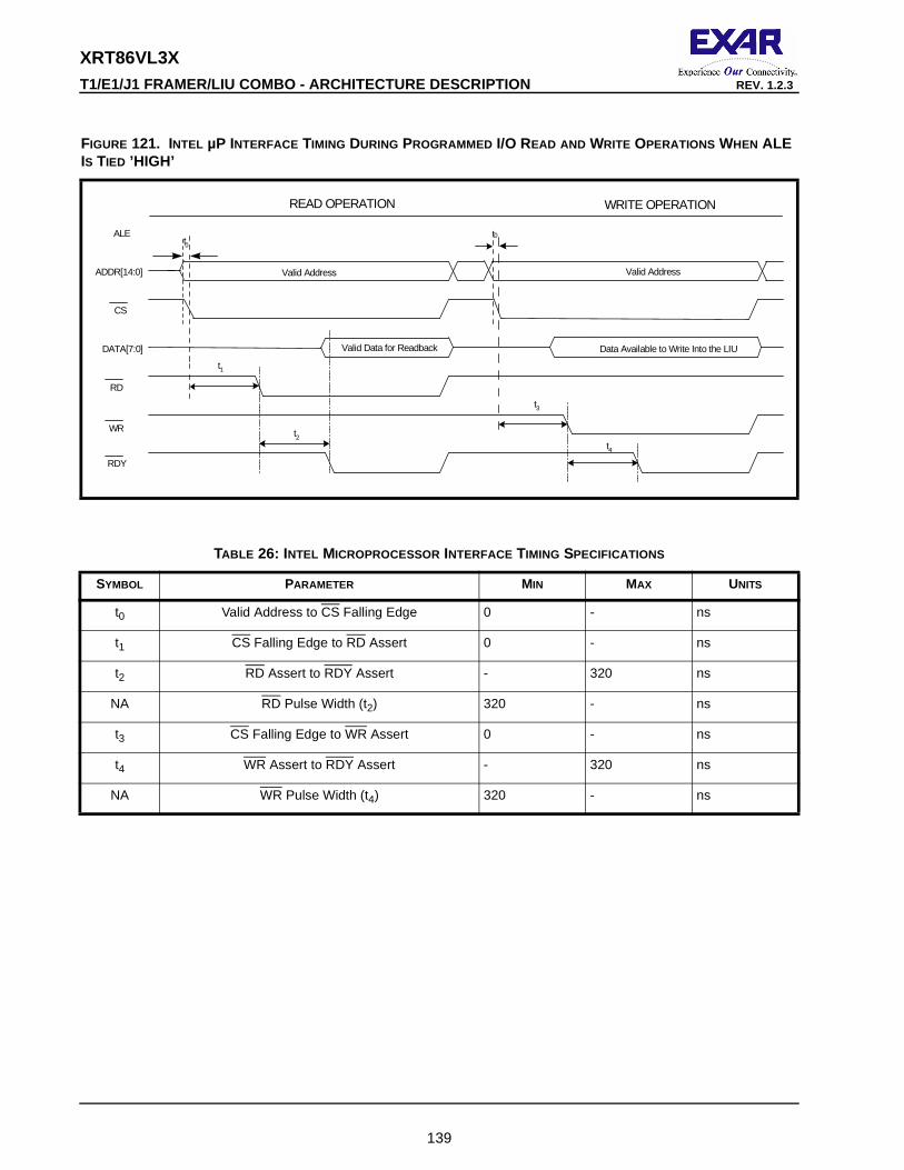
XRT86VL3X
139
T1/E1/J1 FRAMER/LIU COMBO - ARCHITECTURE DESCRIPTIO N REV. 1.2.3
FIGURE 121. INTEL µP INTERFACE TIMING DURING PROGRAMMED I/O READ AND WRITE OPERATIONS WHEN ALE IS TIED ’HIGH’
TABLE 26: INTEL MICROPROCESSOR INTERFACE TIMING SPECIFICATIONS
SYMBOL PARAMETER MIN MAX UNITS
t0 Valid Address to CS Falling Edge 0 - ns
t1 CS Falling Edge to RD Assert 0 - ns
t2 RD Assert to RDY Assert - 320 ns
NA RD Pulse Width (t2) 320 - ns
t3 CS Falling Edge to WR Assert 0 - ns
t4 WR Assert to RDY Assert - 320 ns
NA WR Pulse Width (t4) 320 - ns
CS
ADDR[14:0]
ALE
DATA[7:0]
RD
WR
RDY
Valid Data for Readback Data Available to Write Into the LIU
READ OPERATION WRITE OPERATION
t0t0
t1
t4
t2
t3
Valid Address Valid Address

XRT86VL3X
140
REV. 1.2.3 T1/E1/J1 FRAMER/LIU COMBO - ARCHITECTURE DESCRIPTIO N
MOTOROLA ASYCHRONOUS INTERFACE TIMING
The signals used in the Motorola microprocessor interface mode are: Address Strobe (AS), Data Strobe (DS), Read/Write Enable (R/W), Chip Select (CS), Address and Data bits. The interface is compatible with the timing of a Motorola 68000 microprocessor family. The interface timing is shown in Figure 122 . The I/O specifications are shown in Table 27 .
FIGURE 122. MOTOROLA ASYCHRONOUS MODE INTERFACE SIGNALS DURING PROGRAMMED I/O READ AND WRITE OPERATIONS
TABLE 27: MOTOROLA ASYCHRONOUS MODE MICROPROCESSOR INTERFACE TIMING SPECIFICATIONS
SYMBOL PARAMETER MIN MAX UNITS
t0 Valid Address to CS Falling Edge 0 - ns
t1 CS Falling Edge to DS (Pin RD_DS) Assert 0 - ns
t2 DS Assert to DTACK Assert - 320 ns
NA DS Pulse Width (t2) 320 - ns
t3 CS Falling Edge to AS (Pin ALE_AS) Falling Edge 0 - ns
CS
ADDR[6:0]
DATA[7:0]
RD_DS
WR_R/W
RDY_DTACK
Valid Data for Readback Data Available to Write Into the LIU
READ OPERATION WRITE OPERATION
t0 t0
t1
t2
Valid Address Valid Address
t3 t3
t1
t2
ALE_AS

XRT86VL3X
141
T1/E1/J1 FRAMER/LIU COMBO - ARCHITECTURE DESCRIPTIO N REV. 1.2.3
POWER PC 403 SYCHRONOUS INTERFACE TIMING
The signals used in the Power PC 403 Synchronus microprocessor interface mode are: Address Strobe (AS),Microprocessor Clock (uPCLK), Data Strobe (DS), Read/Write Enable (R/W), Chip Select (CS), Address andData bits. The interface timing is shown in Figure 123 . The I/O specifications are shown in Table 28 .
FIGURE 123. POWER PC 403 INTERFACE SIGNALS DURING PROGRAMMED I/O READ AND WRITE OPERATIONS
TABLE 28: POWER PC 403 MICROPROCESSOR INTERFACE TIMING SPECIFICATIONS
SYMBOL PARAMETER MIN MAX UNITS
t0 Valid Address to CS Falling Edge 0 - ns
t1 CS Falling Edge to WE Assert 0 - ns
t2 WE Assert to TA Assert - 320 ns
NA WE Pulse Width (t2) 320 - ns
t3 CS Falling Edge to TS Falling Edge 0 -
tdc µPCLK Duty Cycle 40 60 %
tcp µPCLK Clock Period 20 - ns
Valid Data Readback Data Available to Write into LIU
Valid AddressValid Address
t2
t1
t3
t0t0
t1
t3
t2
READ OPERATION WRITE OPERATIONTS/ALE
µµµµPCLK
ADDR[14:0]
CS
DATA[7:0]
WE
R/W
TA/RDY
tCP
tDC
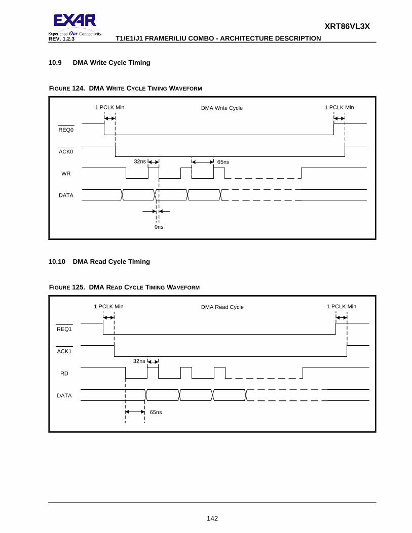
XRT86VL3X
142
REV. 1.2.3 T1/E1/J1 FRAMER/LIU COMBO - ARCHITECTURE DESCRIPTIO N
10.9 DMA Write Cycle Timing
10.10 DMA Read Cycle Timing
FIGURE 124. DMA WRITE CYCLE TIMING WAVEFORM
FIGURE 125. DMA READ CYCLE TIMING WAVEFORM
REQ0
ACK0
DMA Write Cycle
WR
DATA
1 PCLK Min 1 PCLK Min
0ns
32ns 65ns
REQ1
ACK1
DMA Read Cycle
RD
DATA
1 PCLK Min 1 PCLK Min
65ns
32ns

XRT86VL3X
143
T1/E1/J1 FRAMER/LIU COMBO - ARCHITECTURE DESCRIPTIO N REV. 1.2.3
ORDERING INFORMATION
PRODUCT NUMBER PACKAGE OPERATING TEMPERATURE RANGE
XRT86VL38IB 420 Plastic Ball Grid Array -40°C to +85°C
XRT86VL38IB484 484 Shrink Thin Ball Grid Array -40°C to +85°C
XRT86VL34IB 225 Plastic Ball Grid Array -40°C to +85°C
XRT86VL32IB 225 Plastic Ball Grid Array -40°C to +85°C

XRT86VL3X
144
REV. 1.2.3 T1/E1/J1 FRAMER/LIU COMBO - ARCHITECTURE DESCRIPTIO N
PACKAGE DIMENSIONS FOR 420 PLASTIC BALL GRID ARRAY
E 420 PLASTIC Thin Ball Grid Array (35.0 mm x 35.0 mm, PBGA)
Rev. 1.00
SYMBOL MIN MAX MIN MAXA 0.085 0.098 2.16 2.50A1 0.020 0.028 0.50 0.70A2 0.020 0.024 0.51 0.61A3 0.045 0.047 1.15 1.19D 1.370 1.386 34.80 35.20D1 1.2500 BSC 31.75 BSCE 1.370 1.386 34.80 35.20E1 1.2500 BSC 31.75 BSCb 0.024 0.035 0.60 0.90e 0.0500 BSC 1.27 TYP.
INCHES MILLIMETERS
Note: The control dimension is in millimeter.
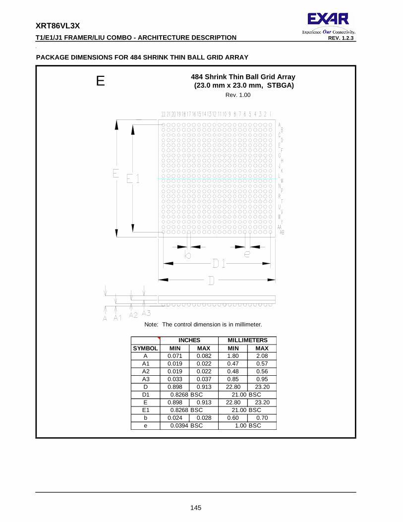
XRT86VL3X
145
T1/E1/J1 FRAMER/LIU COMBO - ARCHITECTURE DESCRIPTIO N REV. 1.2.3
4
PACKAGE DIMENSIONS FOR 484 SHRINK THIN BALL GRID AR RAY
E 484 Shrink Thin Ball Grid Array (23.0 mm x 23.0 mm, STBGA)
Rev. 1.00
SYMBOL MIN MAX MIN MAXA 0.071 0.082 1.80 2.08A1 0.019 0.022 0.47 0.57A2 0.019 0.022 0.48 0.56A3 0.033 0.037 0.85 0.95D 0.898 0.913 22.80 23.20D1 0.8268 BSC 21.00 BSCE 0.898 0.913 22.80 23.20E1 0.8268 BSC 21.00 BSCb 0.024 0.028 0.60 0.70e 0.0394 BSC 1.00 BSC
INCHES MILLIMETERS
Note: The control dimension is in millimeter.
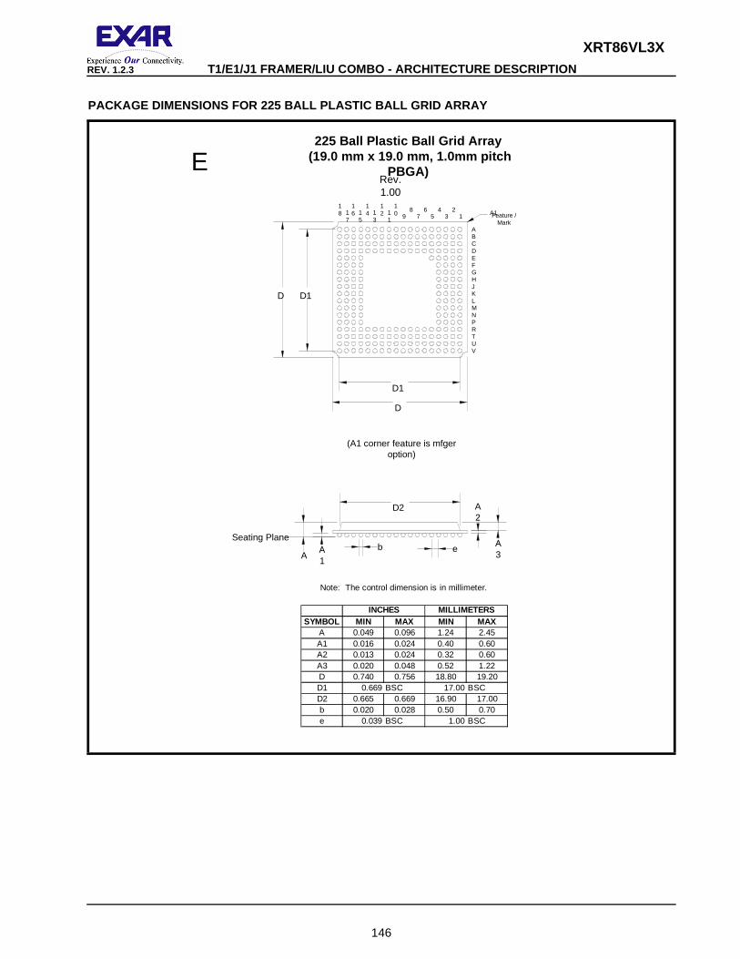
XRT86VL3X
146
REV. 1.2.3 T1/E1/J1 FRAMER/LIU COMBO - ARCHITECTURE DESCRIPTIO N
PACKAGE DIMENSIONS FOR 225 BALL PLASTIC BALL GRID A RRAY
E225 Ball Plastic Ball Grid Array
(19.0 mm x 19.0 mm, 1.0mm pitchPBGA)
Rev.1.00
SYMBOL MIN MAX MIN MAXA 0.049 0.096 1.24 2.45A1 0.016 0.024 0.40 0.60A2 0.013 0.024 0.32 0.60A3 0.020 0.048 0.52 1.22D 0.740 0.756 18.80 19.20D1 0.669 BSC 17.00 BSCD2 0.665 0.669 16.90 17.00b 0.020 0.028 0.50 0.70e 0.039 BSC 1.00 BSC
INCHES MILLIMETERS
Note: The control dimension is in millimeter.
124
378 6
517
16
141
5
121
311
10 9
18
ABCDEFGHJKLMNPRTUV
D
D1
D D1
A1Feature /Mark
D2
AA1
A2
A3
eb
(A1 corner feature is mfgeroption)
Seating Plane

147
NOTICE
EXAR Corporation reserves the right to make changes to the products contained in this publication in order toimprove design, performance or reliability. EXAR Corporation assumes no responsibility for the use of anycircuits described herein, conveys no license under any patent or other right, and makes no representation thatthe circuits are free of patent infringement. Charts and schedules contained here in are only for illustrationpurposes and may vary depending upon a user’s specific application. While the information in this publicationhas been carefully checked; no responsibility, however, is assumed for inaccuracies.
EXAR Corporation does not recommend the use of any of its products in life support applications where thefailure or malfunction of the product can reasonably be expected to cause failure of the life support system orto significantly affect its safety or effectiveness. Products are not authorized for use in such applications unlessEXAR Corporation receives, in writing, assurances to its satisfaction that: (a) the risk of injury or damage hasbeen minimized; (b) the user assumes all such risks; (c) potential liability of EXAR Corporation is adequatelyprotected under the circumstances.
Copyright 2007 EXAR Corporation
Datasheet October 2007.
Reproduction, in part or whole, without the prior written consent of EXAR Corporation is prohibited.
XRT86VL3XREV. 1.2.3 T1/E1/J1 FRAMER/LIU COMBO - ARCHITECTURE DESCRIPTIO N
REVISION HISTORY
REVISION # DATE DESCRIPTION
1.2.0 7/14/06 First release of the XRT86VL3x Architecture Description.
1.2.1 7/25/06 Corrected TA/RDY waveform in figure 119.
1.2.2 1/25/07 Changed RD to RDY delay spec in the electrical timing specs. Clarified the HDLC controller section.
1.2.3 10/15/07 Added DMA Read and Write timing waveforms in the microprocessor section of the electrical parameters.


![Cis TelePresenCo Ce isDn link...ISDN PRI Interface 1 testShutdown ISDN BRI Interface [1..4] testLoopmode ISDN BRI Interface [1..4] testPattern Cisco telePresence ISDN Link Administrator](https://img.pdfslide.us/doc/110x75/6131c5191ecc51586944f1c2/cis-telepresenco-ce-isdn-link-isdn-pri-interface-1-testshutdown-isdn-bri-interface.jpg)