Embed Size (px)
Citation preview

XPS depth profiling and leakage properties of anodized titaniadielectrics and their application in high-density capacitors
Parthasarathi Chakraborti1,2 • Himani Sharma1 • Markondeya Raj Pulugurtha1 •
Rao Tummala1
Received: 28 March 2015 / Accepted: 31 July 2015 / Published online: 6 August 2015
� Springer Science+Business Media New York 2015
Abstract The chemical structure and electrical properties
of anodized titania are investigated for their application as
conformal ultra-thin dielectrics on high surface area tita-
nium electrodes. The chemical structure is studied by XPS
depth profiling for the first time along with the role of
anodization conditions on dielectric thickness, leakage
current, and capacitance densities. Different leakage cur-
rent models were used to identify the defect mechanisms in
the titania film formed at different voltages. EDS and
structural SEM studies were performed to investigate the
morphology and structure of the titania films. This research
also demonstrates the fabrication and characterization of
high-density capacitors using high surface area titanium
metal electrodes, conformal high K, and thin-film dielectric
of titania. High-permittivity and thin-film titania dielectric
was grown on high surface area titanium anodes using
anodization, while conducting polymer was used as the
cathode. The fabricated capacitor showed 7.15 lF cm-2 at
100 kHz which corresponded to 7.5X enhancement in
surface area compared to planar thin-film capacitors. This
is the first demonstration of high-density capacitors using
high surface area titanium anodes along with high-per-
mittivity and thin-film titania as the dielectric.
Introduction
Capacitors used in the electronics industry generally fall
into two categories—traditional discretes (surface mounted
to board) and thin-film layers using substrate compatible
processes. Tantalum capacitors [1], multilayered co-fired
ceramic capacitors (MLCC) [2], and integrated passive
devices (IPDs) fall under the first category. They provide
high volumetric capacitance density at low cost, tested and
ready for board-level assembly using standard surface
mount technologies (SMT). However, they are manufac-
tured and assembled as thick components, limiting their use
in emerging high performance and miniaturized applica-
tions. The second class of capacitors comprises those that
are directly deposited as thin-film layers, providing prox-
imity advantages to active devices, while resulting in
simultaneous miniaturization. These thin-film layers are
deposited on the surface of the package substrate to form
thin-film capacitors that can be within 30–40 lm from the
active devices, while the capacitors themselves may range
from 1 to 50 lm in thickness. However, these types of
capacitors have other limitations. These include defects
that form in the capacitor process, thus affecting not only
the yield of the capacitor but also of the entire substrate. As
a result, they tend to be expensive and are not scaled up to
high-volume manufacturing. In addition, there is another
challenge related to achieving very high capacitance den-
sity with substrate compatible materials and processes. The
second type of capacitors is of more interest to emerging
high performance and miniaturized electronic systems, and
is the key focus of this paper.
The capacitance of any capacitor is given by
C ¼ Aeeot
; ð1Þ
& Himani Sharma
1 Packaging Research Center, Georgia Institute of Technology,
813 Ferst Dr, Atlanta, GA 30332, USA
2 Material Science and Engineering, Georgia Institute of
Technology, Atlanta, GA, USA
123
J Mater Sci (2015) 50:7600–7609
DOI 10.1007/s10853-015-9320-6

where e is the absolute permittivity, eo is the permittivity of
the dielectric, A is the cross-sectional area of the electrode,
and t is the thickness of the dielectric. Therefore, the
capacitance can be increased by either increasing the
electrode cross-sectional area, increasing the dielectric
constant, reducing the dielectric thickness, or by a combi-
nation of these parameters. Most substrate compatible
capacitors in the past took advantage of one or two of these
parameters. For example, silicon trench capacitors provide
high capacitance density by virtue of their high surface area
due to their high aspect ratio of through silicon vias.
However, the surface area is limited by the aspect ratio that
can be achieved and the metallization of these high aspect
ratio surfaces. In addition, the use of expensive infras-
tructure renders them non-scalable [3] for high-volume
manufacturing so as to end up with low cost. Alternative
high surface area electrode architectures have continued to
be pursued to meet higher capacitance density require-
ments. Such high surface area electrode architectures
include high surface area CNTs [4], sintered copper elec-
trodes on silicon [5], porous aluminum electrodes [6]
among others. These approaches face limitations in
achieving high capacitance density due to lower permit-
tivity of the dielectrics such as silicon dioxide (*4) and
alumina (*9). The extremely high surface area provided
by these approaches compensate for the low permittivity
and thus still result in the highest capacitance densities
reported so far. An alternative approach is to use thin films
of high K dielectrics such as barium titanate, barium
strontium titanate and their derivatives. These pose two
problems—low dielectric constant at high frequencies and
high processing temperatures to form the required dielec-
tric microstructure.
To obtain high capacitance density, it is also important
to have these high surface area architectures accessible to
the cathode or the counter electrode. For trench capacitors,
ALD TiN has been widely studied in spite of its manu-
facturability limitations mentioned earlier. Alternative low-
cost cathode options include manganese oxide [7, 8];
conducting polymers such as PEDOT:PSS [9], P3HT [10],
PANI [11], and polypyrrole [12]. They are synthesized by a
host of methods such as calcination of manganese salts,
dispensing monomer solutions for in situ polymerization,
dispensing prepolymerized suspensions, sol–gel [13]
hydrothermal and other techniques [5, 14]. Among these,
PEDOT:PSS is emerging as a favorable candidate because
of its several desirable attributes such as high conductivity
[9, 15], self-healing characteristics [16], high conformality
[17], and chemical inertness with the dielectric film. In
addition, they form oligomers on polymerization and not
big molecules; hence, they can easily penetrate inside the
high surface area architectures of the anodized anode.
All the approaches to achieve high capacitance density
can be broadly classified as those with high surface area but
low permittivity, or with high-permittivity thin films with
limited enhancement in surface area. This paper explores
an alternative approach to address both the above limita-
tions by advancing all the three parameters, high surface
area electrodes, thinner, and high-permittivity dielectrics to
increase the capacitance density, as illustrated through
Eq. (1). A schematic of this approach is shown in Fig. 1.
Commercially available porous titanium foils with high
surface area were used as the anode. The permittivity of
anodized titania ranges from 40 to 120 [18], much higher
compared to other oxide dielectrics such as alumina or
tantalum pentoxide. The self-limiting nature of anodization
process also leads to a uniform dielectric coating on the
high surface electrodes [19]. The high capacitance density
also results from thinner titania films obtained by control-
ling the anodization voltage. Prepolymerized conducting
polymer suspensions, PEDOT:PSS was used as the cath-
ode. It is important to note that the cathode may not access
the entire porous anode structure depending on the pore
and particle size. This has been highlighted in the sche-
matic. The key focus of the paper is to (a) investigate the
role of anodization conditions on capacitance density and
leakage currents, (b) elucidate the dielectric film compo-
sition along its thickness using surface analysis technique
such as XPS, (c) demonstrate higher capacitance density
with porous electrode and conformal dielectrics.
Materials and methods
High surface area anode
The high purity, commercially available porous titanium
foils (Accumet Materials, NY, USA) with thickness of
125 lm were used as the anode. The porous foils were
fabricated using powder metallurgy, involving particle
sintering at higher temperatures, to provide high surface
area of 8 m2/g (estimated using BET technique).
Fig. 1 Cross-sectional representation of the etched Ti capacitor
J Mater Sci (2015) 50:7600–7609 7601
123

High-permittivity thin-film dielectric
High-permittivity titania (TiO2) dielectric was conformally
grown over the high surface area anode using electro-
chemical anodization. An anodically grown oxide, titania,
was grown in a potentiostatic mode in dilute phosphoric
acid electrolyte with a concentration of 0.1 mM. The
anodized films were thereafter rinsed in deionized water
and dried at 100 �C for 30 min to ensure complete removal
of the electrolyte. The anodization process was performed
under a bias voltage of 10 V with respect to the cathode
(Pt) at room temperature for 30 min. The anodization
conditions are listed in Table 1.
The anodization reaction for titanium can be represented
as
Tiþ 2H2O ! TiO2 þ 2H2: ð2Þ
The thickness of the dielectric was controlled by the
anodizing voltage. A lower anodization voltage corre-
sponds to a lower driving force for the diffusion of the
oxide anions to form the dielectric oxide layer, which
culminates in the formation of a thinner dielectric. Porous
electrode capacitors were also compared with the planar
titanium electrode capacitors, fabricated under similar
conditions for their electrical properties.
Cathode
For the initial capacitance measurements, aqueous sulfuric
acid (10 wt%) was used as the counter electrode or the
cathode. For practical solid-state capacitors device, con-
ducting polymer, PEDOT:PSS (Heraeus, Leverkusen,
Germany) was chosen as the cathode. The electrode was
dispensed as a suspension of prepolymerized nanoparticles
in 5 wt% dimethyl sulfoxide (DMSO). The choice of this
liquid-based cathode was based on its ability to wet the
deep porous structures of the anodized titanium. The cho-
sen conducting polymer has a conductivity of ca.
400–600 S cm-1.
Zeiss Ultra60 FE-SEM was used for the morphological
analysis. HP 4285A precision LCR meter was used for C–
V measurements. Keithley 6485 picoammeter was used for
the leakage current analysis.
Results and discussion
Morphological characterization of high surface area
anode
The commercially acquired porous titanium anode was
studied for the pore size and morphology before and after
dielectric formation. The SEM micrograph in Fig. 2 shows
high surface area anode with pore sizes ranging from 0.5 to
20 lm. It is also evident from the micrograph that the
porous anode was fabricated by sintering the micron-sized
titanium particles that led to random pore size distribution.
The absence of through-channels results in inaccessible
surface area inside the bottom electrode architecture
implying the possibility of reduced cathode penetration
inside the porous structure. This could lead to a substantial
reduction in the capacitance density of the fabricated
structure.
Dielectric formation was carried out using anodization
of planar and high surface area titanium anode under acidic
conditions, as described earlier. Fig 3 shows the SEM
micrograph (using in-lens detector) of a cross section of
planar titanium anodized at 40 V. The thickness of the
planar anodized film at formation voltage of 40 V was
Table 1 Titanium anodization conditions
Anodization
voltage (V)
Anodization
time (min)
Temp.
(�C)Phosphoric acid
concentration (mM)
10 30 25 0.1
40 30 25 0.1
Fig. 2 SEM micrograph of porous titanium electrode
Fig. 3 SEM micrograph of a cross section of planar anodized Ti
7602 J Mater Sci (2015) 50:7600–7609
123

measured as 137.2 nm, corresponding to a rate of dielectric
formation of 3.43 nm/V. Consequently, the permittivity of
the anodized layer was estimated to be 37.59 [18, 20, 21].
The high surface area Ti anode was anodized using the
same conditions as the ones for the planar Ti. Anodization
kinetics do not change when the anodization conditions
such as anodization electrolyte and their concentration,
anodization time and voltage and temperature stay the
same. However, in a sintered electrode system, the local
field strength as well as the local ionic current density
could lead to different dielectric thickness for oxides at
different depths of the electrode [22]. Nevertheless, for the
purpose of this study, the dielectric thickness was assumed
to be the same for both the porous and the planar structures.
Anodized titanium is known to yield porous oxide which
tends to render poor dielectric properties. Thicker titanium
oxide was thus formed to reduce the dielectric porosity and
defect density [23, 24].
Chemical state characterization of the titania
dielectric
The oxide distribution in the anodized dielectric was
studied using surface sensitive XPS technique. The XPS
scans were performed at different depths of the dielectric
thickness. The scans were corrected for carbon peak elec-
trostatic charging. The depth profile was carried out using
Ar? (3 keV) ion bombardment. The sputtering rate of the
titanium oxide was estimated to be 0.07 nm/min. The
thickness of the anodized dielectric was also estimated
using the XPS depth profile and was found to be *37 nm.
It is important to note that the samples characterized using
XPS were anodized with 8 V and estimated to have
34.3-nm dielectric thickness.
The survey scans of TiO2 film at three different depths
are shown in Fig. 4. The evolution of Ti and decrease of
oxygen peaks is clearly seen along the depth of the
dielectric thickness. The presence of P in the initial layers
of the dielectric is also evident from the scans. Incorpo-
ration of P in anodized films is known to occur with
phosphoric acid as electrolyte [25]. It is also expected to
yield lower ionic conductivity [26]. As we move along the
film thickness, the phosphorus percentage comes down
from 10 % (at etch depth of 2.8 nm) to almost negligible
amount (at etch depth of 12.6 nm). This differs from the
phosphorus incorporation in Ta2O5 where the phosphorus
concentration is same till halfway through the film thick-
ness. Beyond the halfway thickness no further phosphorous
is observed in case of tantalum [25]. Peak at 978 eV
belongs to the Auger peak of oxygen.
Figure 5 shows the core level scans of Ti at different
etch depths. Ti 4p core level scans appear as a doublet at
459 eV(4p1/2) and 465 eV (4p3/2) that tend to shift to 454
and 460 eV, respectively with increasing sputtering depth.
The peak shifts at lower binding energies with the
increasing etching depth clearly show the evolution of Ti
from higher oxidation states to purely metallic. The pres-
ence of broad peak, instead of resolved Ti doublet at
16.8 nm (sputtered depth level) indicates the existence of
different Ti suboxides which later emerge as a clear dou-
blet around 40 nm of sputtered depth.
The Ti suboxides were elucidated by deconvoluting the
acquired scans at each level with Guassian components
using standard FWHM and position from known valence
states. The de-convoluted peaks at each level are shown in
Fig. 6.
The surface of the TiO2 was dominated by Ti (?4) state
which is also significantly present in the middle of the
dielectric thickness (16 nm). The peak at binding energy
458.8 eV corresponds to Ti4?. The de-convolution also
demonstrates the presence of non-stoichiometric oxides of
Ti (depicted as Tix?) at different depths of the oxide. Trace
amount of Ti in oxidation state ?2 can be seen near the
surface which rises as we again go down along the depth of
TiO2 film. The distribution of the oxides in the dielectric is
summarized using a depth profile plot in Fig. 7 where the
Fig. 4 Survey scans of Ti at different etch depths Fig. 5 Ti Core level scans of TiO2 films at different etch depths
J Mater Sci (2015) 50:7600–7609 7603
123

percentages of Ti in different oxidation states are plotted at
different etch depths. It is interesting to note that the all the
oxidation states are present in almost equal quantities
around 20 nm depth, beyond which the oxide content drops
to less than 0.1 %. Thus, the Ti4? oxide is primarily pre-
sent at the surface of the anodized titanium film and a mix
of oxides are observed at intermittent and lower depths.
The emergence of non-stoichiometric oxides along with
lower valence oxides like Ti2? indicates that the thermo-
dynamics/kinetics or both of the dielectric formation
changes along the anodized thickness.
Thermodynamically, Gibbs energy favors the reduction
of titania when in contact with a metal (in this case Ti) as
given by the Eq. (2)
Tiþ TiO2 ! TiOx þ TiO2�x: ð2Þ
This could explain the presence of suboxides near the
metal/oxide interface.
Anodization kinetics of titanium predicts the formation
of anodic film through the outward diffusion of the tita-
nium cations and inward diffusion of oxide anions. Titania
is known to exist in amorphous phase in the outer part of
the anodic oxide film (near/at the oxide/electrolyte inter-
face) which is further stabilized by the incorporation of
electrolyte-derived species such as phosphorous corrobo-
rated by our XPS study. This is accompanied by the
amorphous to crystalline phase transition yielding a crys-
talline titania layer underneath (near/at the oxide/metal),
instances of which have been reported in literature at
anodization bias as low as 5 V [27–30]. Oxide ions could
migrate faster along the open channels of amorphous oxide
structure while they diffuse along slower paths via vacan-
cies [31]. Lower oxide mobility yields oxygen deficiency in
those regions that manifests as non-stoichiometric oxides
or titanium oxides with titanium in lower oxidation states.
Conversely, higher oxide mobility would lead to Ti oxide
with Ti in its highest oxidation states. The XPS data evince
the Ti4? at the top of anodic oxide film, while the non-
stoichiometric oxides and Ti2? are present underneath.
With grain sizes, ca. 1 nm, the porous crystalline phase
heavily contributes to the leakage conduction in titania
dielectric [28]. The above discussion as well as the XPS
study further suggests that the amorphous titania comprises
of stoichiometric oxides, whereas crystalline titania yields
non-stoichiometric oxides.
Valence band spectra of TiO2 at different etch depths are
shown in Fig. 8. The presence of poorly formed Fermi
level at the surface is typical for a dielectric and is clearly
seen at etch depth of 2.8 nm in Fig. 8. This shows that the
surface is dominant with insulating titanium oxide layer.
As the etch depth increases, the Fermi level gets more
pronounced due to higher carrier density at the Fermi level.
This is possible only when the valence band is above the
Fig. 6 De-convoluted peaks of Ti showing Ti and its oxides at
various etched depths
Fig. 7 Depth profile of Ti in different oxidation states along
dielectric thickness
7604 J Mater Sci (2015) 50:7600–7609
123

Fermi level which indicates the presence of Ti metal at etch
depths of 37 nm. Hence, XPS core level and valence band
results corroborate each other with dielectric thickness of
37 nm. Valence band states in between the titanium oxide
and Ti metal represent a contribution of different Ti sub-
oxides dominant at different etch levels. Valence band
spectra could be used to glean information on the band gap
of the oxide. The binding energy axis intercept of the
tangent drawn at the inflexion point of the valence band
spectra is a function of the band gap. The binding energy
intercept diminishes away near the Ti/TiO2 interface (the
intercept with the binding energy axis is negative). A
negative intercept is observed for the valence spectra at
etch depth of 37.8 nm which could be ascribed to the
presence of valence band near or above the Fermi Level.
This indicates the presence of metallic Ti near the Ti/TiO2
interface which is consistent with the observations men-
tioned from the analyses above.
Cathode infiltration inside the high surface area anodized
electrode
The infiltration of the conducting polymer inside the porous
regions of the anodized Ti anode was validated by per-
forming an EDS (not shown here) at the very bottom of the
porous Ti. The presence of carbon and sulfur, which form
the PEDOT backbone chain, at a depth of 125 lm from the
top surface in the Ti electrode confirmed the penetration of
conducting polymer. Strong oxygen signals obtained from
the same region could be attributed to both the titania film
and the conducting polymer counter electrode.
Electrical characterization
Planar thin-film capacitors
The capacitance density for planar films registered a
decrease from 0.97 to 0.43 lF cm-2 as the formation
voltage was increased from 10 to 40 V. This dip in
capacitance density stems from thicker dielectric formed at
higher anodization voltages, which reduces the capacitance
governed by Eq. (1). However, the dielectric quality
improves with thicker dielectrics. Figure 9 shows the nor-
malized I–V plot for capacitors (with metal as top elec-
trode) with formation voltages of 10 and 40 V. As can be
seen from the figure, the thicker dielectric showed lower
leakage current even at higher voltage as compared to
thinner dielectric because of the relatively lower defect
density.
The presence of thicker dielectric reduces the leakage
current from 146 to 11 nA nF-1 as the formation voltage
was raised from 10 to 40 V. Thinner dielectrics as com-
pared to thicker ones are more prone to pin holes and other
defects, leading to much higher leakage current.
The defect mechanisms in the formed dielectric at 10
and 40 V were analyzed using five known classical leakage
mechanisms—Schottky effect, Poole–Frenkel effect, ion
hopping mechanism, space charge limited conduction
(SCLC), and Fordheim Nordler Tunneling (FNT)
mechanism.
Schottky conduction mechanism corresponds to the
lowering of energy barrier due to thermal excitation of
electrons across the metal–dielectric interface [5]. The
leakage current flow attributed to Schottky mechanism [32]
is given by
lnðJsÞ ¼1
2KTb
ffiffiffiffi
Ep
þ ln A�T2� �
� qus
KT
h i
;
where, Js is the current density, E is the electric field, A* is
the Richardson constant, T: absolute temperature, Us is the
barrier height, K is the Boltzman’s constant, b is a material
constant given by
b ¼
ffiffiffiffiffiffiffiffiffiffi
q3
Peeo
s
;
where e is the relative permittivity at high frequency
(optical dielectric constant), eo is the permittivity in vac-
uum, and q is the elementary charge. Optical dielectric
Fig. 8 Valence band of Ti oxides at near surface and near the Ti–
TiO2 interface Fig. 9 I–V curve for planar titanium capacitor
J Mater Sci (2015) 50:7600–7609 7605
123

constant is used for the sake of calculation since the
dielectric relaxation time is slower than the electron resi-
dence time in the dielectric [33]. Defects in the titania
dielectric would be dominated by Schottky electronic
conduction mechanism if the plot of ln(Js) versus HE is
linear with slope close to 5.5E-04 assuming an optical
dielectric constant of 7.29 [34]. In Fig. 10a, the experi-
mental data for both 10 and 40 V anodized dielectric fit the
characteristic Schottky plots quite well. However, the
slopes for both thinner (3.3E-04) and thicker (4.97E-04)
dielectrics register a mismatch compared to the theoreti-
cally calculated slope of 5.5E-04. Hence, it can be infer-
red that none of the dielectrics exhibit Schottky conduction
mechanisms. This can be supported by the band diagram
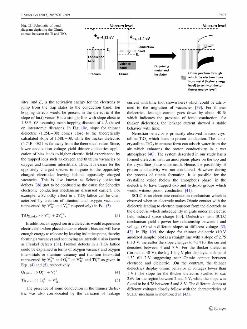
near the Ti-TiO2 interface (Fig. 11) where the electrons in
the Ti metal on contact between the metal and the oxide
layer would lower their energy by transporting from con-
duction band of the metal to the conduction band of the
oxide and vice versa, thus, yielding an Ohmic contact and
no Schottky barrier [35, 36].
For further understanding the leakage current mecha-
nism Poole–Frenkel mechanism was analyzed that involves
electron hopping from a trapped site in the dielectric
(created by an ion vacancy) into its conduction band of the
dielectric under applied electric field [33]. Leakage current
attributed to Frenkel Poole Mechanism [32] is given by
lnJPF
E¼ b
fKT
ffiffiffiffi
Ep
þ ln Cð Þ � qus
fkt
� �
;
where JPF is the current density, C is a proportionality
constant, and f can take a value between 1 and 2 and is a
function of the acceptor compensation in the material.
Frenkel Poole effects dominate the defects in dielectric if
the plot of ln (JPF/E) versus HE is a straight line and the
value of f falls between 1 and 2. In Fig. 10b, the value of ffor thinner dielectric is 5.4, while the f value for thicker
dielectric is 2.6, both of which falls outside the theoretical
range of calculated values of f. Hence, Poole–Frenkel
conduction as a leakage mechanism could not account as
the dominant mechanism for the leakage current in the
titania dielectric.
Ionic conduction as a defect mechanism could be
attributed to the hopping of vacancies such as oxygen
vacancies/interstitials and titanium ion/interstitials vacan-
cies within the dielectric [37]. The current attributed to ion
hopping [33] is given by
lnðJÞ ¼ qa
KTE þ lnðqanmÞ � Ea
KT
� �
;
where a is the mean hopping distance of the ions, n is the
electron concentration in conduction band, t is the fre-
quency of thermal vibration of electrons at the trapped
Fig. 10 Defect mechanism
a Schottky effect, b Poole–
Frenkel effect, c Ion hopping
mechanism, d SCLC
mechanism of planar titanium
dielectrics
7606 J Mater Sci (2015) 50:7600–7609
123
sites, and Ea is the activation energy for the electrons to
jump from the trap states to the conduction band. Ion
hopping defects would be present in the dielectric if the
slope of ln(J) versus E is a straight line with slope close to
1.58E-08 assuming mean hopping distance of 4 A (based
on interatomic distance). In Fig. 10c, slope for thinner
dielectric (1.25E-08) comes close to the theoretically
calculated slope of 1.58E-08, while the thicker dielectric
(4.74E-08) lies far away from the theoretical value. Since,
lower anodization voltage yield thinner dielectrics appli-
cation of bias leads to higher electric field experienced by
the trapped ions such as oxygen and titanium vacancies or
oxygen and titanium interstitials. Thus, it is easier for the
oppositely charged species to migrate to the oppositely
charged electrodes leaving behind oppositely charged
vacancies. This is also known as Schottky ionization
defects [38] (not to be confused as the cause for Schottky
electronic conduction mechanism discussed earlier). For
example, a Schottky effect in a TiO2 lattice can be char-
acterized by creation of titanium and oxygen vacancies
represented by VTi4- and Vo
2? respectively) in Eq. (3)
TiO2Lattice , V4�Ti þ 2V2þ
o : ð3Þ
In addition, a trapped ion in a dielectric would experience
electric fieldwhen placed under an electric bias andwill have
enough energy to relocate by leaving its lattice point, thereby
forming a vacancy) and occupying an interstitial also known
as Frenkel defects [38]. Frenkel defects in a TiO2 lattice
could be explained in terms of oxygen vacancy and oxygen
interstitials or titanium vacancy and titanium interstitial
represented by Vo2? and Oi
2- or VTi4- and Tii
4? as given in
Eqs. (4) and (5), respectively
OLattice , O2�i þ V2þ
o ð4Þ
TiLattice , Ti4þi þ V4�Ti : ð5Þ
The presence of ionic conduction in the thinner dielec-
tric was also corroborated by the variation of leakage
current with time (not shown here) which could be attrib-
uted to the migration of vacancies [39]. For thinner
dielectrics, leakage current goes down by about 40 %
which indicates the presence of ionic conduction; for
thicker dielectrics, the leakage current showed a stable
behavior with time.
Nernstian behavior is primarily observed in nano-crys-
talline TiO2 which leads to proton conduction. The nano-
crystalline TiO2 in anatase form can adsorb water from the
air which enhances the proton conductivity in a wet
atmosphere [40]. The system described in our study has a
formed dielectric with an amorphous phase on the top and
the crystalline phase underneath. Hence, the possibility of
proton conductivity was not considered. However, during
the process of titania formation, it is possible for the
crystalline oxide (below the amorphous phase) in the
dielectric to have trapped oxo and hydroxo groups which
would witness proton conduction [41].
SCLC is an electronic conduction mechanism which is
observed when an electrode makes Ohmic contact with the
dielectric leading to electron transport from the electrode to
the dielectric which subsequently migrate under an electric
field induced space charge [33]. Dielectrics with SCLC
mechanism yield a power law relationship between J and
voltage (V) with different slopes at different voltage [33,
42]. In Fig. 10d, the slope for thinner dielectric (10 V
anodized sample) plot is a straight line with a slope of 2.75
till 3 V, thereafter the slope changes to 4.14 for the current
densities between 4 and 7 V. For the thicker dielectric
(formed at 40 V), the log J–log V plot displayed a slope of
1.32 till 2 V suggesting near Ohmic contact between
electrode and dielectric. (On the contrary, the thinner
dielectrics display ohmic behavior at voltages lower than
1 V.) The slope for the thicker dielectric swelled to c.a.
2.69 for the region between 2 and 5 V, while the slope was
found to be 4.78 between 5 and 8 V. The different slopes at
different voltages closely follow with the characteristics of
SCLC mechanism mentioned in [43].
Fig. 11 Schematic of band
diagram depicting the Ohmic
contact between the Ti and TiO2
J Mater Sci (2015) 50:7600–7609 7607
123

FNT conduction mechanism corresponds to the tunnel-
ing of electrons through the potential barrier into the con-
duction band of the dielectric even though the energy of the
incident electron is less than the potential barrier. FNT
conduction dominates when a plot of ln(J) versus 1/E is a
straight line. FNT is usually observed at very high applied
electric field or with dielectrics thinner than 10 nm. Since
the dielectric thickness in this study is much greater than
10 nm, FNT mechanism would not hold true [33].
In summary, the thinner dielectrics showed a combina-
tion of ionic and trap-enhanced SCLC, while thicker
dielectrics showed Schottky conduction. However, it is
highly likely that multiple conduction mechanisms co-
exist.
High surface area capacitors
A capacitance density of 39 lFcm-2 was measured using
liquid cathodes. The liquid electrolyte penetrates the por-
ous electrode and accesses the total surface area, resulting
in a maximum capacitance density. The inability of the
polymers to reach all the crevices in the porous network
renders lower capacitance density. The fabricated capacitor
devices with PEDOT–PSS yielded a capacitance density of
7.15 lFcm-2 which corresponds to a surface area
enhancement of 7.5X for the high surface area titanium
anode as compared to planar titanium devices (shown in
Table 2). The area enhancement is estimated based on an
oxide thickness of 34.3 nm for planar samples for the 10 V
anodization. The capacitance density can be further
improved by modifying the bottom electrode structure to
give higher surface area with open pores and higher
porosity. The capacitance density would also increase with
better infiltration of conducting polymers into the porous
structure.
The leakage current of the high surface area capacitor,
as shown in Fig. 12, was found to be higher than those
measured with aluminum-based capacitors [5, 24]. The
results corroborate with the high leakage in titania reported
earlier by Burns [44] and Tanvir et al. [18]. The presence of
defects such as thinner dielectric spots, lower interfacial
barrier because of lower work function of Ti electrodes
leading to Schottky conduction, lattice defects such as
Schottky and Frenkel defects (described earlier) causing
ionic conduction, trap-enhanced SCLC, and pin holes in
anodized oxide films could be attributed to the high leakage
current in the titania film. The conformal nature of
dielectric formed by anodization could also lead to higher
built-in stresses in the dielectric in a high surface area
titanium capacitor. The stresses could lead to subsequent
cracks in the dielectric during capacitor operation at higher
voltages. This could account for the high leakage current in
the high surface area capacitor as compared to the planar
titanium capacitors. Further improvement in the anodiza-
tion conditions and cathode processing to invoke self-
healing can lower the leakage currents.
Conclusions
This paper describes new materials and structures to
enhance the capacitance density by advancing all the three
parameters that affect the capacitance: surface area, per-
mittivity, and thinness of dielectric. An initial proof-of-
concept was demonstrated with porous titanium electrodes.
The porous titanium capacitors were benchmarked with
planar titanium capacitors. A leakage current of
10 nA nF-1 was achieved with higher anodization voltages
for planar titanium capacitors while retaining a planar
capacitance density of 0.44 lF cm-2. Various leakage
conduction mechanisms were analyzed using different
models to account for difference in leakage currents in
thinner and thicker dielectrics. The thinner dielectrics
showed a combination of ionic and trap-enhanced SCLC,
while thicker dielectrics showed Schottky. XPS depth
profile and valence band spectra confirmed the presence of
Ti oxide as Ti(4?) near the surface, while mixed oxides
were observed at intermittent depths which contributes to
the poor dielectric properties. Capacitance density of
7.15 lF cm-2 and 7.5X area enhancement over planar foils
was achieved with solid cathodes. More process opti-
mization is required with solid cathodes to yield higher
capacitance and lower leakage currents.
Table 2 Area enhancement using porous Ti v planar Ti
Planar thin film Porous thickfilm
Cap density (lF cm-2) 0.97 39 (liquid)
7.15 (PEDOT–PSS)
Area enhancement (X) 1 40 (liquid)
*7.5 (PEDOT–PSS)
Fig. 12 I–V characterization for porous titanium capacitor
7608 J Mater Sci (2015) 50:7600–7609
123

Acknowledgements The authors would also like to thank Prof.
Walton and her research group, Georgia Institute of Technology for
their assistance with the BET measurements and Eric Woods,
Microelectronics Research Center, Georgia Institute of Technology
for his assistance with SEM.
References
1. Freeman Y et al (2009) Electrical characterization of tantalum
capacitors with poly (3, 4-ethylenedioxythiophene) counter
electrodes. J Electrochem Soc 156(6):G65–G70
2. Maher G (1985) Improved dielectrics for multilayer ceramic
capacitors. Electron Power 31(8):567–569
3. Hoogeland D et al (2009) Plasma-assisted atomic layer deposition
of TiN/Al2O3 stacks for metal-oxide-semiconductor capacitor
applications. J Appl Phys 106(11):114107–114107-7
4. Budnik M et al (2006) A high density, carbon nanotube capacitor
for decoupling applications. In: Proceedings of the 43rd annual
design automation conference. ACM, New York
5. Sharma H et al (2012) Fabrication and characterization of novel
silicon-compatible high-density capacitors. J Mater Sci Mater
Electron 23(2):528–535
6. Raj PM et al (2011) Thin film power components with nanoscale
electrodes and conformal dielectrics. In: 2011 11th IEEE con-
ference on nanotechnology (IEEE-NANO). IEEE, Portland
7. Preisler E (1976) Semiconductor properties of manganese diox-
ide. J Appl Electrochem 6(4):311–320
8. Wei W et al (2011) Manganese oxide-based materials as elec-
trochemical supercapacitor electrodes. Chem Soc Rev 40(3):
1697–1721
9. Elschner A, Kirchmeyer S (2008) PEDOT-type materials in
organic solar cells. In: Organic photovoltaics, pp 211–242
10. Lee SH et al (2011) Tuning optical properties of poly (3-
hexylthiophene) nanoparticles through hydrothermal processing.
Sci Technol Adv Mater 12(2):025002
11. Wan M (2008) Conducting polymers with micro or nanometer
structure. Springer, Berlin
12. Larmat F, Reynolds JR, Qiu Y-J (1996) Polypyrrole as a solid
electrolyte for tantalum capacitors. Synth Met 79(3):229–233
13. Sadekar AG et al (2012) Robust PEDOT films by covalent
bonding to substrates using in tandem sol–gel, surface initiated
free-radical and redox polymerization. J Mater Chem 22(1):
100–108
14. Sethi K et al (2011) Conformal atomic layer deposition (ALD) of
alumina on high surface-area porous copper electrodes to achieve
ultra-high capacitance density on silicon interposers. In: 2011
IEEE 61st electronic components and technology conference
(ECTC), IEEE, Lake Buena Vista
15. Louwet F et al (2003) PEDOT/PSS: synthesis, characterization,
properties and applications. Synth Met 135:115–117
16. Prymak J (2001) Improvements with polymer cathodes in alu-
minum and tantalum capacitors. In: Proceedings of the 16th
applied power electronics conference and exposition
17. Pulugurtha M et al (2011) Systems and methods for providing
high-density capacitors. Google patents
18. Tanvir MT et al (2011) Dielectric properties of anodic films on
sputter-deposited Ti–Si porous columnar films. Appl Surf Sci
257(19):8295–8300
19. Poinern GEJ, Ali N, Fawcett D (2011) Progress in nano-engi-
neered anodic aluminum oxide membrane development. Materi-
als 4(3):487–526
20. Feuersanger A (1964) Titanium-dioxide dielectric films prepared
by vapor reaction. Proc IEEE 52(12):1463–1465
21. Wypych A et al (2014) Dielectric properties and characterisation
of titanium dioxide obtained by different chemistry methods.
J Nanomater. doi:10.1155/2014/124814
22. Lohrengel M et al (2013) Oxide Films on sintered tantalum for
electrolytic capacitors. J Electrochem Plating Tech. doi:10.
12850/ISSN2196-0267.JEPT4750
23. Sharma H et al (2013) 7 Package-compatible high-density nano-
scale capacitors with conformal nano-dielectrics. In: Nanoelec-
tronic device applications handbook, p 79
24. Lin H, Ye P, Wilk G (2005) Leakage current and breakdown
electric-field studies on ultrathin atomic-layer-deposited Al2O3
on GaAs. Appl Phys Lett 87(18):182904–182904-3
25. Sloppy JD et al (2010) Complex dielectric functions of anodic bi-
layer tantalum oxide. Electrochim Acta 55(28):8751–8757
26. Randall J Jr (1975) The effect of phosphorus incorporation on the
dielectric constant and ionic conductivity of anodic tantalum
oxide. Electrochim Acta 20(9):663–667
27. Habazaki H et al (2002) Influence of molybdenum species on
growth of anodic titania. Electrochim Acta 47(24):3837–3845
28. Habazaki H et al (2003) Crystallization of anodic titania on
titanium and its alloys. Corros Sci 45(9):2063–2073
29. Li Q (2013) Titanium dioxide dielectric layers made by
anodization of titanium: the effect of dissolved nitrogen and
oxygen. Case Western Reserve University, Cleveland
30. Aladjem A (1973) Anodic oxidation of titanium and its alloys.
J Mater Sci 8(5):688–704. doi:10.1007/BF00561225
31. Gleaves G, Dearnaley G, Collins R (1986) A phenomenological
model for the anodization of titanium. Thin Solid Films
135(1):L5–L8
32. Alapatt G et al (2010) Observation of the Poole–Frenkel effect in
tantalum polymer capacitors. In: Proceedings of the IEEE
SoutheastCon 2010, pp 498–501
33. Chiu F-C (2014) A review on conduction mechanisms in
dielectric films. Adv Mater Sci Eng. doi:10.1155/2014/578168
34. Liu F-M, Wang T-M (2002) Surface and optical properties of
nanocrystalline anatase titania films grown by radio frequency
reactive magnetron sputtering. Appl Surf Sci 195(1):284–290
35. Diebold U (2003) The surface science of titanium dioxide. Surf
Sci Rep 48(5):53–229
36. Kasap SO (2006) Principles of electronic materials and devices.
McGraw-Hill, New York
37. Amin M et al (1991) Study of the conduction mechanisms in
polycarbonate. Die Angew Makromol Chem 193(1):13–20
38. Kurnick S (1952) The effects of hydrostatic pressure on the ionic
conductivity of AgBr. J Chem Phys 20(2):218–228
39. Markondeya Raj P et al (2010) Hydrothermal barium titanate
thin-film characteristics and their suitability as decoupling
capacitors. J Am Ceram Soc 93(9):2764–2770
40. Eppler AM, Ballard IM, Nelson J (2002) Charge transport in
porous nanocrystalline titanium dioxide. Phys. E 14(1):197–202
41. Lyon LA, Hupp JT (1999) Energetics of the nanocrystalline
titanium dioxide/aqueous solution interface: approximate con-
duction band edge variations between H0 = -10 and H- = ?26.
J Phys Chem B 103(22):4623–4628
42. Wagle S, Shirodkar V (2000) Space-charge-limited conduction in
thin film Al/Sb2Pb1Se7/Al devices. Braz J Phys 30(2):380–385
43. Rose A (1955) Space-charge-limited currents in solids. Phys Rev
97(6):1538
44. Burns G (1989) Titanium dioxide dielectric films formed by rapid
thermal oxidation. J Appl Phys 65(5):2095–2097
J Mater Sci (2015) 50:7600–7609 7609
123