Embed Size (px)
Citation preview
XIO2213BXIO2213BPCI Express™ TO 1394b OHCI WITH 3-PORT PHY
Data Manual
PRODUCTION DATA information is current as of publication date.Products conform to specifications per the terms of the TexasInstruments standard warranty. Production processing does notnecessarily include testing of all parameters.
Literature Number: SCPS210F
October 2008–Revised May 2013
XIO2213B
www.ti.com SCPS210F –OCTOBER 2008–REVISED MAY 2013
Contents1 Introduction ...................................................................................................................... 12
1.1 XIO2213B Features ....................................................................................................... 122 Overview .......................................................................................................................... 13
2.1 Related Documents ....................................................................................................... 142.2 Documents Conventions ................................................................................................. 152.3 Ordering Information ...................................................................................................... 152.4 Terminal Assignments .................................................................................................... 162.5 Terminal Descriptions ..................................................................................................... 24
3 Feature/Protocol Descriptions ............................................................................................. 313.1 Power-Up/Power-Down Sequencing .................................................................................... 31
3.1.1 Power-Up Sequence ........................................................................................... 323.1.2 Power-Down Sequence ........................................................................................ 33
3.2 XIO2213B Reset Features ............................................................................................... 343.3 PCI Express (PCIe) Interface ............................................................................................ 35
3.3.1 External Reference Clock ..................................................................................... 353.3.2 Beacon and Wake .............................................................................................. 353.3.3 Initial Flow Control Credits .................................................................................... 353.3.4 PCIe Message Transactions .................................................................................. 36
3.4 PCI Interrupt Conversion to PCIe Messages .......................................................................... 373.5 Two-Wire Serial-Bus Interface ........................................................................................... 38
3.5.1 Serial-Bus Interface Implementation ......................................................................... 383.5.2 Serial-Bus Interface Protocol .................................................................................. 393.5.3 Serial-Bus EEPROM Application ............................................................................. 413.5.4 Accessing Serial-Bus Devices Through Softwaree ........................................................ 43
3.6 Advanced Error Reporting Registers ................................................................................... 433.7 Data Error Forwarding Capability ....................................................................................... 433.8 General-Purpose I/O (GPIO) Interface ................................................................................. 443.9 Set Slot Power Limit Functionality ...................................................................................... 443.10 PCIe and PCI Bus Power Management ................................................................................ 443.11 1394b OHCI Controller Functionality ................................................................................... 46
3.11.1 1394b OHCI Power Management ............................................................................ 463.11.2 1394b OHCI and V AUX ........................................................................................ 463.11.3 1394b OHCI and Reset Options .............................................................................. 463.11.4 1394b OHCI PCI Bus Master ................................................................................. 463.11.5 1394b OHCI Subsystem Identification ....................................................................... 473.11.6 1394b OHCI PME Support .................................................................................... 47
4 Classic PCI Configuration Space ......................................................................................... 484.1 Vendor ID Register ........................................................................................................ 494.2 Device ID Register ........................................................................................................ 494.3 Command Register ........................................................................................................ 494.4 Status Register ............................................................................................................ 514.5 Class Code and Revision ID Register .................................................................................. 524.6 Cache Line Size Register ................................................................................................ 524.7 Primary Latency Timer Register ......................................................................................... 524.8 Header Type Register .................................................................................................... 534.9 BIST Register .............................................................................................................. 534.10 Device Control Base Address Register ................................................................................. 534.11 Scratchpad RAM Base Address ......................................................................................... 544.12 Primary Bus Number Register ........................................................................................... 544.13 Secondary Bus Number Register ....................................................................................... 544.14 Subordinate Bus Number Register ...................................................................................... 55
2 Contents Copyright © 2008–2013, Texas Instruments Incorporated
XIO2213B
www.ti.com SCPS210F –OCTOBER 2008–REVISED MAY 2013
4.15 Secondary Latency Timer Register ..................................................................................... 554.16 I/O Base Register ......................................................................................................... 554.17 I/O Limit Register .......................................................................................................... 564.18 Secondary Status Register ............................................................................................... 574.19 Memory Base Register ................................................................................................... 584.20 Memory Limit Register .................................................................................................... 584.21 Prefetchable Memory Base Register ................................................................................... 594.22 Prefetchable Memory Limit Register .................................................................................... 594.23 Prefetchable Base Upper 32 Bits Register ............................................................................. 604.24 Prefetchable Limit Upper 32 Bits Register ............................................................................. 604.25 I/O Base Upper 16 Bits Register ........................................................................................ 614.26 I/O Limit Upper 16 Bits Register ......................................................................................... 614.27 Capabilities Pointer Register ............................................................................................. 624.28 Interrupt Line Register .................................................................................................... 624.29 Interrupt Pin Register ..................................................................................................... 624.30 Bridge Control Register ................................................................................................... 634.31 PM Capability ID Register ................................................................................................ 654.32 Next Item Pointer Register ............................................................................................... 654.33 Power Management Capabilities Register ............................................................................. 664.34 Power Management Control/Status Register .......................................................................... 674.35 Power Management Bridge Support Extension Register ............................................................ 684.36 Power Management Data Register ..................................................................................... 684.37 MSI Capability ID Register ............................................................................................... 684.38 Next Item Pointer Register ............................................................................................... 694.39 MSI Message Control Register .......................................................................................... 694.40 MSI Message Lower Address Register ................................................................................. 704.41 MSI Message Upper Address Register ................................................................................. 704.42 MSI Message Data Register ............................................................................................. 714.43 SSID/SSVID Capability ID Register ..................................................................................... 714.44 Next Item Pointer Register ............................................................................................... 714.45 Subsystem Vendor ID Register .......................................................................................... 724.46 Subsystem ID Register ................................................................................................... 724.47 PCI Express Capability ID Register ..................................................................................... 724.48 Next Item Pointer Register ............................................................................................... 724.49 PCI Express Capabilities Register ...................................................................................... 734.50 Device Capabilities Register ............................................................................................. 744.51 Device Control Register .................................................................................................. 754.52 Device Status Register ................................................................................................... 764.53 Link Capabilities Register ................................................................................................ 774.54 Link Control Register ...................................................................................................... 784.55 Link Status Register ....................................................................................................... 794.56 Serial-Bus Data Register ................................................................................................. 794.57 Serial-Bus Word Address Register ...................................................................................... 794.58 Serial-Bus Slave Address Register ..................................................................................... 804.59 Serial-Bus Control and Status Register ................................................................................ 814.60 GPIO Control Register .................................................................................................... 824.61 GPIO Data Register ....................................................................................................... 834.62 Control and Diagnostic Register 0 ...................................................................................... 844.63 Control and Diagnostic Register 1 ...................................................................................... 864.64 PHY Control and Diagnostic Register 2 ................................................................................ 874.65 Subsystem Access Register ............................................................................................. 884.66 General Control Register ................................................................................................. 884.67 TI Proprietary Register .................................................................................................... 91
Copyright © 2008–2013, Texas Instruments Incorporated Contents 3
XIO2213B
SCPS210F –OCTOBER 2008–REVISED MAY 2013 www.ti.com
4.68 TI Proprietary Register .................................................................................................... 914.69 TI Proprietary Register .................................................................................................... 914.70 Arbiter Control Register ................................................................................................... 924.71 Arbiter Request Mask Register .......................................................................................... 934.72 Arbiter Time-Out Status Register ........................................................................................ 944.73 TI Proprietary Register .................................................................................................... 954.74 TI Proprietary Register .................................................................................................... 954.75 TI Proprietary Register .................................................................................................... 95
5 PCIe Extended Configuration Space .................................................................................... 965.1 Advanced Error Reporting Capability ID Register ..................................................................... 965.2 Next Capability Offset/Capability Version Register ................................................................... 975.3 Uncorrectable Error Status Register .................................................................................... 975.4 Uncorrectable Error Mask Register ..................................................................................... 985.5 Uncorrectable Error Severity Register .................................................................................. 995.6 Correctable Error Status Register ..................................................................................... 1015.7 Correctable Error Mask Register ....................................................................................... 1025.8 Advanced Error Capabilities and Control Register .................................................................. 1035.9 Header Log Register .................................................................................................... 1035.10 Secondary Uncorrectable Error Status Register ..................................................................... 1045.11 Secondary Uncorrectable Error Mask Register ...................................................................... 1055.12 Secondary Uncorrectable Error Severity .............................................................................. 1065.13 Secondary Error Capabilities and Control Register ................................................................. 1075.14 Secondary Header Log Register ....................................................................................... 108
6 Memory-Mapped TI Proprietary Register Space ................................................................... 1096.1 Device Control Map ID Register ....................................................................................... 1096.2 Revision ID Register ..................................................................................................... 1106.3 GPIO Control Register .................................................................................................. 1106.4 GPIO Data Register ..................................................................................................... 1116.5 Serial-Bus Data Register ................................................................................................ 1126.6 Serial-Bus Word Address Register .................................................................................... 1126.7 Serial-Bus Slave Address Register .................................................................................... 1126.8 Serial-Bus Control and Status Register ............................................................................... 113
7 1394 OHCI PCI Configuration Space ................................................................................... 1147.1 Vendor ID Register ...................................................................................................... 1157.2 Device ID Register ....................................................................................................... 1157.3 Command Register ...................................................................................................... 1167.4 Status Register ........................................................................................................... 1177.5 Class Code and Revision ID Registers ............................................................................... 1187.6 Cache Line Size and Latency Timer Registers ...................................................................... 1187.7 Header Type and BIST Registers ..................................................................................... 1197.8 OHCI Base Address Register .......................................................................................... 1197.9 TI Extension Base Address Register .................................................................................. 1207.10 CIS Base Address Register ............................................................................................ 1207.11 CIS Pointer Register ..................................................................................................... 1217.12 Subsystem Vendor ID and Subsystem ID Registers ................................................................ 1217.13 Power Management Capabilities Pointer Register .................................................................. 1227.14 Interrupt Line and Interrupt Pin Registers ............................................................................ 1227.15 Minimum Grant and Minimum Latency Registers ................................................................... 1237.16 OHCI Control Register .................................................................................................. 1237.17 Capability ID and Next Item Pointer Registers ....................................................................... 1247.18 Power Management Capabilities Register ............................................................................ 1247.19 Power Management Control and Status Register ................................................................... 1257.20 Power Management Extension Registers ............................................................................ 125
4 Contents Copyright © 2008–2013, Texas Instruments Incorporated
XIO2213B
www.ti.com SCPS210F –OCTOBER 2008–REVISED MAY 2013
7.21 PCI Miscellaneous Configuration Register ........................................................................... 1257.22 Link Enhancement Control Register ................................................................................... 1287.23 Subsystem Access Register ............................................................................................ 130
8 1394 OHCI Memory-Mapped Register Space ....................................................................... 1318.1 OHCI Version Register .................................................................................................. 1348.2 GUID ROM Register ..................................................................................................... 1358.3 Asynchronous Transmit Retries Register ............................................................................. 1368.4 CSR Data Register ...................................................................................................... 1368.5 CSR Compare Register ................................................................................................. 1378.6 CSR Control Register ................................................................................................... 1378.7 Configuration ROM Header Register .................................................................................. 1388.8 Bus Identification Register .............................................................................................. 1388.9 Bus Options Register .................................................................................................... 1398.10 GUID High Register ..................................................................................................... 1408.11 GUID Low Register ...................................................................................................... 1408.12 Configuration ROM Mapping Register ................................................................................ 1418.13 Posted Write Address Low Register ................................................................................... 1418.14 Posted Write Address High Register .................................................................................. 1428.15 Vendor ID Register ...................................................................................................... 1428.16 Host Controller Control Register ....................................................................................... 1428.17 Self-ID Buffer Pointer Register ......................................................................................... 1458.18 Self-ID Count Register .................................................................................................. 1458.19 Isochronous Receive Channel Mask High Register ................................................................. 1468.20 Isochronous Receive Channel Mask Low Register ................................................................. 1488.21 Interrupt Event Register ................................................................................................. 1488.22 Interrupt Mask Register ................................................................................................. 1508.23 Isochronous Transmit Interrupt Event Register ...................................................................... 1528.24 Isochronous Transmit Interrupt Mask Register ...................................................................... 1538.25 Isochronous Receive Interrupt Event Register ....................................................................... 1538.26 Isochronous Receive Interrupt Mask Register ....................................................................... 1548.27 Initial Bandwidth Available Register ................................................................................... 1548.28 Initial Channels Available High Register .............................................................................. 1558.29 Initial Channels Available Low Register .............................................................................. 1558.30 Fairness Control Register ............................................................................................... 1568.31 Link Control Register .................................................................................................... 1578.32 Node Identification Register ............................................................................................ 1588.33 PHY Control Register ................................................................................................... 1598.34 Isochronous Cycle Timer Register ..................................................................................... 1608.35 Asynchronous Request Filter High Register ......................................................................... 1608.36 Asynchronous Request Filter Low Register .......................................................................... 1638.37 Physical Request Filter High Register ................................................................................ 1638.38 Physical Request Filter Low Register ................................................................................. 1668.39 Physical Upper Bound Register (Optional Register) ................................................................ 1668.40 Asynchronous Context Control Register .............................................................................. 1678.41 Asynchronous Context Command Pointer Register ................................................................. 1688.42 Isochronous Transmit Context Control Register ..................................................................... 1698.43 Isochronous Transmit Context Command Pointer Register ........................................................ 1708.44 Isochronous Receive Context Control Register ...................................................................... 1708.45 Isochronous Receive Context Command Pointer Register ......................................................... 1728.46 Isochronous Receive Context Match Register ....................................................................... 172
9 1394 OHCI Memory-Mapped TI Extension Register Space ..................................................... 1749.1 Digital Video (DV) and MPEG2 Timestamp Enhancements ....................................................... 1749.2 Isochronous Receive Digital Video Enhancements ................................................................. 175
Copyright © 2008–2013, Texas Instruments Incorporated Contents 5
XIO2213B
SCPS210F –OCTOBER 2008–REVISED MAY 2013 www.ti.com
9.3 Isochronous Receive Digital Video Enhancement Registers ...................................................... 1759.4 Link Enhancement Control Registers ................................................................................. 1769.5 Timestamp Offset Registers ............................................................................................ 178
10 Physical Layer (PHY) Section ............................................................................................ 17910.1 PHY Section Register Configuration .................................................................................. 18010.2 PHY Section Application Information .................................................................................. 187
10.2.1 Power Class Programming .................................................................................. 18710.2.2 Power-Up Reset ............................................................................................... 18810.2.3 Crystal Oscillator Selection .................................................................................. 18810.2.4 Bus Reset ...................................................................................................... 189
11 Electrical Characteristics .................................................................................................. 19011.1 Absolute Maximum Ratings ............................................................................................ 19011.2 Recommended Operating Conditions ................................................................................. 19011.3 PCIe Differential Transmitter Output Ranges ........................................................................ 19111.4 PCIe Differential Receiver Input Ranges ............................................................................. 19311.5 PCIe Differential Reference Clock Input Ranges .................................................................... 19411.6 Electrical Characteristics Over Recommended Operating Conditions (3.3-V I/O) .............................. 19411.7 Electrical Characteristics Over Recommended Operating Conditions (PHY Port Driver) ...................... 19511.8 Switching Characteristics for PHY Port Driver ....................................................................... 19511.9 Electrical Characteristics Over Recommended Operating Conditions PHY Port Receiver .................... 19611.10 Jitter/Skew Characteristics for 1394a PHY Port Receiver ......................................................... 19611.11 Operating, Timing, and Switching Characteristics of XI ........................................................... 19611.12 Electrical Characteristics Over Recommended Operating Conditions
(1394a Miscellaneous I/O) .............................................................................................. 19612 Glossary ......................................................................................................................... 196
6 Contents Copyright © 2008–2013, Texas Instruments Incorporated
XIO2213B
www.ti.com SCPS210F –OCTOBER 2008–REVISED MAY 2013
List of Figures3-1 XIO2213B Block Diagram ....................................................................................................... 31
3-2 Power-Up Sequence ............................................................................................................. 32
3-3 Power-Down Sequence ......................................................................................................... 33
3-4 PCIe Assert_INTA Message .................................................................................................... 37
3-5 PCIe Deassert_INTX Message................................................................................................. 37
3-6 Serial EEPROM Application .................................................................................................... 38
3-7 Serial-Bus Start/Stop Conditions and Bit Transfers.......................................................................... 39
3-8 Serial-Bus Protocol Acknowledge.............................................................................................. 39
3-9 Serial-Bus Protocol Byte Write ................................................................................................. 40
3-10 Serial-Bus Protocol Byte Read ................................................................................................. 40
3-11 Serial-Bus Protocol Multibyte Read............................................................................................ 41
11-1 Test Load Diagram ............................................................................................................. 195
Copyright © 2008–2013, Texas Instruments Incorporated List of Figures 7
XIO2213B
SCPS210F –OCTOBER 2008–REVISED MAY 2013 www.ti.com
List of Tables2-1 7 × 7 Terminals Sorted By Ball Number....................................................................................... 16
2-2 7 × 7 Terminals Sorted Alphanumerically ..................................................................................... 18
2-3 12 × 12 Terminals Sorted By Ball Number.................................................................................... 20
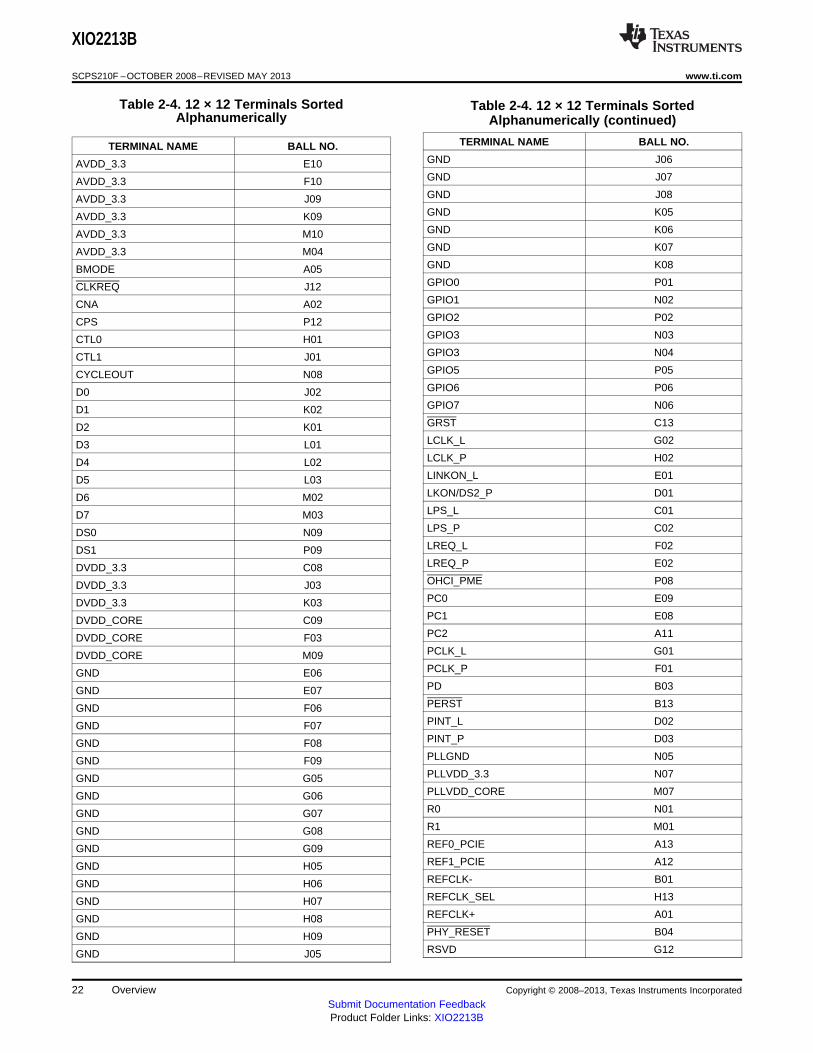
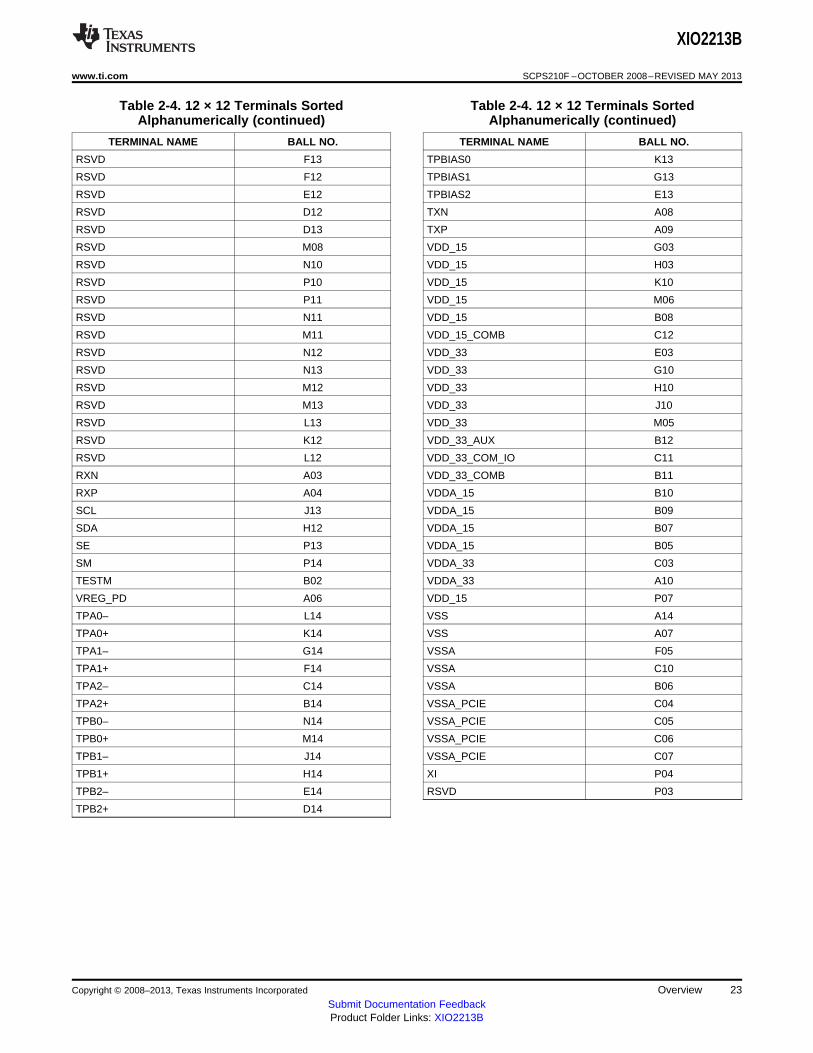
2-4 12 × 12 Terminals Sorted Alphanumerically .................................................................................. 22
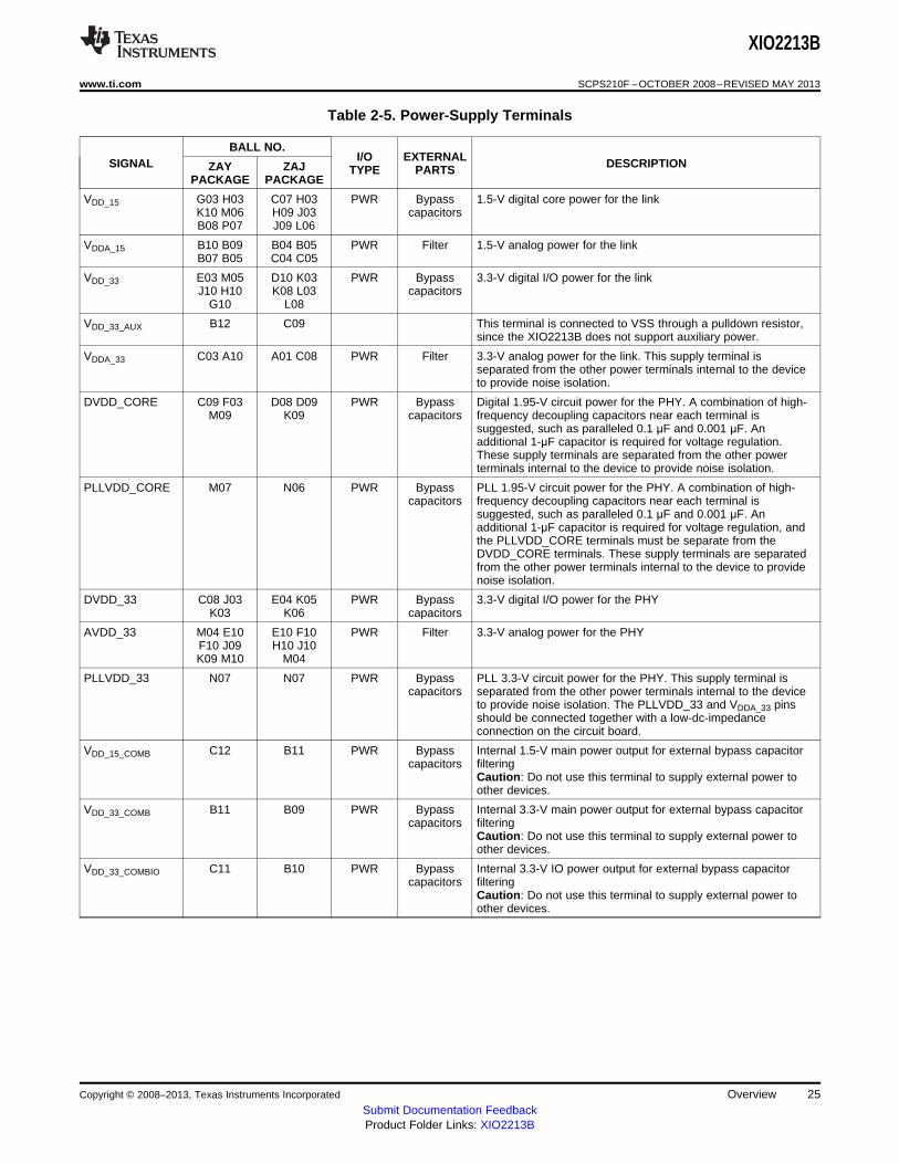
2-5 Power-Supply Terminals ........................................................................................................ 25
2-6 Ground Terminals ................................................................................................................ 26
2-7 PCIe Terminals ................................................................................................................... 26
2-8 Clock Terminals .................................................................................................................. 26
2-9 1394 Terminals ................................................................................................................... 27
2-10 Reserved Terminals.............................................................................................................. 29
2-11 Miscellaneous Terminals ........................................................................................................ 29
3-1 XIO2213B Reset Options ....................................................................................................... 34
3-2 Initial Flow Control Credit Advertisements .................................................................................... 35
3-3 Messages Supported by Bridge ................................................................................................ 36
3-4 EEPROM Register Loading Map............................................................................................... 41
3-5 Registers Used To Program Serial-Bus Devices............................................................................. 43
3-6 Clocking In Low Power States.................................................................................................. 44
3-7 1394b OHCI Configuration Register Map ..................................................................................... 46
3-8 1394 OHCI Memory Command Options ...................................................................................... 47
4-1 Classic PCI Configuration Register Map ...................................................................................... 48
4-2 Command Register Description ............................................................................................... 50
4-3 Status Register Description .................................................................................................... 51
4-4 Class Code and Revision ID Register Description .......................................................................... 52
4-5 Device Control Base Address Register Description ........................................................................ 53
4-6 Device Control Base Address Register Description ........................................................................ 54
4-7 I/O Base Register Description ................................................................................................. 55
4-8 I/O Limit Register Description .................................................................................................. 56
4-9 Secondary Status Register Description ...................................................................................... 57
4-10 Memory Base Register Description ........................................................................................... 58
4-11 Memory Limit Register Description ............................................................................................ 58
4-12 Prefetchable Memory Base Register Description ........................................................................... 59
4-13 Prefetchable Memory Limit Register Description ............................................................................ 59
4-14 Prefetchable Base Upper 32 Bits Register Description .................................................................... 60
4-15 Prefetchable Limit Upper 32 Bits Register Description ..................................................................... 60
4-16 I/O Base Upper 16 Bits Register Description ................................................................................ 61
4-17 I/O Limit Upper 16 Bits Register Description ................................................................................ 61
4-18 Bridge Control Register Description ........................................................................................... 63
4-19 Power Management Capabilities Register Description ..................................................................... 66
4-20 Power Management Control/Status Register Description .................................................................. 67
4-21 PM Bridge Support Extension Register Description ........................................................................ 68
4-22 MSI Message Control Register Description .................................................................................. 69
4-23 MSI Message Lower Address Register Description ........................................................................ 70
4-24 MSI Message Data Register Description ..................................................................................... 71
4-25 PCI Express Capabilities Register Description .............................................................................. 73
4-26 Device Capabilities Register Description ..................................................................................... 74
4-27 Device Control Register Description .......................................................................................... 75
4-28 Device Status Register Description ........................................................................................... 76
8 List of Tables Copyright © 2008–2013, Texas Instruments Incorporated
XIO2213B
www.ti.com SCPS210F –OCTOBER 2008–REVISED MAY 2013
4-29 Link Capabilities Register Description ........................................................................................ 77
4-30 Link Control Register Description ............................................................................................. 78
4-31 Link Status Register Description .............................................................................................. 79
4-32 Serial-Bus Slave Address Register Descriptions ............................................................................ 80
4-33 Serial-Bus Control and Status Register Description ........................................................................ 81
4-34 GPIO Control Register Description ............................................................................................ 82
4-35 GPIO Data Register Description ............................................................................................... 83
4-36 Control and Diagnostic Register 0 Description .............................................................................. 84
4-37 Control and Diagnostic Register 1 Description .............................................................................. 86
4-38 Control and Diagnostic Register 2 Description .............................................................................. 87
4-39 Subsystem Access Register Description ..................................................................................... 88
4-40 General Control Register Description ......................................................................................... 89
4-41 Arbiter Control Register Description .......................................................................................... 92
4-42 Arbiter Request Mask Register Description .................................................................................. 93
4-43 Arbiter Time-Out Status Register Description ............................................................................... 94
5-1 PCIe Extended Configuration Register Map.................................................................................. 96
5-2 Uncorrectable Error Status Register Description ............................................................................ 97
5-3 Uncorrectable Error Mask Register Description ............................................................................. 98
5-4 Uncorrectable Error Severity Register Description .......................................................................... 99
5-5 Correctable Error Status Register Description ............................................................................. 101
5-6 Correctable Error Mask Register Description .............................................................................. 102
5-7 Advanced Error Capabilities and Control Register Description .......................................................... 103
5-8 Secondary Uncorrectable Error Status Register Description ............................................................. 104
5-9 Secondary Uncorrectable Error Mask Register Description .............................................................. 105
5-10 Secondary Uncorrectable Error Severity Register Description .......................................................... 106
5-11 Secondary Error Capabilities and Control Register Description ......................................................... 107
5-12 Secondary Header Log Register Description .............................................................................. 108
6-1 Device Control Memory Window Register Map............................................................................. 109
6-2 GPIO Control Register Description .......................................................................................... 110
6-3 GPIO Data Register Description ............................................................................................. 111
6-4 Serial-Bus Slave Address Register Descriptions .......................................................................... 112
6-5 Serial-Bus Control and Status Register Description ....................................................................... 113
7-1 1394 OHCI Configuration Register Map ..................................................................................... 114
7-2 Command Register Description .............................................................................................. 116
7-3 Status Register Description ................................................................................................... 117
7-4 Class Code and Revision ID Registers Description ....................................................................... 118
7-5 Latency Timer and Class Cache Line Size Registers Description ...................................................... 118
7-6 Header Type and BIST Registers Description ............................................................................. 119
7-7 OHCI Base Address Register Description .................................................................................. 119
7-8 TI Base Address Register Description ...................................................................................... 120
7-9 Subsystem Vendor ID and Subsystem ID Registers Description ........................................................ 121
7-10 Interrupt Line and Interrupt Pin Registers Description .................................................................... 122
7-11 Minimum Grant and Minimum Latency Registers Description ........................................................... 123
7-12 OHCI Control Register Description .......................................................................................... 123
7-13 Capability ID and Next Item Pointer Registers Description ............................................................... 124
7-14 Power Management Capabilities Register Description ................................................................... 124
7-15 Power Management Control and Status Register Description ........................................................... 125
7-16 Power Management Extension Registers Description .................................................................... 125
Copyright © 2008–2013, Texas Instruments Incorporated List of Tables 9
XIO2213B
SCPS210F –OCTOBER 2008–REVISED MAY 2013 www.ti.com
7-17 PCI Miscellaneous Configuration Register ................................................................................. 127
7-18 Link Enhancement Control Register Description .......................................................................... 129
7-19 Subsystem Access Register Description ................................................................................... 130
8-1 OHCI Register Map............................................................................................................. 131
8-2 OHCI Version Register Description .......................................................................................... 134
8-3 GUID ROM Register Description ............................................................................................ 135
8-4 Asynchronous Transmit Retries Register Description ..................................................................... 136
8-5 CSR Control Register Description ........................................................................................... 137
8-6 Configuration ROM Header Register Description .......................................................................... 138
8-7 Bus Options Register Description ............................................................................................ 139
8-8 Configuration ROM Mapping Register Description ........................................................................ 141
8-9 Posted Write Address Low Register Description .......................................................................... 141
8-10 Posted Write Address High Register Description .......................................................................... 142
8-11 Host Controller Control Register Description ............................................................................... 144
8-12 Self-ID Count Register Description .......................................................................................... 145
8-13 Isochronous Receive Channel Mask High Register Description ......................................................... 146
8-14 Isochronous Receive Channel Mask Low Register Description ......................................................... 148
8-15 Interrupt Event Register Description ......................................................................................... 149
8-16 Interrupt Mask Register Description ......................................................................................... 150
8-17 Isochronous Transmit Interrupt Event Register Description .............................................................. 152
8-18 Isochronous Receive Interrupt Event Register Description ............................................................... 153
8-19 Initial Bandwidth Available Register Description ........................................................................... 154
8-20 Initial Channels Available High Register Description ...................................................................... 155
8-21 Initial Channels Available Low Register Description ...................................................................... 155
8-22 Fairness Control Registre Description ...................................................................................... 156
8-23 Link Control Register Description ............................................................................................ 157
8-24 Node Identification Register Description .................................................................................... 158
8-25 PHY Control Register Description ........................................................................................... 159
8-26 Isochronous Cycle Timer Register Description ............................................................................ 160
8-27 Asynchronous Request Filter High Register Description ................................................................. 161
8-28 Asynchronous Request Filter Low Register Description .................................................................. 163
8-29 Physical Request Filter High Register Description ........................................................................ 164
8-30 Physical Request Filter Low Register Description ......................................................................... 166
8-31 Asynchronous Context Control Register Description ...................................................................... 167
8-32 Asynchronous Context Command Pointer Register Description ......................................................... 168
8-33 Isochronous Transmit Context Control Register Description ............................................................. 169
8-34 Isochronous Receive Context Control Register Description ............................................................. 171
8-35 Isochronous Receive Context Match Register Description ............................................................... 172
9-1 TI Extension Register Map .................................................................................................... 174
9-2 Isochronous Receive Digital Video Enhancement Registers Description .............................................. 175
9-3 Link Enhancement Control Registers Description ......................................................................... 176
9-4 Timestamp Offset Registers Description .................................................................................... 178
10-1 Base Register Description .................................................................................................... 181
10-2 Base Register Field Description .............................................................................................. 181
10-3 Page 0 (Port Status) Register Description .................................................................................. 183
10-4 Page 0 (Port Status) Register Field Description ........................................................................... 184
10-5 Page 1 (Vendor ID) Register Configuration ................................................................................ 185
10-6 Page 1 (Vendor ID) Register Field Descriptions ........................................................................... 186
10 List of Tables Copyright © 2008–2013, Texas Instruments Incorporated

XIO2213B
www.ti.com SCPS210F –OCTOBER 2008–REVISED MAY 2013
10-7 Page 7 (Vendor Dependent) Register Configuration ...................................................................... 187
10-8 Page 7 (Vendor Dependent) Register Field Descriptions ................................................................ 187
10-9 Power Class Register Description ........................................................................................... 187
Copyright © 2008–2013, Texas Instruments Incorporated List of Tables 11

XIO2213B
SCPS210F –OCTOBER 2008–REVISED MAY 2013 www.ti.com
XIO2213BPCI Express™ TO 1394b OHCI WITH 3-PORT PHY
Check for Samples: XIO2213B
1 Introduction
1.1 XIO2213B Features123
Ports at 100M Bit/s, 200M Bit/s, 400M Bit/s, and• Full ×1 PCI Express™ (PCIe) Throughput800M Bit/s• Fully Compliant With PCI Express Base
• Cable Ports Monitor Line Conditions for ActiveSpecification, Revision 1.1Connection to Remote Node• Utilizes 100-MHz Differential PCI Express
• Cable Power Presence MonitoringCommon Reference Clock or 125-MHz Single-Ended Reference Clock • EEPROM Configuration Support to Load Global
Unique ID for 1394 Fabric• Fully Supports Provisions of IEEE Std P1394b-2002 • Support for D1, D2, D3hot
• Fully Compliant With Provisions of IEEE Std • Active-State Link Power Management Saves1394-1995 for a High-Performance Serial Bus Power When Packet Activity on the PCIand IEEE Std 1394a-2000 Express Link Is Idle, Using Both L0s and L1
States• Fully Compliant With 1394 Open HostController Interface (OHCI) Specification, • Eight 3.3-V Multifunction General-Purpose I/ORevision 1.1 and Revision 1.2 Draft (GPIO) Terminals
• Three IEEE Std 1394b Fully Compliant Cable
1
Please be aware that an important notice concerning availability, standard warranty, and use in critical applications ofTexas Instruments semiconductor products and disclaimers thereto appears at the end of this data sheet.
2OHCI-Lynx is a trademark of Texas Instruments.3PCI Express is a trademark of PCI-SIG.
PRODUCTION DATA information is current as of publication date. Products conform toCopyright © 2008–2013, Texas Instruments Incorporatedspecifications per the terms of the Texas Instruments standard warranty. Productionprocessing does not necessarily include testing of all parameters.

XIO2213B
www.ti.com SCPS210F –OCTOBER 2008–REVISED MAY 2013
2 Overview
The Texas Instruments XIO2213B is a single-function PCI Express™ (PCIe) to PCI local bus translationbridge, where the PCI bus interface is internally connected to a 1394b open host controller/link-layercontroller with a 3-port 1394b physical layer (PHY). When the XIO2213B is properly configured, thissolution provides full PCIe and 1394b functionality and performance.
The TI XIO2213B is a PCIe to PCI translation bridge, where the PCI bus interface is internally connectedto a 1394b open host controller/link-layer controller with a 3-port 1394b PHY. The PCIe to PCI translationbridge is fully compatible with the PCI Express to PCI/PCI-X Bridge Specification, Revision 1.0. Also, thebridge supports the standard PCI-to-PCI bridge programming model. The 1394b OHCI controller functionis fully compatible with IEEE Std 1394b and the latest 1394 Open Host Controller Interface (OHCI)Specification.
The XIO2213B simultaneously supports up to four posted write transactions, four nonposted transactions,and four completion transactions pending in each direction at any time. Each posted write data queue andcompletion data queue can store up to 8K bytes of data. The nonposted data queues can store up to 128bytes of data.
The PCIe interface supports a ×1 link operating at full 250 Mbit/s packet throughput in each directionsimultaneously. Also, the bridge supports the advanced error reporting capability including ECRC asdefined in the PCI Express Base Specification, Revision 1.1. Supplemental firmware or software isrequired to fully utilize both of these features.
Robust pipeline architecture is implemented to minimize system latency. If parity errors are detected,packet poisoning is supported for both upstream and downstream operations.
PCIe power management (PM) features include active-state link PM, PME mechanisms, and allconventional PCI D states. If the active-state link PM is enabled, the link automatically saves power whenidle using the L0s and L1 states. PM active-state NAK, PM PME, and PME-to-ACK messages aresupported. The bridge is compliant with the latest PCI Bus Power Management Specification and providesseveral low-power modes, which enable the host power system to further reduce power consumption
Eight general-purpose inputs and outputs (GPIOs), configured through accesses to the PCIe configurationspace, allow for further system control and customization.
Deep FIFOs are provided to buffer 1394 data and accommodate large host bus latencies. The deviceprovides physical write posting and a highly tuned physical data path for SBP-2 performance. The deviceis capable of transferring data between the PCIe bus and the 1394 bus at 100M bit/s, 200M bit/s, 400Mbit/s, and 800M bit/s. The device provides three 1394 ports that have separate cable bias (TPBIAS).
As required by the 1394 Open Host Controller Interface (OHCI) Specification, internal control registers arememory mapped and nonprefetchable. This configuration header is accessed through configuration cyclesspecified by PCIe, and it provides plug-and-play (PnP) compatibility.
The PHY provides the digital and analog transceiver functions needed to implement a 3-port node in acable-based 1394 network. Each cable port incorporates two differential line transceivers. Thetransceivers include circuitry to monitor the line conditions as needed for determining connection status,for initialization and arbitration, and for packet reception and transmission. An optional external 2-wireserial EEPROM interface is provided to load the global unique ID for the 1394 fabric.
The XIO2213B requires an external 98.304-MHz crystal oscillator to generate a reference clock. Theexternal clock drives an internal phase-locked loop (PLL), which generates the required reference signal.This reference signal provides the clock signals that control transmission of the outbound encodedinformation. The power-down (PD) function, when enabled by asserting the PD terminal high, stopsoperation of the PLL. Data bits to be transmitted through the cable ports are latched internally, combinedserially, encoded, and transmitted at 98.304, 196.608, 393.216, 491.52, or 983.04 Mbit/s (referred to asS100, S200, S400, S400B, or S800 speed, respectively) as the outbound information stream.
Copyright © 2008–2013, Texas Instruments Incorporated Overview 13Submit Documentation FeedbackProduct Folder Links: XIO2213B
XIO2213B
SCPS210F –OCTOBER 2008–REVISED MAY 2013 www.ti.com
To ensure that the XIO2213B conforms to IEEE Std 1394b-2002, the BMODE terminal must be asserted.The BMODE terminal does not select the cable-interface mode of operation. BMODE selects the internalPHY-section/LLC-section interface mode of operation and affects the arbitration modes on the cable.BMODE must be pulled high during normal operation.
Three package terminals are used as inputs to set the default value for three configuration status bits inthe self-ID packet. They can be pulled high through a 1-kΩ resistor or hardwired low as a function of theequipment design. The PC0, PC1, and PC2 terminals indicate the default power class status for the node(the need for power from the cable or the ability to supply power to the cable). The contender bit in thePHY register set indicates that the node is a contender either for the isochronous resource manager (IRM)or for the bus manager (BM). On the XIO2213B, this bit can only be set by a write to the PHY register set.If a node is to be a contender for IRM or BM, the node software must set this bit in the PHY register set.
2.1 Related Documents• PCI Express™ to PCI/PCI-X Bridge Specification, Revision 1.0• PCI Express™ Base Specification, Revision 1.1• PCI Express™ Card Electromechanical Specification, Revision 1.1• PCI Local Bus Specification, Revision 2.3 and Revision 3.0• PCI-to-PCI Bridge Architecture Specification, Revision 1.1• PCI Bus Power-Management Interface Specification, Revision 1.1 and Revision 1.2• 1394 Open Host Controller Interface (OHCI) Specification, Release 1.2• High-Performance Serial Bus, IEEE Std 1394-1995• High-Performance Serial Bus, Amendment 1, IEEE Std 1394a-2000• High-Performance Serial Bus, Amendment 2, IEEE Std 1394b-2002• Express Card Standard, Release 1.0 and Release 1.1• PCI Express™ Jitter and BER white paper• PCI Mobile Design Guide, Revision 1.1
14 Overview Copyright © 2008–2013, Texas Instruments Incorporated
Submit Documentation FeedbackProduct Folder Links: XIO2213B
XIO2213B
www.ti.com SCPS210F –OCTOBER 2008–REVISED MAY 2013
2.2 Documents Conventions
Throughout this data manual, several conventions are used to convey information. These conventions are:• To identify a binary number or field, a lower-case b follows the numbers. For example, 000b is a 3-bit
binary field.• To identify a hexadecimal number or field, a lower-case h follows the numbers. For example, 8AFh is a
12-bit hexadecimal field.• All other numbers that appear in this document that do not have either a b or h following the number
are assumed to be decimal format.• If the signal or terminal name has a bar above the name (for example, GRST), this indicates the logical
NOT function. When asserted, this signal is a logic low, 0, or 0b.• Differential signal names end with P, N, +, or – designators. The P or + designators signify the positive
signal associated with the differential pair. The N or – designators signify the negative signalassociated with the differential pair.
• RSVD indicates that the referenced item is reserved.• In Sections 4 through 6, the configuration space for the bridge is defined. For each register bit, the
software access method is identified in an access column. The legend for this access column includesthe following entries:– R: Read access by software– U: Updates by the bridge internal hardware– W: Write access by software– C: Clear an asserted bit with a write back of 1b by software. Write of zero to the field has no effect.– S: The field may be set by a write of one. Write of zero to the field has no effect.– NA: Not accessible or not applicable
• The XIO2213B consists of a PCIe to PCI translation bridge, where the secondary PCI bus is internallyconnected to a 1394b OHCI with a 3-port PHY. When describing functionality that is specific to thePCIe to PCI translation bridge, the term bridge is used to reduce text. The term 1394b OHCI is used toreduce text when describing the 1394b OHCI with 3-port PHY function.
• LLC refers to the 1394 link layer controller.
2.3 Ordering InformationPACKAGE VOLTAGE ORDERABLE PART NUMBER
XIO2213BZAY167-terminal (Lead-Free) PBGA – ZAY 3.3-V and 1.5-V power terminals
XIO2213BIZAY
168-terminal (Lead-Free) BGA – ZAJ 3.3-V and 1.5-V power terminals XIO2213BZAJ
Copyright © 2008–2013, Texas Instruments Incorporated Overview 15Submit Documentation FeedbackProduct Folder Links: XIO2213B
XIO2213B
SCPS210F –OCTOBER 2008–REVISED MAY 2013 www.ti.com
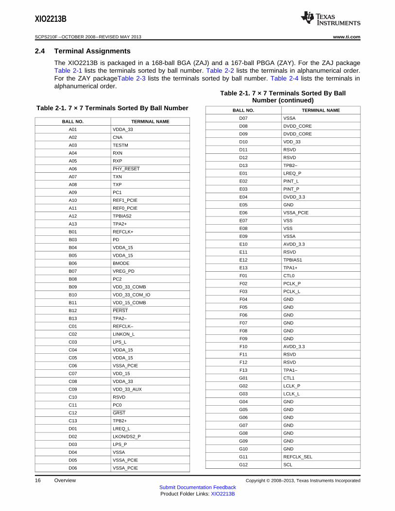
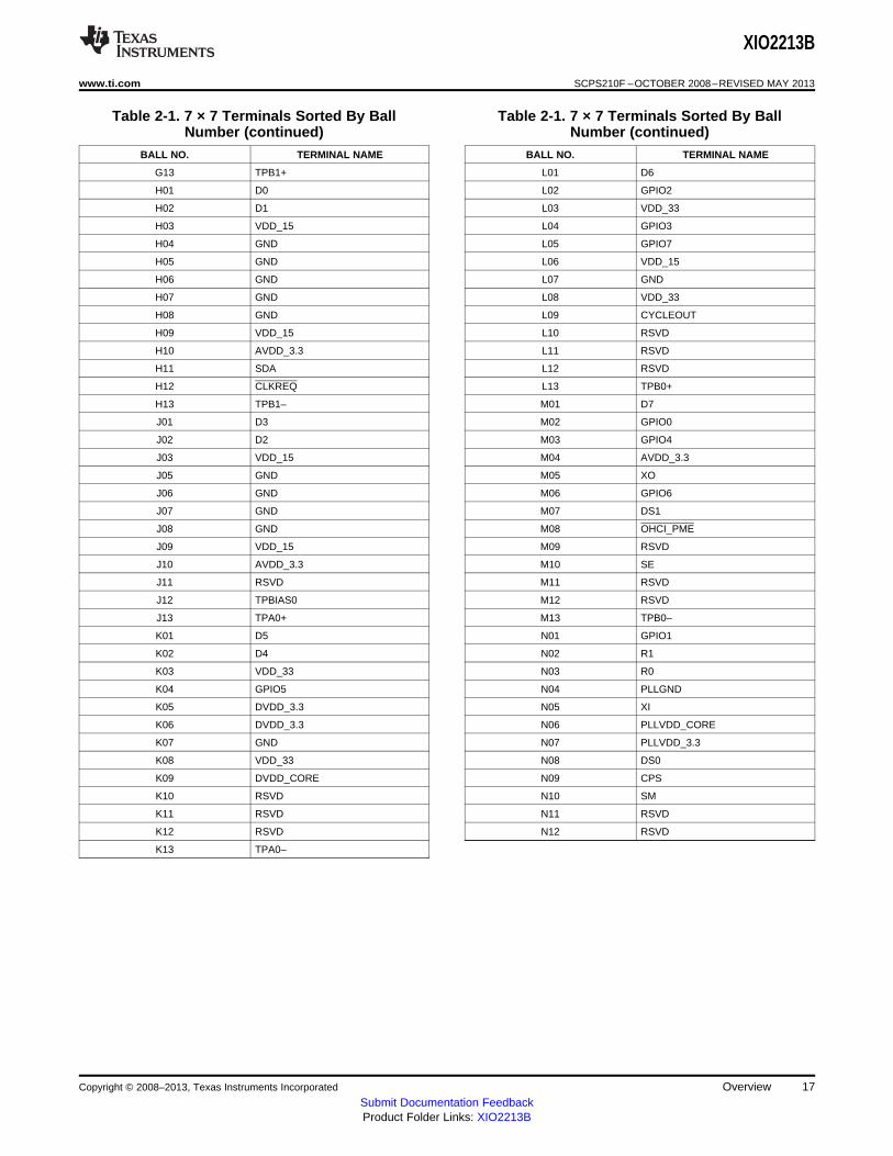
2.4 Terminal Assignments
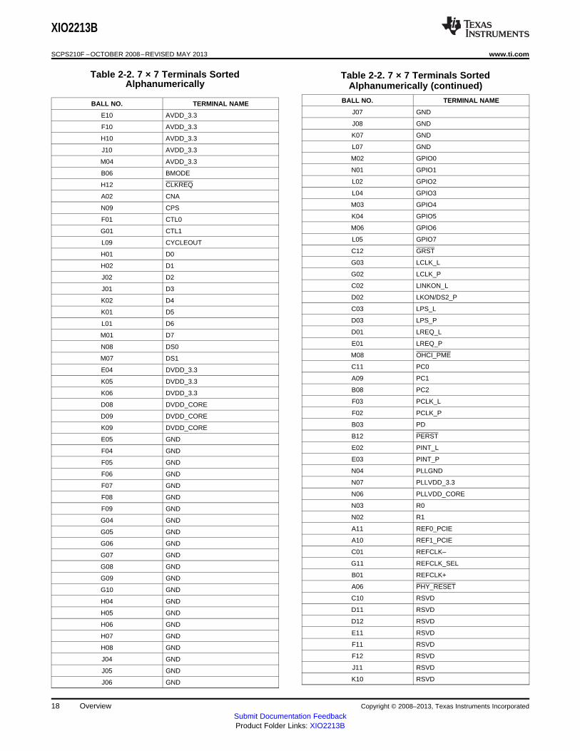
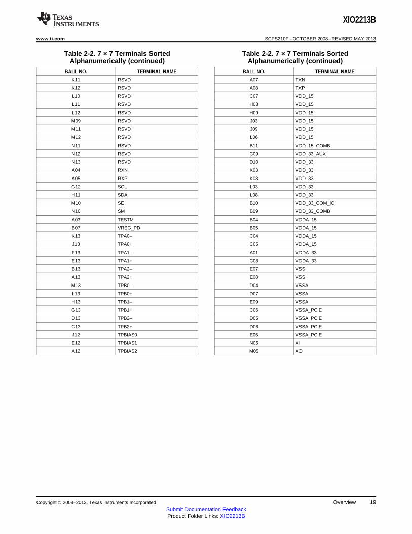
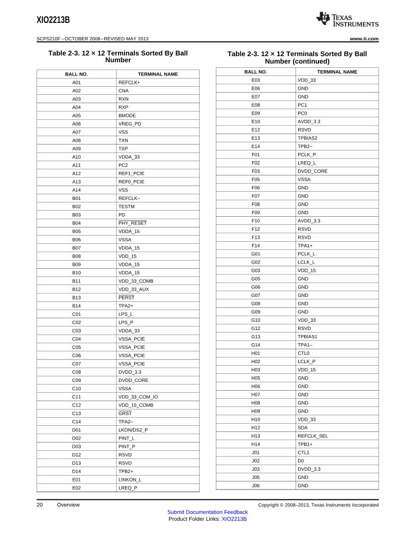
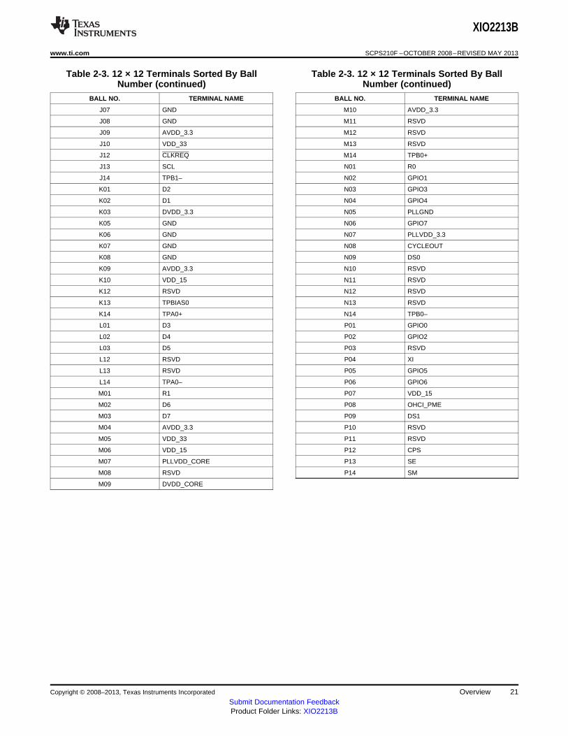
The XIO2213B is packaged in a 168-ball BGA (ZAJ) and a 167-ball PBGA (ZAY). For the ZAJ packageTable 2-1 lists the terminals sorted by ball number. Table 2-2 lists the terminals in alphanumerical order.For the ZAY packageTable 2-3 lists the terminals sorted by ball number. Table 2-4 lists the terminals inalphanumerical order.
Table 2-1. 7 × 7 Terminals Sorted By BallNumber (continued)
Table 2-1. 7 × 7 Terminals Sorted By Ball Number BALL NO. TERMINAL NAME
D07 VSSABALL NO. TERMINAL NAME
D08 DVDD_COREA01 VDDA_33
D09 DVDD_COREA02 CNA
D10 VDD_33A03 TESTM
D11 RSVDA04 RXN
D12 RSVDA05 RXP
D13 TPB2–A06 PHY_RESET
E01 LREQ_PA07 TXN
E02 PINT_LA08 TXP
E03 PINT_PA09 PC1
E04 DVDD_3.3A10 REF1_PCIE
E05 GNDA11 REF0_PCIE
E06 VSSA_PCIEA12 TPBIAS2
E07 VSSA13 TPA2+
E08 VSSB01 REFCLK+
E09 VSSAB03 PD
E10 AVDD_3.3B04 VDDA_15
E11 RSVDB05 VDDA_15
E12 TPBIAS1B06 BMODE
E13 TPA1+B07 VREG_PD
F01 CTL0B08 PC2
F02 PCLK_PB09 VDD_33_COMB
F03 PCLK_LB10 VDD_33_COM_IO
F04 GNDB11 VDD_15_COMB
F05 GNDB12 PERST
F06 GNDB13 TPA2–
F07 GNDC01 REFCLK–
F08 GNDC02 LINKON_L
F09 GNDC03 LPS_L
F10 AVDD_3.3C04 VDDA_15
F11 RSVDC05 VDDA_15
F12 RSVDC06 VSSA_PCIE
F13 TPA1–C07 VDD_15
G01 CTL1C08 VDDA_33
G02 LCLK_PC09 VDD_33_AUX
G03 LCLK_LC10 RSVD
G04 GNDC11 PC0
G05 GNDC12 GRST
G06 GNDC13 TPB2+
G07 GNDD01 LREQ_L
G08 GNDD02 LKON/DS2_P
G09 GNDD03 LPS_P
G10 GNDD04 VSSA
G11 REFCLK_SELD05 VSSA_PCIE
G12 SCLD06 VSSA_PCIE
16 Overview Copyright © 2008–2013, Texas Instruments Incorporated
Submit Documentation FeedbackProduct Folder Links: XIO2213B
XIO2213B
www.ti.com SCPS210F –OCTOBER 2008–REVISED MAY 2013
Table 2-1. 7 × 7 Terminals Sorted By Ball Table 2-1. 7 × 7 Terminals Sorted By BallNumber (continued) Number (continued)
BALL NO. TERMINAL NAME BALL NO. TERMINAL NAME
G13 TPB1+ L01 D6
H01 D0 L02 GPIO2
H02 D1 L03 VDD_33
H03 VDD_15 L04 GPIO3
H04 GND L05 GPIO7
H05 GND L06 VDD_15
H06 GND L07 GND
H07 GND L08 VDD_33
H08 GND L09 CYCLEOUT
H09 VDD_15 L10 RSVD
H10 AVDD_3.3 L11 RSVD
H11 SDA L12 RSVD
H12 CLKREQ L13 TPB0+
H13 TPB1– M01 D7
J01 D3 M02 GPIO0
J02 D2 M03 GPIO4
J03 VDD_15 M04 AVDD_3.3
J05 GND M05 XO
J06 GND M06 GPIO6
J07 GND M07 DS1
J08 GND M08 OHCI_PME
J09 VDD_15 M09 RSVD
J10 AVDD_3.3 M10 SE
J11 RSVD M11 RSVD
J12 TPBIAS0 M12 RSVD
J13 TPA0+ M13 TPB0–
K01 D5 N01 GPIO1
K02 D4 N02 R1
K03 VDD_33 N03 R0
K04 GPIO5 N04 PLLGND
K05 DVDD_3.3 N05 XI
K06 DVDD_3.3 N06 PLLVDD_CORE
K07 GND N07 PLLVDD_3.3
K08 VDD_33 N08 DS0
K09 DVDD_CORE N09 CPS
K10 RSVD N10 SM
K11 RSVD N11 RSVD
K12 RSVD N12 RSVD
K13 TPA0–
Copyright © 2008–2013, Texas Instruments Incorporated Overview 17Submit Documentation FeedbackProduct Folder Links: XIO2213B
XIO2213B
SCPS210F –OCTOBER 2008–REVISED MAY 2013 www.ti.com
Table 2-2. 7 × 7 Terminals Sorted Table 2-2. 7 × 7 Terminals SortedAlphanumerically Alphanumerically (continued)
BALL NO. TERMINAL NAMEBALL NO. TERMINAL NAMEJ07 GNDE10 AVDD_3.3J08 GNDF10 AVDD_3.3K07 GNDH10 AVDD_3.3L07 GNDJ10 AVDD_3.3M02 GPIO0M04 AVDD_3.3N01 GPIO1B06 BMODEL02 GPIO2H12 CLKREQL04 GPIO3A02 CNAM03 GPIO4N09 CPSK04 GPIO5F01 CTL0M06 GPIO6G01 CTL1L05 GPIO7L09 CYCLEOUTC12 GRSTH01 D0G03 LCLK_LH02 D1G02 LCLK_PJ02 D2C02 LINKON_LJ01 D3D02 LKON/DS2_PK02 D4C03 LPS_LK01 D5D03 LPS_PL01 D6D01 LREQ_LM01 D7E01 LREQ_PN08 DS0M08 OHCI_PMEM07 DS1C11 PC0E04 DVDD_3.3A09 PC1K05 DVDD_3.3B08 PC2K06 DVDD_3.3F03 PCLK_LD08 DVDD_COREF02 PCLK_PD09 DVDD_COREB03 PDK09 DVDD_COREB12 PERSTE05 GNDE02 PINT_LF04 GNDE03 PINT_PF05 GNDN04 PLLGNDF06 GNDN07 PLLVDD_3.3F07 GNDN06 PLLVDD_COREF08 GNDN03 R0F09 GNDN02 R1G04 GNDA11 REF0_PCIEG05 GNDA10 REF1_PCIEG06 GNDC01 REFCLK–G07 GNDG11 REFCLK_SELG08 GNDB01 REFCLK+G09 GNDA06 PHY_RESETG10 GNDC10 RSVDH04 GNDD11 RSVDH05 GNDD12 RSVDH06 GNDE11 RSVDH07 GNDF11 RSVDH08 GNDF12 RSVDJ04 GNDJ11 RSVDJ05 GNDK10 RSVDJ06 GND
18 Overview Copyright © 2008–2013, Texas Instruments Incorporated
Submit Documentation FeedbackProduct Folder Links: XIO2213B
XIO2213B
www.ti.com SCPS210F –OCTOBER 2008–REVISED MAY 2013
Table 2-2. 7 × 7 Terminals Sorted Table 2-2. 7 × 7 Terminals SortedAlphanumerically (continued) Alphanumerically (continued)
BALL NO. TERMINAL NAME BALL NO. TERMINAL NAME
K11 RSVD A07 TXN
K12 RSVD A08 TXP
L10 RSVD C07 VDD_15
L11 RSVD H03 VDD_15
L12 RSVD H09 VDD_15
M09 RSVD J03 VDD_15
M11 RSVD J09 VDD_15
M12 RSVD L06 VDD_15
N11 RSVD B11 VDD_15_COMB
N12 RSVD C09 VDD_33_AUX
N13 RSVD D10 VDD_33
A04 RXN K03 VDD_33
A05 RXP K08 VDD_33
G12 SCL L03 VDD_33
H11 SDA L08 VDD_33
M10 SE B10 VDD_33_COM_IO
N10 SM B09 VDD_33_COMB
A03 TESTM B04 VDDA_15
B07 VREG_PD B05 VDDA_15
K13 TPA0– C04 VDDA_15
J13 TPA0+ C05 VDDA_15
F13 TPA1– A01 VDDA_33
E13 TPA1+ C08 VDDA_33
B13 TPA2– E07 VSS
A13 TPA2+ E08 VSS
M13 TPB0– D04 VSSA
L13 TPB0+ D07 VSSA
H13 TPB1– E09 VSSA
G13 TPB1+ C06 VSSA_PCIE
D13 TPB2– D05 VSSA_PCIE
C13 TPB2+ D06 VSSA_PCIE
J12 TPBIAS0 E06 VSSA_PCIE
E12 TPBIAS1 N05 XI
A12 TPBIAS2 M05 XO
Copyright © 2008–2013, Texas Instruments Incorporated Overview 19Submit Documentation FeedbackProduct Folder Links: XIO2213B
XIO2213B
SCPS210F –OCTOBER 2008–REVISED MAY 2013 www.ti.com
Table 2-3. 12 × 12 Terminals Sorted By Ball Table 2-3. 12 × 12 Terminals Sorted By BallNumber Number (continued)
BALL NO. TERMINAL NAMEBALL NO. TERMINAL NAMEE03 VDD_33A01 REFCLK+E06 GNDA02 CNAE07 GNDA03 RXNE08 PC1A04 RXPE09 PC0A05 BMODEE10 AVDD_3.3A06 VREG_PDE12 RSVDA07 VSSE13 TPBIAS2A08 TXNE14 TPB2–A09 TXPF01 PCLK_PA10 VDDA_33F02 LREQ_LA11 PC2F03 DVDD_COREA12 REF1_PCIEF05 VSSAA13 REF0_PCIEF06 GNDA14 VSSF07 GNDB01 REFCLK–F08 GNDB02 TESTMF09 GNDB03 PDF10 AVDD_3.3B04 PHY_RESETF12 RSVDB05 VDDA_15F13 RSVDB06 VSSAF14 TPA1+B07 VDDA_15G01 PCLK_LB08 VDD_15G02 LCLK_LB09 VDDA_15G03 VDD_15B10 VDDA_15G05 GNDB11 VDD_33_COMBG06 GNDB12 VDD_33_AUXG07 GNDB13 PERSTG08 GNDB14 TPA2+G09 GNDC01 LPS_LG10 VDD_33C02 LPS_PG12 RSVDC03 VDDA_33G13 TPBIAS1C04 VSSA_PCIEG14 TPA1–C05 VSSA_PCIEH01 CTL0C06 VSSA_PCIEH02 LCLK_PC07 VSSA_PCIEH03 VDD_15C08 DVDD_3.3H05 GNDC09 DVDD_COREH06 GNDC10 VSSAH07 GNDC11 VDD_33_COM_IOH08 GNDC12 VDD_15_COMBH09 GNDC13 GRSTH10 VDD_33C14 TPA2–H12 SDAD01 LKON/DS2_PH13 REFCLK_SELD02 PINT_LH14 TPB1+D03 PINT_PJ01 CTL1D12 RSVDJ02 D0D13 RSVDJ03 DVDD_3.3D14 TPB2+J05 GNDE01 LINKON_LJ06 GNDE02 LREQ_P
20 Overview Copyright © 2008–2013, Texas Instruments Incorporated
Submit Documentation FeedbackProduct Folder Links: XIO2213B
XIO2213B
www.ti.com SCPS210F –OCTOBER 2008–REVISED MAY 2013
Table 2-3. 12 × 12 Terminals Sorted By Ball Table 2-3. 12 × 12 Terminals Sorted By BallNumber (continued) Number (continued)
BALL NO. TERMINAL NAME BALL NO. TERMINAL NAME
J07 GND M10 AVDD_3.3
J08 GND M11 RSVD
J09 AVDD_3.3 M12 RSVD
J10 VDD_33 M13 RSVD
J12 CLKREQ M14 TPB0+
J13 SCL N01 R0
J14 TPB1– N02 GPIO1
K01 D2 N03 GPIO3
K02 D1 N04 GPIO4
K03 DVDD_3.3 N05 PLLGND
K05 GND N06 GPIO7
K06 GND N07 PLLVDD_3.3
K07 GND N08 CYCLEOUT
K08 GND N09 DS0
K09 AVDD_3.3 N10 RSVD
K10 VDD_15 N11 RSVD
K12 RSVD N12 RSVD
K13 TPBIAS0 N13 RSVD
K14 TPA0+ N14 TPB0–
L01 D3 P01 GPIO0
L02 D4 P02 GPIO2
L03 D5 P03 RSVD
L12 RSVD P04 XI
L13 RSVD P05 GPIO5
L14 TPA0– P06 GPIO6
M01 R1 P07 VDD_15
M02 D6 P08 OHCI_PME
M03 D7 P09 DS1
M04 AVDD_3.3 P10 RSVD
M05 VDD_33 P11 RSVD
M06 VDD_15 P12 CPS
M07 PLLVDD_CORE P13 SE
M08 RSVD P14 SM
M09 DVDD_CORE
Copyright © 2008–2013, Texas Instruments Incorporated Overview 21Submit Documentation FeedbackProduct Folder Links: XIO2213B
XIO2213B
SCPS210F –OCTOBER 2008–REVISED MAY 2013 www.ti.com
Table 2-4. 12 × 12 Terminals Sorted Table 2-4. 12 × 12 Terminals SortedAlphanumerically Alphanumerically (continued)
TERMINAL NAME BALL NO.TERMINAL NAME BALL NO.GND J06AVDD_3.3 E10GND J07AVDD_3.3 F10GND J08AVDD_3.3 J09GND K05AVDD_3.3 K09GND K06AVDD_3.3 M10GND K07AVDD_3.3 M04GND K08BMODE A05GPIO0 P01CLKREQ J12GPIO1 N02CNA A02GPIO2 P02CPS P12GPIO3 N03CTL0 H01GPIO3 N04CTL1 J01GPIO5 P05CYCLEOUT N08GPIO6 P06D0 J02GPIO7 N06D1 K02GRST C13D2 K01LCLK_L G02D3 L01LCLK_P H02D4 L02LINKON_L E01D5 L03LKON/DS2_P D01D6 M02LPS_L C01D7 M03LPS_P C02DS0 N09LREQ_L F02DS1 P09LREQ_P E02DVDD_3.3 C08OHCI_PME P08DVDD_3.3 J03PC0 E09DVDD_3.3 K03PC1 E08DVDD_CORE C09PC2 A11DVDD_CORE F03PCLK_L G01DVDD_CORE M09PCLK_P F01GND E06PD B03GND E07PERST B13GND F06PINT_L D02GND F07PINT_P D03GND F08PLLGND N05GND F09PLLVDD_3.3 N07GND G05PLLVDD_CORE M07GND G06R0 N01GND G07R1 M01GND G08REF0_PCIE A13GND G09REF1_PCIE A12GND H05REFCLK- B01GND H06REFCLK_SEL H13GND H07REFCLK+ A01GND H08PHY_RESET B04GND H09RSVD G12GND J05
22 Overview Copyright © 2008–2013, Texas Instruments Incorporated
Submit Documentation FeedbackProduct Folder Links: XIO2213B
XIO2213B
www.ti.com SCPS210F –OCTOBER 2008–REVISED MAY 2013
Table 2-4. 12 × 12 Terminals Sorted Table 2-4. 12 × 12 Terminals SortedAlphanumerically (continued) Alphanumerically (continued)
TERMINAL NAME BALL NO. TERMINAL NAME BALL NO.
RSVD F13 TPBIAS0 K13
RSVD F12 TPBIAS1 G13
RSVD E12 TPBIAS2 E13
RSVD D12 TXN A08
RSVD D13 TXP A09
RSVD M08 VDD_15 G03
RSVD N10 VDD_15 H03
RSVD P10 VDD_15 K10
RSVD P11 VDD_15 M06
RSVD N11 VDD_15 B08
RSVD M11 VDD_15_COMB C12
RSVD N12 VDD_33 E03
RSVD N13 VDD_33 G10
RSVD M12 VDD_33 H10
RSVD M13 VDD_33 J10
RSVD L13 VDD_33 M05
RSVD K12 VDD_33_AUX B12
RSVD L12 VDD_33_COM_IO C11
RXN A03 VDD_33_COMB B11
RXP A04 VDDA_15 B10
SCL J13 VDDA_15 B09
SDA H12 VDDA_15 B07
SE P13 VDDA_15 B05
SM P14 VDDA_33 C03
TESTM B02 VDDA_33 A10
VREG_PD A06 VDD_15 P07
TPA0– L14 VSS A14
TPA0+ K14 VSS A07
TPA1– G14 VSSA F05
TPA1+ F14 VSSA C10
TPA2– C14 VSSA B06
TPA2+ B14 VSSA_PCIE C04
TPB0– N14 VSSA_PCIE C05
TPB0+ M14 VSSA_PCIE C06
TPB1– J14 VSSA_PCIE C07
TPB1+ H14 XI P04
TPB2– E14 RSVD P03
TPB2+ D14
Copyright © 2008–2013, Texas Instruments Incorporated Overview 23Submit Documentation FeedbackProduct Folder Links: XIO2213B
XIO2213B
SCPS210F –OCTOBER 2008–REVISED MAY 2013 www.ti.com
2.5 Terminal Descriptions
The following tables give a description of the terminals. These terminals are grouped in tables byfunctionality. Each table includes the terminal name, terminal number, I/O type, and terminal description.
The following list describes the different input/output cell types that appear in the terminal descriptiontables:• HS DIFF IN = High-speed differential input• HS DIFF OUT = High-speed differential output• LV CMOS = 3.3-V low-voltage CMOS input or output with 3.3-V clamp rail• BIAS = Input/output terminals that generate a bias voltage to determine a driver's operating current• Feedthrough = Terminals that connect directly to macros within the part and not through an input or
output cell• PWR = Power terminal• GND = Ground terminal
24 Overview Copyright © 2008–2013, Texas Instruments Incorporated
Submit Documentation FeedbackProduct Folder Links: XIO2213B
XIO2213B
www.ti.com SCPS210F –OCTOBER 2008–REVISED MAY 2013
Table 2-5. Power-Supply Terminals
BALL NO.I/O EXTERNALSIGNAL DESCRIPTIONZAY ZAJ TYPE PARTS
PACKAGE PACKAGE
VDD_15 G03 H03 C07 H03 PWR Bypass 1.5-V digital core power for the linkK10 M06 H09 J03 capacitorsB08 P07 J09 L06
VDDA_15 B10 B09 B04 B05 PWR Filter 1.5-V analog power for the linkB07 B05 C04 C05
VDD_33 E03 M05 D10 K03 PWR Bypass 3.3-V digital I/O power for the linkJ10 H10 K08 L03 capacitors
G10 L08
VDD_33_AUX B12 C09 This terminal is connected to VSS through a pulldown resistor,since the XIO2213B does not support auxiliary power.
VDDA_33 C03 A10 A01 C08 PWR Filter 3.3-V analog power for the link. This supply terminal isseparated from the other power terminals internal to the deviceto provide noise isolation.
DVDD_CORE C09 F03 D08 D09 PWR Bypass Digital 1.95-V circuit power for the PHY. A combination of high-M09 K09 capacitors frequency decoupling capacitors near each terminal is
suggested, such as paralleled 0.1 μF and 0.001 μF. Anadditional 1-μF capacitor is required for voltage regulation.These supply terminals are separated from the other powerterminals internal to the device to provide noise isolation.
PLLVDD_CORE M07 N06 PWR Bypass PLL 1.95-V circuit power for the PHY. A combination of high-capacitors frequency decoupling capacitors near each terminal is
suggested, such as paralleled 0.1 μF and 0.001 μF. Anadditional 1-μF capacitor is required for voltage regulation, andthe PLLVDD_CORE terminals must be separate from theDVDD_CORE terminals. These supply terminals are separatedfrom the other power terminals internal to the device to providenoise isolation.
DVDD_33 C08 J03 E04 K05 PWR Bypass 3.3-V digital I/O power for the PHYK03 K06 capacitors
AVDD_33 M04 E10 E10 F10 PWR Filter 3.3-V analog power for the PHYF10 J09 H10 J10K09 M10 M04
PLLVDD_33 N07 N07 PWR Bypass PLL 3.3-V circuit power for the PHY. This supply terminal iscapacitors separated from the other power terminals internal to the device
to provide noise isolation. The PLLVDD_33 and VDDA_33 pinsshould be connected together with a low-dc-impedanceconnection on the circuit board.
VDD_15_COMB C12 B11 PWR Bypass Internal 1.5-V main power output for external bypass capacitorcapacitors filtering
Caution: Do not use this terminal to supply external power toother devices.
VDD_33_COMB B11 B09 PWR Bypass Internal 3.3-V main power output for external bypass capacitorcapacitors filtering
Caution: Do not use this terminal to supply external power toother devices.
VDD_33_COMBIO C11 B10 PWR Bypass Internal 3.3-V IO power output for external bypass capacitorcapacitors filtering
Caution: Do not use this terminal to supply external power toother devices.
Copyright © 2008–2013, Texas Instruments Incorporated Overview 25Submit Documentation FeedbackProduct Folder Links: XIO2213B
XIO2213B
SCPS210F –OCTOBER 2008–REVISED MAY 2013 www.ti.com
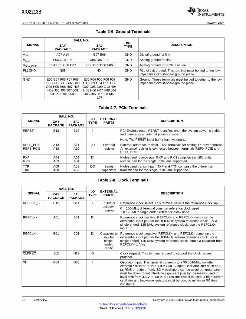
Table 2-6. Ground Terminals
BALL NO.I/OSIGNAL DESCRIPTIONZAY ZAJ TYPE
PACKAGE PACKAGE
VSS A07 A14 E07 E08 GND Digital ground for link
VSSA B06 C10 F05 D04 D07 E09 GND Analog ground for link
VSSA_PCIE C04 C05 C06 C07 C06 D05 D06 E06 GND Analog ground for PCIe function
PLLGND N05 N04 GND PLL circuit ground. This terminal must be tied to the low-impedance circuit-board ground plane.
GND E06 E07 F06 F07 F08 E05 F04 F05 F06 F07 GND Ground. These terminals must be tied together to the low-F09 G05 G06 G07 G08 F08 F09 G04 G05 G06 impedance circuit-board ground plane.G09 H05 H06 H07 H08 G07 G08 G09 G10 H04H09 J05 J06 J07 J08 H05 H06 H07 H08 J04
K05 K06 K07 K08 J05 J06 J07 J08 K07L07
Table 2-7. PCIe Terminals
BALL NO.I/O EXTERNALSIGNAL DESCRIPTIONZAY ZAJ TYPE PARTS
PACKAGE PACKAGE
PERST B13 B12 I PCI Express reset. PERST identifies when the system power is stableand generates an internal power-on reset.
Note: The PERST input buffer has hysteresis.
REF0_PCIE A13 A11 I/O External External reference resistor + and terminals for setting TX driver current.REF1_PCIE A12 A10 resistor An external resistor is connected between terminals REF0_PCIE and
REF1_PCIE.
RXP A04 A05 DI High-speed receive pair. RXP and RXN comprise the differentialRXN A03 A04 receive pair for the single PCIe lane supported.
TXP A09 A08 DO Series High-speed transmit pair. TXP and TXN comprise the differentialTXN A08 A07 capacitors transmit pair for the single PCIe lane supported.
Table 2-8. Clock Terminals
BALL NO.I/O EXTERNALSIGNAL DESCRIPTIONZAY ZAJ TYPE PARTS
PACKAGE PACKAGE
REFCLK_SEL H13 G11 I Pullup or Reference clock select. This terminal selects the reference clock input.pulldown 0 = 100-MHz differential common reference clock usedresistor 1 = 125-MHz single-ended reference clock used
REFCLK+ A01 B01 DI Reference clock positive. REFCLK+ and REFCLK– comprise thedifferential input pair for the 100-MHz system reference clock. For asingle-ended, 125-MHz system reference clock, use the REFCLK+input.
REFCLK– B01 C01 DI Capacitor to Reference clock negative. REFCLK+ and REFCLK– comprise theVSS for differential input pair for the 100-MHz system reference clock. For asingle- single-ended, 125-MHz system reference clock, attach a capacitor fromended REFCLK– to VSS.mode
CLKREQ J12 H12 O Clock request. This terminal is used to support the clock requestprotocol.
XI P04 N05 I Oscillator input. This terminal connects to a 98.304-MHz low-jitterexternal oscillator. XI is a 1.8-V CMOS input. Oscillator jitter must be 5-ps RMS or better. If only 3.3-V oscillators can be acquired, great caremust be taken to not introduce significant jitter by the means used tolevel shift from 3.3 V to 1.8 V. If a resistor divider is used, a high-currentoscillator and low-value resistors must be used to minimize RC timeconstants.
26 Overview Copyright © 2008–2013, Texas Instruments Incorporated
Submit Documentation FeedbackProduct Folder Links: XIO2213B
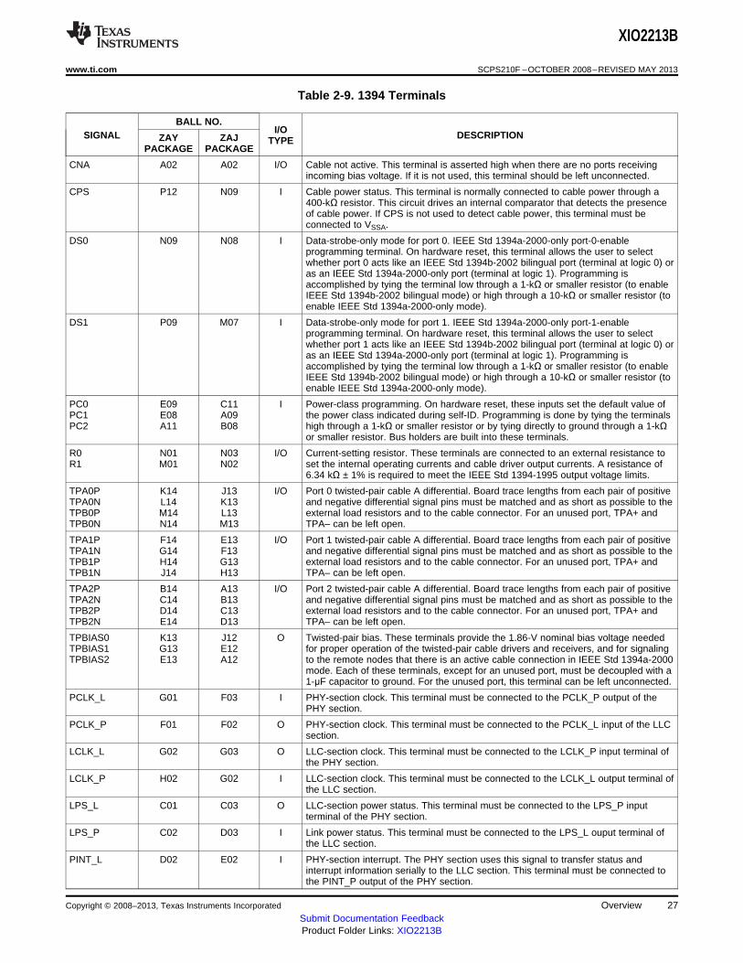
XIO2213B
www.ti.com SCPS210F –OCTOBER 2008–REVISED MAY 2013
Table 2-9. 1394 Terminals
BALL NO.I/OSIGNAL DESCRIPTIONZAY ZAJ TYPE
PACKAGE PACKAGE
CNA A02 A02 I/O Cable not active. This terminal is asserted high when there are no ports receivingincoming bias voltage. If it is not used, this terminal should be left unconnected.
CPS P12 N09 I Cable power status. This terminal is normally connected to cable power through a400-kΩ resistor. This circuit drives an internal comparator that detects the presenceof cable power. If CPS is not used to detect cable power, this terminal must beconnected to VSSA.
DS0 N09 N08 I Data-strobe-only mode for port 0. IEEE Std 1394a-2000-only port-0-enableprogramming terminal. On hardware reset, this terminal allows the user to selectwhether port 0 acts like an IEEE Std 1394b-2002 bilingual port (terminal at logic 0) oras an IEEE Std 1394a-2000-only port (terminal at logic 1). Programming isaccomplished by tying the terminal low through a 1-kΩ or smaller resistor (to enableIEEE Std 1394b-2002 bilingual mode) or high through a 10-kΩ or smaller resistor (toenable IEEE Std 1394a-2000-only mode).
DS1 P09 M07 I Data-strobe-only mode for port 1. IEEE Std 1394a-2000-only port-1-enableprogramming terminal. On hardware reset, this terminal allows the user to selectwhether port 1 acts like an IEEE Std 1394b-2002 bilingual port (terminal at logic 0) oras an IEEE Std 1394a-2000-only port (terminal at logic 1). Programming isaccomplished by tying the terminal low through a 1-kΩ or smaller resistor (to enableIEEE Std 1394b-2002 bilingual mode) or high through a 10-kΩ or smaller resistor (toenable IEEE Std 1394a-2000-only mode).
PC0 E09 C11 I Power-class programming. On hardware reset, these inputs set the default value ofPC1 E08 A09 the power class indicated during self-ID. Programming is done by tying the terminalsPC2 A11 B08 high through a 1-kΩ or smaller resistor or by tying directly to ground through a 1-kΩ
or smaller resistor. Bus holders are built into these terminals.
R0 N01 N03 I/O Current-setting resistor. These terminals are connected to an external resistance toR1 M01 N02 set the internal operating currents and cable driver output currents. A resistance of
6.34 kΩ ± 1% is required to meet the IEEE Std 1394-1995 output voltage limits.
TPA0P K14 J13 I/O Port 0 twisted-pair cable A differential. Board trace lengths from each pair of positiveTPA0N L14 K13 and negative differential signal pins must be matched and as short as possible to theTPB0P M14 L13 external load resistors and to the cable connector. For an unused port, TPA+ andTPB0N N14 M13 TPA– can be left open.
TPA1P F14 E13 I/O Port 1 twisted-pair cable A differential. Board trace lengths from each pair of positiveTPA1N G14 F13 and negative differential signal pins must be matched and as short as possible to theTPB1P H14 G13 external load resistors and to the cable connector. For an unused port, TPA+ andTPB1N J14 H13 TPA– can be left open.
TPA2P B14 A13 I/O Port 2 twisted-pair cable A differential. Board trace lengths from each pair of positiveTPA2N C14 B13 and negative differential signal pins must be matched and as short as possible to theTPB2P D14 C13 external load resistors and to the cable connector. For an unused port, TPA+ andTPB2N E14 D13 TPA– can be left open.
TPBIAS0 K13 J12 O Twisted-pair bias. These terminals provide the 1.86-V nominal bias voltage neededTPBIAS1 G13 E12 for proper operation of the twisted-pair cable drivers and receivers, and for signalingTPBIAS2 E13 A12 to the remote nodes that there is an active cable connection in IEEE Std 1394a-2000
mode. Each of these terminals, except for an unused port, must be decoupled with a1-μF capacitor to ground. For the unused port, this terminal can be left unconnected.
PCLK_L G01 F03 I PHY-section clock. This terminal must be connected to the PCLK_P output of thePHY section.
PCLK_P F01 F02 O PHY-section clock. This terminal must be connected to the PCLK_L input of the LLCsection.
LCLK_L G02 G03 O LLC-section clock. This terminal must be connected to the LCLK_P input terminal ofthe PHY section.
LCLK_P H02 G02 I LLC-section clock. This terminal must be connected to the LCLK_L output terminal ofthe LLC section.
LPS_L C01 C03 O LLC-section power status. This terminal must be connected to the LPS_P inputterminal of the PHY section.
LPS_P C02 D03 I Link power status. This terminal must be connected to the LPS_L ouput terminal ofthe LLC section.
PINT_L D02 E02 I PHY-section interrupt. The PHY section uses this signal to transfer status andinterrupt information serially to the LLC section. This terminal must be connected tothe PINT_P output of the PHY section.
Copyright © 2008–2013, Texas Instruments Incorporated Overview 27Submit Documentation FeedbackProduct Folder Links: XIO2213B
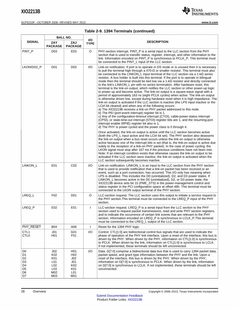
XIO2213B
SCPS210F –OCTOBER 2008–REVISED MAY 2013 www.ti.com
Table 2-9. 1394 Terminals (continued)
BALL NO.I/OSIGNAL DESCRIPTIONZAY ZAJ TYPE
PACKAGE PACKAGE
PINT_P D03 E03 O PHY-section interrupt. PINT_P is a serial input to the LLC section from the PHYsection that is used to transfer status, register, interrupt, and other information to thelink. Information encoded on PINT_P is synchronous to PCLK_P. This terminal mustbe connected to the PINT_L input of the LLC section.
LKON/DS2_P D01 D02 I/O Link-on notification. If port is to operate in DS mode or is unused then it is necessaryto pull the terminal high through a 470-Ω or smaller resistor. This terminal must alsobe connected to the LINKON_L input terminal of the LLC section via a 1-kΩ seriesresistor. A bus holder is built into this terminal. If the port is to operate in bilingualmode then the terminal should be tied low via a 1-kΩ resistor and directly connectedto the link's LINKON_L pin with no series termination. After hardware reset, thisterminal is the link-on output, which notifies the LLC section or other power-up logicto power up and become active. The link-on output is a square-wave signal with aperiod of approximately 163 ns (eight PCLK cycles) when active. The link-on outputis otherwise driven low, except during hardware reset when it is high impedance. Thelink-on output is activated if the LLC section is inactive (the LPS input inactive or theLCtrl bit cleared) and when any of the following occurs:a) The XIO2213B receives a link-on PHY packet addressed to this node.b) The PEI (port-event interrupt) register bit is 1.c) Any of the configuration-timeout interrupt (CTOI), cable-power-status interrupt(CPSI), or state-time-out interrupt (STOI) register bits are 1, and the resuming-portinterrupt enable (RPIE) register bit also is 1.d) The PHY is power cycled and the power class is 0 through 4.
Once activated, the link-on output is active until the LLC section becomes active(both the LPS_L input active and the LCtrl bit set). The PHY section also deassertsthe link-on output when a bus reset occurs unless the link-on output is otherwiseactive because one of the interrupt bits is set (that is, the link-on output is active duesolely to the reception of a link-on PHY packet). In the case of power cycling, theLKON signal must stop after 167 ms if the previous conditions have not been met.Note: If an interrupt condition exists that otherwise causes the link-on output to beactivated if the LLC section were inactive, the link-on output is activated when theLLC section subsequently becomes inactive.
LINKON_L E01 C02 I/O Link-on notification. LINKON_L is an input to the LLC section from the PHY sectionthat is used to provide notification that a link-on packet has been received or anevent, such as a port connection, has occurred. This I/O only has meaning whenLPS is disabled. This includes the D0 (uninitialized), D2, and D3 power states. IfLINKON_L becomes active in the D0 (uninitialized), D2, or D3 power state, theXIO2213B device sets bit 15 (PME_STS) in the power-management control andstatus register in the PCI configuration space at offset 48h. This terminal must beconnected to the LKON output terminal of the PHY section.
LREQ_L F02 D01 O LLC-section request. The LLC section uses this output to initiate a service request tothe PHY section.This terminal must be connected to the LREQ_P input of the PHYsection.
LREQ_P E02 E01 I LLC-section request. LREQ_P is a serial input from the LLC section to the PHYsection used to request packet transmissions, read and write PHY section registers,and to indicate the occurrence of certain link events that are relevant to the PHYsection. Information encoded on LREQ_P is synchronous to LCLK_P.This terminalmust be connected to the LREQ_L output of the LLC section.
PHY_RESET B04 A06 I Reset for the 1394 PHY logic
CTL1 J01 G01 I/O Control. CTL[1:0] are bidirectional control bus signals that are used to indicate theCTL0 H01 F01 phase of operation of the PHY link interface. Upon a reset of the interface, this bus is
driven by the PHY. When driven by the PHY, information on CTL[1:0] is synchronousto PCLK. When driven by the link, information on CTL[1:0] is synchronous to LCLK.If not implemented, these terminals should be left unconnected.
D0 J02 H01 I/O Data. D[7:0] comprise a bidirectional data bus that is used to carry 1394 packet data,D1 K02 H02 packet speed, and grant type information between the PHY and the link. Upon aD2 K01 J02 reset of the interface, this bus is driven by the PHY. When driven by the PHY,D3 L01 J01 information on D[7:0] is synchronous to PCLK. When driven by the link, informationD4 L02 K02 on D[7:0] is synchronous to LCLK. If not implemented, these terminals should be leftD5 L03 K01 unconnected.D6 M02 L01D7 M03 M01
28 Overview Copyright © 2008–2013, Texas Instruments Incorporated
Submit Documentation FeedbackProduct Folder Links: XIO2213B
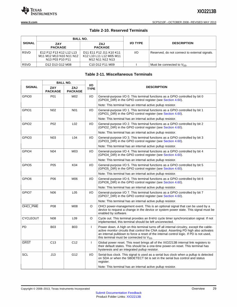
XIO2213B
www.ti.com SCPS210F –OCTOBER 2008–REVISED MAY 2013
Table 2-10. Reserved Terminals
BALL NO.SIGNAL I/O TYPE DESCRIPTIONZAY ZAJ
PACKAGE PACKAGE
RSVD E12 F12 F13 K12 L12 L13 D11 E11 F12 J11 K10 K11 I/O Reserved, do not connect to external signals.M11 M12 M13 N10 N11 N12 K12 L10 L11 L12 M05 M11
N13 P03 P10 P11 M12 N11 N12 N13
RSVD D12 D13 G12 M08 C10 D12 F11 M09 I Must be connected to VSS.
Table 2-11. Miscellaneous Terminals
BALL NO.I/OSIGNAL DESCRIPTIONZAY ZAJ TYPE
PACKAGE PACKAGE
GPIO0 P01 M02 I/O General-purpose I/O 0. This terminal functions as a GPIO controlled by bit 0(GPIO0_DIR) in the GPIO control register (see Section 4.60).
Note: This terminal has an internal active pullup resistor.
GPIO1 N02 N01 I/O General-purpose I/O 1. This terminal functions as a GPIO controlled by bit 1(GPIO1_DIR) in the GPIO control register (see Section 4.60).
Note: This terminal has an internal active pullup resistor.
GPIO2 P02 L02 I/O General-purpose I/O 2. This terminal functions as a GPIO controlled by bit 2(GPIO2_DIR) in the GPIO control register (see Section 4.60).
Note: This terminal has an internal active pullup resistor.
GPIO3 N03 L04 I/O General-purpose I/O 3. This terminal functions as a GPIO controlled by bit 3(GPIO3_DIR) in the GPIO control register (see Section 4.60).
Note: This terminal has an internal active pullup resistor.
GPIO4 N04 M03 I/O General-purpose I/O 4. This terminal functions as a GPIO controlled by bit 4(GPIO4_DIR) in the GPIO control register (see Section 4.60).
Note: This terminal has an internal active pullup resistor.
GPIO5 P05 K04 I/O General-purpose I/O 5. This terminal functions as a GPIO controlled by bit 5(GPIO5_DIR) in the GPIO control register (see Section 4.60).
Note: This terminal has an internal active pullup resistor.
GPIO6 P06 M06 I/O General-purpose I/O 6. This terminal functions as a GPIO controlled by bit 6(GPIO6_DIR) in the GPIO control register (see Section 4.60).
Note: This terminal has an internal active pullup resistor.
GPIO7 N06 L05 I/O General-purpose I/O 7. This terminal functions as a GPIO controlled by bit 7(GPIO7_DIR) in the GPIO control register (see Section 4.60).
Note: This terminal has an internal active pullup resistor.
OHCI_PME P08 M08 O OHCI power-management event. This is an optional signal that can be used by adevice to request a change in the device or system power state. This signal must beenabled by software.
CYCLEOUT N08 L09 O Cycle out. This terminal provides an 8-kHz cycle timer synchronization signal. If notimplemented, this terminal should be left unconnected.
PD B03 B03 I Power down. A high on this terminal turns off all internal circuitry, except the cable-active monitor circuits that control the CNA output. Asserting PD high also activatesan internal pulldown to force a reset of the internal control logic. If PD is not used,this terminal must be connected to VSS.
GRST C13 C12 I Global power reset. This reset brings all of the XIO2213B internal link registers totheir default states. This should be a one-time power-on reset. This terminal hashysteresis and an integrated pullup resistor.
SCL J13 G12 I/O Serial-bus clock. This signal is used as a serial bus clock when a pullup is detectedon SDA or when the SBDETECT bit is set in the serial bus control and statusregister.
Note: This terminal has an internal active pullup resistor.
Copyright © 2008–2013, Texas Instruments Incorporated Overview 29Submit Documentation FeedbackProduct Folder Links: XIO2213B
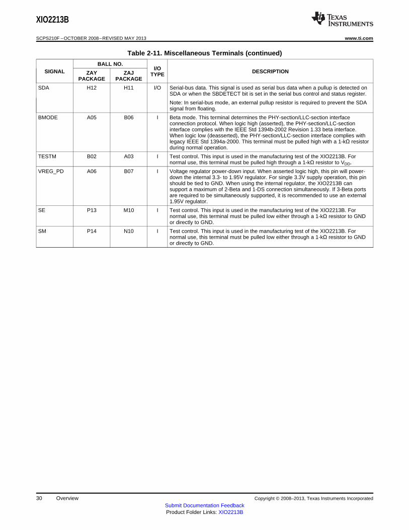
XIO2213B
SCPS210F –OCTOBER 2008–REVISED MAY 2013 www.ti.com
Table 2-11. Miscellaneous Terminals (continued)
BALL NO.I/OSIGNAL DESCRIPTIONZAY ZAJ TYPE
PACKAGE PACKAGE
SDA H12 H11 I/O Serial-bus data. This signal is used as serial bus data when a pullup is detected onSDA or when the SBDETECT bit is set in the serial bus control and status register.
Note: In serial-bus mode, an external pullup resistor is required to prevent the SDAsignal from floating.
BMODE A05 B06 I Beta mode. This terminal determines the PHY-section/LLC-section interfaceconnection protocol. When logic high (asserted), the PHY-section/LLC-sectioninterface complies with the IEEE Std 1394b-2002 Revision 1.33 beta interface.When logic low (deasserted), the PHY-section/LLC-section interface complies withlegacy IEEE Std 1394a-2000. This terminal must be pulled high with a 1-kΩ resistorduring normal operation.
TESTM B02 A03 I Test control. This input is used in the manufacturing test of the XIO2213B. Fornormal use, this terminal must be pulled high through a 1-kΩ resistor to VDD.
VREG_PD A06 B07 I Voltage regulator power-down input. When asserted logic high, this pin will power-down the internal 3.3- to 1.95V regulator. For single 3.3V supply operation, this pinshould be tied to GND. When using the internal regulator, the XIO2213B cansupport a maximum of 2-Beta and 1-DS connection simultaneously. If 3-Beta portsare required to be simultaneously supported, it is recommended to use an external1.95V regulator.
SE P13 M10 I Test control. This input is used in the manufacturing test of the XIO2213B. Fornormal use, this terminal must be pulled low either through a 1-kΩ resistor to GNDor directly to GND.
SM P14 N10 I Test control. This input is used in the manufacturing test of the XIO2213B. Fornormal use, this terminal must be pulled low either through a 1-kΩ resistor to GNDor directly to GND.
30 Overview Copyright © 2008–2013, Texas Instruments Incorporated
Submit Documentation FeedbackProduct Folder Links: XIO2213B
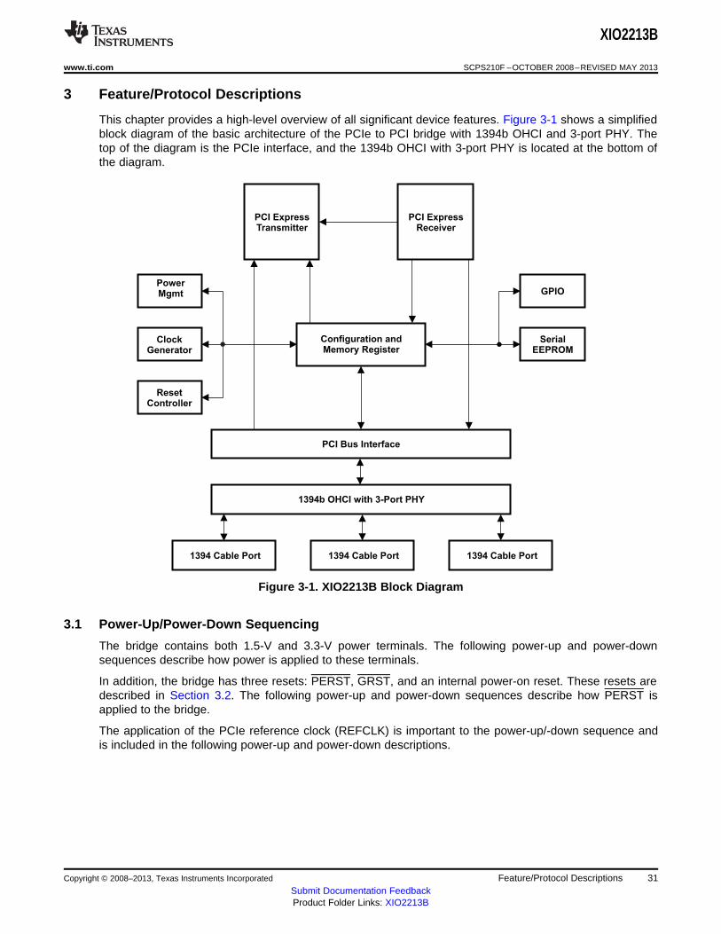
PCI ExpressTransmitter
PCI ExpressReceiver
PCI Bus Interface
Configuration andMemory Register
GPIO
SerialEEPROM
ResetController
ClockGenerator
PowerMgmt
1394b OHCI with 3-Port PHY
1394 Cable Port 1394 Cable Port 1394 Cable Port
XIO2213B
www.ti.com SCPS210F –OCTOBER 2008–REVISED MAY 2013
3 Feature/Protocol Descriptions
This chapter provides a high-level overview of all significant device features. Figure 3-1 shows a simplifiedblock diagram of the basic architecture of the PCIe to PCI bridge with 1394b OHCI and 3-port PHY. Thetop of the diagram is the PCIe interface, and the 1394b OHCI with 3-port PHY is located at the bottom ofthe diagram.
Figure 3-1. XIO2213B Block Diagram
3.1 Power-Up/Power-Down Sequencing
The bridge contains both 1.5-V and 3.3-V power terminals. The following power-up and power-downsequences describe how power is applied to these terminals.
In addition, the bridge has three resets: PERST, GRST, and an internal power-on reset. These resets aredescribed in Section 3.2. The following power-up and power-down sequences describe how PERST isapplied to the bridge.
The application of the PCIe reference clock (REFCLK) is important to the power-up/-down sequence andis included in the following power-up and power-down descriptions.
Copyright © 2008–2013, Texas Instruments Incorporated Feature/Protocol Descriptions 31Submit Documentation FeedbackProduct Folder Links: XIO2213B
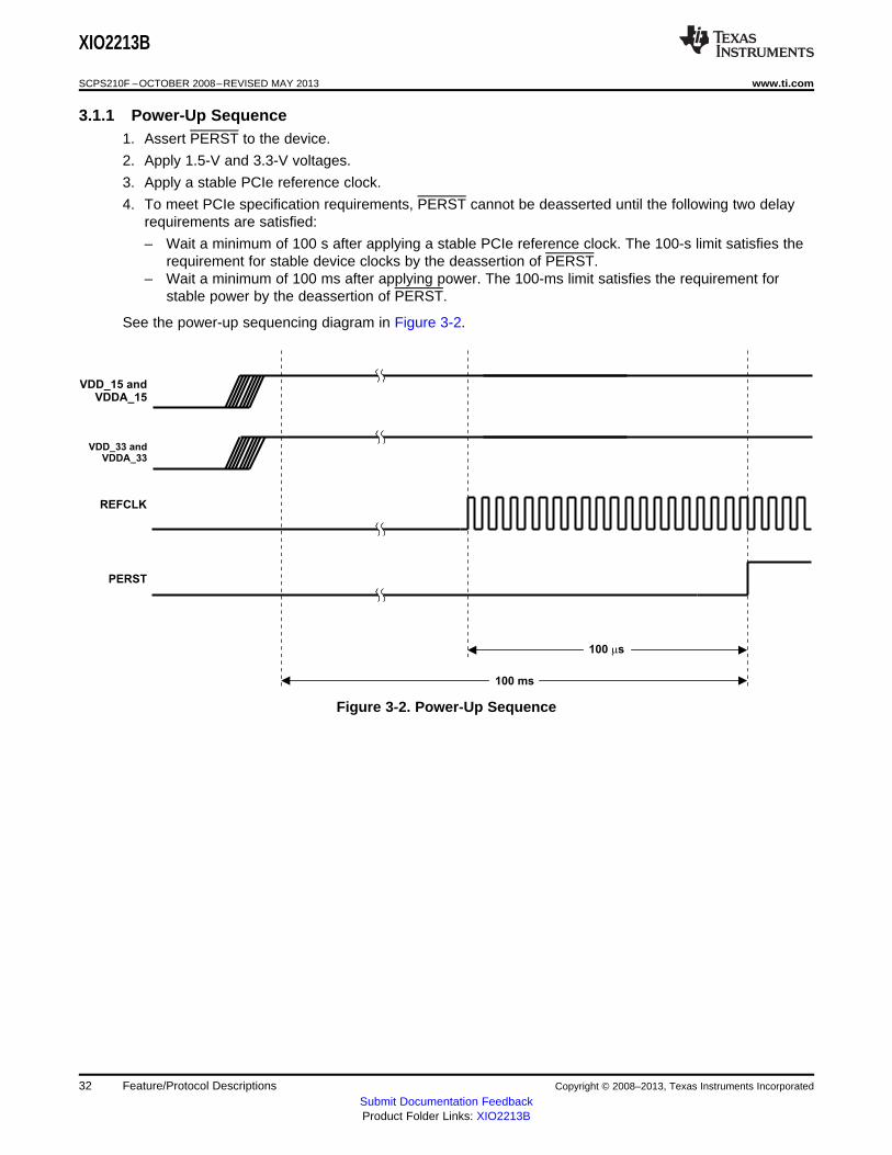
VDD_15 andVDDA_15
VDD_33 andVDDA_33
REFCLK
PERST
100 ms
100 ms
XIO2213B
SCPS210F –OCTOBER 2008–REVISED MAY 2013 www.ti.com
3.1.1 Power-Up Sequence1. Assert PERST to the device.
2. Apply 1.5-V and 3.3-V voltages.
3. Apply a stable PCIe reference clock.
4. To meet PCIe specification requirements, PERST cannot be deasserted until the following two delayrequirements are satisfied:
– Wait a minimum of 100 s after applying a stable PCIe reference clock. The 100-s limit satisfies therequirement for stable device clocks by the deassertion of PERST.
– Wait a minimum of 100 ms after applying power. The 100-ms limit satisfies the requirement forstable power by the deassertion of PERST.
See the power-up sequencing diagram in Figure 3-2.
Figure 3-2. Power-Up Sequence
32 Feature/Protocol Descriptions Copyright © 2008–2013, Texas Instruments Incorporated
Submit Documentation FeedbackProduct Folder Links: XIO2213B
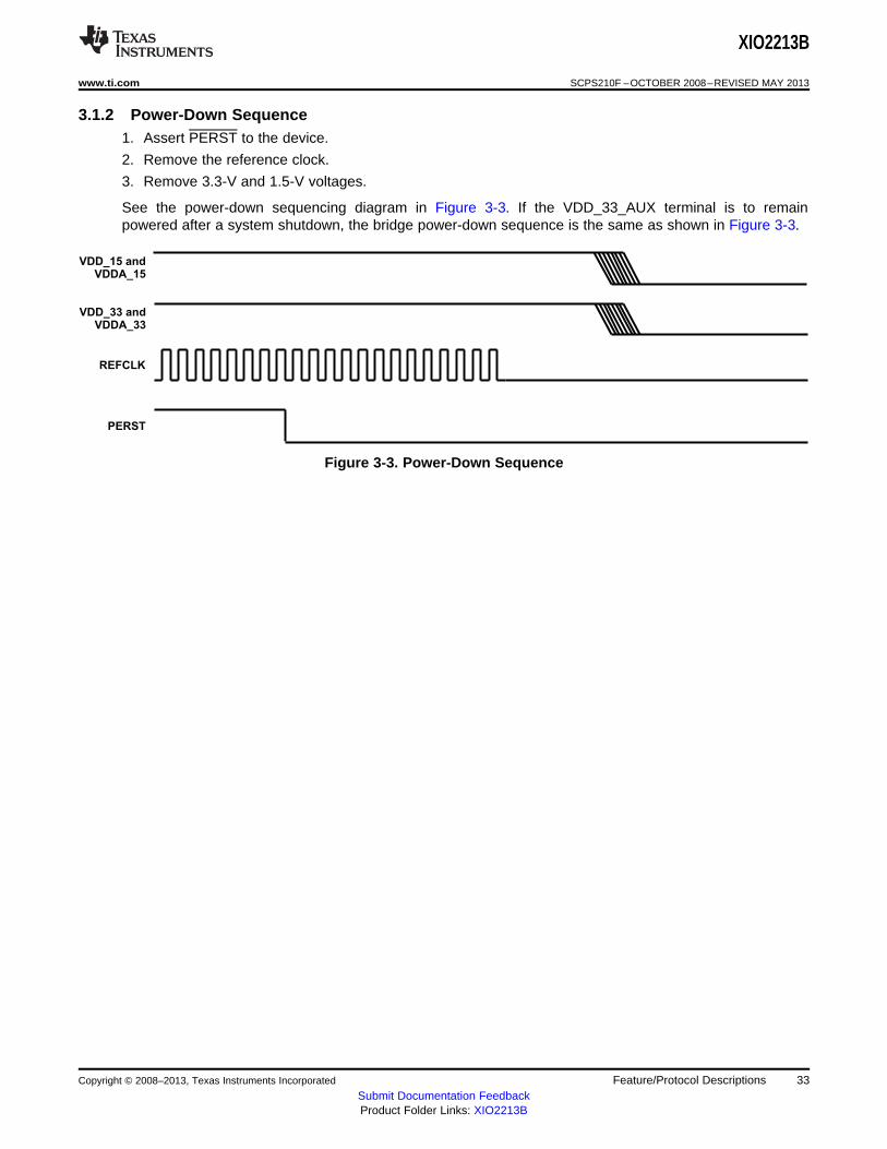
VDD_15 andVDDA_15
VDD_33 andVDDA_33
REFCLK
PERST
XIO2213B
www.ti.com SCPS210F –OCTOBER 2008–REVISED MAY 2013
3.1.2 Power-Down Sequence1. Assert PERST to the device.
2. Remove the reference clock.
3. Remove 3.3-V and 1.5-V voltages.
See the power-down sequencing diagram in Figure 3-3. If the VDD_33_AUX terminal is to remainpowered after a system shutdown, the bridge power-down sequence is the same as shown in Figure 3-3.
Figure 3-3. Power-Down Sequence
Copyright © 2008–2013, Texas Instruments Incorporated Feature/Protocol Descriptions 33Submit Documentation FeedbackProduct Folder Links: XIO2213B
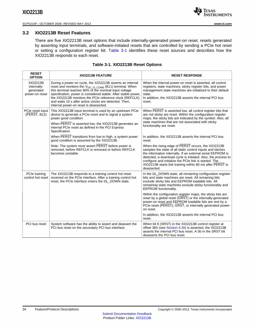
XIO2213B
SCPS210F –OCTOBER 2008–REVISED MAY 2013 www.ti.com
3.2 XIO2213B Reset Features
There are five XIO2213B reset options that include internally-generated power-on reset, resets generatedby asserting input terminals, and software-initiated resets that are controlled by sending a PCIe hot resetor setting a configuration register bit. Table 3-1 identifies these reset sources and describes how theXIO2213B responds to each reset.
Table 3-1. XIO2213B Reset Options
RESET XIO2213B FEATURE RESET RESPONSEOPTION
XIO2213B During a power-on cycle, the XIO2213B asserts an internal When the internal power-on reset is asserted, all controlinternally- reset and monitors the VDD_15_COMB (B11) terminal. When registers, state machines, sticky register bits, and powergenerated this terminal reaches 90% of the nominal input voltage management state machines are initialized to their default
power-on reset specification, power is considered stable. After stable power, state.the XIO2213B monitors the PCIe reference clock (REFCLK) In addition, the XIO2213B asserts the internal PCI busand waits 10 s after active clocks are detected. Then, reset.internal power-on reset is deasserted.
PCIe reset input This XIO2213B input terminal is used by an upstream PCIe When PERST is asserted low, all control register bits that(PERST, B12) device to generate a PCIe reset and to signal a system are not sticky are reset. Within the configuration register
power good condition. maps, the sticky bits are indicated by the symbol. Also, allstate machines that are not associated with stickyWhen PERST is asserted low, the XIO2213B generates anfunctionality are reset.internal PCIe reset as defined in the PCI Express
Specification.
When PERST transitions from low to high, a system power In addition, the XIO2213B asserts the internal PCI busgood condition is assumed by the XIO2213B. reset.
Note: The system must assert PERST before power is When the rising edge of PERST occurs, the XIO2213Bremoved, before REFCLK is removed or before REFCLK samples the state of all static control inputs and latchesbecomes unstable. the information internally. If an external serial EEPROM is
detected, a download cycle is initiated. Also, the process toconfigure and initialize the PCIe link is started. TheXIO2213B starts link training within 80 ms after PERST isdeasserted.
PCIe training The XIO2213B responds to a training control hot reset In the DL_DOWN state, all remaining configuration registercontrol hot reset received on the PCIe interface. After a training control hot bits and state machines are reset. All remaining bits
reset, the PCIe interface enters the DL_DOWN state. exclude sticky bits and EEPROM loadable bits. Allremaining state machines exclude sticky functionality andEEPROM functionality.
Within the configuration register maps, the sticky bits arereset by a global reset (GRST) or the internally-generatedpower-on reset and EEPROM loadable bits are rest by aPCIe reset (PERST), GRST, or internally generated power-on reset.
In addition, the XIO2213B asserts the internal PCI busreset.
PCI bus reset System software has the ability to assert and deassert the When bit 6 (SRST) in the XIO2213B control register atPCI bus reset on the secondary PCI bus interface. offset 3Eh (see Section 4.30) is asserted, the XIO2213B
asserts the internal PCI bus reset. A 0b in the SRST bitdeasserts the PCI bus reset.
34 Feature/Protocol Descriptions Copyright © 2008–2013, Texas Instruments Incorporated
Submit Documentation FeedbackProduct Folder Links: XIO2213B
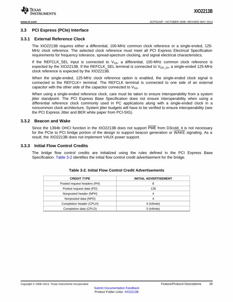
XIO2213B
www.ti.com SCPS210F –OCTOBER 2008–REVISED MAY 2013
3.3 PCI Express (PCIe) Interface
3.3.1 External Reference Clock
The XIO2213B requires either a differential, 100-MHz common clock reference or a single-ended, 125-MHz clock reference. The selected clock reference must meet all PCI Express Electrical Specificationrequirements for frequency tolerance, spread-spectrum clocking, and signal electrical characteristics.
If the REFCLK_SEL input is connected to VSS, a differential, 100-MHz common clock reference isexpected by the XIO2213B. If the REFCLK_SEL terminal is connected to VDD_33, a single-ended 125-MHzclock reference is expected by the XIO2213B.
When the single-ended, 125-MHz clock reference option is enabled, the single-ended clock signal isconnected to the REFCLK+ terminal. The REFCLK terminal is connected to one side of an externalcapacitor with the other side of the capacitor connected to VSS.
When using a single-ended reference clock, care must be taken to ensure interoperability from a systemjitter standpoint. The PCI Express Base Specification does not ensure interoperability when using adifferential reference clock commonly used in PC applications along with a single-ended clock in anoncommon clock architecture. System jitter budgets will have to be verified to ensure interoperability (seethe PCI Express Jitter and BER white paper from PCI-SIG).
3.3.2 Beacon and Wake
Since the 1394b OHCI function in the XIO2213B does not support PME from D3cold, it is not necessaryfor the PCIe to PCI bridge portion of the design to support beacon generation or WAKE signaling. As aresult, the XIO2213B does not implement VAUX power support.
3.3.3 Initial Flow Control Credits
The bridge flow control credits are initialized using the rules defined in the PCI Express BaseSpecification. Table 3-2 identifies the initial flow control credit advertisement for the bridge.
Table 3-2. Initial Flow Control Credit Advertisements
CREDIT TYPE INITIAL ADVERTISEMENT
Posted request headers (PH) 8
Posted request data (PD) 128
Nonposted header (NPH) 4
Nonposted data (NPD) 4
Completion header (CPLH) 0 (infinite)
Completion data (CPLD) 0 (infinite)
Copyright © 2008–2013, Texas Instruments Incorporated Feature/Protocol Descriptions 35Submit Documentation FeedbackProduct Folder Links: XIO2213B
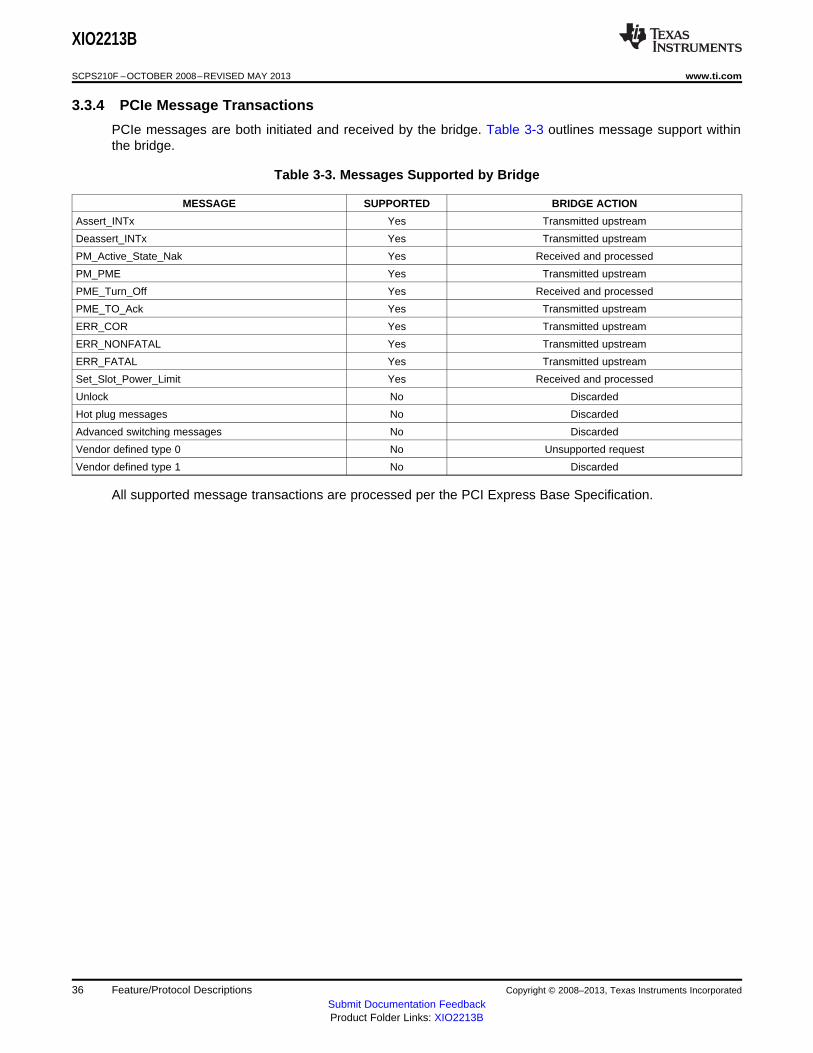
XIO2213B
SCPS210F –OCTOBER 2008–REVISED MAY 2013 www.ti.com
3.3.4 PCIe Message Transactions
PCIe messages are both initiated and received by the bridge. Table 3-3 outlines message support withinthe bridge.
Table 3-3. Messages Supported by Bridge
MESSAGE SUPPORTED BRIDGE ACTION
Assert_INTx Yes Transmitted upstream
Deassert_INTx Yes Transmitted upstream
PM_Active_State_Nak Yes Received and processed
PM_PME Yes Transmitted upstream
PME_Turn_Off Yes Received and processed
PME_TO_Ack Yes Transmitted upstream
ERR_COR Yes Transmitted upstream
ERR_NONFATAL Yes Transmitted upstream
ERR_FATAL Yes Transmitted upstream
Set_Slot_Power_Limit Yes Received and processed
Unlock No Discarded
Hot plug messages No Discarded
Advanced switching messages No Discarded
Vendor defined type 0 No Unsupported request
Vendor defined type 1 No Discarded
All supported message transactions are processed per the PCI Express Base Specification.
36 Feature/Protocol Descriptions Copyright © 2008–2013, Texas Instruments Incorporated
Submit Documentation FeedbackProduct Folder Links: XIO2213B
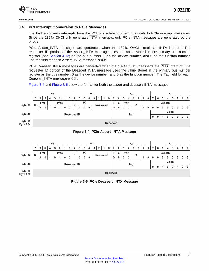
R
+0 +1 +2 +3
01234567012345677 6 5 4 3 2 1 07 6 5 4 3 2 1 0
TypeFmt
0 1 1 0 1 0 0R
TCReserved
Reserved ID
0 0 0
Reserved
Tag
RLength
Code
Attr
0000000000
00100100
ET
PD 00Byte 0>
Byte 4>
Byte 8>Byte 12>
R
+0 +1 +2 +3
01234567012345677 6 5 4 3 2 1 07 6 5 4 3 2 1 0
TypeFmt
0 1 1 0 1 0 0R
TCReserved
Reserved ID
0 0 0
Reserved
Tag
RLength
Code
Attr
0000000000
00000100
ET
PD 00Byte 0>
Byte 4>
Byte 8>Byte 12>
XIO2213B
www.ti.com SCPS210F –OCTOBER 2008–REVISED MAY 2013
3.4 PCI Interrupt Conversion to PCIe Messages
The bridge converts interrupts from the PCI bus sideband interrupt signals to PCIe interrupt messages.Since the 1394a OHCI only generates INTA interrupts, only PCIe INTA messages are generated by thebridge.
PCIe Assert_INTA messages are generated when the 1394a OHCI signals an INTA interrupt. Therequester ID portion of the Assert_INTA message uses the value stored in the primary bus numberregister (see Section 4.12) as the bus number, 0 as the device number, and 0 as the function number.The tag field for each Assert_INTA message is 00h.
PCIe Deassert_INTA messages are generated when the 1394a OHCI deasserts the INTA interrupt. Therequester ID portion of the Deassert_INTA message uses the value stored in the primary bus numberregister as the bus number, 0 as the device number, and 0 as the function number. The Tag field for eachDeassert_INTA message is 00h.
Figure 3-4 and Figure 3-5 show the format for both the assert and deassert INTA messages.
Figure 3-4. PCIe Assert_INTA Message
Figure 3-5. PCIe Deassert_INTX Message
Copyright © 2008–2013, Texas Instruments Incorporated Feature/Protocol Descriptions 37Submit Documentation FeedbackProduct Folder Links: XIO2213B
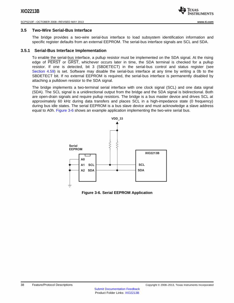
SCL
SDA
VDD_33
A0
A1
A2
SCL
SDA
XIO2213B
SerialEEPROM
XIO2213B
SCPS210F –OCTOBER 2008–REVISED MAY 2013 www.ti.com
3.5 Two-Wire Serial-Bus Interface
The bridge provides a two-wire serial-bus interface to load subsystem identification information andspecific register defaults from an external EEPROM. The serial-bus interface signals are SCL and SDA.
3.5.1 Serial-Bus Interface Implementation
To enable the serial-bus interface, a pullup resistor must be implemented on the SDA signal. At the risingedge of PERST or GRST, whichever occurs later in time, the SDA terminal is checked for a pullupresistor. If one is detected, bit 3 (SBDETECT) in the serial-bus control and status register (seeSection 4.59) is set. Software may disable the serial-bus interface at any time by writing a 0b to theSBDETECT bit. If no external EEPROM is required, the serial-bus interface is permanently disabled byattaching a pulldown resistor to the SDA signal.
The bridge implements a two-terminal serial interface with one clock signal (SCL) and one data signal(SDA). The SCL signal is a unidirectional output from the bridge and the SDA signal is bidirectional. Bothare open-drain signals and require pullup resistors. The bridge is a bus master device and drives SCL atapproximately 60 kHz during data transfers and places SCL in a high-impedance state (0 frequency)during bus idle states. The serial EEPROM is a bus slave device and must acknowledge a slave addressequal to A0h. Figure 3-6 shows an example application implementing the two-wire serial bus.
Figure 3-6. Serial EEPROM Application
38 Feature/Protocol Descriptions Copyright © 2008–2013, Texas Instruments Incorporated
Submit Documentation FeedbackProduct Folder Links: XIO2213B
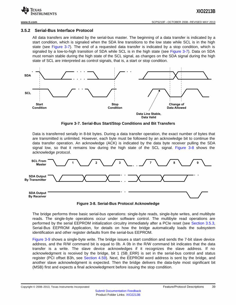
SCL FromMaster
1 2 3 7 8 9
SDA OutputBy Transmitter
SDA OutputBy Receiver
SDA
SCL
StartCondition
StopCondition
Change ofData Allowed
Data Line Stable,Data Valid
XIO2213B
www.ti.com SCPS210F –OCTOBER 2008–REVISED MAY 2013
3.5.2 Serial-Bus Interface Protocol
All data transfers are initiated by the serial-bus master. The beginning of a data transfer is indicated by astart condition, which is signaled when the SDA line transitions to the low state while SCL is in the highstate (see Figure 3-7). The end of a requested data transfer is indicated by a stop condition, which issignaled by a low-to-high transition of SDA while SCL is in the high state (see Figure 3-7). Data on SDAmust remain stable during the high state of the SCL signal, as changes on the SDA signal during the highstate of SCL are interpreted as control signals, that is, a start or stop condition.
Figure 3-7. Serial-Bus Start/Stop Conditions and Bit Transfers
Data is transferred serially in 8-bit bytes. During a data transfer operation, the exact number of bytes thatare transmitted is unlimited. However, each byte must be followed by an acknowledge bit to continue thedata transfer operation. An acknowledge (ACK) is indicated by the data byte receiver pulling the SDAsignal low, so that it remains low during the high state of the SCL signal. Figure 3-8 shows theacknowledge protocol.
Figure 3-8. Serial-Bus Protocol Acknowledge
The bridge performs three basic serial-bus operations: single-byte reads, single-byte writes, and multibytereads. The single-byte operations occur under software control. The multibyte read operations areperformed by the serial EEPROM initialization circuitry immediately after a PCIe reset (see Section 3.5.3,Serial-Bus EEPROM Application, for details on how the bridge automatically loads the subsystemidentification and other register defaults from the serial-bus EEPROM.
Figure 3-9 shows a single-byte write. The bridge issues a start condition and sends the 7-bit slave deviceaddress, and the R/W command bit is equal to 0b. A 0b in the R/W command bit indicates that the datatransfer is a write. The slave device acknowledges if it recognizes the slave address. If noacknowledgment is received by the bridge, bit 1 (SB_ERR) is set in the serial-bus control and statusregister (PCI offset B3h, see Section 4.59). Next, the EEPROM word address is sent by the bridge, andanother slave acknowledgment is expected. Then the bridge delivers the data-byte most significant bit(MSB) first and expects a final acknowledgment before issuing the stop condition.
Copyright © 2008–2013, Texas Instruments Incorporated Feature/Protocol Descriptions 39Submit Documentation FeedbackProduct Folder Links: XIO2213B
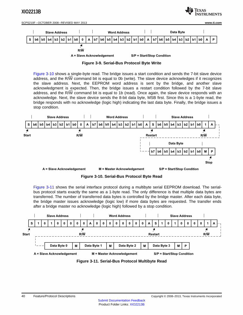
S 1 10 0 0 0 0 0 0 0 0 0 0 0 0 0A A
Slave Address Word Address
R/W
Data Byte 1 Data Byte 2 Data Byte 3 M PMM
M = Master Acknowledgement S/P = Start/Stop ConditionA = Slave Acknowledgement
Data Byte 0 M
S 1 10 0 0 0 0 1 A
Restart R/W
Slave Address
Start
S b6 b4b5 b3 b2 b1 b0 0 b7 b6 b5 b4 b3 b2 b1 b0A A
Slave Address Word Address
R/W
S b6 b4b5 b3 b2 b1 b0 1 A
Slave Address
S/P = Start/Stop ConditionM = Master Acknowledgement
b7 b6 b4b5 b3 b2 b1 b0 M P
Data Byte
Start Restart R/W
A = Slave Acknowledgement
Stop
S b6 b4b5 b3 b2 b1 b0 0 b7 b6 b5 b4 b3 b2 b1 b0A A
Slave Address Word Address
R/W
S/P = Start/Stop ConditionA = Slave Acknowledgement
b7 b6 b4b5 b3 b2 b1 b0 A P
Data Byte
XIO2213B
SCPS210F –OCTOBER 2008–REVISED MAY 2013 www.ti.com
Figure 3-9. Serial-Bus Protocol Byte Write
Figure 3-10 shows a single-byte read. The bridge issues a start condition and sends the 7-bit slave deviceaddress, and the R/W command bit is equal to 0b (write). The slave device acknowledges if it recognizesthe slave address. Next, the EEPROM word address is sent by the bridge, and another slaveacknowledgment is expected. Then, the bridge issues a restart condition followed by the 7-bit slaveaddress, and the R/W command bit is equal to 1b (read). Once again, the slave device responds with anacknowledge. Next, the slave device sends the 8-bit data byte, MSB first. Since this is a 1-byte read, thebridge responds with no acknowledge (logic high) indicating the last data byte. Finally, the bridge issues astop condition.
Figure 3-10. Serial-Bus Protocol Byte Read
Figure 3-11 shows the serial interface protocol during a multibyte serial EEPROM download. The serial-bus protocol starts exactly the same as a 1-byte read. The only difference is that multiple data bytes aretransferred. The number of transferred data bytes is controlled by the bridge master. After each data byte,the bridge master issues acknowledge (logic low) if more data bytes are requested. The transfer endsafter a bridge master no acknowledge (logic high) followed by a stop condition.
Figure 3-11. Serial-Bus Protocol Multibyte Read
40 Feature/Protocol Descriptions Copyright © 2008–2013, Texas Instruments Incorporated
Submit Documentation FeedbackProduct Folder Links: XIO2213B
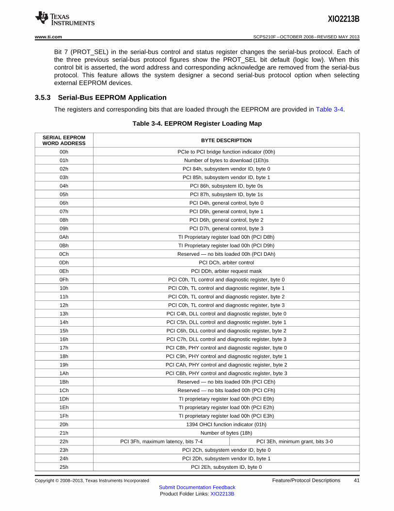
XIO2213B
www.ti.com SCPS210F –OCTOBER 2008–REVISED MAY 2013
Bit 7 (PROT_SEL) in the serial-bus control and status register changes the serial-bus protocol. Each ofthe three previous serial-bus protocol figures show the PROT_SEL bit default (logic low). When thiscontrol bit is asserted, the word address and corresponding acknowledge are removed from the serial-busprotocol. This feature allows the system designer a second serial-bus protocol option when selectingexternal EEPROM devices.
3.5.3 Serial-Bus EEPROM Application
The registers and corresponding bits that are loaded through the EEPROM are provided in Table 3-4.
Table 3-4. EEPROM Register Loading Map
SERIAL EEPROM BYTE DESCRIPTIONWORD ADDRESS
00h PCIe to PCI bridge function indicator (00h)
01h Number of bytes to download (1Eh)s
02h PCI 84h, subsystem vendor ID, byte 0
03h PCI 85h, subsystem vendor ID, byte 1
04h PCI 86h, subsystem ID, byte 0s
05h PCI 87h, subsystem ID, byte 1s
06h PCI D4h, general control, byte 0
07h PCI D5h, general control, byte 1
08h PCI D6h, general control, byte 2
09h PCI D7h, general control, byte 3
0Ah TI Proprietary register load 00h (PCI D8h)
0Bh TI Proprietary register load 00h (PCI D9h)
0Ch Reserved — no bits loaded 00h (PCI DAh)
0Dh PCI DCh, arbiter control
0Eh PCI DDh, arbiter request mask
0Fh PCI C0h, TL control and diagnostic register, byte 0
10h PCI C0h, TL control and diagnostic register, byte 1
11h PCI C0h, TL control and diagnostic register, byte 2
12h PCI C0h, TL control and diagnostic register, byte 3
13h PCI C4h, DLL control and diagnostic register, byte 0
14h PCI C5h, DLL control and diagnostic register, byte 1
15h PCI C6h, DLL control and diagnostic register, byte 2
16h PCI C7h, DLL control and diagnostic register, byte 3
17h PCI C8h, PHY control and diagnostic register, byte 0
18h PCI C9h, PHY control and diagnostic register, byte 1
19h PCI CAh, PHY control and diagnostic register, byte 2
1Ah PCI CBh, PHY control and diagnostic register, byte 3
1Bh Reserved — no bits loaded 00h (PCI CEh)
1Ch Reserved — no bits loaded 00h (PCI CFh)
1Dh TI proprietary register load 00h (PCI E0h)
1Eh TI proprietary register load 00h (PCI E2h)
1Fh TI proprietary register load 00h (PCI E3h)
20h 1394 OHCI function indicator (01h)
21h Number of bytes (18h)
22h PCI 3Fh, maximum latency, bits 7-4 PCI 3Eh, minimum grant, bits 3-0
23h PCI 2Ch, subsystem vendor ID, byte 0
24h PCI 2Dh, subsystem vendor ID, byte 1
25h PCI 2Eh, subsystem ID, byte 0
Copyright © 2008–2013, Texas Instruments Incorporated Feature/Protocol Descriptions 41Submit Documentation FeedbackProduct Folder Links: XIO2213B
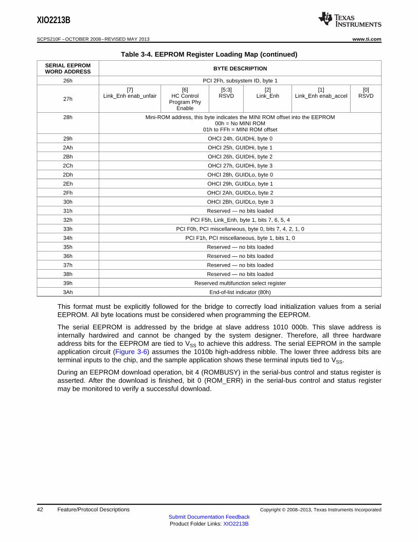
XIO2213B
SCPS210F –OCTOBER 2008–REVISED MAY 2013 www.ti.com
Table 3-4. EEPROM Register Loading Map (continued)
SERIAL EEPROM BYTE DESCRIPTIONWORD ADDRESS
26h PCI 2Fh, subsystem ID, byte 1
[7] [6] [5:3] [2] [1] [0]Link_Enh enab_unfair HC Control RSVD Link_Enh Link_Enh enab_accel RSVD27h Program Phy
Enable
28h Mini-ROM address, this byte indicates the MINI ROM offset into the EEPROM00h = No MINI ROM
01h to FFh = MINI ROM offset
29h OHCI 24h, GUIDHi, byte 0
2Ah OHCI 25h, GUIDHi, byte 1
2Bh OHCI 26h, GUIDHi, byte 2
2Ch OHCI 27h, GUIDHi, byte 3
2Dh OHCI 28h, GUIDLo, byte 0
2Eh OHCI 29h, GUIDLo, byte 1
2Fh OHCI 2Ah, GUIDLo, byte 2
30h OHCI 2Bh, GUIDLo, byte 3
31h Reserved — no bits loaded
32h PCI F5h, Link_Enh, byte 1, bits 7, 6, 5, 4
33h PCI F0h, PCI miscellaneous, byte 0, bits 7, 4, 2, 1, 0
34h PCI F1h, PCI miscellaneous, byte 1, bits 1, 0
35h Reserved — no bits loaded
36h Reserved — no bits loaded
37h Reserved — no bits loaded
38h Reserved — no bits loaded
39h Reserved multifunction select register
3Ah End-of-list indicator (80h)
This format must be explicitly followed for the bridge to correctly load initialization values from a serialEEPROM. All byte locations must be considered when programming the EEPROM.
The serial EEPROM is addressed by the bridge at slave address 1010 000b. This slave address isinternally hardwired and cannot be changed by the system designer. Therefore, all three hardwareaddress bits for the EEPROM are tied to VSS to achieve this address. The serial EEPROM in the sampleapplication circuit (Figure 3-6) assumes the 1010b high-address nibble. The lower three address bits areterminal inputs to the chip, and the sample application shows these terminal inputs tied to VSS.
During an EEPROM download operation, bit 4 (ROMBUSY) in the serial-bus control and status register isasserted. After the download is finished, bit 0 (ROM_ERR) in the serial-bus control and status registermay be monitored to verify a successful download.
42 Feature/Protocol Descriptions Copyright © 2008–2013, Texas Instruments Incorporated
Submit Documentation FeedbackProduct Folder Links: XIO2213B
XIO2213B
www.ti.com SCPS210F –OCTOBER 2008–REVISED MAY 2013
3.5.4 Accessing Serial-Bus Devices Through Softwaree
The bridge provides a programming mechanism to control serial-bus devices through system software.The programming is accomplished through a doubleword of PCI configuration space at offset B0h.Table 3-5 lists the registers that program a serial-bus device through software.
Table 3-5. Registers Used To Program Serial-Bus Devices
PCI OFFSET REGISTER NAME DESCRIPTION
B0h Serial-bus data Contains the data byte to send on write commands or the received data byte on read(see Section 4.56) commands.
B1h Serial-bus word address The content of this register is sent as the word address on byte writes or reads. This register is(see Section 4.57) not used in the quick command protocol. Bit 7 (PROT_SEL) in the serial-bus control and status
register (offset B3h, see Section 4.59) is set to 1b to enable the slave address to be sent.
B2h Serial-bus slave address Write transactions to this register initiate a serial-bus transaction. The slave device address and(see Section 4.58) the R/W command selector are programmed through this register.
B3h Serial-bus control and Serial interface enable, busy, and error status are communicated through this register. Instatus (see Section 4.59) addition, the protocol-select bit (PROT_SEL) and serial-bus test bit (SBTEST) are programmed
through this register.
To access the serial EEPROM through the software interface, the following steps are performed:
1. The control and status byte is read to verify the EEPROM interface is enabled (SBDETECT asserted)and not busy (REQBUSY and ROMBUSY deasserted).
2. The serial-bus word address is loaded. If the access is a write, the data byte is also loaded.
3. The serial-bus slave address and R/W command selector byte is written.
4. REQBUSY is monitored until this bit is deasserted.
5. SB_ERR is checked to verify that the serial-bus operation completed without error. If the operation is aread, the serial-bus data byte is now valid.
3.6 Advanced Error Reporting Registers
In the extended PCIe configuration space, the bridge supports the advanced error reporting capabilitiesstructure. For the PCIe interface, both correctable and uncorrectable error statuses are provided. For thePCI bus interface, secondary uncorrectable error status is provided. All uncorrectable status bits havecorresponding mask and severity control bits. For correctable status bits, only mask bits are provided.
Both the primary and secondary interfaces include first error pointer and header log registers. When thefirst error is detected, the corresponding bit position within the uncorrectable status register is loaded intothe first error pointer register. Likewise, the header information associated with the first failing transactionis loaded into the header log. To reset this first error control logic, the corresponding status bit in theuncorrectable status register is cleared by a writeback of 1b.
For systems that require high data reliability, ECRC is fully supported on the PCIe interface. The primary-side advanced error capabilities and control register has both ECRC generation and checking enablecontrol bits. When the checking bit is asserted, all received TLPs are checked for a valid ECRC field. If thegeneration bit is asserted, all transmitted TLPs contain a valid ECRC field.
3.7 Data Error Forwarding Capability
The bridge supports the transfer of data errors in both directions.
If a downstream PCIe transaction with a data payload is received that targets the internal PCI bus and theEP bit is set indicating poisoned data, the bridge must ensure that this information is transferred to the PCIbus. To do this, the bridge forces a parity error on each PCI bus data phase by inverting the parity bitcalculated for each double word of data.
If the bridge is the target of a PCI transaction that is forwarded to the PCIe interface and a data parityerror is detected, this information is passed to the PCIe interface. To do this, the bridge sets the EP bit inthe upstream PCIe header.
Copyright © 2008–2013, Texas Instruments Incorporated Feature/Protocol Descriptions 43Submit Documentation FeedbackProduct Folder Links: XIO2213B
XIO2213B
SCPS210F –OCTOBER 2008–REVISED MAY 2013 www.ti.com
3.8 General-Purpose I/O (GPIO) Interface
Up to eight GPIO terminals are provided for system customization. These GPIO terminals are 3.3-Vtolerant.
The exact number of GPIO terminals varies based on implementing the clock-run, power-override, andserial EEPROM interface features. These features share four of the eight GPIO terminals. When any ofthe three shared functions are enabled, the associated GPIO terminal is disabled.
All eight GPIO terminals are individually configurable as either inputs or outputs by writing thecorresponding bit in the GPIO control register at offset B4h. A GPIO data register at offset B6h exists toeither read the logic state of each GPIO input or to set the logic state of each GPIO output. The power-updefault state for the GPIO control register is input mode.
3.9 Set Slot Power Limit Functionality
The PCI Express Specification provides a method for devices to limit internal functionality and save powerbased on the value programmed into the captured slot power limit scale (CSPLS) and capture slot powerlimit value (CSPLV) fields of the PCIe device capabilities register at offset 94h (see Section 4.50, DeviceCapabilities Register, for details). The bridge writes these fields when a set slot power limit message isreceived on the PCIe interface.
After the deassertion of PERST, the XIO2213B compares the information within the CSPLS and CSPLVfields of the device capabilities register to the minimum power scale (MIN_POWER_SCALE) and minimumpower value (MIN_POWER_VALUE) fields in the general control register at offset D4h (see Section 4.66,General Control Register, for details). If the CSPLS and CSPLV fields are less than theMIN_POWER_SCALE and MIN_POWER_VALUE fields, respectively, the bridge takes the appropriateaction that is defined below.
The power usage action is programmable within the bridge. The general control register includes a 3-bitPOWER_OVRD field. This field is programmable to the following two options:• Ignore slot power limit fields.• Respond with unsupported request to all transactions except type 0/1 configuration transactions, and
set slot power limit messages.
3.10 PCIe and PCI Bus Power Management
The bridge supports both software-directed power management and active-state power managementthrough standard PCI configuration space. Software-directed registers are located in the powermanagement capabilities structure located at offset 50h. Active-state power management control registersare located in the PCIe capabilities structure located at offset 90h.
During software-directed power-management state changes, the bridge initiates link state transitions to L1or L2/L3 after a configuration write transaction places the device in a low-power state. The power-management state machine is also responsible for gating internal clocks based on the power state.Table 3-6 identifies the relationship between the D-states and bridge clock operation.
Table 3-6. Clocking In Low Power States
CLOCK SOURCE D0/L0 D1/L1 D2/L1 D3/L2/L3
PCIe reference clock input (REFCLK) On On On On/Off
Internal PCI bus clock to bridge function On Off Off Off
Internal PCI bus clock to 1394b OHCI function On On On On/Off
44 Feature/Protocol Descriptions Copyright © 2008–2013, Texas Instruments Incorporated
Submit Documentation FeedbackProduct Folder Links: XIO2213B
XIO2213B
www.ti.com SCPS210F –OCTOBER 2008–REVISED MAY 2013
The link power management (LPM) state machine manages active-state power by monitoring the PCIetransaction activity. If no transactions are pending and the transmitter has been idle for at least theminimum time required by the PCI Express Specification, the LPM state machine transitions the link toeither the L0s or L1 state. By reading the bridges L0s and L1 exit latency in the link capabilities register,the system software may make an informed decision relating to system performance versus powersavings. The ASLPMC field in the link control register provides an L0s-only option, L1-only option, or bothL0s and L1 options.
Finally, the bridge generates the PM_Active_State_Nak Message if a PM_Active_State_Request_L1DLLP is received on the PCIe interface and the link cannot be transitioned to L1.
Copyright © 2008–2013, Texas Instruments Incorporated Feature/Protocol Descriptions 45Submit Documentation FeedbackProduct Folder Links: XIO2213B
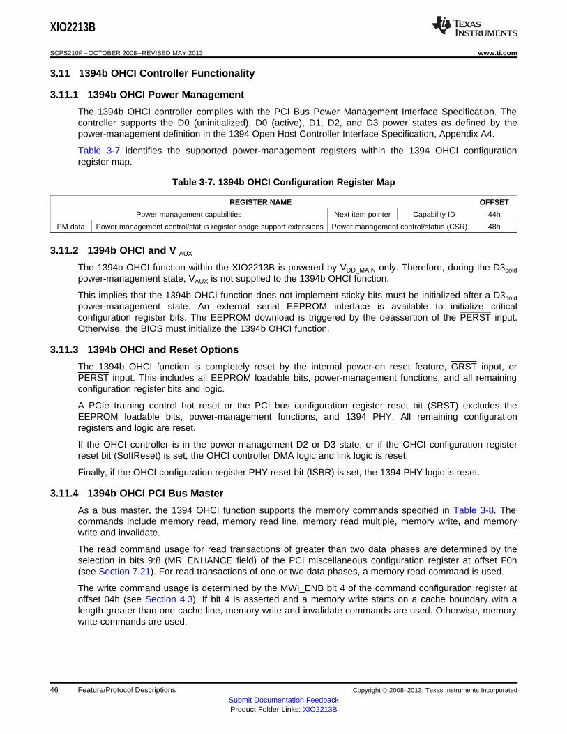
XIO2213B
SCPS210F –OCTOBER 2008–REVISED MAY 2013 www.ti.com
3.11 1394b OHCI Controller Functionality
3.11.1 1394b OHCI Power Management
The 1394b OHCI controller complies with the PCI Bus Power Management Interface Specification. Thecontroller supports the D0 (uninitialized), D0 (active), D1, D2, and D3 power states as defined by thepower-management definition in the 1394 Open Host Controller Interface Specification, Appendix A4.
Table 3-7 identifies the supported power-management registers within the 1394 OHCI configurationregister map.
Table 3-7. 1394b OHCI Configuration Register Map
REGISTER NAME OFFSET
Power management capabilities Next item pointer Capability ID 44h
PM data Power management control/status register bridge support extensions Power management control/status (CSR) 48h
3.11.2 1394b OHCI and V AUX
The 1394b OHCI function within the XIO2213B is powered by VDD_MAIN only. Therefore, during the D3coldpower-management state, VAUX is not supplied to the 1394b OHCI function.
This implies that the 1394b OHCI function does not implement sticky bits must be initialized after a D3coldpower-management state. An external serial EEPROM interface is available to initialize criticalconfiguration register bits. The EEPROM download is triggered by the deassertion of the PERST input.Otherwise, the BIOS must initialize the 1394b OHCI function.
3.11.3 1394b OHCI and Reset Options
The 1394b OHCI function is completely reset by the internal power-on reset feature, GRST input, orPERST input. This includes all EEPROM loadable bits, power-management functions, and all remainingconfiguration register bits and logic.
A PCIe training control hot reset or the PCI bus configuration register reset bit (SRST) excludes theEEPROM loadable bits, power-management functions, and 1394 PHY. All remaining configurationregisters and logic are reset.
If the OHCI controller is in the power-management D2 or D3 state, or if the OHCI configuration registerreset bit (SoftReset) is set, the OHCI controller DMA logic and link logic is reset.
Finally, if the OHCI configuration register PHY reset bit (ISBR) is set, the 1394 PHY logic is reset.
3.11.4 1394b OHCI PCI Bus Master
As a bus master, the 1394 OHCI function supports the memory commands specified in Table 3-8. Thecommands include memory read, memory read line, memory read multiple, memory write, and memorywrite and invalidate.
The read command usage for read transactions of greater than two data phases are determined by theselection in bits 9:8 (MR_ENHANCE field) of the PCI miscellaneous configuration register at offset F0h(see Section 7.21). For read transactions of one or two data phases, a memory read command is used.
The write command usage is determined by the MWI_ENB bit 4 of the command configuration register atoffset 04h (see Section 4.3). If bit 4 is asserted and a memory write starts on a cache boundary with alength greater than one cache line, memory write and invalidate commands are used. Otherwise, memorywrite commands are used.
46 Feature/Protocol Descriptions Copyright © 2008–2013, Texas Instruments Incorporated
Submit Documentation FeedbackProduct Folder Links: XIO2213B
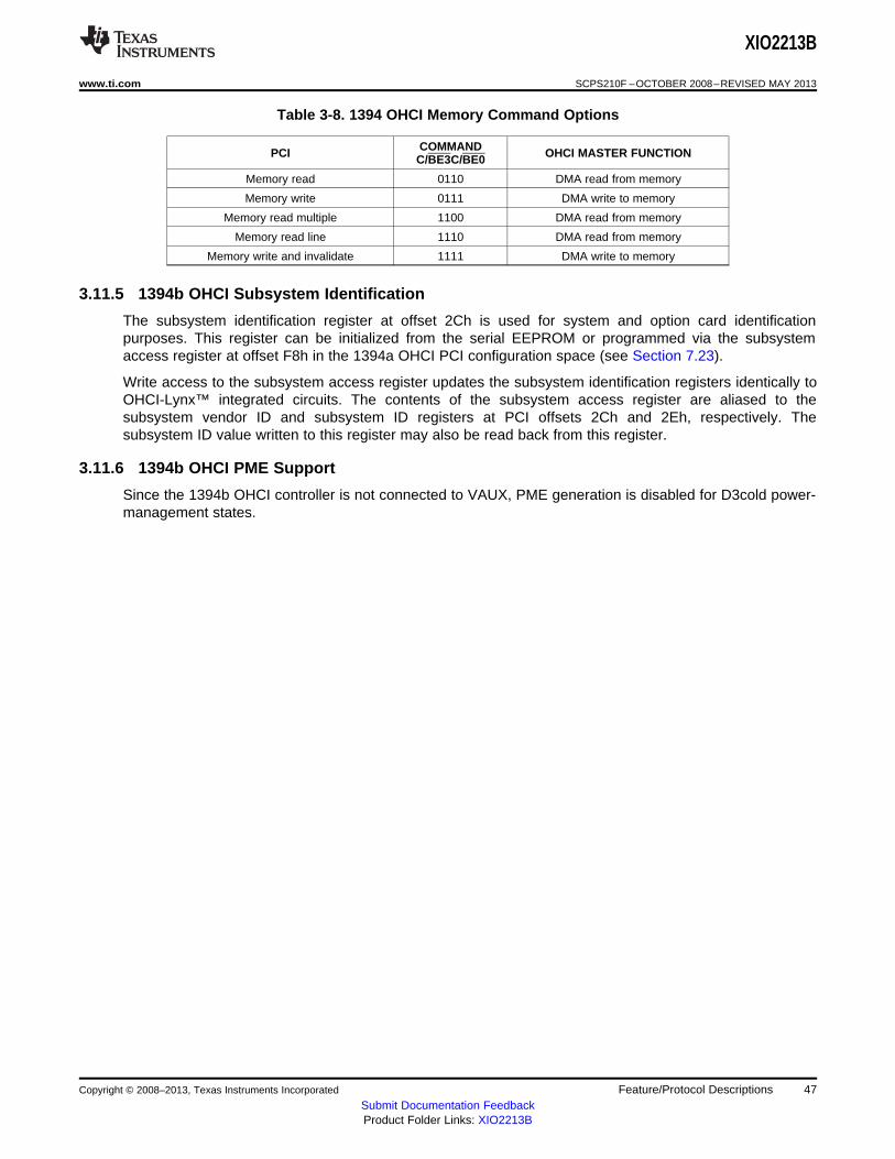
XIO2213B
www.ti.com SCPS210F –OCTOBER 2008–REVISED MAY 2013
Table 3-8. 1394 OHCI Memory Command Options
COMMANDPCI OHCI MASTER FUNCTIONC/BE3C/BE0
Memory read 0110 DMA read from memory
Memory write 0111 DMA write to memory
Memory read multiple 1100 DMA read from memory
Memory read line 1110 DMA read from memory
Memory write and invalidate 1111 DMA write to memory
3.11.5 1394b OHCI Subsystem Identification
The subsystem identification register at offset 2Ch is used for system and option card identificationpurposes. This register can be initialized from the serial EEPROM or programmed via the subsystemaccess register at offset F8h in the 1394a OHCI PCI configuration space (see Section 7.23).
Write access to the subsystem access register updates the subsystem identification registers identically toOHCI-Lynx™ integrated circuits. The contents of the subsystem access register are aliased to thesubsystem vendor ID and subsystem ID registers at PCI offsets 2Ch and 2Eh, respectively. Thesubsystem ID value written to this register may also be read back from this register.
3.11.6 1394b OHCI PME Support
Since the 1394b OHCI controller is not connected to VAUX, PME generation is disabled for D3cold power-management states.
Copyright © 2008–2013, Texas Instruments Incorporated Feature/Protocol Descriptions 47Submit Documentation FeedbackProduct Folder Links: XIO2213B
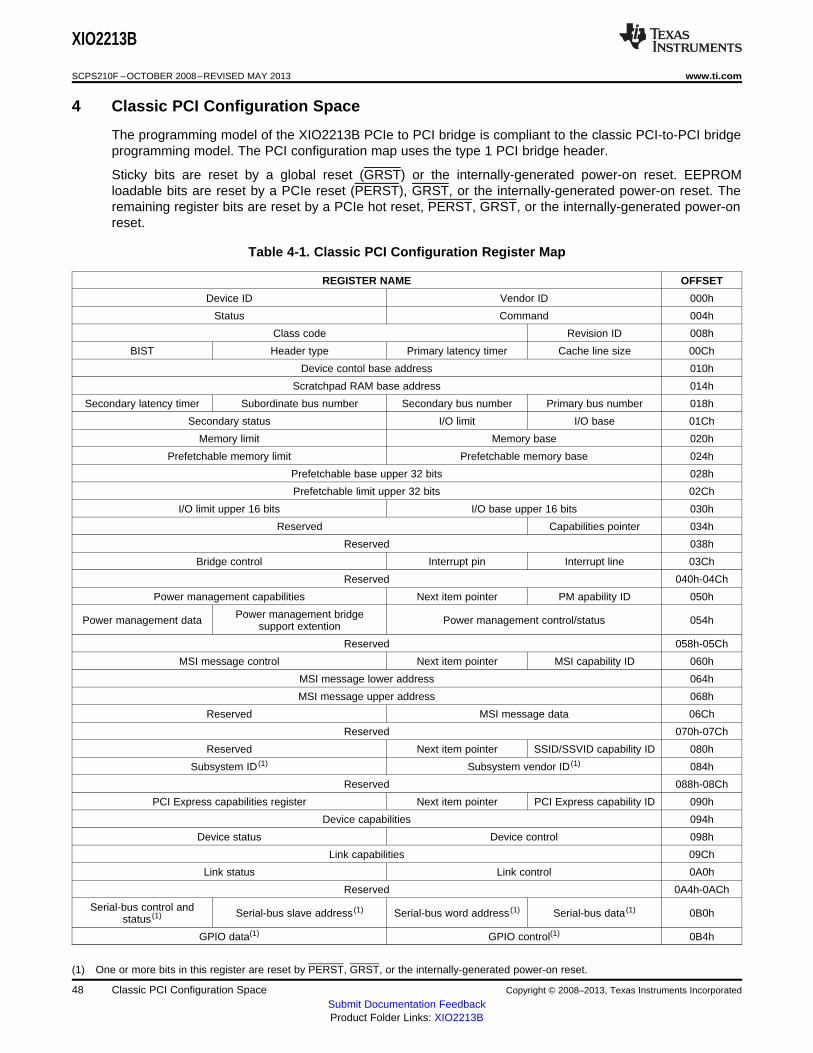
XIO2213B
SCPS210F –OCTOBER 2008–REVISED MAY 2013 www.ti.com
4 Classic PCI Configuration Space
The programming model of the XIO2213B PCIe to PCI bridge is compliant to the classic PCI-to-PCI bridgeprogramming model. The PCI configuration map uses the type 1 PCI bridge header.
Sticky bits are reset by a global reset (GRST) or the internally-generated power-on reset. EEPROMloadable bits are reset by a PCIe reset (PERST), GRST, or the internally-generated power-on reset. Theremaining register bits are reset by a PCIe hot reset, PERST, GRST, or the internally-generated power-onreset.
Table 4-1. Classic PCI Configuration Register Map
REGISTER NAME OFFSET
Device ID Vendor ID 000h
Status Command 004h
Class code Revision ID 008h
BIST Header type Primary latency timer Cache line size 00Ch
Device contol base address 010h
Scratchpad RAM base address 014h
Secondary latency timer Subordinate bus number Secondary bus number Primary bus number 018h
Secondary status I/O limit I/O base 01Ch
Memory limit Memory base 020h
Prefetchable memory limit Prefetchable memory base 024h
Prefetchable base upper 32 bits 028h
Prefetchable limit upper 32 bits 02Ch
I/O limit upper 16 bits I/O base upper 16 bits 030h
Reserved Capabilities pointer 034h
Reserved 038h
Bridge control Interrupt pin Interrupt line 03Ch
Reserved 040h-04Ch
Power management capabilities Next item pointer PM apability ID 050h
Power management bridgePower management data Power management control/status 054hsupport extention
Reserved 058h-05Ch
MSI message control Next item pointer MSI capability ID 060h
MSI message lower address 064h
MSI message upper address 068h
Reserved MSI message data 06Ch
Reserved 070h-07Ch
Reserved Next item pointer SSID/SSVID capability ID 080h
Subsystem ID (1) Subsystem vendor ID (1) 084h
Reserved 088h-08Ch
PCI Express capabilities register Next item pointer PCI Express capability ID 090h
Device capabilities 094h
Device status Device control 098h
Link capabilities 09Ch
Link status Link control 0A0h
Reserved 0A4h-0ACh
Serial-bus control and Serial-bus slave address (1) Serial-bus word address (1) Serial-bus data (1) 0B0hstatus (1)
GPIO data(1) GPIO control(1) 0B4h
(1) One or more bits in this register are reset by PERST, GRST, or the internally-generated power-on reset.
48 Classic PCI Configuration Space Copyright © 2008–2013, Texas Instruments Incorporated
Submit Documentation FeedbackProduct Folder Links: XIO2213B
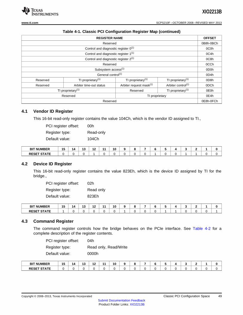
XIO2213B
www.ti.com SCPS210F –OCTOBER 2008–REVISED MAY 2013
Table 4-1. Classic PCI Configuration Register Map (continued)
REGISTER NAME OFFSET
Reserved 0B8h-0BCh
Control and diagnostic register 0(1) 0C0h
Control and diagnostic register 1(1) 0C4h
Control and diagnostic register 2(1) 0C8h
Reserved 0CCh
Subsystem access(1) 0D0h
General control(1) 0D4h
Reserved TI proprietary(1) TI proprietary(1) TI proprietary(1) 0D8h
Reserved Arbiter time-out status Arbiter request mask(1) Arbiter control(1) 0DCh
TI proprietary(1) Reserved TI proprietary(1) 0E0h
Reserved TI proprietary 0E4h
Reserved 0E8h-0FCh
4.1 Vendor ID Register
This 16-bit read-only register contains the value 104Ch, which is the vendor ID assigned to TI.,
PCI register offset: 00h
Register type: Read-only
Default value: 104Ch
BIT NUMBER 15 14 13 12 11 10 9 8 7 6 5 4 3 2 1 0
RESET STATE 0 0 0 1 0 0 0 0 0 1 0 0 1 1 0 0
4.2 Device ID Register
This 16-bit read-only register contains the value 823Eh, which is the device ID assigned by TI for thebridge.,
PCI register offset: 02h
Register type: Read only
Default value: 823Eh
BIT NUMBER 15 14 13 12 11 10 9 8 7 6 5 4 3 2 1 0
RESET STATE 1 0 0 0 0 0 1 0 0 0 1 1 0 0 0 1
4.3 Command Register
The command register controls how the bridge behaves on the PCIe interface. See Table 4-2 for acomplete description of the register contents.
PCI register offset: 04h
Register type: Read only, Read/Write
Default value: 0000h
BIT NUMBER 15 14 13 12 11 10 9 8 7 6 5 4 3 2 1 0
RESET STATE 0 0 0 0 0 0 0 0 0 0 0 0 0 0 0 0
Copyright © 2008–2013, Texas Instruments Incorporated Classic PCI Configuration Space 49Submit Documentation FeedbackProduct Folder Links: XIO2213B
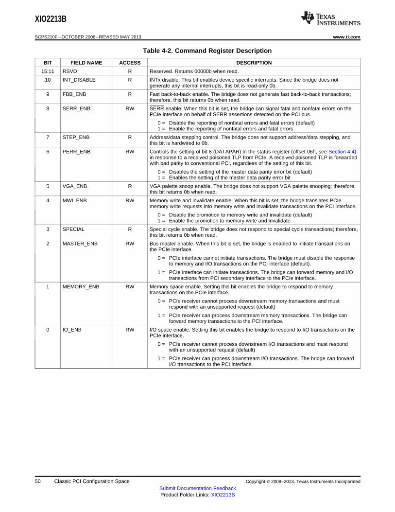
XIO2213B
SCPS210F –OCTOBER 2008–REVISED MAY 2013 www.ti.com
Table 4-2. Command Register Description
BIT FIELD NAME ACCESS DESCRIPTION
15:11 RSVD R Reserved. Returns 00000b when read.
10 INT_DISABLE R INTx disable. This bit enables device specific interrupts. Since the bridge does notgenerate any internal interrupts, this bit is read-only 0b.
9 FBB_ENB R Fast back-to-back enable. The bridge does not generate fast back-to-back transactions;therefore, this bit returns 0b when read.
8 SERR_ENB RW SERR enable. When this bit is set, the bridge can signal fatal and nonfatal errors on thePCIe interface on behalf of SERR assertions detected on the PCI bus.
0 = Disable the reporting of nonfatal errors and fatal errors (default)1 = Enable the reporting of nonfatal errors and fatal errors
7 STEP_ENB R Address/data stepping control. The bridge does not support address/data stepping, andthis bit is hardwired to 0b.
6 PERR_ENB RW Controls the setting of bit 8 (DATAPAR) in the status register (offset 06h, see Section 4.4)in response to a received poisoned TLP from PCIe. A received poisoned TLP is forwardedwith bad parity to conventional PCI, regardless of the setting of this bit.
0 = Disables the setting of the master data parity error bit (default)1 = Enables the setting of the master data parity error bit
5 VGA_ENB R VGA palette snoop enable. The bridge does not support VGA palette snooping; therefore,this bit returns 0b when read.
4 MWI_ENB RW Memory write and invalidate enable. When this bit is set, the bridge translates PCIememory write requests into memory write and invalidate transactions on the PCI interface.
0 = Disable the promotion to memory write and invalidate (default)1 = Enable the promotion to memory write and invalidate
3 SPECIAL R Special cycle enable. The bridge does not respond to special cycle transactions; therefore,this bit returns 0b when read.
2 MASTER_ENB RW Bus master enable. When this bit is set, the bridge is enabled to initiate transactions onthe PCIe interface.
0 = PCIe interface cannot initiate transactions. The bridge must disable the responseto memory and I/O transactions on the PCI interface (default).
1 = PCIe interface can initiate transactions. The bridge can forward memory and I/Otransactions from PCI secondary interface to the PCIe interface.
1 MEMORY_ENB RW Memory space enable. Setting this bit enables the bridge to respond to memorytransactions on the PCIe interface.
0 = PCIe receiver cannot process downstream memory transactions and mustrespond with an unsupported request (default)
1 = PCIe receiver can process downstream memory transactions. The bridge canforward memory transactions to the PCI interface.
0 IO_ENB RW I/O space enable. Setting this bit enables the bridge to respond to I/O transactions on thePCIe interface.
0 = PCIe receiver cannot process downstream I/O transactions and must respondwith an unsupported request (default)
1 = PCIe receiver can process downstream I/O transactions. The bridge can forwardI/O transactions to the PCI interface.
50 Classic PCI Configuration Space Copyright © 2008–2013, Texas Instruments Incorporated
Submit Documentation FeedbackProduct Folder Links: XIO2213B
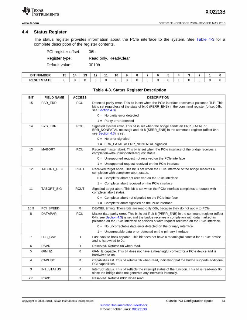
XIO2213B
www.ti.com SCPS210F –OCTOBER 2008–REVISED MAY 2013
4.4 Status Register
The status register provides information about the PCIe interface to the system. See Table 4-3 for acomplete description of the register contents.
PCI register offset: 06h
Register type: Read only, Read/Clear
Default value: 0010h
BIT NUMBER 15 14 13 12 11 10 9 8 7 6 5 4 3 2 1 0
RESET STATE 0 0 0 0 0 0 0 0 0 0 0 1 0 0 0 0
Table 4-3. Status Register Description
BIT FIELD NAME ACCESS DESCRIPTION
15 PAR_ERR RCU Detected parity error. This bit is set when the PCIe interface receives a poisoned TLP. Thisbit is set regardless of the state of bit 6 (PERR_ENB) in the command register (offset 04h,see Section 4.3).
0 = No parity error detected
1 = Parity error detected
14 SYS_ERR RCU Signaled system error. This bit is set when the bridge sends an ERR_FATAL orERR_NONFATAL message and bit 8 (SERR_ENB) in the command register (offset 04h,see Section 4.3) is set.
0 = No error signaled
1 = ERR_FATAL or ERR_NONFATAL signaled
13 MABORT RCU Received master abort. This bit is set when the PCIe interface of the bridge receives acompletion-with-unsupported-request status.
0 = Unsupported request not received on the PCIe interface
1 = Unsupported request received on the PCIe interface
12 TABORT_REC RCUT Received target abort. This bit is set when the PCIe interface of the bridge receives acompletion-with-completer-abort status.
0 = Completer abort not received on the PCIe interface
1 = Completer abort received on the PCIe interface
11 TABORT_SIG RCUT Signaled target abort. This bit is set when the PCIe interface completes a request withcompleter abort status.
0 = Completer abort not signaled on the PCIe interface
1 = Completer abort signaled on the PCIe interface
10:9 PCI_SPEED R DEVSEL timing. These bits are read-only 00b, because they do not apply to PCIe.
8 DATAPAR RCU Master data parity error. This bit is set if bit 6 (PERR_ENB) in the command register (offset04h, see Section 4.3) is set and the bridge receives a completion with data marked aspoisoned on the PCIe interface or poisons a write request received on the PCIe interface.
0 = No uncorrectable data error detected on the primary interface
1 = Uncorrectable data error detected on the primary interface
7 FBB_CAP R Fast back-to-back capable. This bit does not have a meaningful context for a PCIe deviceand is hardwired to 0b.
6 RSVD R Reserved. Returns 0b when read.
5 66MHZ R 66-MHz capable. This bit does not have a meaningful context for a PCIe device and ishardwired to 0b.
4 CAPLIST R Capabilities list. This bit returns 1b when read, indicating that the bridge supports additionalPCI capabilities.
3 INT_STATUS R Interrupt status. This bit reflects the interrupt status of the function. This bit is read-only 0bsince the bridge does not generate any interrupts internally.
2:0 RSVD R Reserved. Returns 000b when read.
Copyright © 2008–2013, Texas Instruments Incorporated Classic PCI Configuration Space 51Submit Documentation FeedbackProduct Folder Links: XIO2213B
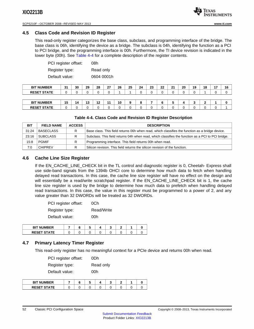
XIO2213B
SCPS210F –OCTOBER 2008–REVISED MAY 2013 www.ti.com
4.5 Class Code and Revision ID Register
This read-only register categorizes the base class, subclass, and programming interface of the bridge. Thebase class is 06h, identifying the device as a bridge. The subclass is 04h, identifying the function as a PCIto PCI bridge, and the programming interface is 00h. Furthermore, the TI device revision is indicated in thelower byte (00h). See Table 4-4 for a complete description of the register contents.
PCI register offset: 08h
Register type: Read only
Default value: 0604 0001h
BIT NUMBER 31 30 29 28 27 26 25 24 23 22 21 20 19 18 17 16
RESET STATE 0 0 0 0 0 1 1 0 0 0 0 0 0 1 0 0
BIT NUMBER 15 14 13 12 11 10 9 8 7 6 5 4 3 2 1 0
RESET STATE 0 0 0 0 0 0 0 0 0 0 0 0 0 0 0 1
Table 4-4. Class Code and Revision ID Register Description
BIT FIELD NAME ACCESS DESCRIPTION
31:24 BASECLASS R Base class. This field returns 06h when read, which classifies the function as a bridge device.
23:16 SUBCLASS R Subclass. This field returns 04h when read, which classifies the function as a PCI to PCI bridge.
15:8 PGMIF R Programming interface. This field returns 00h when read.
7:0 CHIPREV R Silicon revision. This field returns the silicon revision of the function.
4.6 Cache Line Size Register
If the EN_CACHE_LINE_CHECK bit in the TL control and diagnostic register is 0, Cheetah- Express shalluse side-band signals from the 1394b OHCI core to determine how much data to fetch when handlingdelayed read transactions. In this case, the cache line size register will have no effect on the design andwill essentially be a read/write scratchpad register. If the EN_CACHE_LINE_CHECK bit is 1, the cacheline size register is used by the bridge to determine how much data to prefetch when handling delayedread transactions. In this case, the value in this register must be programmed to a power of 2, and anyvalue greater than 32 DWORDs will be treated as 32 DWORDs.
PCI register offset: 0Ch
Register type: Read/Write
Default value: 00h
BIT NUMBER 7 6 5 4 3 2 1 0
RESET STATE 0 0 0 0 0 0 0 0
4.7 Primary Latency Timer Register
This read-only register has no meaningful context for a PCIe device and returns 00h when read.
PCI register offset: 0Dh
Register type: Read only
Default value: 00h
BIT NUMBER 7 6 5 4 3 2 1 0
RESET STATE 0 0 0 0 0 0 0 0
52 Classic PCI Configuration Space Copyright © 2008–2013, Texas Instruments Incorporated
Submit Documentation FeedbackProduct Folder Links: XIO2213B
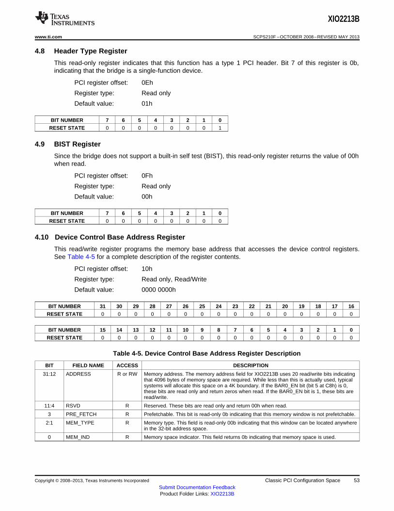
XIO2213B
www.ti.com SCPS210F –OCTOBER 2008–REVISED MAY 2013
4.8 Header Type Register
This read-only register indicates that this function has a type 1 PCI header. Bit 7 of this register is 0b,indicating that the bridge is a single-function device.
PCI register offset: 0Eh
Register type: Read only
Default value: 01h
BIT NUMBER 7 6 5 4 3 2 1 0
RESET STATE 0 0 0 0 0 0 0 1
4.9 BIST Register
Since the bridge does not support a built-in self test (BIST), this read-only register returns the value of 00hwhen read.
PCI register offset: 0Fh
Register type: Read only
Default value: 00h
BIT NUMBER 7 6 5 4 3 2 1 0
RESET STATE 0 0 0 0 0 0 0 0
4.10 Device Control Base Address Register
This read/write register programs the memory base address that accesses the device control registers.See Table 4-5 for a complete description of the register contents.
PCI register offset: 10h
Register type: Read only, Read/Write
Default value: 0000 0000h
BIT NUMBER 31 30 29 28 27 26 25 24 23 22 21 20 19 18 17 16
RESET STATE 0 0 0 0 0 0 0 0 0 0 0 0 0 0 0 0
BIT NUMBER 15 14 13 12 11 10 9 8 7 6 5 4 3 2 1 0
RESET STATE 0 0 0 0 0 0 0 0 0 0 0 0 0 0 0 0
Table 4-5. Device Control Base Address Register Description
BIT FIELD NAME ACCESS DESCRIPTION
31:12 ADDRESS R or RW Memory address. The memory address field for XIO2213B uses 20 read/write bits indicatingthat 4096 bytes of memory space are required. While less than this is actually used, typicalsystems will allocate this space on a 4K boundary. If the BAR0_EN bit (bit 5 at C8h) is 0,these bits are read only and return zeros when read. If the BAR0_EN bit is 1, these bits areread/write.
11:4 RSVD R Reserved. These bits are read only and return 00h when read.
3 PRE_FETCH R Prefetchable. This bit is read-only 0b indicating that this memory window is not prefetchable.
2:1 MEM_TYPE R Memory type. This field is read-only 00b indicating that this window can be located anywherein the 32-bit address space.
0 MEM_IND R Memory space indicator. This field returns 0b indicating that memory space is used.
Copyright © 2008–2013, Texas Instruments Incorporated Classic PCI Configuration Space 53Submit Documentation FeedbackProduct Folder Links: XIO2213B
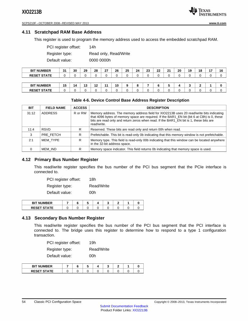
XIO2213B
SCPS210F –OCTOBER 2008–REVISED MAY 2013 www.ti.com
4.11 Scratchpad RAM Base Address
This register is used to program the memory address used to access the embedded scratchpad RAM.
PCI register offset: 14h
Register type: Read only, Read/Write
Default value: 0000 0000h
BIT NUMBER 31 30 29 28 27 26 25 24 23 22 21 20 19 18 17 16
RESET STATE 0 0 0 0 0 0 0 0 0 0 0 0 0 0 0 0
BIT NUMBER 15 14 13 12 11 10 9 8 7 6 5 4 3 2 1 0
RESET STATE 0 0 0 0 0 0 0 0 0 0 0 0 0 0 0 0
Table 4-6. Device Control Base Address Register Description
BIT FIELD NAME ACCESS DESCRIPTION
31:12 ADDRESS R or RW Memory address. The memory address field for XIO2213B uses 20 read/write bits indicatingthat 4096 bytes of memory space are required. If the BAR1_EN bit (bit 6 at C8h) is 0, thesebits are read only and return zeros when read. If the BAR1_EN bit is 1, these bits areread/write.
11:4 RSVD R Reserved. These bits are read only and return 00h when read.
3 PRE_FETCH R Prefetchable. This bit is read-only 0b indicating that this memory window is not prefetchable.
2:1 MEM_TYPE R Memory type. This field is read-only 00b indicating that this window can be located anywherein the 32-bit address space.
0 MEM_IND R Memory space indicator. This field returns 0b indicating that memory space is used.
4.12 Primary Bus Number Register
This read/write register specifies the bus number of the PCI bus segment that the PCIe interface isconnected to.
PCI register offset: 18h
Register type: Read/Write
Default value: 00h
BIT NUMBER 7 6 5 4 3 2 1 0
RESET STATE 0 0 0 0 0 0 0 0
4.13 Secondary Bus Number Register
This read/write register specifies the bus number of the PCI bus segment that the PCI interface isconnected to. The bridge uses this register to determine how to respond to a type 1 configurationtransaction.
PCI register offset: 19h
Register type: Read/Write
Default value: 00h
BIT NUMBER 7 6 5 4 3 2 1 0
RESET STATE 0 0 0 0 0 0 0 0
54 Classic PCI Configuration Space Copyright © 2008–2013, Texas Instruments Incorporated
Submit Documentation FeedbackProduct Folder Links: XIO2213B
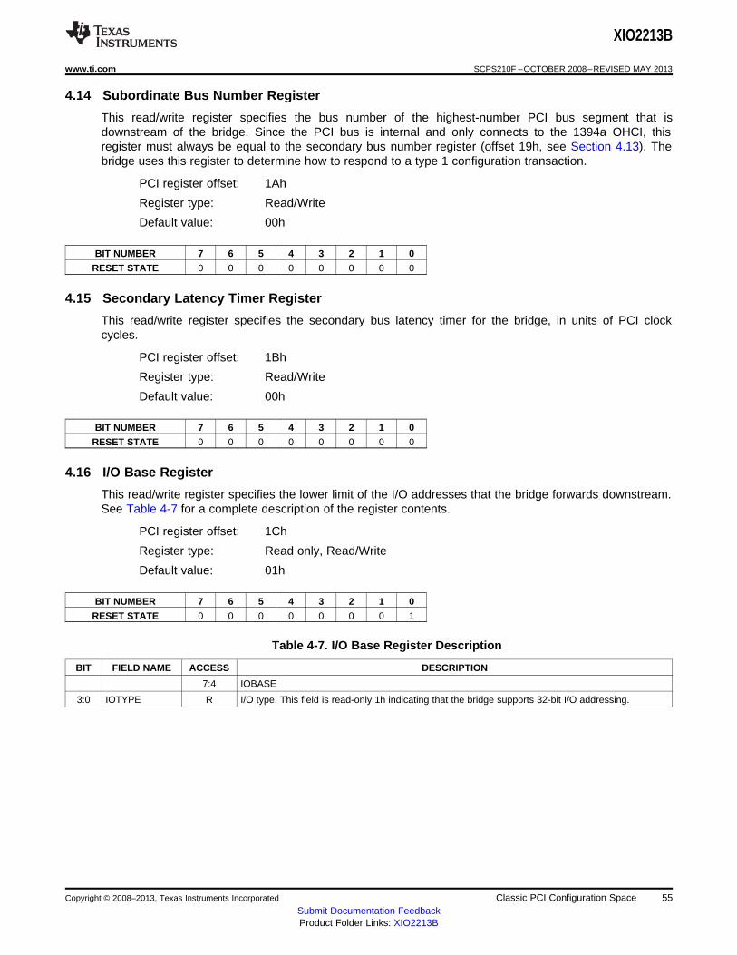
XIO2213B
www.ti.com SCPS210F –OCTOBER 2008–REVISED MAY 2013
4.14 Subordinate Bus Number Register
This read/write register specifies the bus number of the highest-number PCI bus segment that isdownstream of the bridge. Since the PCI bus is internal and only connects to the 1394a OHCI, thisregister must always be equal to the secondary bus number register (offset 19h, see Section 4.13). Thebridge uses this register to determine how to respond to a type 1 configuration transaction.
PCI register offset: 1Ah
Register type: Read/Write
Default value: 00h
BIT NUMBER 7 6 5 4 3 2 1 0
RESET STATE 0 0 0 0 0 0 0 0
4.15 Secondary Latency Timer Register
This read/write register specifies the secondary bus latency timer for the bridge, in units of PCI clockcycles.
PCI register offset: 1Bh
Register type: Read/Write
Default value: 00h
BIT NUMBER 7 6 5 4 3 2 1 0
RESET STATE 0 0 0 0 0 0 0 0
4.16 I/O Base Register
This read/write register specifies the lower limit of the I/O addresses that the bridge forwards downstream.See Table 4-7 for a complete description of the register contents.
PCI register offset: 1Ch
Register type: Read only, Read/Write
Default value: 01h
BIT NUMBER 7 6 5 4 3 2 1 0
RESET STATE 0 0 0 0 0 0 0 1
Table 4-7. I/O Base Register Description
BIT FIELD NAME ACCESS DESCRIPTION
7:4 IOBASE
3:0 IOTYPE R I/O type. This field is read-only 1h indicating that the bridge supports 32-bit I/O addressing.
Copyright © 2008–2013, Texas Instruments Incorporated Classic PCI Configuration Space 55Submit Documentation FeedbackProduct Folder Links: XIO2213B
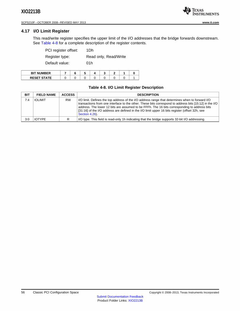
XIO2213B
SCPS210F –OCTOBER 2008–REVISED MAY 2013 www.ti.com
4.17 I/O Limit Register
This read/write register specifies the upper limit of the I/O addresses that the bridge forwards downstream.See Table 4-8 for a complete description of the register contents.
PCI register offset: 1Dh
Register type: Read only, Read/Write
Default value: 01h
BIT NUMBER 7 6 5 4 3 2 1 0
RESET STATE 0 0 0 0 0 0 0 1
Table 4-8. I/O Limit Register Description
BIT FIELD NAME ACCESS DESCRIPTION
7:4 IOLIMIT RW I/O limit. Defines the top address of the I/O address range that determines when to forward I/Otransactions from one interface to the other. These bits correspond to address bits [15:12] in the I/Oaddress. The lower 12 bits are assumed to be FFFh. The 16 bits corresponding to address bits[31:16] of the I/O address are defined in the I/O limit upper 16 bits register (offset 32h, seeSection 4.26).
3:0 IOTYPE R I/O type. This field is read-only 1h indicating that the bridge supports 32-bit I/O addressing.
56 Classic PCI Configuration Space Copyright © 2008–2013, Texas Instruments Incorporated
Submit Documentation FeedbackProduct Folder Links: XIO2213B
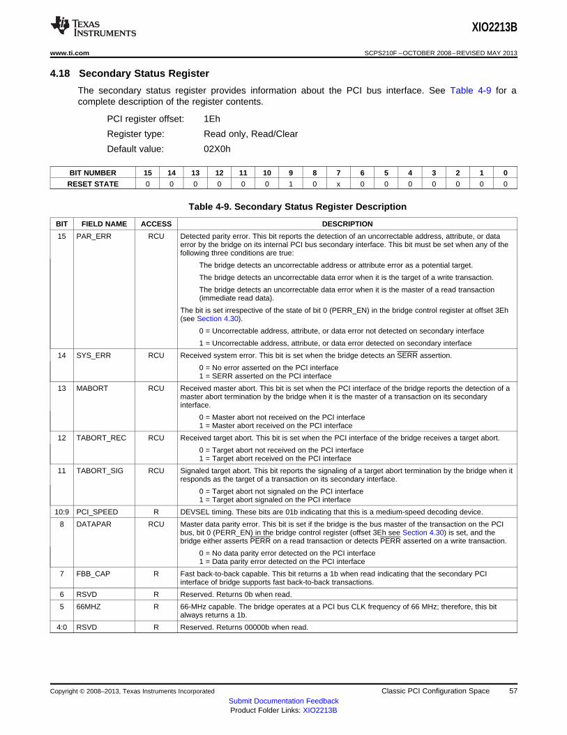
XIO2213B
www.ti.com SCPS210F –OCTOBER 2008–REVISED MAY 2013
4.18 Secondary Status Register
The secondary status register provides information about the PCI bus interface. See Table 4-9 for acomplete description of the register contents.
PCI register offset: 1Eh
Register type: Read only, Read/Clear
Default value: 02X0h
BIT NUMBER 15 14 13 12 11 10 9 8 7 6 5 4 3 2 1 0
RESET STATE 0 0 0 0 0 0 1 0 x 0 0 0 0 0 0 0
Table 4-9. Secondary Status Register Description
BIT FIELD NAME ACCESS DESCRIPTION
15 PAR_ERR RCU Detected parity error. This bit reports the detection of an uncorrectable address, attribute, or dataerror by the bridge on its internal PCI bus secondary interface. This bit must be set when any of thefollowing three conditions are true:
The bridge detects an uncorrectable address or attribute error as a potential target.
The bridge detects an uncorrectable data error when it is the target of a write transaction.
The bridge detects an uncorrectable data error when it is the master of a read transaction(immediate read data).
The bit is set irrespective of the state of bit 0 (PERR_EN) in the bridge control register at offset 3Eh(see Section 4.30).
0 = Uncorrectable address, attribute, or data error not detected on secondary interface
1 = Uncorrectable address, attribute, or data error detected on secondary interface
14 SYS_ERR RCU Received system error. This bit is set when the bridge detects an SERR assertion.
0 = No error asserted on the PCI interface1 = SERR asserted on the PCI interface
13 MABORT RCU Received master abort. This bit is set when the PCI interface of the bridge reports the detection of amaster abort termination by the bridge when it is the master of a transaction on its secondaryinterface.
0 = Master abort not received on the PCI interface1 = Master abort received on the PCI interface
12 TABORT_REC RCU Received target abort. This bit is set when the PCI interface of the bridge receives a target abort.
0 = Target abort not received on the PCI interface1 = Target abort received on the PCI interface
11 TABORT_SIG RCU Signaled target abort. This bit reports the signaling of a target abort termination by the bridge when itresponds as the target of a transaction on its secondary interface.
0 = Target abort not signaled on the PCI interface1 = Target abort signaled on the PCI interface
10:9 PCI_SPEED R DEVSEL timing. These bits are 01b indicating that this is a medium-speed decoding device.
8 DATAPAR RCU Master data parity error. This bit is set if the bridge is the bus master of the transaction on the PCIbus, bit 0 (PERR_EN) in the bridge control register (offset 3Eh see Section 4.30) is set, and thebridge either asserts PERR on a read transaction or detects PERR asserted on a write transaction.
0 = No data parity error detected on the PCI interface1 = Data parity error detected on the PCI interface
7 FBB_CAP R Fast back-to-back capable. This bit returns a 1b when read indicating that the secondary PCIinterface of bridge supports fast back-to-back transactions.
6 RSVD R Reserved. Returns 0b when read.
5 66MHZ R 66-MHz capable. The bridge operates at a PCI bus CLK frequency of 66 MHz; therefore, this bitalways returns a 1b.
4:0 RSVD R Reserved. Returns 00000b when read.
Copyright © 2008–2013, Texas Instruments Incorporated Classic PCI Configuration Space 57Submit Documentation FeedbackProduct Folder Links: XIO2213B
XIO2213B
SCPS210F –OCTOBER 2008–REVISED MAY 2013 www.ti.com
4.19 Memory Base Register
This read/write register specifies the lower limit of the memory addresses that the bridge forwardsdownstream. See Table 4-10 for a complete description of the register contents.
PCI register offset: 20h
Register type: Read only, Read/Write
Default value: 0000h
BIT NUMBER 15 14 13 12 11 10 9 8 7 6 5 4 3 2 1 0
RESET STATE 0 0 0 0 0 0 0 0 0 0 0 0 0 0 0 0
Table 4-10. Memory Base Register Description
BIT FIELD NAME ACCESS DESCRIPTION
15:4 MEMBASE RW Memory base. Defines the lowest address of the memory address range that determines when toforward memory transactions from one interface to the other. These bits correspond to address bits[31:20] in the memory address. The lower 20 bits are assumed to be 00000h.
3:0 RSVD R Reserved. Returns 0h when read.
4.20 Memory Limit Register
This read/write register specifies the upper limit of the memory addresses that the bridge forwardsdownstream. See Table 4-11 for a complete description of the register contents.
PCI register offset: 22h
Register type: Read only, Read/Write
Default value: 0000h
BIT NUMBER 15 14 13 12 11 10 9 8 7 6 5 4 3 2 1 0
RESET STATE 0 0 0 0 0 0 0 0 0 0 0 0 0 0 0 0
Table 4-11. Memory Limit Register Description
BIT FIELD NAME ACCESS DESCRIPTION
15:4 MEMLIMIT RW Memory limit. Defines the highest address of the memory address range that determines when toforward memory transactions from one interface to the other. These bits correspond to address bits[31:20] in the memory address. The lower 20 bits are assumed to be FFFFFh.
3:0 RSVD R Reserved. Returns 0h when read.
58 Classic PCI Configuration Space Copyright © 2008–2013, Texas Instruments Incorporated
Submit Documentation FeedbackProduct Folder Links: XIO2213B
XIO2213B
www.ti.com SCPS210F –OCTOBER 2008–REVISED MAY 2013
4.21 Prefetchable Memory Base Register
This read/write register specifies the lower limit of the prefetchable memory addresses that the bridgeforwards downstream. See Table 4-12 for a complete description of the register contents.
PCI register offset: 24h
Register type: Read only, Read/Write
Default value: 0001h
BIT NUMBER 15 14 13 12 11 10 9 8 7 6 5 4 3 2 1 0
RESET STATE 0 0 0 0 0 0 0 0 0 0 0 0 0 0 0 1
Table 4-12. Prefetchable Memory Base Register Description
BIT FIELD NAME ACCESS DESCRIPTION
15:4 PREBASE RW Prefetchable memory base. Defines the lowest address of the prefetchable memory address rangethat determines when to forward memory transactions from one interface to the other. These bitscorrespond to address bits [31:20] in the memory address. The lower 20 bits are assumed to be00000h. The prefetchable base upper 32 bits register (offset 28h, see Section 4.23) specifies the bit[63:32] of the 64-bit prefetchable memory address.
3:0 64BIT R 64-bit memory indicator. These read-only bits indicate that 64-bit addressing is supported for thismemory window.
4.22 Prefetchable Memory Limit Register
This read/write register specifies the upper limit of the prefetchable memory addresses that the bridgeforwards downstream. See Table 4-13 for a complete description of the register contents.
PCI register offset: 26h
Register type: Read only, Read/Write
Default value: 0001h
BIT NUMBER 15 14 13 12 11 10 9 8 7 6 5 4 3 2 1 0
RESET STATE 0 0 0 0 0 0 0 0 0 0 0 0 0 0 0 1
Table 4-13. Prefetchable Memory Limit Register Description
BIT FIELD NAME ACCESS DESCRIPTION
15:4 PRELIMIT RW Prefetchable memory limit. Defines the highest address of the prefetchable memory address rangethat determines when to forward memory transactions from one interface to the other. These bitscorrespond to address bits [31:20] in the memory address. The lower 20 bits are assumed to beFFFFFh. The prefetchable limit upper 32 bits register (offset 2Ch, see Section 4.24) specifies the bit[63:32] of the 64-bit prefetchable memory address.
3:0 64BIT R 64-bit memory indicator. These read-only bits indicate that 64-bit addressing is supported for thismemory window.
Copyright © 2008–2013, Texas Instruments Incorporated Classic PCI Configuration Space 59Submit Documentation FeedbackProduct Folder Links: XIO2213B
XIO2213B
SCPS210F –OCTOBER 2008–REVISED MAY 2013 www.ti.com
4.23 Prefetchable Base Upper 32 Bits Register
This read/write register specifies the upper 32 bits of the prefetchable memory base register. See Table 4-14 for a complete description of the register contents.
PCI register offset: 28h
Register type: Read/Write
Default value: 0000 0000h
BIT NUMBER 31 30 29 28 27 26 25 24 23 22 21 20 19 18 17 16
RESET STATE 0 0 0 0 0 0 0 0 0 0 0 0 0 0 0 0
BIT NUMBER 15 14 13 12 11 10 9 8 7 6 5 4 3 2 1 0
RESET STATE 0 0 0 0 0 0 0 0 0 0 0 0 0 0 0 0
Table 4-14. Prefetchable Base Upper 32 Bits Register Description
BIT FIELD NAME ACCESS DESCRIPTION
31:0 PREBASE RW Prefetchable memory base upper 32 bits. Defines the upper 32 bits of the lowest address of theprefetchable memory address range that determines when to forward memory transactionsdownstream.
4.24 Prefetchable Limit Upper 32 Bits Register
This read/write register specifies the upper 32 bits of the prefetchable memory limit register. See Table 4-15 for a complete description of the register contents.
PCI register offset: 2Ch
Register type: Read/Write
Default value: 0000 0000h
BIT NUMBER 31 30 29 28 27 26 25 24 23 22 21 20 19 18 17 16
RESET STATE 0 0 0 0 0 0 0 0 0 0 0 0 0 0 0 0
BIT NUMBER 15 14 13 12 11 10 9 8 7 6 5 4 3 2 1 0
RESET STATE 0 0 0 0 0 0 0 0 0 0 0 0 0 0 0 0
Table 4-15. Prefetchable Limit Upper 32 Bits Register Description
BIT FIELD NAME ACCESS DESCRIPTION
31:0 PRELIMIT RW Prefetchable memory limit upper 32 bits. Defines the upper 32 bits of the highest address of theprefetchable memory address range that determines when to forward memory transactionsdownstream.
60 Classic PCI Configuration Space Copyright © 2008–2013, Texas Instruments Incorporated
Submit Documentation FeedbackProduct Folder Links: XIO2213B
XIO2213B
www.ti.com SCPS210F –OCTOBER 2008–REVISED MAY 2013
4.25 I/O Base Upper 16 Bits Register
This read/write register specifies the upper 16 bits of the I/O base register. See Table 4-16 for a completedescription of the register contents.
PCI register offset: 30h
Register type: Read/Write
Default value: 0000h
BIT NUMBER 15 14 13 12 11 10 9 8 7 6 5 4 3 2 1 0
RESET STATE 0 0 0 0 0 0 0 0 0 0 0 0 0 0 0 0
Table 4-16. I/O Base Upper 16 Bits Register Description
BIT FIELD NAME ACCESS DESCRIPTION
15:0 IOBASE RW I/O base upper 16 bits. Defines the upper 16 bits of the lowest address of the I/O address rangethat determines when to forward I/O transactions downstream. These bits correspond to addressbits [31:20] in the I/O address. The lower 20 bits are assumed to be 00000h.
4.26 I/O Limit Upper 16 Bits Register
This read/write register specifies the upper 16 bits of the I/O limit register. See Table 4-17 for a completedescription of the register contents.
PCI register offset: 32h
Register type: Read/Write
Default value: 0000h
BIT NUMBER 15 14 13 12 11 10 9 8 7 6 5 4 3 2 1 0
RESET STATE 0 0 0 0 0 0 0 0 0 0 0 0 0 0 0 0
Table 4-17. I/O Limit Upper 16 Bits Register Description
BIT FIELD NAME ACCESS DESCRIPTION
15:0 IOLIMIT RW I/O limit upper 16 bits. Defines the upper 16 bits of the top address of the I/O address range thatdetermines when to forward I/O transactions downstream. These bits correspond to address bits[31:20] in the I/O address. The lower 20 bits are assumed to be FFFFFh.
Copyright © 2008–2013, Texas Instruments Incorporated Classic PCI Configuration Space 61Submit Documentation FeedbackProduct Folder Links: XIO2213B
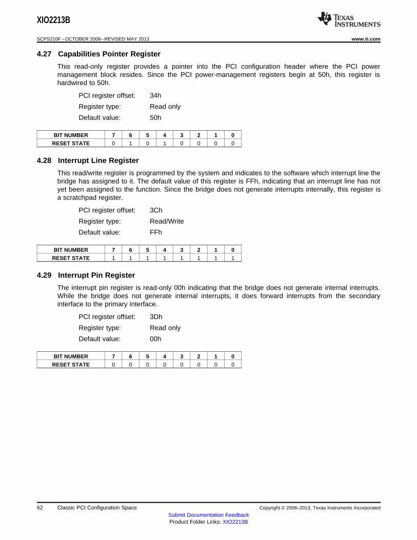
XIO2213B
SCPS210F –OCTOBER 2008–REVISED MAY 2013 www.ti.com
4.27 Capabilities Pointer Register
This read-only register provides a pointer into the PCI configuration header where the PCI powermanagement block resides. Since the PCI power-management registers begin at 50h, this register ishardwired to 50h.
PCI register offset: 34h
Register type: Read only
Default value: 50h
BIT NUMBER 7 6 5 4 3 2 1 0
RESET STATE 0 1 0 1 0 0 0 0
4.28 Interrupt Line Register
This read/write register is programmed by the system and indicates to the software which interrupt line thebridge has assigned to it. The default value of this register is FFh, indicating that an interrupt line has notyet been assigned to the function. Since the bridge does not generate interrupts internally, this register isa scratchpad register.
PCI register offset: 3Ch
Register type: Read/Write
Default value: FFh
BIT NUMBER 7 6 5 4 3 2 1 0
RESET STATE 1 1 1 1 1 1 1 1
4.29 Interrupt Pin Register
The interrupt pin register is read-only 00h indicating that the bridge does not generate internal interrupts.While the bridge does not generate internal interrupts, it does forward interrupts from the secondaryinterface to the primary interface.
PCI register offset: 3Dh
Register type: Read only
Default value: 00h
BIT NUMBER 7 6 5 4 3 2 1 0
RESET STATE 0 0 0 0 0 0 0 0
62 Classic PCI Configuration Space Copyright © 2008–2013, Texas Instruments Incorporated
Submit Documentation FeedbackProduct Folder Links: XIO2213B
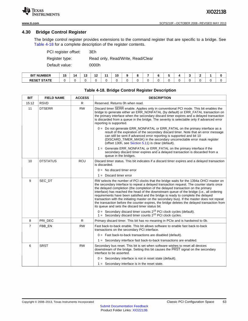
XIO2213B
www.ti.com SCPS210F –OCTOBER 2008–REVISED MAY 2013
4.30 Bridge Control Register
The bridge control register provides extensions to the command register that are specific to a bridge. SeeTable 4-18 for a complete description of the register contents.
PCI register offset: 3Eh
Register type: Read only, Read/Write, Read/Clear
Default value: 0000h
BIT NUMBER 15 14 13 12 11 10 9 8 7 6 5 4 3 2 1 0
RESET STATE 0 0 0 0 0 0 0 0 0 0 0 0 0 0 0 0
Table 4-18. Bridge Control Register Description
BIT FIELD NAME ACCESS DESCRIPTION
15:12 RSVD R Reserved. Returns 0h when read.
11 DTSERR RW Discard timer SERR enable. Applies only in conventional PCI mode. This bit enables thebridge to generate either an ERR_NONFATAL (by default) or ERR_FATAL transaction onthe primary interface when the secondary discard timer expires and a delayed transactionis discarded from a queue in the bridge. The severity is selectable only if advanced errorreporting is supported.
0 = Do not generate ERR_NONFATAL or ERR_FATAL on the primary interface as aresult of the expiration of the secondary discard timer. Note that an error messagecan still be sent if advanced error reporting is supported and bit 10(DISCARD_TIMER_MASK) in the secondary uncorrectable error mask register(offset 130h, see Section 5.11) is clear (default).
1 = Generate ERR_NONFATAL or ERR_FATAL on the primary interface if thesecondary discard timer expires and a delayed transaction is discarded from aqueue in the bridges.
10 DTSTATUS RCU Discard timer status. This bit indicates if a discard timer expires and a delayed transactionis discarded.
0 = No discard timer error
1 = Discard timer error
9 SEC_DT RW selects the number of PCI clocks that the bridge waits for the 1394a OHCI master onthe secondary interface to repeat a delayed transaction request. The counter starts oncethe delayed completion (the completion of the delayed transaction on the primaryinterface) has reached the head of the downstream queue of the bridge (i.e., all orderingrequirements have been satisfied and the bridge is ready to complete the delayedtransaction with the initiating master on the secondary bus). If the master does not repeatthe transaction before the counter expires, the bridge deletes the delayed transaction fromits queue and sets the discard timer status bit.
0 = Secondary discard timer counts 215 PCI clock cycles (default).1 = Secondary discard timer counts 210 PCI clock cycles.
8 PRI_DEC R Primary discard timer. This bit has no meaning in PCIe and is hardwired to 0b.
7 FBB_EN RW Fast back-to-back enable. This bit allows software to enable fast back-to-backtransactions on the secondary PCI interface.
0 = Fast back-to-back transactions are disabled (default).
1 = Secondary interface fast back-to-back transactions are enabled.
6 SRST RW Secondary bus reset. This bit is set when software wishes to reset all devicesdownstream of the bridge. Setting this bit causes the PRST signal on the secondaryinterface to be asserted.
0 = Secondary interface is not in reset state (default).
1 = Secondary interface is in the reset state.
Copyright © 2008–2013, Texas Instruments Incorporated Classic PCI Configuration Space 63Submit Documentation FeedbackProduct Folder Links: XIO2213B
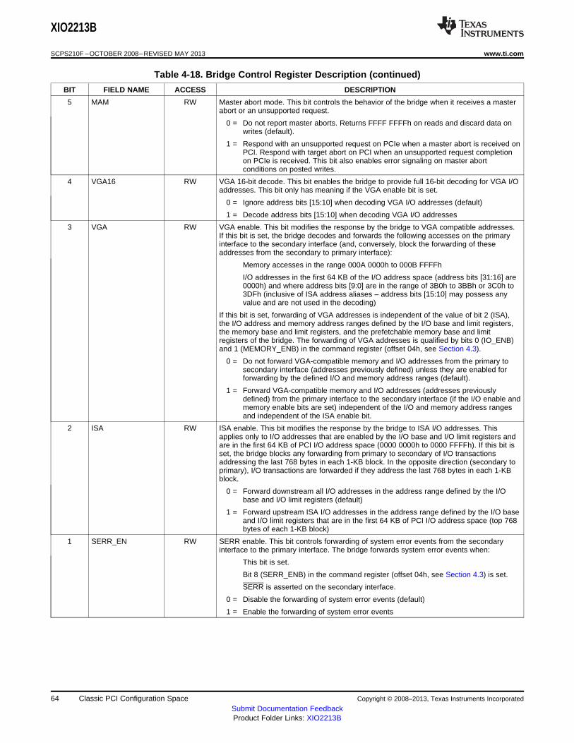
XIO2213B
SCPS210F –OCTOBER 2008–REVISED MAY 2013 www.ti.com
Table 4-18. Bridge Control Register Description (continued)
BIT FIELD NAME ACCESS DESCRIPTION
5 MAM RW Master abort mode. This bit controls the behavior of the bridge when it receives a masterabort or an unsupported request.
0 = Do not report master aborts. Returns FFFF FFFFh on reads and discard data onwrites (default).
1 = Respond with an unsupported request on PCIe when a master abort is received onPCI. Respond with target abort on PCI when an unsupported request completionon PCIe is received. This bit also enables error signaling on master abortconditions on posted writes.
4 VGA16 RW VGA 16-bit decode. This bit enables the bridge to provide full 16-bit decoding for VGA I/Oaddresses. This bit only has meaning if the VGA enable bit is set.
0 = Ignore address bits [15:10] when decoding VGA I/O addresses (default)
1 = Decode address bits [15:10] when decoding VGA I/O addresses
3 VGA RW VGA enable. This bit modifies the response by the bridge to VGA compatible addresses.If this bit is set, the bridge decodes and forwards the following accesses on the primaryinterface to the secondary interface (and, conversely, block the forwarding of theseaddresses from the secondary to primary interface):
Memory accesses in the range 000A 0000h to 000B FFFFh
I/O addresses in the first 64 KB of the I/O address space (address bits [31:16] are0000h) and where address bits [9:0] are in the range of 3B0h to 3BBh or 3C0h to3DFh (inclusive of ISA address aliases – address bits [15:10] may possess anyvalue and are not used in the decoding)
If this bit is set, forwarding of VGA addresses is independent of the value of bit 2 (ISA),the I/O address and memory address ranges defined by the I/O base and limit registers,the memory base and limit registers, and the prefetchable memory base and limitregisters of the bridge. The forwarding of VGA addresses is qualified by bits 0 (IO_ENB)and 1 (MEMORY_ENB) in the command register (offset 04h, see Section 4.3).
0 = Do not forward VGA-compatible memory and I/O addresses from the primary tosecondary interface (addresses previously defined) unless they are enabled forforwarding by the defined I/O and memory address ranges (default).
1 = Forward VGA-compatible memory and I/O addresses (addresses previouslydefined) from the primary interface to the secondary interface (if the I/O enable andmemory enable bits are set) independent of the I/O and memory address rangesand independent of the ISA enable bit.
2 ISA RW ISA enable. This bit modifies the response by the bridge to ISA I/O addresses. Thisapplies only to I/O addresses that are enabled by the I/O base and I/O limit registers andare in the first 64 KB of PCI I/O address space (0000 0000h to 0000 FFFFh). If this bit isset, the bridge blocks any forwarding from primary to secondary of I/O transactionsaddressing the last 768 bytes in each 1-KB block. In the opposite direction (secondary toprimary), I/O transactions are forwarded if they address the last 768 bytes in each 1-KBblock.
0 = Forward downstream all I/O addresses in the address range defined by the I/Obase and I/O limit registers (default)
1 = Forward upstream ISA I/O addresses in the address range defined by the I/O baseand I/O limit registers that are in the first 64 KB of PCI I/O address space (top 768bytes of each 1-KB block)
1 SERR_EN RW SERR enable. This bit controls forwarding of system error events from the secondaryinterface to the primary interface. The bridge forwards system error events when:
This bit is set.
Bit 8 (SERR_ENB) in the command register (offset 04h, see Section 4.3) is set.
SERR is asserted on the secondary interface.
0 = Disable the forwarding of system error events (default)
1 = Enable the forwarding of system error events
64 Classic PCI Configuration Space Copyright © 2008–2013, Texas Instruments Incorporated
Submit Documentation FeedbackProduct Folder Links: XIO2213B
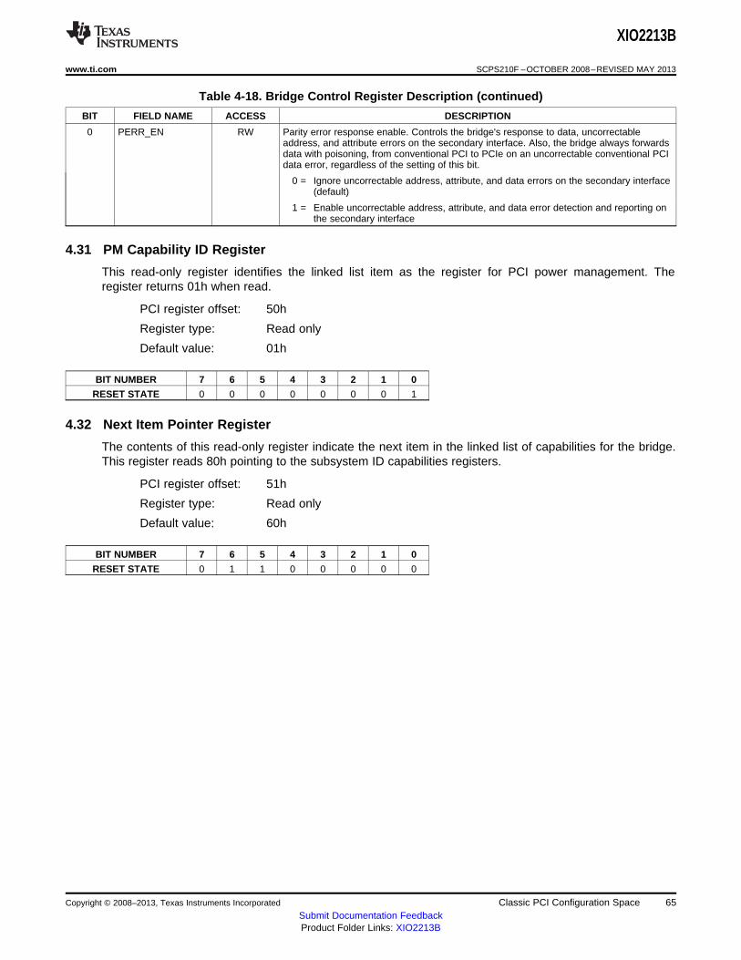
XIO2213B
www.ti.com SCPS210F –OCTOBER 2008–REVISED MAY 2013
Table 4-18. Bridge Control Register Description (continued)
BIT FIELD NAME ACCESS DESCRIPTION
0 PERR_EN RW Parity error response enable. Controls the bridge's response to data, uncorrectableaddress, and attribute errors on the secondary interface. Also, the bridge always forwardsdata with poisoning, from conventional PCI to PCIe on an uncorrectable conventional PCIdata error, regardless of the setting of this bit.
0 = Ignore uncorrectable address, attribute, and data errors on the secondary interface(default)
1 = Enable uncorrectable address, attribute, and data error detection and reporting onthe secondary interface
4.31 PM Capability ID Register
This read-only register identifies the linked list item as the register for PCI power management. Theregister returns 01h when read.
PCI register offset: 50h
Register type: Read only
Default value: 01h
BIT NUMBER 7 6 5 4 3 2 1 0
RESET STATE 0 0 0 0 0 0 0 1
4.32 Next Item Pointer Register
The contents of this read-only register indicate the next item in the linked list of capabilities for the bridge.This register reads 80h pointing to the subsystem ID capabilities registers.
PCI register offset: 51h
Register type: Read only
Default value: 60h
BIT NUMBER 7 6 5 4 3 2 1 0
RESET STATE 0 1 1 0 0 0 0 0
Copyright © 2008–2013, Texas Instruments Incorporated Classic PCI Configuration Space 65Submit Documentation FeedbackProduct Folder Links: XIO2213B
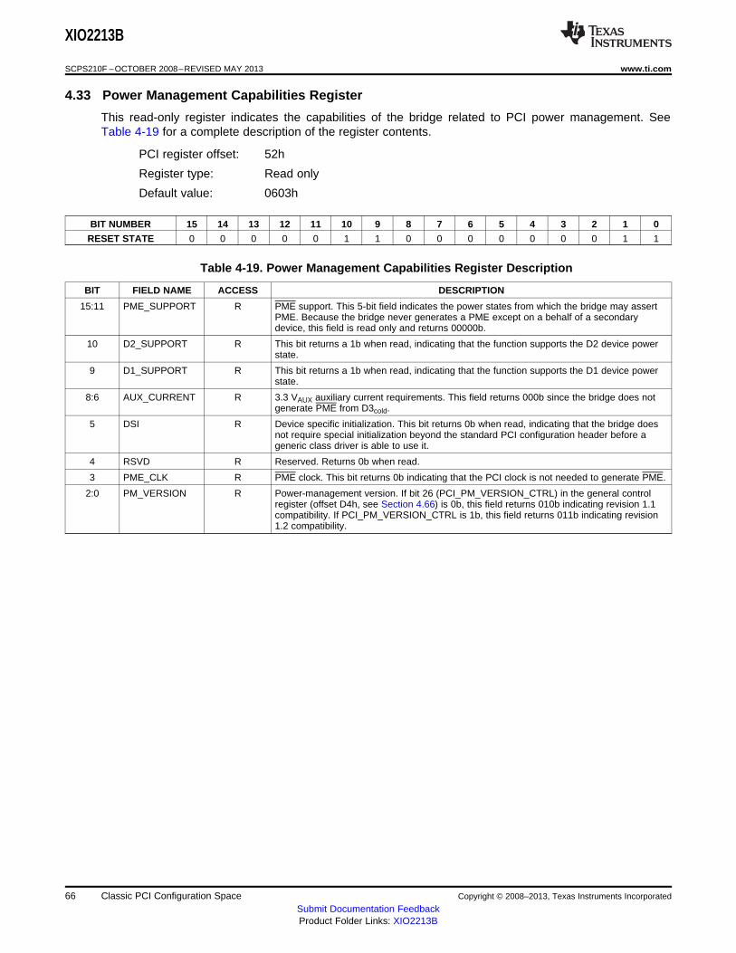
XIO2213B
SCPS210F –OCTOBER 2008–REVISED MAY 2013 www.ti.com
4.33 Power Management Capabilities Register
This read-only register indicates the capabilities of the bridge related to PCI power management. SeeTable 4-19 for a complete description of the register contents.
PCI register offset: 52h
Register type: Read only
Default value: 0603h
BIT NUMBER 15 14 13 12 11 10 9 8 7 6 5 4 3 2 1 0
RESET STATE 0 0 0 0 0 1 1 0 0 0 0 0 0 0 1 1
Table 4-19. Power Management Capabilities Register Description
BIT FIELD NAME ACCESS DESCRIPTION
15:11 PME_SUPPORT R PME support. This 5-bit field indicates the power states from which the bridge may assertPME. Because the bridge never generates a PME except on a behalf of a secondarydevice, this field is read only and returns 00000b.
10 D2_SUPPORT R This bit returns a 1b when read, indicating that the function supports the D2 device powerstate.
9 D1_SUPPORT R This bit returns a 1b when read, indicating that the function supports the D1 device powerstate.
8:6 AUX_CURRENT R 3.3 VAUX auxiliary current requirements. This field returns 000b since the bridge does notgenerate PME from D3cold.
5 DSI R Device specific initialization. This bit returns 0b when read, indicating that the bridge doesnot require special initialization beyond the standard PCI configuration header before ageneric class driver is able to use it.
4 RSVD R Reserved. Returns 0b when read.
3 PME_CLK R PME clock. This bit returns 0b indicating that the PCI clock is not needed to generate PME.
2:0 PM_VERSION R Power-management version. If bit 26 (PCI_PM_VERSION_CTRL) in the general controlregister (offset D4h, see Section 4.66) is 0b, this field returns 010b indicating revision 1.1compatibility. If PCI_PM_VERSION_CTRL is 1b, this field returns 011b indicating revision1.2 compatibility.
66 Classic PCI Configuration Space Copyright © 2008–2013, Texas Instruments Incorporated
Submit Documentation FeedbackProduct Folder Links: XIO2213B
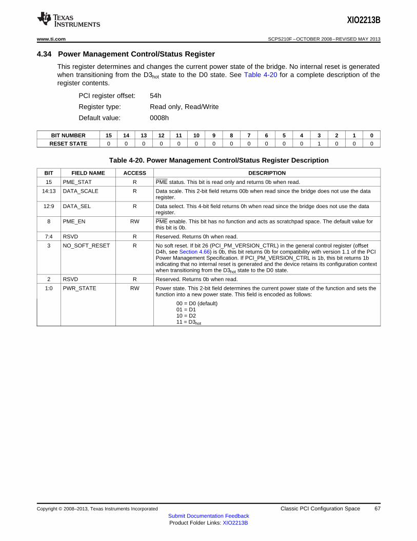
XIO2213B
www.ti.com SCPS210F –OCTOBER 2008–REVISED MAY 2013
4.34 Power Management Control/Status Register
This register determines and changes the current power state of the bridge. No internal reset is generatedwhen transitioning from the D3hot state to the D0 state. See Table 4-20 for a complete description of theregister contents.
PCI register offset: 54h
Register type: Read only, Read/Write
Default value: 0008h
BIT NUMBER 15 14 13 12 11 10 9 8 7 6 5 4 3 2 1 0
RESET STATE 0 0 0 0 0 0 0 0 0 0 0 0 1 0 0 0
Table 4-20. Power Management Control/Status Register Description
BIT FIELD NAME ACCESS DESCRIPTION
15 PME_STAT R PME status. This bit is read only and returns 0b when read.
14:13 DATA_SCALE R Data scale. This 2-bit field returns 00b when read since the bridge does not use the dataregister.
12:9 DATA_SEL R Data select. This 4-bit field returns 0h when read since the bridge does not use the dataregister.
8 PME_EN RW PME enable. This bit has no function and acts as scratchpad space. The default value forthis bit is 0b.
7:4 RSVD R Reserved. Returns 0h when read.
3 NO_SOFT_RESET R No soft reset. If bit 26 (PCI_PM_VERSION_CTRL) in the general control register (offsetD4h, see Section 4.66) is 0b, this bit returns 0b for compatibility with version 1.1 of the PCIPower Management Specification. If PCI_PM_VERSION_CTRL is 1b, this bit returns 1bindicating that no internal reset is generated and the device retains its configuration contextwhen transitioning from the D3hot state to the D0 state.
2 RSVD R Reserved. Returns 0b when read.
1:0 PWR_STATE RW Power state. This 2-bit field determines the current power state of the function and sets thefunction into a new power state. This field is encoded as follows:
00 = D0 (default)01 = D110 = D211 = D3hot
Copyright © 2008–2013, Texas Instruments Incorporated Classic PCI Configuration Space 67Submit Documentation FeedbackProduct Folder Links: XIO2213B
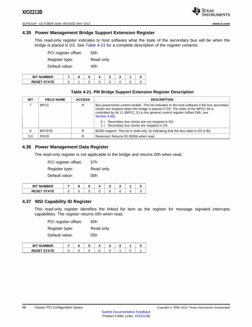
XIO2213B
SCPS210F –OCTOBER 2008–REVISED MAY 2013 www.ti.com
4.35 Power Management Bridge Support Extension Register
This read-only register indicates to host software what the state of the secondary bus will be when thebridge is placed in D3. See Table 4-21 for a complete description of the register contents.
PCI register offset: 56h
Register type: Read only
Default value: 40h
BIT NUMBER 7 6 5 4 3 2 1 0
RESET STATE 0 1 0 0 0 0 0 0
Table 4-21. PM Bridge Support Extension Register Description
BIT FIELD NAME ACCESS DESCRIPTION
7 BPCC R Bus power/clock control enable. This bit indicates to the host software if the bus secondaryclocks are stopped when the bridge is placed in D3. The state of the BPCC bit iscontrolled by bit 11 (BPCC_E) in the general control register (offset D4h, seeSection 4.66).
0 = Secondary bus clocks are not stopped in D3.1 = Secondary bus clocks are stopped in D3.
6 BSTATE R B2/B3 support. This bit is read-only 1b indicating that the bus state in D3 is B2.
5:0 RSVD R Reserved. Returns 00 0000b when read.
4.36 Power Management Data Register
The read-only register is not applicable to the bridge and returns 00h when read.
PCI register offset: 57h
Register type: Read only
Default value: 00h
BIT NUMBER 7 6 5 4 3 2 1 0
RESET STATE 0 0 0 0 0 0 0 0
4.37 MSI Capability ID Register
This read-only register identifies the linked list item as the register for message signaled interruptscapabilities. The register returns 05h when read.
PCI register offset: 60h
Register type: Read only
Default value: 05h
BIT NUMBER 7 6 5 4 3 2 1 0
RESET STATE 0 0 0 0 0 1 0 1
68 Classic PCI Configuration Space Copyright © 2008–2013, Texas Instruments Incorporated
Submit Documentation FeedbackProduct Folder Links: XIO2213B
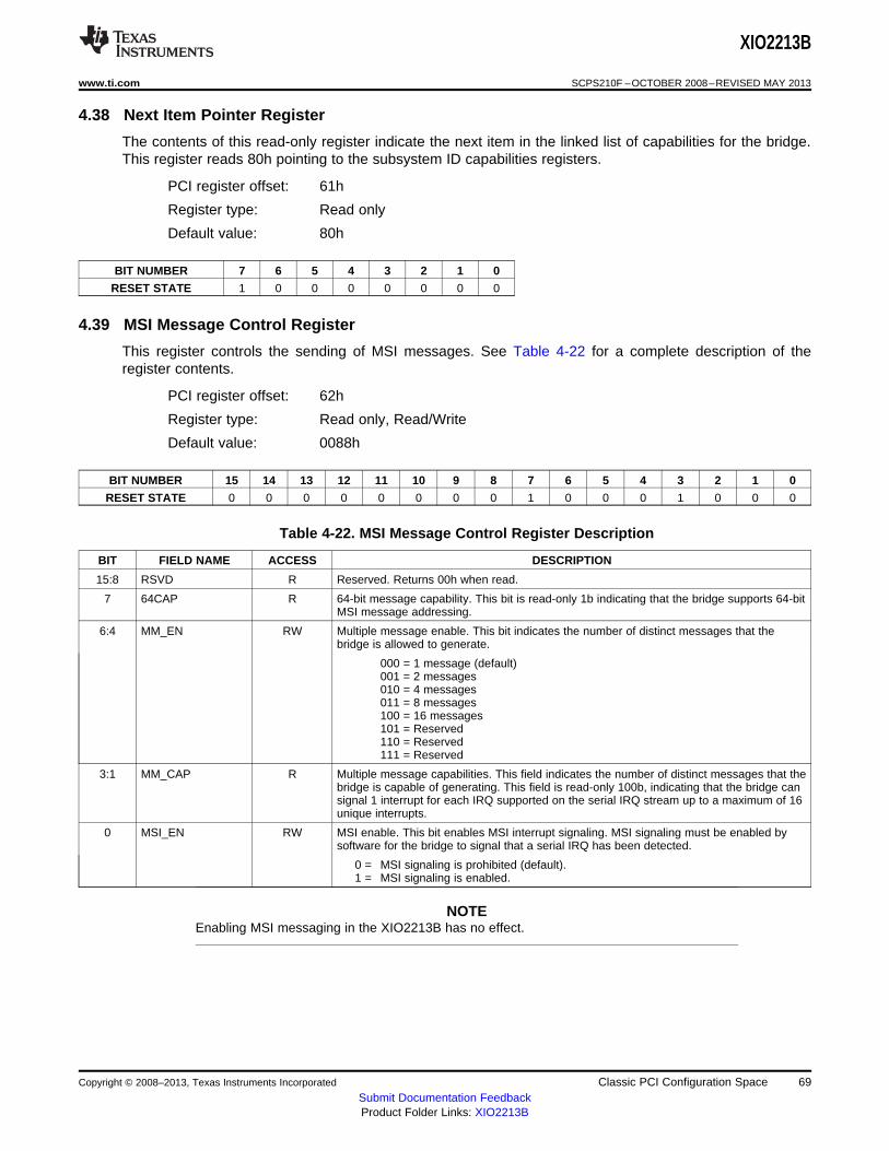
XIO2213B
www.ti.com SCPS210F –OCTOBER 2008–REVISED MAY 2013
4.38 Next Item Pointer Register
The contents of this read-only register indicate the next item in the linked list of capabilities for the bridge.This register reads 80h pointing to the subsystem ID capabilities registers.
PCI register offset: 61h
Register type: Read only
Default value: 80h
BIT NUMBER 7 6 5 4 3 2 1 0
RESET STATE 1 0 0 0 0 0 0 0
4.39 MSI Message Control Register
This register controls the sending of MSI messages. See Table 4-22 for a complete description of theregister contents.
PCI register offset: 62h
Register type: Read only, Read/Write
Default value: 0088h
BIT NUMBER 15 14 13 12 11 10 9 8 7 6 5 4 3 2 1 0
RESET STATE 0 0 0 0 0 0 0 0 1 0 0 0 1 0 0 0
Table 4-22. MSI Message Control Register Description
BIT FIELD NAME ACCESS DESCRIPTION
15:8 RSVD R Reserved. Returns 00h when read.
7 64CAP R 64-bit message capability. This bit is read-only 1b indicating that the bridge supports 64-bitMSI message addressing.
6:4 MM_EN RW Multiple message enable. This bit indicates the number of distinct messages that thebridge is allowed to generate.
000 = 1 message (default)001 = 2 messages010 = 4 messages011 = 8 messages100 = 16 messages101 = Reserved110 = Reserved111 = Reserved
3:1 MM_CAP R Multiple message capabilities. This field indicates the number of distinct messages that thebridge is capable of generating. This field is read-only 100b, indicating that the bridge cansignal 1 interrupt for each IRQ supported on the serial IRQ stream up to a maximum of 16unique interrupts.
0 MSI_EN RW MSI enable. This bit enables MSI interrupt signaling. MSI signaling must be enabled bysoftware for the bridge to signal that a serial IRQ has been detected.
0 = MSI signaling is prohibited (default).1 = MSI signaling is enabled.
NOTEEnabling MSI messaging in the XIO2213B has no effect.
Copyright © 2008–2013, Texas Instruments Incorporated Classic PCI Configuration Space 69Submit Documentation FeedbackProduct Folder Links: XIO2213B
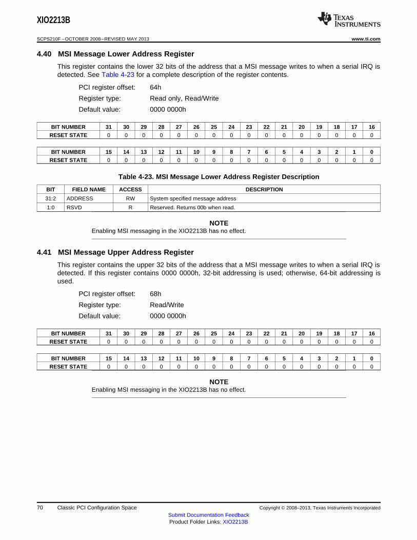
XIO2213B
SCPS210F –OCTOBER 2008–REVISED MAY 2013 www.ti.com
4.40 MSI Message Lower Address Register
This register contains the lower 32 bits of the address that a MSI message writes to when a serial IRQ isdetected. See Table 4-23 for a complete description of the register contents.
PCI register offset: 64h
Register type: Read only, Read/Write
Default value: 0000 0000h
BIT NUMBER 31 30 29 28 27 26 25 24 23 22 21 20 19 18 17 16
RESET STATE 0 0 0 0 0 0 0 0 0 0 0 0 0 0 0 0
BIT NUMBER 15 14 13 12 11 10 9 8 7 6 5 4 3 2 1 0
RESET STATE 0 0 0 0 0 0 0 0 0 0 0 0 0 0 0 0
Table 4-23. MSI Message Lower Address Register Description
BIT FIELD NAME ACCESS DESCRIPTION
31:2 ADDRESS RW System specified message address
1:0 RSVD R Reserved. Returns 00b when read.
NOTEEnabling MSI messaging in the XIO2213B has no effect.
4.41 MSI Message Upper Address Register
This register contains the upper 32 bits of the address that a MSI message writes to when a serial IRQ isdetected. If this register contains 0000 0000h, 32-bit addressing is used; otherwise, 64-bit addressing isused.
PCI register offset: 68h
Register type: Read/Write
Default value: 0000 0000h
BIT NUMBER 31 30 29 28 27 26 25 24 23 22 21 20 19 18 17 16
RESET STATE 0 0 0 0 0 0 0 0 0 0 0 0 0 0 0 0
BIT NUMBER 15 14 13 12 11 10 9 8 7 6 5 4 3 2 1 0
RESET STATE 0 0 0 0 0 0 0 0 0 0 0 0 0 0 0 0
NOTEEnabling MSI messaging in the XIO2213B has no effect.
70 Classic PCI Configuration Space Copyright © 2008–2013, Texas Instruments Incorporated
Submit Documentation FeedbackProduct Folder Links: XIO2213B
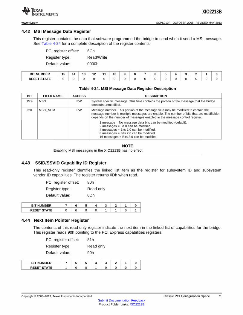
XIO2213B
www.ti.com SCPS210F –OCTOBER 2008–REVISED MAY 2013
4.42 MSI Message Data Register
This register contains the data that software programmed the bridge to send when it send a MSI message.See Table 4-24 for a complete description of the register contents.
PCI register offset: 6Ch
Register type: Read/Write
Default value: 0000h
BIT NUMBER 15 14 13 12 11 10 9 8 7 6 5 4 3 2 1 0
RESET STATE 0 0 0 0 0 0 0 0 0 0 0 0 0 0 0 0
Table 4-24. MSI Message Data Register Description
BIT FIELD NAME ACCESS DESCRIPTION
15:4 MSG RW System specific message. This field contains the portion of the message that the bridgeforwards unmodified.
3:0 MSG_NUM RW Message number. This portion of the message field may be modified to contain themessage number is multiple messages are enable. The number of bits that are modifiabledepends on the number of messages enabled in the message control register.
1 message = No message data bits can be modified (default).2 messages = Bit 0 can be modified.4 messages = Bits 1:0 can be modified.8 messages = Bits 2:0 can be modified.16 messages = Bits 3:0 can be modified.
NOTEEnabling MSI messaging in the XIO2213B has no effect.
4.43 SSID/SSVID Capability ID Register
This read-only register identifies the linked list item as the register for subsystem ID and subsystemvendor ID capabilities. The register returns 0Dh when read.
PCI register offset: 80h
Register type: Read only
Default value: 0Dh
BIT NUMBER 7 6 5 4 3 2 1 0
RESET STATE 0 0 0 0 1 1 0 1
4.44 Next Item Pointer Register
The contents of this read-only register indicate the next item in the linked list of capabilities for the bridge.This register reads 90h pointing to the PCI Express capabilities registers.
PCI register offset: 81h
Register type: Read only
Default value: 90h
BIT NUMBER 7 6 5 4 3 2 1 0
RESET STATE 1 0 0 1 0 0 0 0
Copyright © 2008–2013, Texas Instruments Incorporated Classic PCI Configuration Space 71Submit Documentation FeedbackProduct Folder Links: XIO2213B
XIO2213B
SCPS210F –OCTOBER 2008–REVISED MAY 2013 www.ti.com
4.45 Subsystem Vendor ID Register
This register, used for system and option card identification purposes, may be required for certainoperating systems. This read-only register is initialized through the EEPROM and can be written throughthe subsystem alias register. This register shall only be reset by a fundamental reset (FRST).
PCI register offset: 84h
Register type: Read only
Default value: 0000h
BIT NUMBER 15 14 13 12 11 10 9 8 7 6 5 4 3 2 1 0
RESET STATE 0 0 0 0 0 0 0 0 0 0 0 0 0 0 0 0
4.46 Subsystem ID Register
This register, used for system and option card identification purposes, may be required for certainoperating systems. This read-only register is initialized through the EEPROM and can be written throughthe subsystem alias register. This register shall only be reset by FRST.
PCI register offset: 86h
Register type: Read only
Default value: 0000h
BIT NUMBER 15 14 13 12 11 10 9 8 7 6 5 4 3 2 1 0
RESET STATE 0 0 0 0 0 0 0 0 0 0 0 0 0 0 0 0
4.47 PCI Express Capability ID Register
This read-only register identifies the linked list item as the register for PCIe capabilities. The registerreturns 10h when read.
PCI register offset: 90h
Register type: Read only
Default value: 10h
BIT NUMBER 7 6 5 4 3 2 1 0
RESET STATE 0 0 0 1 0 0 0 0
4.48 Next Item Pointer Register
The contents of this read-only register indicate the next item in the linked list of capabilities for the bridge.This register reads 00h indicating no additional capabilities are supported.
PCI register offset: 91h
Register type: Read only
Default value: 00h
BIT NUMBER 7 6 5 4 3 2 1 0
RESET STATE 0 0 0 0 0 0 0 0
72 Classic PCI Configuration Space Copyright © 2008–2013, Texas Instruments Incorporated
Submit Documentation FeedbackProduct Folder Links: XIO2213B
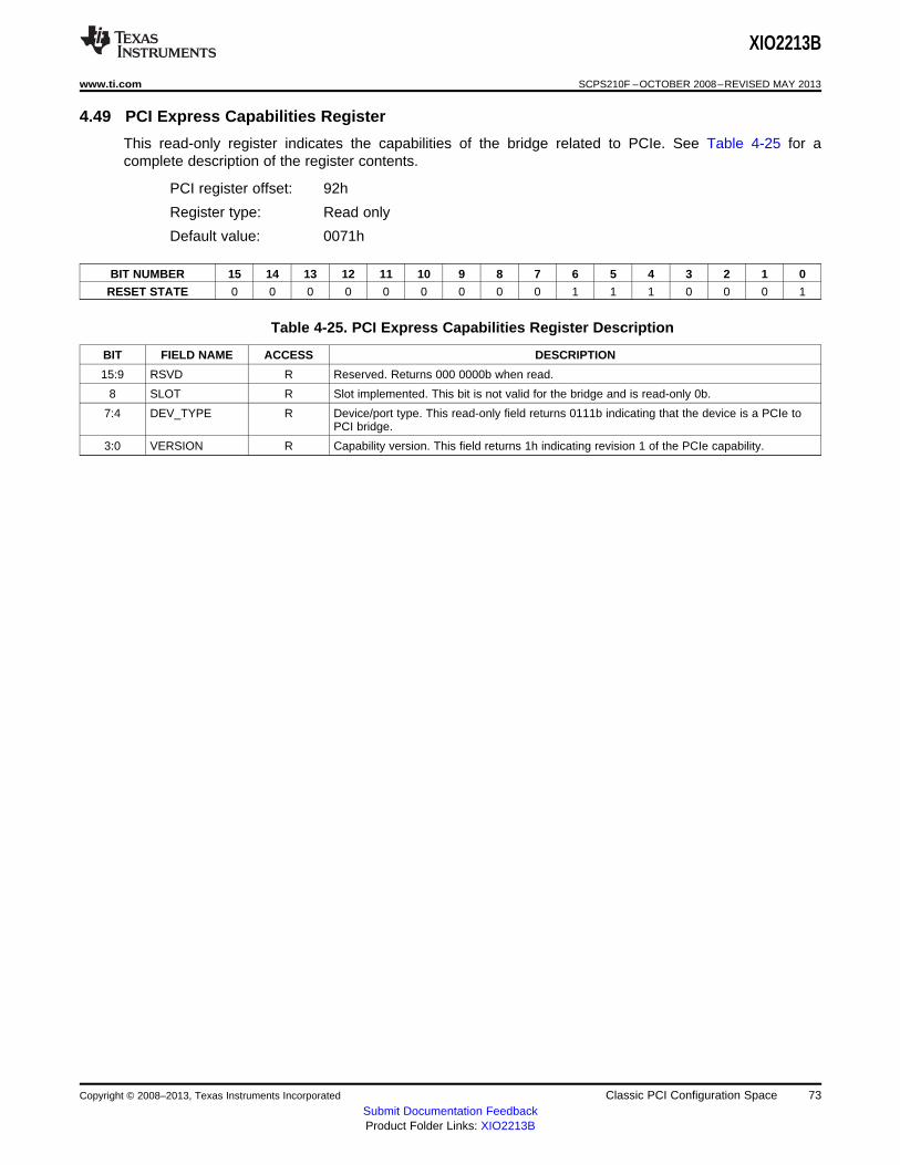
XIO2213B
www.ti.com SCPS210F –OCTOBER 2008–REVISED MAY 2013
4.49 PCI Express Capabilities Register
This read-only register indicates the capabilities of the bridge related to PCIe. See Table 4-25 for acomplete description of the register contents.
PCI register offset: 92h
Register type: Read only
Default value: 0071h
BIT NUMBER 15 14 13 12 11 10 9 8 7 6 5 4 3 2 1 0
RESET STATE 0 0 0 0 0 0 0 0 0 1 1 1 0 0 0 1
Table 4-25. PCI Express Capabilities Register Description
BIT FIELD NAME ACCESS DESCRIPTION
15:9 RSVD R Reserved. Returns 000 0000b when read.
8 SLOT R Slot implemented. This bit is not valid for the bridge and is read-only 0b.
7:4 DEV_TYPE R Device/port type. This read-only field returns 0111b indicating that the device is a PCIe toPCI bridge.
3:0 VERSION R Capability version. This field returns 1h indicating revision 1 of the PCIe capability.
Copyright © 2008–2013, Texas Instruments Incorporated Classic PCI Configuration Space 73Submit Documentation FeedbackProduct Folder Links: XIO2213B
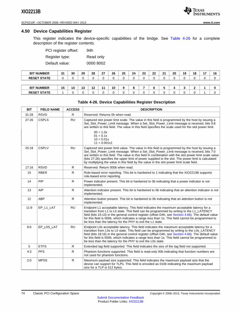
XIO2213B
SCPS210F –OCTOBER 2008–REVISED MAY 2013 www.ti.com
4.50 Device Capabilities Register
This register indicates the device-specific capabilities of the bridge. See Table 4-26 for a completedescription of the register contents.
PCI register offset: 94h
Register type: Read only
Default value: 0000 8002
BIT NUMBER 31 30 29 28 27 26 25 24 23 22 21 20 19 18 17 16
RESET STATE 0 0 0 0 0 0 0 0 0 0 0 0 0 0 0 0
BIT NUMBER 15 14 13 12 11 10 9 8 7 6 5 4 3 2 1 0
RESET STATE 1 0 0 0 0 0 0 0 0 0 0 0 0 0 1 0
Table 4-26. Device Capabilities Register Description
BIT FIELD NAME ACCESS DESCRIPTION
31:28 RSVD R Reserved. Returns 0h when read.
27:26 CSPLS RU Captured slot power limit scale. The value in this field is programmed by the host by issuing aSet_Slot_Power_Limit message. When a Set_Slot_Power_Limit message is received, bits 9:8are written to this field. The value in this field specifies the scale used for the slot power limit.
00 = 1.0x01 = 0.1x10 = 0.01x11 = 0.001x1
25:18 CSPLV RU Captured slot power limit value. The value in this field is programmed by the host by issuing aSet_Slot_Power_Limit message. When a Set_Slot_Power_Limit message is received, bits 7:0are written to this field. The value in this field in combination with the slot power limit scale value(bits 27:26) specifies the upper limit of power supplied to the slot. The power limit is calculatedby multiplying the value in this field by the value in the slot power limit scale field.
17:16 RSVD R Reserved. Return 000b when read.
15 RBER R Role-based error reporting. This bit is hardwired to 1 indicating that the XIO2213B supportsrole-based error reporting.
14 PIP R Power indicator present. This bit is hardwired to 0b indicating that a power indicator is notimplemented.
13 AIP R Attention indicator present. This bit is hardwired to 0b indicating that an attention indicator is notimplemented.
12 ABP R Attention button present. This bit is hardwired to 0b indicating that an attention button is notimplemented.
11:9 EP_L1_LAT RU Endpoint L1 acceptable latency. This field indicates the maximum acceptable latency for atransition from L1 to L0 state. This field can be programmed by writing to the L1_LATENCYfield (bits 15:13) in the general control register (offset D4h, see Section 4.66). The default valuefor this field is 000b, which indicates a range less than 1s. This field cannot be programmed tobe less than the latency for the PHY to exit the L1 state.
8:6 EP_L0S_LAT RU Endpoint L0s acceptable latency. This field indicates the maximum acceptable latency for atransition from L0s to L0 state. This field can be programmed by writing to the L0s_LATENCYfield (bits 18:16) in the general control register (offset D4h, see Section 4.66). The default valuefor this field is 000b, which indicates a range less than 1s. This field cannot be programmed tobe less than the latency for the PHY to exit the L0s state.
5 ETFS R Extended tag field supported. This field indicates the size of the tag field not supported.
4:3 PFS R Phantom functions supported. This field is read-only 00b indicating that function numbers arenot used for phantom functions.
2:0 MPSS R Maximum payload size supported. This field indicates the maximum payload size that thedevice can support for TLPs. This field is encoded as 010b indicating the maximum payloadsize for a TLP is 512 bytes.
74 Classic PCI Configuration Space Copyright © 2008–2013, Texas Instruments Incorporated
Submit Documentation FeedbackProduct Folder Links: XIO2213B
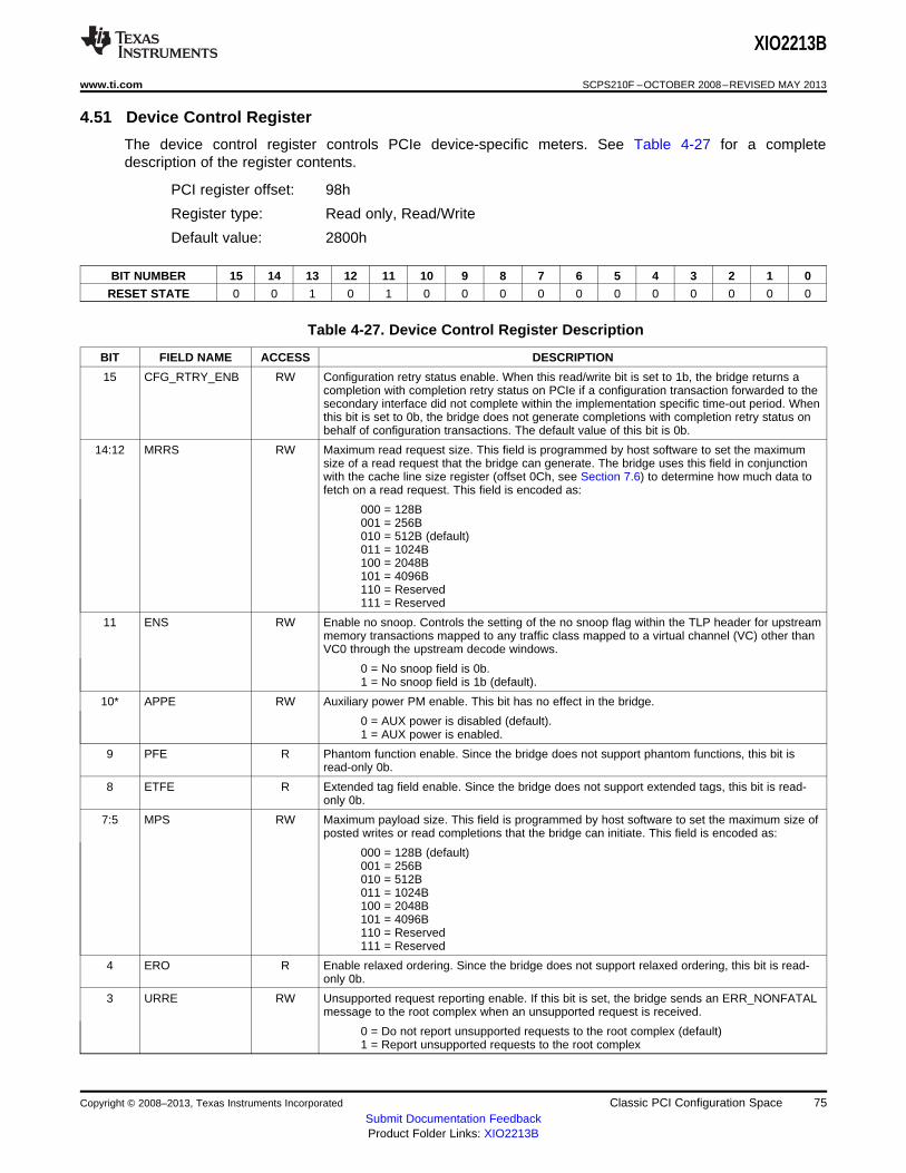
XIO2213B
www.ti.com SCPS210F –OCTOBER 2008–REVISED MAY 2013
4.51 Device Control Register
The device control register controls PCIe device-specific meters. See Table 4-27 for a completedescription of the register contents.
PCI register offset: 98h
Register type: Read only, Read/Write
Default value: 2800h
BIT NUMBER 15 14 13 12 11 10 9 8 7 6 5 4 3 2 1 0
RESET STATE 0 0 1 0 1 0 0 0 0 0 0 0 0 0 0 0
Table 4-27. Device Control Register Description
BIT FIELD NAME ACCESS DESCRIPTION
15 CFG_RTRY_ENB RW Configuration retry status enable. When this read/write bit is set to 1b, the bridge returns acompletion with completion retry status on PCIe if a configuration transaction forwarded to thesecondary interface did not complete within the implementation specific time-out period. Whenthis bit is set to 0b, the bridge does not generate completions with completion retry status onbehalf of configuration transactions. The default value of this bit is 0b.
14:12 MRRS RW Maximum read request size. This field is programmed by host software to set the maximumsize of a read request that the bridge can generate. The bridge uses this field in conjunctionwith the cache line size register (offset 0Ch, see Section 7.6) to determine how much data tofetch on a read request. This field is encoded as:
000 = 128B001 = 256B010 = 512B (default)011 = 1024B100 = 2048B101 = 4096B110 = Reserved111 = Reserved
11 ENS RW Enable no snoop. Controls the setting of the no snoop flag within the TLP header for upstreammemory transactions mapped to any traffic class mapped to a virtual channel (VC) other thanVC0 through the upstream decode windows.
0 = No snoop field is 0b.1 = No snoop field is 1b (default).
10* APPE RW Auxiliary power PM enable. This bit has no effect in the bridge.
0 = AUX power is disabled (default).1 = AUX power is enabled.
9 PFE R Phantom function enable. Since the bridge does not support phantom functions, this bit isread-only 0b.
8 ETFE R Extended tag field enable. Since the bridge does not support extended tags, this bit is read-only 0b.
7:5 MPS RW Maximum payload size. This field is programmed by host software to set the maximum size ofposted writes or read completions that the bridge can initiate. This field is encoded as:
000 = 128B (default)001 = 256B010 = 512B011 = 1024B100 = 2048B101 = 4096B110 = Reserved111 = Reserved
4 ERO R Enable relaxed ordering. Since the bridge does not support relaxed ordering, this bit is read-only 0b.
3 URRE RW Unsupported request reporting enable. If this bit is set, the bridge sends an ERR_NONFATALmessage to the root complex when an unsupported request is received.
0 = Do not report unsupported requests to the root complex (default)1 = Report unsupported requests to the root complex
Copyright © 2008–2013, Texas Instruments Incorporated Classic PCI Configuration Space 75Submit Documentation FeedbackProduct Folder Links: XIO2213B
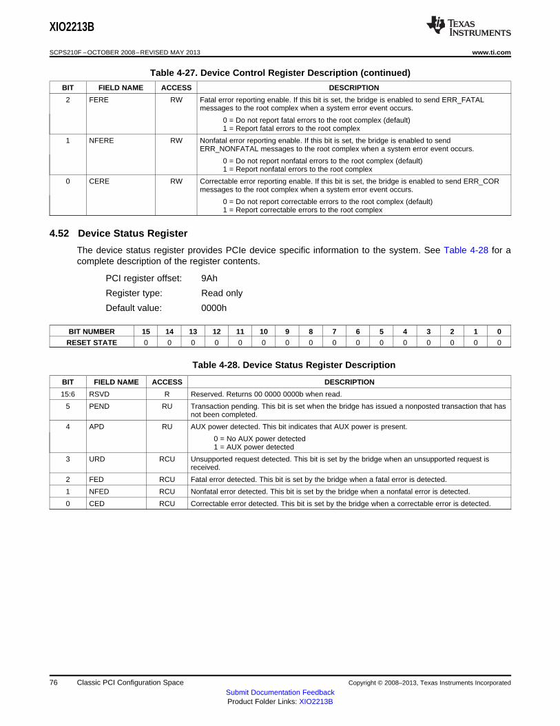
XIO2213B
SCPS210F –OCTOBER 2008–REVISED MAY 2013 www.ti.com
Table 4-27. Device Control Register Description (continued)
BIT FIELD NAME ACCESS DESCRIPTION
2 FERE RW Fatal error reporting enable. If this bit is set, the bridge is enabled to send ERR_FATALmessages to the root complex when a system error event occurs.
0 = Do not report fatal errors to the root complex (default)1 = Report fatal errors to the root complex
1 NFERE RW Nonfatal error reporting enable. If this bit is set, the bridge is enabled to sendERR_NONFATAL messages to the root complex when a system error event occurs.
0 = Do not report nonfatal errors to the root complex (default)1 = Report nonfatal errors to the root complex
0 CERE RW Correctable error reporting enable. If this bit is set, the bridge is enabled to send ERR_CORmessages to the root complex when a system error event occurs.
0 = Do not report correctable errors to the root complex (default)1 = Report correctable errors to the root complex
4.52 Device Status Register
The device status register provides PCIe device specific information to the system. See Table 4-28 for acomplete description of the register contents.
PCI register offset: 9Ah
Register type: Read only
Default value: 0000h
BIT NUMBER 15 14 13 12 11 10 9 8 7 6 5 4 3 2 1 0
RESET STATE 0 0 0 0 0 0 0 0 0 0 0 0 0 0 0 0
Table 4-28. Device Status Register Description
BIT FIELD NAME ACCESS DESCRIPTION
15:6 RSVD R Reserved. Returns 00 0000 0000b when read.
5 PEND RU Transaction pending. This bit is set when the bridge has issued a nonposted transaction that hasnot been completed.
4 APD RU AUX power detected. This bit indicates that AUX power is present.
0 = No AUX power detected1 = AUX power detected
3 URD RCU Unsupported request detected. This bit is set by the bridge when an unsupported request isreceived.
2 FED RCU Fatal error detected. This bit is set by the bridge when a fatal error is detected.
1 NFED RCU Nonfatal error detected. This bit is set by the bridge when a nonfatal error is detected.
0 CED RCU Correctable error detected. This bit is set by the bridge when a correctable error is detected.
76 Classic PCI Configuration Space Copyright © 2008–2013, Texas Instruments Incorporated
Submit Documentation FeedbackProduct Folder Links: XIO2213B
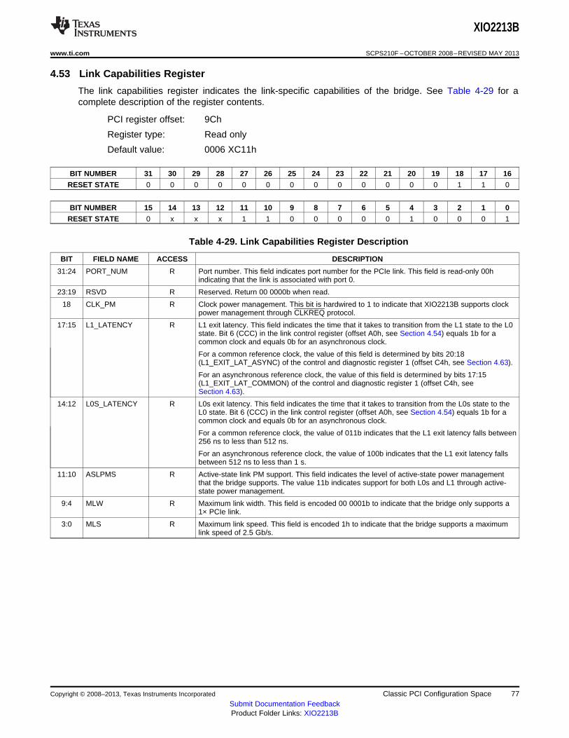
XIO2213B
www.ti.com SCPS210F –OCTOBER 2008–REVISED MAY 2013
4.53 Link Capabilities Register
The link capabilities register indicates the link-specific capabilities of the bridge. See Table 4-29 for acomplete description of the register contents.
PCI register offset: 9Ch
Register type: Read only
Default value: 0006 XC11h
BIT NUMBER 31 30 29 28 27 26 25 24 23 22 21 20 19 18 17 16
RESET STATE 0 0 0 0 0 0 0 0 0 0 0 0 0 1 1 0
BIT NUMBER 15 14 13 12 11 10 9 8 7 6 5 4 3 2 1 0
RESET STATE 0 x x x 1 1 0 0 0 0 0 1 0 0 0 1
Table 4-29. Link Capabilities Register Description
BIT FIELD NAME ACCESS DESCRIPTION
31:24 PORT_NUM R Port number. This field indicates port number for the PCIe link. This field is read-only 00hindicating that the link is associated with port 0.
23:19 RSVD R Reserved. Return 00 0000b when read.
18 CLK_PM R Clock power management. This bit is hardwired to 1 to indicate that XIO2213B supports clockpower management through CLKREQ protocol.
17:15 L1_LATENCY R L1 exit latency. This field indicates the time that it takes to transition from the L1 state to the L0state. Bit 6 (CCC) in the link control register (offset A0h, see Section 4.54) equals 1b for acommon clock and equals 0b for an asynchronous clock.
For a common reference clock, the value of this field is determined by bits 20:18(L1_EXIT_LAT_ASYNC) of the control and diagnostic register 1 (offset C4h, see Section 4.63).
For an asynchronous reference clock, the value of this field is determined by bits 17:15(L1_EXIT_LAT_COMMON) of the control and diagnostic register 1 (offset C4h, seeSection 4.63).
14:12 L0S_LATENCY R L0s exit latency. This field indicates the time that it takes to transition from the L0s state to theL0 state. Bit 6 (CCC) in the link control register (offset A0h, see Section 4.54) equals 1b for acommon clock and equals 0b for an asynchronous clock.
For a common reference clock, the value of 011b indicates that the L1 exit latency falls between256 ns to less than 512 ns.
For an asynchronous reference clock, the value of 100b indicates that the L1 exit latency fallsbetween 512 ns to less than 1 s.
11:10 ASLPMS R Active-state link PM support. This field indicates the level of active-state power managementthat the bridge supports. The value 11b indicates support for both L0s and L1 through active-state power management.
9:4 MLW R Maximum link width. This field is encoded 00 0001b to indicate that the bridge only supports a1× PCIe link.
3:0 MLS R Maximum link speed. This field is encoded 1h to indicate that the bridge supports a maximumlink speed of 2.5 Gb/s.
Copyright © 2008–2013, Texas Instruments Incorporated Classic PCI Configuration Space 77Submit Documentation FeedbackProduct Folder Links: XIO2213B
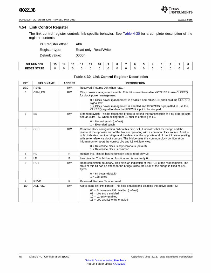
XIO2213B
SCPS210F –OCTOBER 2008–REVISED MAY 2013 www.ti.com
4.54 Link Control Register
The link control register controls link-specific behavior. See Table 4-30 for a complete description of theregister contents.
PCI register offset: A0h
Register type: Read only, Read/Write
Default value: 0000h
BIT NUMBER 15 14 13 12 11 10 9 8 7 6 5 4 3 2 1 0
RESET STATE 0 0 0 0 0 0 0 0 0 0 0 0 0 0 0 0
Table 4-30. Link Control Register Description
BIT FIELD NAME ACCESS DESCRIPTION
15:9 RSVD RW Reserved. Returns 00h when read.
8 CPM_EN RW Clock power management enable. This bit is used to enable XIO2213B to use CLKREQfor clock power management
0 = Clock power management is disabled and XIO2213B shall hold the CLKREQsignal low.1 = Clock power management is enabled and XIO2213B is permitted to use theCLKREQ signal to allow the REFCLK input to be stopped.
7 ES RW Extended synch. This bit forces the bridge to extend the transmission of FTS ordered setsand an extra TS2 when exiting from L1 prior to entering to L0.
0 = Normal synch (default)1 = Extended synch
6 CCC RW Common clock configuration. When this bit is set, it indicates that the bridge and thedevice at the opposite end of the link are operating with a common clock source. A valueof 0b indicates that the bridge and the device at the opposite end of the link are operatingwith se te reference clock sources. The bridge uses this common clock configurationinformation to report the correct L0s and L1 exit latencies.
0 = Reference clock is asynchronous (default).1 = Reference clock is common.
5 RL R Retrain link. This bit has no function and is read-only 0b.
4 LD R Link disable. This bit has no function and is read-only 0b.
3 RCB RW Read completion boundary. This bit is an indication of the RCB of the root complex. Thestate of this bit has no effect on the bridge, since the RCB of the bridge is fixed at 128bytes.
0 = 64 bytes (default)1 = 128 bytes
2 RSVD R Reserved. Returns 0b when read.
1:0 ASLPMC RW Active-state link PM control. This field enables and disables the active-state PM.
00 = Active-state PM disabled (default)01 = L0s entry enabled10 = L1 entry enabled11 = L0s and L1 entry enabled
78 Classic PCI Configuration Space Copyright © 2008–2013, Texas Instruments Incorporated
Submit Documentation FeedbackProduct Folder Links: XIO2213B
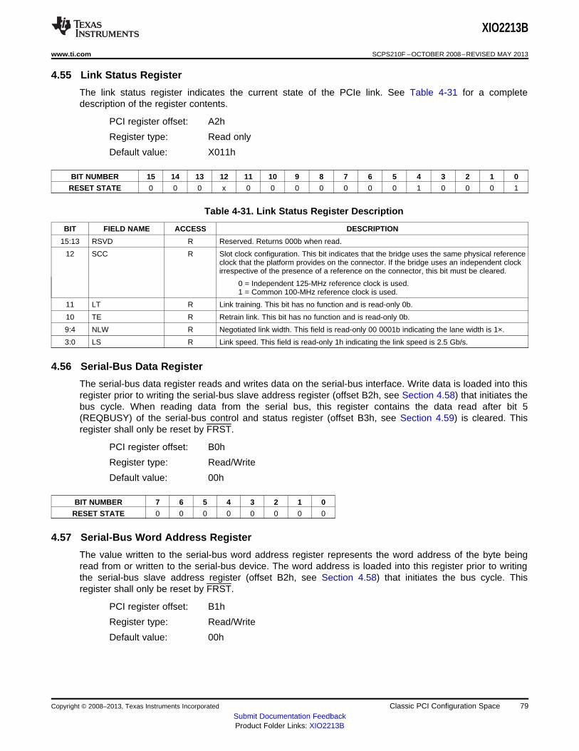
XIO2213B
www.ti.com SCPS210F –OCTOBER 2008–REVISED MAY 2013
4.55 Link Status Register
The link status register indicates the current state of the PCIe link. See Table 4-31 for a completedescription of the register contents.
PCI register offset: A2h
Register type: Read only
Default value: X011h
BIT NUMBER 15 14 13 12 11 10 9 8 7 6 5 4 3 2 1 0
RESET STATE 0 0 0 x 0 0 0 0 0 0 0 1 0 0 0 1
Table 4-31. Link Status Register Description
BIT FIELD NAME ACCESS DESCRIPTION
15:13 RSVD R Reserved. Returns 000b when read.
12 SCC R Slot clock configuration. This bit indicates that the bridge uses the same physical referenceclock that the platform provides on the connector. If the bridge uses an independent clockirrespective of the presence of a reference on the connector, this bit must be cleared.
0 = Independent 125-MHz reference clock is used.1 = Common 100-MHz reference clock is used.
11 LT R Link training. This bit has no function and is read-only 0b.
10 TE R Retrain link. This bit has no function and is read-only 0b.
9:4 NLW R Negotiated link width. This field is read-only 00 0001b indicating the lane width is 1×.
3:0 LS R Link speed. This field is read-only 1h indicating the link speed is 2.5 Gb/s.
4.56 Serial-Bus Data Register
The serial-bus data register reads and writes data on the serial-bus interface. Write data is loaded into thisregister prior to writing the serial-bus slave address register (offset B2h, see Section 4.58) that initiates thebus cycle. When reading data from the serial bus, this register contains the data read after bit 5(REQBUSY) of the serial-bus control and status register (offset B3h, see Section 4.59) is cleared. Thisregister shall only be reset by FRST.
PCI register offset: B0h
Register type: Read/Write
Default value: 00h
BIT NUMBER 7 6 5 4 3 2 1 0
RESET STATE 0 0 0 0 0 0 0 0
4.57 Serial-Bus Word Address Register
The value written to the serial-bus word address register represents the word address of the byte beingread from or written to the serial-bus device. The word address is loaded into this register prior to writingthe serial-bus slave address register (offset B2h, see Section 4.58) that initiates the bus cycle. Thisregister shall only be reset by FRST.
PCI register offset: B1h
Register type: Read/Write
Default value: 00h
Copyright © 2008–2013, Texas Instruments Incorporated Classic PCI Configuration Space 79Submit Documentation FeedbackProduct Folder Links: XIO2213B
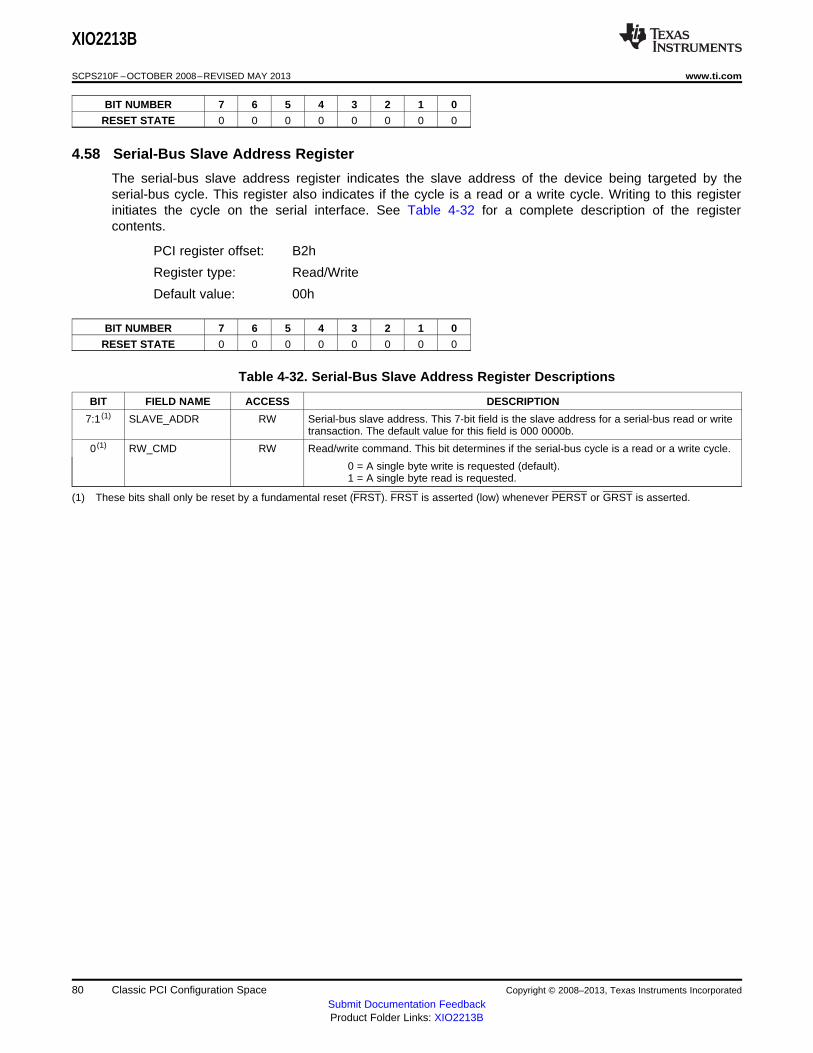
XIO2213B
SCPS210F –OCTOBER 2008–REVISED MAY 2013 www.ti.com
BIT NUMBER 7 6 5 4 3 2 1 0
RESET STATE 0 0 0 0 0 0 0 0
4.58 Serial-Bus Slave Address Register
The serial-bus slave address register indicates the slave address of the device being targeted by theserial-bus cycle. This register also indicates if the cycle is a read or a write cycle. Writing to this registerinitiates the cycle on the serial interface. See Table 4-32 for a complete description of the registercontents.
PCI register offset: B2h
Register type: Read/Write
Default value: 00h
BIT NUMBER 7 6 5 4 3 2 1 0
RESET STATE 0 0 0 0 0 0 0 0
Table 4-32. Serial-Bus Slave Address Register Descriptions
BIT FIELD NAME ACCESS DESCRIPTION
7:1 (1) SLAVE_ADDR RW Serial-bus slave address. This 7-bit field is the slave address for a serial-bus read or writetransaction. The default value for this field is 000 0000b.
0 (1) RW_CMD RW Read/write command. This bit determines if the serial-bus cycle is a read or a write cycle.
0 = A single byte write is requested (default).1 = A single byte read is requested.
(1) These bits shall only be reset by a fundamental reset (FRST). FRST is asserted (low) whenever PERST or GRST is asserted.
80 Classic PCI Configuration Space Copyright © 2008–2013, Texas Instruments Incorporated
Submit Documentation FeedbackProduct Folder Links: XIO2213B
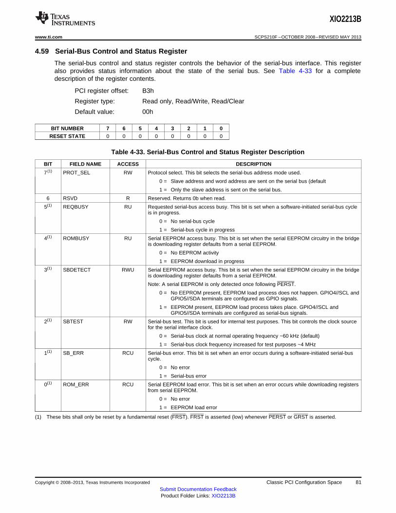
XIO2213B
www.ti.com SCPS210F –OCTOBER 2008–REVISED MAY 2013
4.59 Serial-Bus Control and Status Register
The serial-bus control and status register controls the behavior of the serial-bus interface. This registeralso provides status information about the state of the serial bus. See Table 4-33 for a completedescription of the register contents.
PCI register offset: B3h
Register type: Read only, Read/Write, Read/Clear
Default value: 00h
BIT NUMBER 7 6 5 4 3 2 1 0
RESET STATE 0 0 0 0 0 0 0 0
Table 4-33. Serial-Bus Control and Status Register Description
BIT FIELD NAME ACCESS DESCRIPTION
7 (1) PROT_SEL RW Protocol select. This bit selects the serial-bus address mode used.
0 = Slave address and word address are sent on the serial bus (default
1 = Only the slave address is sent on the serial bus.
6 RSVD R Reserved. Returns 0b when read.
5(1) REQBUSY RU Requested serial-bus access busy. This bit is set when a software-initiated serial-bus cycleis in progress.
0 = No serial-bus cycle
1 = Serial-bus cycle in progress
4(1) ROMBUSY RU Serial EEPROM access busy. This bit is set when the serial EEPROM circuitry in the bridgeis downloading register defaults from a serial EEPROM.
0 = No EEPROM activity
1 = EEPROM download in progress
3(1) SBDETECT RWU Serial EEPROM access busy. This bit is set when the serial EEPROM circuitry in the bridgeis downloading register defaults from a serial EEPROM.
Note: A serial EEPROM is only detected once following PERST.
0 = No EEPROM present, EEPROM load process does not happen. GPIO4//SCL andGPIO5//SDA terminals are configured as GPIO signals.
1 = EEPROM present, EEPROM load process takes place. GPIO4//SCL andGPIO5//SDA terminals are configured as serial-bus signals.
2(1) SBTEST RW Serial-bus test. This bit is used for internal test purposes. This bit controls the clock sourcefor the serial interface clock.
0 = Serial-bus clock at normal operating frequency ~60 kHz (default)
1 = Serial-bus clock frequency increased for test purposes ~4 MHz
1(1) SB_ERR RCU Serial-bus error. This bit is set when an error occurs during a software-initiated serial-buscycle.
0 = No error
1 = Serial-bus error
0(1) ROM_ERR RCU Serial EEPROM load error. This bit is set when an error occurs while downloading registersfrom serial EEPROM.
0 = No error
1 = EEPROM load error
(1) These bits shall only be reset by a fundamental reset (FRST). FRST is asserted (low) whenever PERST or GRST is asserted.
Copyright © 2008–2013, Texas Instruments Incorporated Classic PCI Configuration Space 81Submit Documentation FeedbackProduct Folder Links: XIO2213B
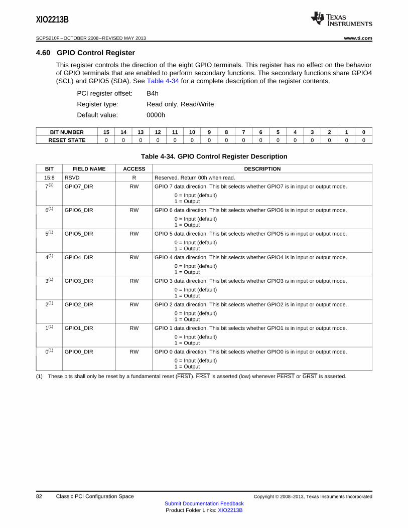
XIO2213B
SCPS210F –OCTOBER 2008–REVISED MAY 2013 www.ti.com
4.60 GPIO Control Register
This register controls the direction of the eight GPIO terminals. This register has no effect on the behaviorof GPIO terminals that are enabled to perform secondary functions. The secondary functions share GPIO4(SCL) and GPIO5 (SDA). See Table 4-34 for a complete description of the register contents.
PCI register offset: B4h
Register type: Read only, Read/Write
Default value: 0000h
BIT NUMBER 15 14 13 12 11 10 9 8 7 6 5 4 3 2 1 0
RESET STATE 0 0 0 0 0 0 0 0 0 0 0 0 0 0 0 0
Table 4-34. GPIO Control Register Description
BIT FIELD NAME ACCESS DESCRIPTION
15:8 RSVD R Reserved. Return 00h when read.
7 (1) GPIO7_DIR RW GPIO 7 data direction. This bit selects whether GPIO7 is in input or output mode.
0 = Input (default)1 = Output
6(1) GPIO6_DIR RW GPIO 6 data direction. This bit selects whether GPIO6 is in input or output mode.
0 = Input (default)1 = Output
5(1) GPIO5_DIR RW GPIO 5 data direction. This bit selects whether GPIO5 is in input or output mode.
0 = Input (default)1 = Output
4(1) GPIO4_DIR RW GPIO 4 data direction. This bit selects whether GPIO4 is in input or output mode.
0 = Input (default)1 = Output
3(1) GPIO3_DIR RW GPIO 3 data direction. This bit selects whether GPIO3 is in input or output mode.
0 = Input (default)1 = Output
2(1) GPIO2_DIR RW GPIO 2 data direction. This bit selects whether GPIO2 is in input or output mode.
0 = Input (default)1 = Output
1(1) GPIO1_DIR RW GPIO 1 data direction. This bit selects whether GPIO1 is in input or output mode.
0 = Input (default)1 = Output
0(1) GPIO0_DIR RW GPIO 0 data direction. This bit selects whether GPIO0 is in input or output mode.
0 = Input (default)1 = Output
(1) These bits shall only be reset by a fundamental reset (FRST). FRST is asserted (low) whenever PERST or GRST is asserted.
82 Classic PCI Configuration Space Copyright © 2008–2013, Texas Instruments Incorporated
Submit Documentation FeedbackProduct Folder Links: XIO2213B
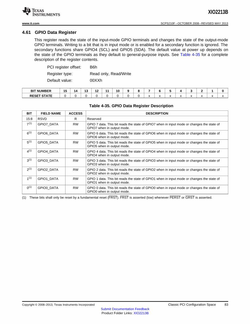
XIO2213B
www.ti.com SCPS210F –OCTOBER 2008–REVISED MAY 2013
4.61 GPIO Data Register
This register reads the state of the input-mode GPIO terminals and changes the state of the output-modeGPIO terminals. Writing to a bit that is in input mode or is enabled for a secondary function is ignored. Thesecondary functions share GPIO4 (SCL) and GPIO5 (SDA). The default value at power up depends onthe state of the GPIO terminals as they default to general-purpose inputs. See Table 4-35 for a completedescription of the register contents.
PCI register offset: B6h
Register type: Read only, Read/Write
Default value: 00XXh
BIT NUMBER 15 14 13 12 11 10 9 8 7 6 5 4 3 2 1 0
RESET STATE 0 0 0 0 0 0 0 0 x x x x x x x x
Table 4-35. GPIO Data Register Description
BIT FIELD NAME ACCESS DESCRIPTION
15:8 RSVD R Reserved
7 (1) GPIO7_DATA RW GPIO 7 data. This bit reads the state of GPIO7 when in input mode or changes the state ofGPIO7 when in output mode.
6(1) GPIO6_DATA RW GPIO 6 data. This bit reads the state of GPIO6 when in input mode or changes the state ofGPIO6 when in output mode.
5(1) GPIO5_DATA RW GPIO 5 data. This bit reads the state of GPIO5 when in input mode or changes the state ofGPIO5 when in output mode.
4(1) GPIO4_DATA RW GPIO 4 data. This bit reads the state of GPIO4 when in input mode or changes the state ofGPIO4 when in output mode.
3(1) GPIO3_DATA RW GPIO 3 data. This bit reads the state of GPIO3 when in input mode or changes the state ofGPIO3 when in output mode.
2(1) GPIO2_DATA RW GPIO 2 data. This bit reads the state of GPIO2 when in input mode or changes the state ofGPIO2 when in output mode.
1(1) GPIO1_DATA RW GPIO 1 data. This bit reads the state of GPIO1 when in input mode or changes the state ofGPIO1 when in output mode.
0(1) GPIO0_DATA RW GPIO 0 data. This bit reads the state of GPIO0 when in input mode or changes the state ofGPIO0 when in output mode.
(1) These bits shall only be reset by a fundamental reset (FRST). FRST is asserted (low) whenever PERST or GRST is asserted.
Copyright © 2008–2013, Texas Instruments Incorporated Classic PCI Configuration Space 83Submit Documentation FeedbackProduct Folder Links: XIO2213B
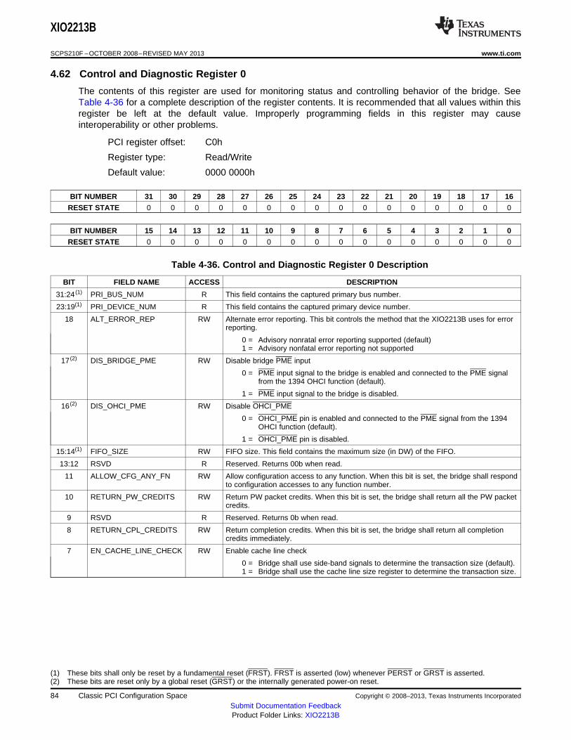
XIO2213B
SCPS210F –OCTOBER 2008–REVISED MAY 2013 www.ti.com
4.62 Control and Diagnostic Register 0
The contents of this register are used for monitoring status and controlling behavior of the bridge. SeeTable 4-36 for a complete description of the register contents. It is recommended that all values within thisregister be left at the default value. Improperly programming fields in this register may causeinteroperability or other problems.
PCI register offset: C0h
Register type: Read/Write
Default value: 0000 0000h
BIT NUMBER 31 30 29 28 27 26 25 24 23 22 21 20 19 18 17 16
RESET STATE 0 0 0 0 0 0 0 0 0 0 0 0 0 0 0 0
BIT NUMBER 15 14 13 12 11 10 9 8 7 6 5 4 3 2 1 0
RESET STATE 0 0 0 0 0 0 0 0 0 0 0 0 0 0 0 0
Table 4-36. Control and Diagnostic Register 0 Description
BIT FIELD NAME ACCESS DESCRIPTION
31:24 (1) PRI_BUS_NUM R This field contains the captured primary bus number.
23:19(1) PRI_DEVICE_NUM R This field contains the captured primary device number.
18 ALT_ERROR_REP RW Alternate error reporting. This bit controls the method that the XIO2213B uses for errorreporting.
0 = Advisory nonratal error reporting supported (default)1 = Advisory nonfatal error reporting not supported
17 (2) DIS_BRIDGE_PME RW Disable bridge PME input
0 = PME input signal to the bridge is enabled and connected to the PME signalfrom the 1394 OHCI function (default).
1 = PME input signal to the bridge is disabled.
16 (2) DIS_OHCI_PME RW Disable OHCI_PME
0 = OHCI_PME pin is enabled and connected to the PME signal from the 1394OHCI function (default).
1 = OHCI_PME pin is disabled.
15:14(1) FIFO_SIZE RW FIFO size. This field contains the maximum size (in DW) of the FIFO.
13:12 RSVD R Reserved. Returns 00b when read.
11 ALLOW_CFG_ANY_FN RW Allow configuration access to any function. When this bit is set, the bridge shall respondto configuration accesses to any function number.
10 RETURN_PW_CREDITS RW Return PW packet credits. When this bit is set, the bridge shall return all the PW packetcredits.
9 RSVD R Reserved. Returns 0b when read.
8 RETURN_CPL_CREDITS RW Return completion credits. When this bit is set, the bridge shall return all completioncredits immediately.
7 EN_CACHE_LINE_CHECK RW Enable cache line check
0 = Bridge shall use side-band signals to determine the transaction size (default).1 = Bridge shall use the cache line size register to determine the transaction size.
(1) These bits shall only be reset by a fundamental reset (FRST). FRST is asserted (low) whenever PERST or GRST is asserted.(2) These bits are reset only by a global reset (GRST) or the internally generated power-on reset.
84 Classic PCI Configuration Space Copyright © 2008–2013, Texas Instruments Incorporated
Submit Documentation FeedbackProduct Folder Links: XIO2213B
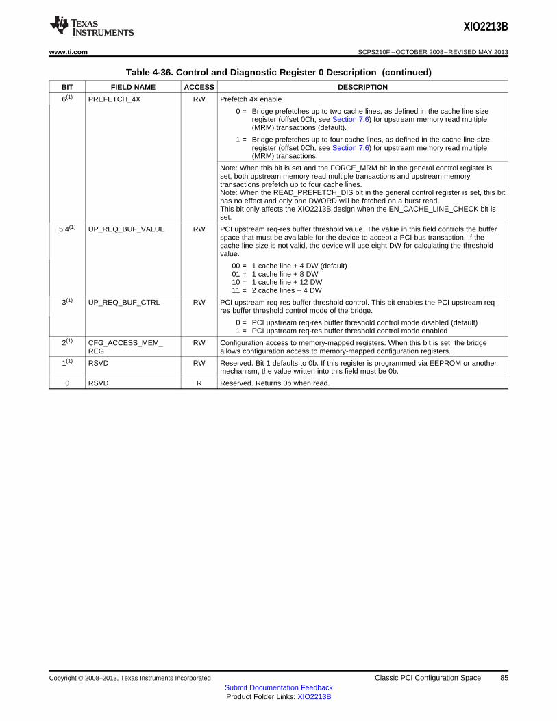
XIO2213B
www.ti.com SCPS210F –OCTOBER 2008–REVISED MAY 2013
Table 4-36. Control and Diagnostic Register 0 Description (continued)
BIT FIELD NAME ACCESS DESCRIPTION
6(1) PREFETCH_4X RW Prefetch 4× enable
0 = Bridge prefetches up to two cache lines, as defined in the cache line sizeregister (offset 0Ch, see Section 7.6) for upstream memory read multiple(MRM) transactions (default).
1 = Bridge prefetches up to four cache lines, as defined in the cache line sizeregister (offset 0Ch, see Section 7.6) for upstream memory read multiple(MRM) transactions.
Note: When this bit is set and the FORCE_MRM bit in the general control register isset, both upstream memory read multiple transactions and upstream memorytransactions prefetch up to four cache lines.Note: When the READ_PREFETCH_DIS bit in the general control register is set, this bithas no effect and only one DWORD will be fetched on a burst read.This bit only affects the XIO2213B design when the EN_CACHE_LINE_CHECK bit isset.
5:4(1) UP_REQ_BUF_VALUE RW PCI upstream req-res buffer threshold value. The value in this field controls the bufferspace that must be available for the device to accept a PCI bus transaction. If thecache line size is not valid, the device will use eight DW for calculating the thresholdvalue.
00 = 1 cache line + 4 DW (default)01 = 1 cache line + 8 DW10 = 1 cache line + 12 DW11 = 2 cache lines + 4 DW
3(1) UP_REQ_BUF_CTRL RW PCI upstream req-res buffer threshold control. This bit enables the PCI upstream req-res buffer threshold control mode of the bridge.
0 = PCI upstream req-res buffer threshold control mode disabled (default)1 = PCI upstream req-res buffer threshold control mode enabled
2(1) CFG_ACCESS_MEM_ RW Configuration access to memory-mapped registers. When this bit is set, the bridgeREG allows configuration access to memory-mapped configuration registers.
1(1) RSVD RW Reserved. Bit 1 defaults to 0b. If this register is programmed via EEPROM or anothermechanism, the value written into this field must be 0b.
0 RSVD R Reserved. Returns 0b when read.
Copyright © 2008–2013, Texas Instruments Incorporated Classic PCI Configuration Space 85Submit Documentation FeedbackProduct Folder Links: XIO2213B
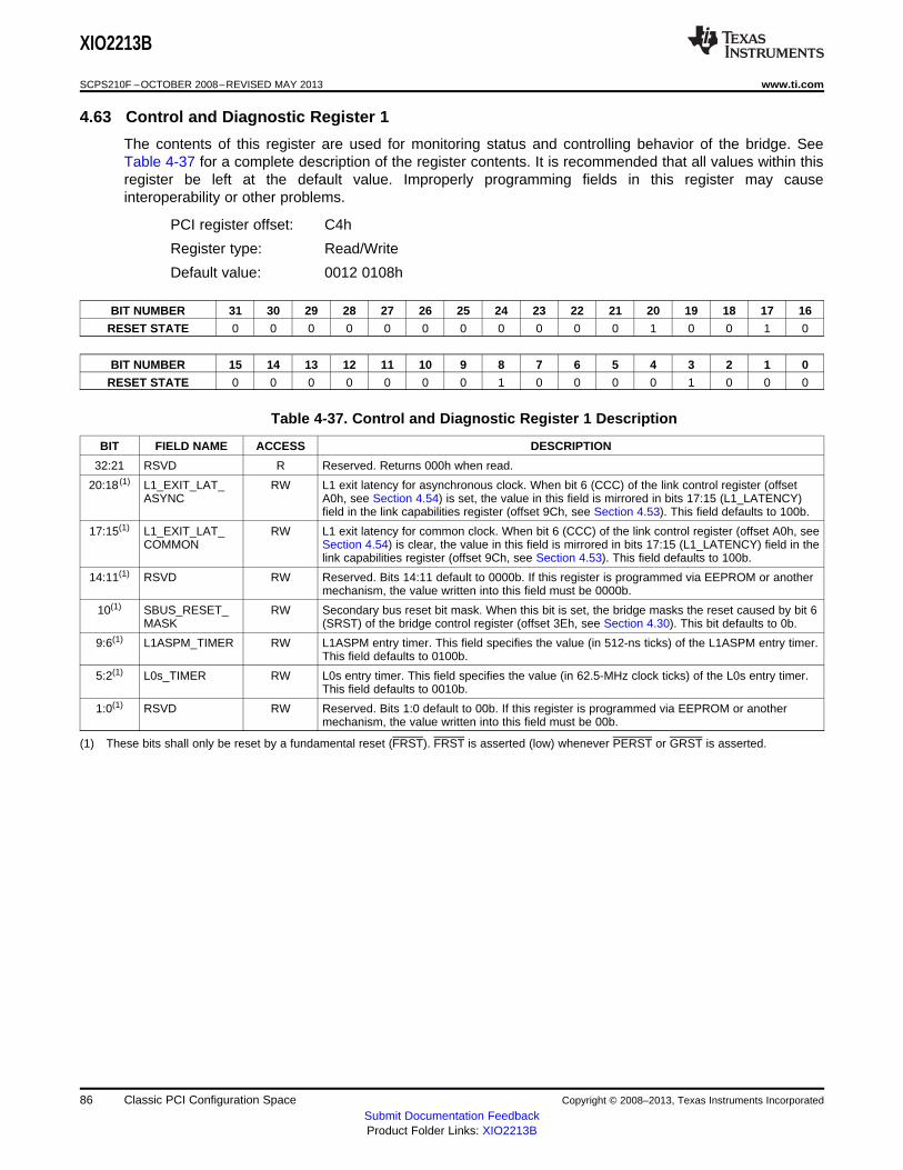
XIO2213B
SCPS210F –OCTOBER 2008–REVISED MAY 2013 www.ti.com
4.63 Control and Diagnostic Register 1
The contents of this register are used for monitoring status and controlling behavior of the bridge. SeeTable 4-37 for a complete description of the register contents. It is recommended that all values within thisregister be left at the default value. Improperly programming fields in this register may causeinteroperability or other problems.
PCI register offset: C4h
Register type: Read/Write
Default value: 0012 0108h
BIT NUMBER 31 30 29 28 27 26 25 24 23 22 21 20 19 18 17 16
RESET STATE 0 0 0 0 0 0 0 0 0 0 0 1 0 0 1 0
BIT NUMBER 15 14 13 12 11 10 9 8 7 6 5 4 3 2 1 0
RESET STATE 0 0 0 0 0 0 0 1 0 0 0 0 1 0 0 0
Table 4-37. Control and Diagnostic Register 1 Description
BIT FIELD NAME ACCESS DESCRIPTION
32:21 RSVD R Reserved. Returns 000h when read.
20:18 (1) L1_EXIT_LAT_ RW L1 exit latency for asynchronous clock. When bit 6 (CCC) of the link control register (offsetASYNC A0h, see Section 4.54) is set, the value in this field is mirrored in bits 17:15 (L1_LATENCY)
field in the link capabilities register (offset 9Ch, see Section 4.53). This field defaults to 100b.
17:15(1) L1_EXIT_LAT_ RW L1 exit latency for common clock. When bit 6 (CCC) of the link control register (offset A0h, seeCOMMON Section 4.54) is clear, the value in this field is mirrored in bits 17:15 (L1_LATENCY) field in the
link capabilities register (offset 9Ch, see Section 4.53). This field defaults to 100b.
14:11(1) RSVD RW Reserved. Bits 14:11 default to 0000b. If this register is programmed via EEPROM or anothermechanism, the value written into this field must be 0000b.
10(1) SBUS_RESET_ RW Secondary bus reset bit mask. When this bit is set, the bridge masks the reset caused by bit 6MASK (SRST) of the bridge control register (offset 3Eh, see Section 4.30). This bit defaults to 0b.
9:6(1) L1ASPM_TIMER RW L1ASPM entry timer. This field specifies the value (in 512-ns ticks) of the L1ASPM entry timer.This field defaults to 0100b.
5:2(1) L0s_TIMER RW L0s entry timer. This field specifies the value (in 62.5-MHz clock ticks) of the L0s entry timer.This field defaults to 0010b.
1:0(1) RSVD RW Reserved. Bits 1:0 default to 00b. If this register is programmed via EEPROM or anothermechanism, the value written into this field must be 00b.
(1) These bits shall only be reset by a fundamental reset (FRST). FRST is asserted (low) whenever PERST or GRST is asserted.
86 Classic PCI Configuration Space Copyright © 2008–2013, Texas Instruments Incorporated
Submit Documentation FeedbackProduct Folder Links: XIO2213B
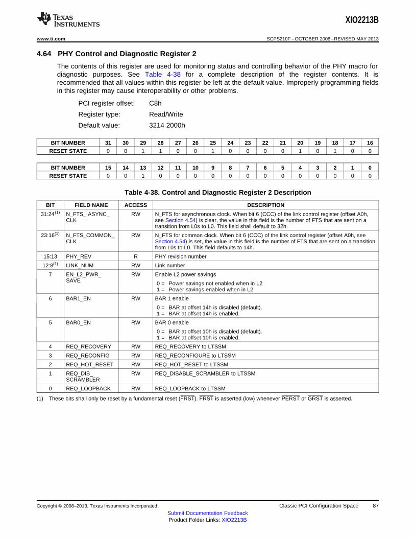
XIO2213B
www.ti.com SCPS210F –OCTOBER 2008–REVISED MAY 2013
4.64 PHY Control and Diagnostic Register 2
The contents of this register are used for monitoring status and controlling behavior of the PHY macro fordiagnostic purposes. See Table 4-38 for a complete description of the register contents. It isrecommended that all values within this register be left at the default value. Improperly programming fieldsin this register may cause interoperability or other problems.
PCI register offset: C8h
Register type: Read/Write
Default value: 3214 2000h
BIT NUMBER 31 30 29 28 27 26 25 24 23 22 21 20 19 18 17 16
RESET STATE 0 0 1 1 0 0 1 0 0 0 0 1 0 1 0 0
BIT NUMBER 15 14 13 12 11 10 9 8 7 6 5 4 3 2 1 0
RESET STATE 0 0 1 0 0 0 0 0 0 0 0 0 0 0 0 0
Table 4-38. Control and Diagnostic Register 2 Description
BIT FIELD NAME ACCESS DESCRIPTION
31:24 (1) N_FTS_ ASYNC_ RW N_FTS for asynchronous clock. When bit 6 (CCC) of the link control register (offset A0h,CLK see Section 4.54) is clear, the value in this field is the number of FTS that are sent on a
transition from L0s to L0. This field shall default to 32h.
23:16(1) N_FTS_COMMON_ RW N_FTS for common clock. When bit 6 (CCC) of the link control register (offset A0h, seeCLK Section 4.54) is set, the value in this field is the number of FTS that are sent on a transition
from L0s to L0. This field defaults to 14h.
15:13 PHY_REV R PHY revision number
12:8(1) LINK_NUM RW Link number
7 EN_L2_PWR_ RW Enable L2 power savingsSAVE 0 = Power savings not enabled when in L2
1 = Power savings enabled when in L2
6 BAR1_EN RW BAR 1 enable
0 = BAR at offset 14h is disabled (default).1 = BAR at offset 14h is enabled.
5 BAR0_EN RW BAR 0 enable
0 = BAR at offset 10h is disabled (default).1 = BAR at offset 10h is enabled.
4 REQ_RECOVERY RW REQ_RECOVERY to LTSSM
3 REQ_RECONFIG RW REQ_RECONFIGURE to LTSSM
2 REQ_HOT_RESET RW REQ_HOT_RESET to LTSSM
1 REQ_DIS_ RW REQ_DISABLE_SCRAMBLER to LTSSMSCRAMBLER
0 REQ_LOOPBACK RW REQ_LOOPBACK to LTSSM
(1) These bits shall only be reset by a fundamental reset (FRST). FRST is asserted (low) whenever PERST or GRST is asserted.
Copyright © 2008–2013, Texas Instruments Incorporated Classic PCI Configuration Space 87Submit Documentation FeedbackProduct Folder Links: XIO2213B
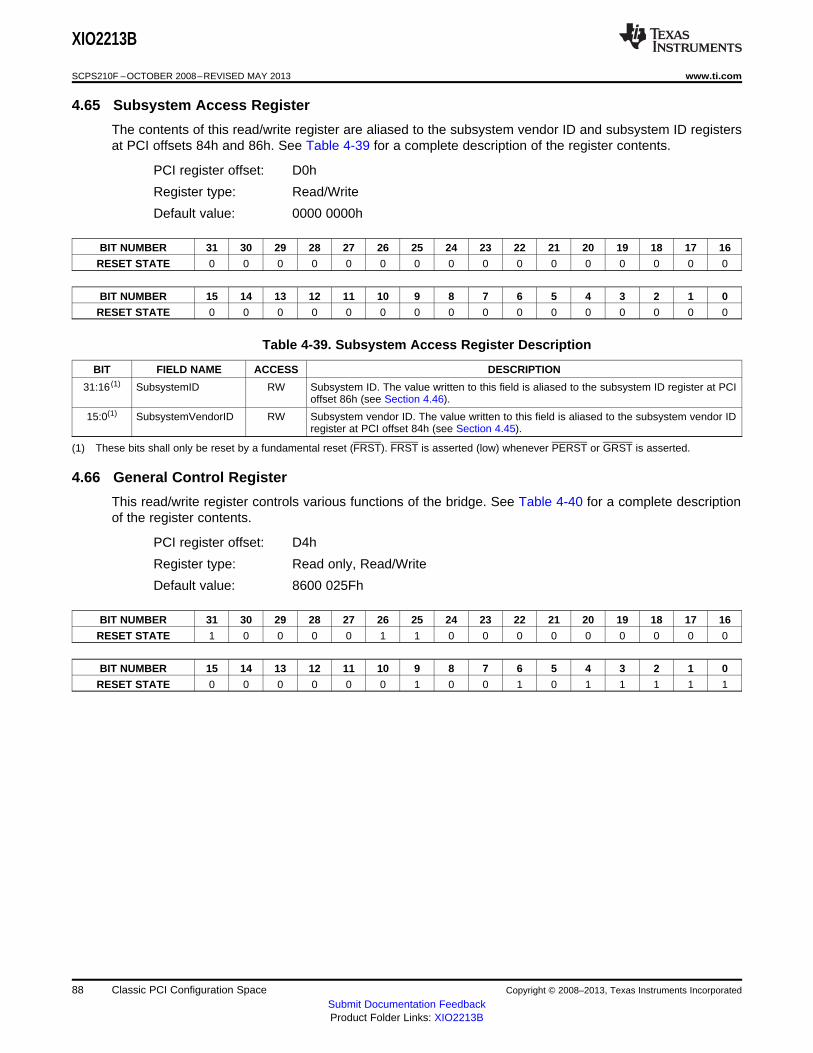
XIO2213B
SCPS210F –OCTOBER 2008–REVISED MAY 2013 www.ti.com
4.65 Subsystem Access Register
The contents of this read/write register are aliased to the subsystem vendor ID and subsystem ID registersat PCI offsets 84h and 86h. See Table 4-39 for a complete description of the register contents.
PCI register offset: D0h
Register type: Read/Write
Default value: 0000 0000h
BIT NUMBER 31 30 29 28 27 26 25 24 23 22 21 20 19 18 17 16
RESET STATE 0 0 0 0 0 0 0 0 0 0 0 0 0 0 0 0
BIT NUMBER 15 14 13 12 11 10 9 8 7 6 5 4 3 2 1 0
RESET STATE 0 0 0 0 0 0 0 0 0 0 0 0 0 0 0 0
Table 4-39. Subsystem Access Register Description
BIT FIELD NAME ACCESS DESCRIPTION
31:16 (1) SubsystemID RW Subsystem ID. The value written to this field is aliased to the subsystem ID register at PCIoffset 86h (see Section 4.46).
15:0(1) SubsystemVendorID RW Subsystem vendor ID. The value written to this field is aliased to the subsystem vendor IDregister at PCI offset 84h (see Section 4.45).
(1) These bits shall only be reset by a fundamental reset (FRST). FRST is asserted (low) whenever PERST or GRST is asserted.
4.66 General Control Register
This read/write register controls various functions of the bridge. See Table 4-40 for a complete descriptionof the register contents.
PCI register offset: D4h
Register type: Read only, Read/Write
Default value: 8600 025Fh
BIT NUMBER 31 30 29 28 27 26 25 24 23 22 21 20 19 18 17 16
RESET STATE 1 0 0 0 0 1 1 0 0 0 0 0 0 0 0 0
BIT NUMBER 15 14 13 12 11 10 9 8 7 6 5 4 3 2 1 0
RESET STATE 0 0 0 0 0 0 1 0 0 1 0 1 1 1 1 1
88 Classic PCI Configuration Space Copyright © 2008–2013, Texas Instruments Incorporated
Submit Documentation FeedbackProduct Folder Links: XIO2213B
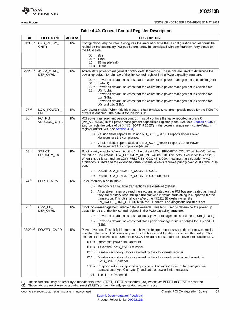
XIO2213B
www.ti.com SCPS210F –OCTOBER 2008–REVISED MAY 2013
Table 4-40. General Control Register Description
BIT FIELD NAME ACCESS DESCRIPTION
31:30 (1) CFG_RETRY_ RW Configuration retry counter. Configures the amount of time that a configuration request must beCNTR retried on the secondary PCI bus before it may be completed with configuration retry status on
the PCIe side.
00 = 25 s01 = 1 ms10 = 25 ms (default)11 = 50 ms
29:28 (1) ASPM_CTRL_ RW Active-state power-management control default override. These bits are used to determine theDEF_OVRD power up default for bits 1:0 of the link control register in the PCIe capability structure.
00 = Power-on default indicates that the active-state power management is disabled (00b)01 = (default).10 = Power-on default indicates that the active-state power management is enabled for11 = L0s (01b).
Power-on default indicates that the active-state power management is enabled forL1s (10b).Power-on default indicates that the active-state power management is enabled forL0s and L1s (11b).
27 (2) LOW_POWER _ RW Low-power enable. When this bit is set, the half-ampitude, no preemphasis mode for the PCIe TXEN drivers is enabled. The default for this bit is 0b.
26 (1) PCI_PM_ RW PCI power management version control. This bit controls the value reported in bits 2:0VERSION_ CTRL (PM_VERSION) in the power management capabilities register (offset 52h, see Section 4.33). It
also controls the value of bit 3 (NO_SOFT_RESET) in the power management control/statusregister (offset 54h, see Section 4.34).
0 = Version fields reports 010b and NO_SOFT_RESET reports 0b for PowerManagement 1.1 compliance.
1 = Version fields reports 011b and NO_SOFT_RESET reports 1b for PowerManagement 1.2 compliance (default).
25 (1) STRICT_ RW Strict priority enable. When this bit is 0, the default LOW_PRIORITY_COUNT will be 001. WhenPRIORITY_EN this bit is 1, the default LOW_PRIORITY_COUNT will be 000. This default value for this bit is 1.
When this bit is set and the LOW_PRIORITY_COUNT is 000, meaning that strict priority VCarbitration is used and the extended virtual channel always receives priority over VC0 at the PCIeport.
0 = Default LOW_PRIORITY_COUNT is 001b.
1 = Default LOW_PRIORITY_COUNT is 000b (default).
24 (1) FORCE_MRM RW Force memory read multiple
0 = Memory read multiple transactions are disabled (default).
1 = All upstream memory read transactions initiated on the PCI bus are treated as thoughthey are memory read multiple transactions in which prefetching is supported for thetransaction. This bit shall only affect the XIO2213B design when theEN_CACHE_LINE_CHECK bit in the TL control and diagnostic register is set.
23 (1) CPM_EN_ RW Clock power-management enable default override. This bit is used to determine the power upDEF_OVRD default for bit 8 of the link control register in the PCIe capability structure.
0 = Power-on default indicates that clock power management is disabled (00b) (default).
1 = Power-on default indicates that clock power management is enabled for L0s and L1(11b).
22:20 (1) POWER_ OVRD RW Power override. This bit field determines how the bridge responds when the slot power limit isless than the amount of power required by the bridge and the devices behind the bridge. Thisfield shall be hardwired to 000b since XIO2213B does not support slot power limit functionality.
000 = Ignore slot power limit (default)
001 = Assert the PWR_OVRD terminal
010 = Disable secondary clocks selected by the clock mask register
011 = Disable secondary clocks selected by the clock mask register and assert thePWR_OVRD terminal
100 = Respond with unsupported request to all transactions except for configurationtransactions (type 0 or type 1) and set slot power limit messages
101, 110, 111 = Reserved
(1) These bits shall only be reset by a fundamental reset (FRST). FRST is asserted (low) whenever PERST or GRST is asserted.(2) These bits are reset only by a global reset (GRST) or the internally generated power-on reset.
Copyright © 2008–2013, Texas Instruments Incorporated Classic PCI Configuration Space 89Submit Documentation FeedbackProduct Folder Links: XIO2213B
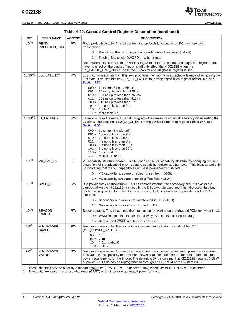
XIO2213B
SCPS210F –OCTOBER 2008–REVISED MAY 2013 www.ti.com
Table 4-40. General Control Register Description (continued)
BIT FIELD NAME ACCESS DESCRIPTION
19 (1) READ_ RW Read prefetch disable. This bit controls the prefetch functionality on PCI memory readPREFETCH_ DIS transactions.
0 = Prefetch to the next cache line boundary on a burst read (default)
1 = Fetch only a single DWORD on a burst read
Note: When this bit is set, the PREFETCH_4X bit in the TL control and diagnostic register shallhave no effect on the design. This bit shall only affect the XIO2213B when theEN_CACHE_LINE_CHECK bit in the TL control and diagnostic register is set.
18:16 (1) L0s_LATENCY RW L0s maximum exit latency. This field programs the maximum acceptable latency when exiting theL0s state. This sets bits 8:6 (EP_L0S_LAT) in the device capabilities register (offset 94h, seeSection 4.50).
000 = Less than 64 ns (default)001 = 64 ns up to less than 128 ns010 = 128 ns up to less than 256 ns011 = 256 ns up to less than 512 ns100 = 512 ns up to less than 1 s101 = 1 s up to less than 2 s110 = 2 s to 4 s111 = More than 4 s
15:13 (3) L1_LATENCY RW L1 maximum exit latency. This field programs the maximum acceptable latency when exiting theL1 state. This sets bits 11:9 (EP_L1_LAT) in the device capabilities register (offset 94h, seeSection 4.50).
000 = Less than 1 s (default)001 = 1 s up to less than 2 s010 = 2 s up to less than 4 s011 = 4 s up to less than 8 s100 = 8 s up to less than 16 s101 = 6 s up to less than 32 s110 = 32 s to 64 s111 = More than 64 s
12 (3) VC_CAP_EN R VC capability structure enable. This bit enables the VC capability structure by changing the nextoffset field of the advanced error reporting capability register at offset 102h. This bit is a read only0b indicating that the VC capability structure is permanently disabled.
0 = VC capability structure disabled (offset field = 000h)
1 = VC capability structure enabled (offset field = 150h)
11 (3) BPCC_E RW Bus power clock control enable. This bit controls whether the secondary bus PCI clocks arestopped when the XIO2213B is placed in the D3 state. It is assumed that if the secondary busclocks are required to be active that a reference clock continues to be provided on the PCIeinterface.
0 = Secondary bus clocks are not stopped in D3 (default).
1 = Secondary bus clocks are stopped on D3.
10 (4) BEACON_ RW Beacon enable. This bit controls the mechanism for waking up the physical PCIe link when in L2.ENABLE 0 = WAKE mechanism is used exclusively. Beacon is not used (default).
1 = Beacon and WAKE mechanisms are used.
9:8 (3) MIN_POWER_ RW Minimum power scale. This value is programmed to indicate the scale of bits 7:0SCALE (MIN_POWER_VALUE).
00 = 1.0x01 = 0.1x10 = 0.01x (default)11 = 0.001x
7:0 (3) MIN_POWER_ RW Minimum power value. This value is programmed to indicate the minimum power requirements.VALUE This value is multiplied by the minimum power scale field (bits 9:8) to determine the minimum
power requirements for the bridge. The default is 5Fh, indicating that XIO2213B requires 0.95 Wof power. This field can be reprogrammed through an EEPROM or the system BIOS.
(3) These bits shall only be reset by a fundamental reset (FRST). FRST is asserted (low) whenever PERST or GRST is asserted.(4) These bits are reset only by a global reset (GRST) or the internally generated power-on reset.
90 Classic PCI Configuration Space Copyright © 2008–2013, Texas Instruments Incorporated
Submit Documentation FeedbackProduct Folder Links: XIO2213B
XIO2213B
www.ti.com SCPS210F –OCTOBER 2008–REVISED MAY 2013
4.67 TI Proprietary Register
This read/write TI proprietary register is located at offset D8h and controls TI proprietary functions. Thisregister must not be changed from the specified default state. This register shall only be reset by FRST.
PCI register offset: D8h
Register type: Read only, Read/Write
Default value: 00h
BIT NUMBER 7 6 5 4 3 2 1 0
RESET STATE 0 0 0 0 0 0 0 0
4.68 TI Proprietary Register
This read/write TI proprietary register is located at offset D9h and controls TI proprietary functions. Thisregister must not be changed from the specified default state. This register shall only be reset by FRST.
PCI register offset: D9h
Register type: Read only, Read/Write
Default value: 00h
BIT NUMBER 7 6 5 4 3 2 1 0
RESET STATE 0 0 0 0 0 0 0 0
4.69 TI Proprietary Register
This read-only TI proprietary register is located at offset DAh and controls TI proprietary functions. Thisregister must not be changed from the specified default state. This register shall only be reset by FRST.
PCI register offset: DAh
Register type: Read only
Default value: 00h
BIT NUMBER 7 6 5 4 3 2 1 0
RESET STATE 0 0 0 0 0 0 0 0
Copyright © 2008–2013, Texas Instruments Incorporated Classic PCI Configuration Space 91Submit Documentation FeedbackProduct Folder Links: XIO2213B
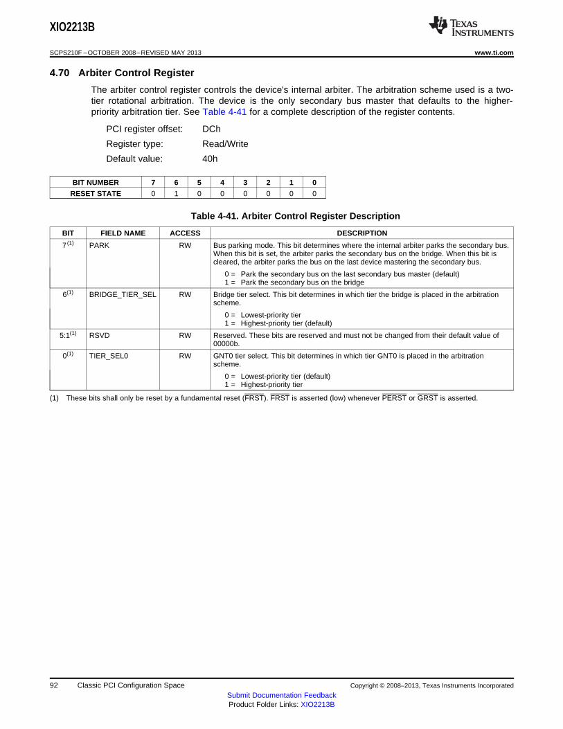
XIO2213B
SCPS210F –OCTOBER 2008–REVISED MAY 2013 www.ti.com
4.70 Arbiter Control Register
The arbiter control register controls the device's internal arbiter. The arbitration scheme used is a two-tier rotational arbitration. The device is the only secondary bus master that defaults to the higher-priority arbitration tier. See Table 4-41 for a complete description of the register contents.
PCI register offset: DCh
Register type: Read/Write
Default value: 40h
BIT NUMBER 7 6 5 4 3 2 1 0
RESET STATE 0 1 0 0 0 0 0 0
Table 4-41. Arbiter Control Register Description
BIT FIELD NAME ACCESS DESCRIPTION
7 (1) PARK RW Bus parking mode. This bit determines where the internal arbiter parks the secondary bus.When this bit is set, the arbiter parks the secondary bus on the bridge. When this bit iscleared, the arbiter parks the bus on the last device mastering the secondary bus.
0 = Park the secondary bus on the last secondary bus master (default)1 = Park the secondary bus on the bridge
6(1) BRIDGE_TIER_SEL RW Bridge tier select. This bit determines in which tier the bridge is placed in the arbitrationscheme.
0 = Lowest-priority tier1 = Highest-priority tier (default)
5:1(1) RSVD RW Reserved. These bits are reserved and must not be changed from their default value of00000b.
0(1) TIER_SEL0 RW GNT0 tier select. This bit determines in which tier GNT0 is placed in the arbitrationscheme.
0 = Lowest-priority tier (default)1 = Highest-priority tier
(1) These bits shall only be reset by a fundamental reset (FRST). FRST is asserted (low) whenever PERST or GRST is asserted.
92 Classic PCI Configuration Space Copyright © 2008–2013, Texas Instruments Incorporated
Submit Documentation FeedbackProduct Folder Links: XIO2213B
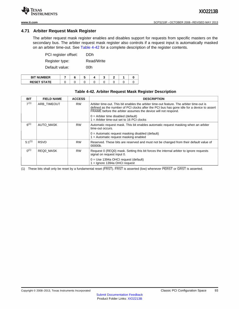
XIO2213B
www.ti.com SCPS210F –OCTOBER 2008–REVISED MAY 2013
4.71 Arbiter Request Mask Register
The arbiter request mask register enables and disables support for requests from specific masters on thesecondary bus. The arbiter request mask register also controls if a request input is automatically maskedon an arbiter time-out. See Table 4-42 for a complete description of the register contents.
PCI register offset: DDh
Register type: Read/Write
Default value: 00h
BIT NUMBER 7 6 5 4 3 2 1 0
RESET STATE 0 0 0 0 0 0 0 0
Table 4-42. Arbiter Request Mask Register Description
BIT FIELD NAME ACCESS DESCRIPTION
7 (1) ARB_TIMEOUT RW Arbiter time-out. This bit enables the arbiter time-out feature. The arbiter time-out isdefined as the number of PCI clocks after the PCI bus has gone idle for a device to assertFRAME before the arbiter assumes the device will not respond.
0 = Arbiter time disabled (default)1 = Arbiter time-out set to 16 PCI clocks
6(1) AUTO_MASK RW Automatic request mask. This bit enables automatic request masking when an arbitertime-out occurs.
0 = Automatic request masking disabled (default)1 = Automatic request masking enabled
5:1(1) RSVD RW Reserved. These bits are reserved and must not be changed from their default value of00000b.
0(1) REQ0_MASK RW Request 0 (REQ0) mask. Setting this bit forces the internal arbiter to ignore requestssignal on request input 0.
0 = Use 1394a OHCI request (default)1 = Ignore 1394a OHCI request
(1) These bits shall only be reset by a fundamental reset (FRST). FRST is asserted (low) whenever PERST or GRST is asserted.
Copyright © 2008–2013, Texas Instruments Incorporated Classic PCI Configuration Space 93Submit Documentation FeedbackProduct Folder Links: XIO2213B
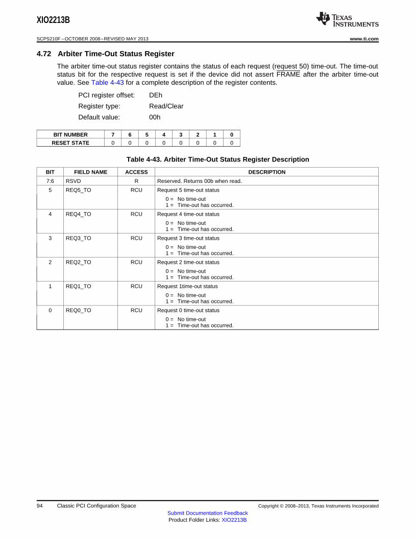
XIO2213B
SCPS210F –OCTOBER 2008–REVISED MAY 2013 www.ti.com
4.72 Arbiter Time-Out Status Register
The arbiter time-out status register contains the status of each request (request 50) time-out. The time-outstatus bit for the respective request is set if the device did not assert FRAME after the arbiter time-outvalue. See Table 4-43 for a complete description of the register contents.
PCI register offset: DEh
Register type: Read/Clear
Default value: 00h
BIT NUMBER 7 6 5 4 3 2 1 0
RESET STATE 0 0 0 0 0 0 0 0
Table 4-43. Arbiter Time-Out Status Register Description
BIT FIELD NAME ACCESS DESCRIPTION
7:6 RSVD R Reserved. Returns 00b when read.
5 REQ5_TO RCU Request 5 time-out status
0 = No time-out1 = Time-out has occurred.
4 REQ4_TO RCU Request 4 time-out status
0 = No time-out1 = Time-out has occurred.
3 REQ3_TO RCU Request 3 time-out status
0 = No time-out1 = Time-out has occurred.
2 REQ2_TO RCU Request 2 time-out status
0 = No time-out1 = Time-out has occurred.
1 REQ1_TO RCU Request 1time-out status
0 = No time-out1 = Time-out has occurred.
0 REQ0_TO RCU Request 0 time-out status
0 = No time-out1 = Time-out has occurred.
94 Classic PCI Configuration Space Copyright © 2008–2013, Texas Instruments Incorporated
Submit Documentation FeedbackProduct Folder Links: XIO2213B
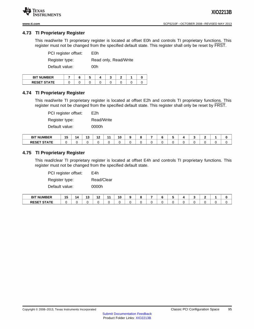
XIO2213B
www.ti.com SCPS210F –OCTOBER 2008–REVISED MAY 2013
4.73 TI Proprietary Register
This read/write TI proprietary register is located at offset E0h and controls TI proprietary functions. Thisregister must not be changed from the specified default state. This register shall only be reset by FRST.
PCI register offset: E0h
Register type: Read only, Read/Write
Default value: 00h
BIT NUMBER 7 6 5 4 3 2 1 0
RESET STATE 0 0 0 0 0 0 0 0
4.74 TI Proprietary Register
This read/write TI proprietary register is located at offset E2h and controls TI proprietary functions. Thisregister must not be changed from the specified default state. This register shall only be reset by FRST.
PCI register offset: E2h
Register type: Read/Write
Default value: 0000h
BIT NUMBER 15 14 13 12 11 10 9 8 7 6 5 4 3 2 1 0
RESET STATE 0 0 0 0 0 0 0 0 0 0 0 0 0 0 0 0
4.75 TI Proprietary Register
This read/clear TI proprietary register is located at offset E4h and controls TI proprietary functions. Thisregister must not be changed from the specified default state.
PCI register offset: E4h
Register type: Read/Clear
Default value: 0000h
BIT NUMBER 15 14 13 12 11 10 9 8 7 6 5 4 3 2 1 0
RESET STATE 0 0 0 0 0 0 0 0 0 0 0 0 0 0 0 0
Copyright © 2008–2013, Texas Instruments Incorporated Classic PCI Configuration Space 95Submit Documentation FeedbackProduct Folder Links: XIO2213B
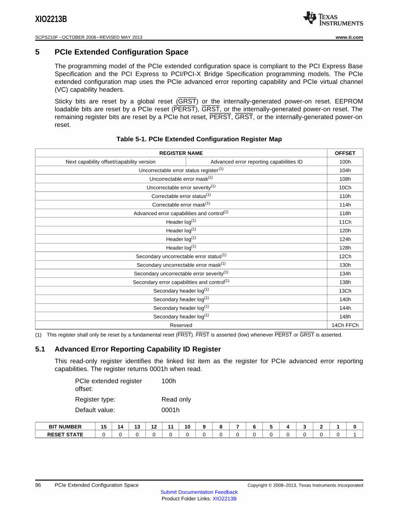
XIO2213B
SCPS210F –OCTOBER 2008–REVISED MAY 2013 www.ti.com
5 PCIe Extended Configuration Space
The programming model of the PCIe extended configuration space is compliant to the PCI Express BaseSpecification and the PCI Express to PCI/PCI-X Bridge Specification programming models. The PCIeextended configuration map uses the PCIe advanced error reporting capability and PCIe virtual channel(VC) capability headers.
Sticky bits are reset by a global reset (GRST) or the internally-generated power-on reset. EEPROMloadable bits are reset by a PCIe reset (PERST), GRST, or the internally-generated power-on reset. Theremaining register bits are reset by a PCIe hot reset, PERST, GRST, or the internally-generated power-onreset.
Table 5-1. PCIe Extended Configuration Register Map
REGISTER NAME OFFSET
Next capability offset/capability version Advanced error reporting capabilities ID 100h
Uncorrectable error status register (1) 104h
Uncorrectable error mask(1) 108h
Uncorrectable error severity(1) 10Ch
Correctable error status(1) 110h
Correctable error mask(1) 114h
Advanced error capabilities and control(1) 118h
Header log(1) 11Ch
Header log(1) 120h
Header log(1) 124h
Header log(1) 128h
Secondary uncorrectable error status(1) 12Ch
Secondary uncorrectable error mask(1) 130h
Secondary uncorrectable error severity(1) 134h
Secondary error capabilities and control(1) 138h
Secondary header log(1) 13Ch
Secondary header log(1) 140h
Secondary header log(1) 144h
Secondary header log(1) 148h
Reserved 14Ch FFCh
(1) This register shall only be reset by a fundamental reset (FRST). FRST is asserted (low) whenever PERST or GRST is asserted.
5.1 Advanced Error Reporting Capability ID Register
This read-only register identifies the linked list item as the register for PCIe advanced error reportingcapabilities. The register returns 0001h when read.
PCIe extended register 100hoffset:
Register type: Read only
Default value: 0001h
BIT NUMBER 15 14 13 12 11 10 9 8 7 6 5 4 3 2 1 0
RESET STATE 0 0 0 0 0 0 0 0 0 0 0 0 0 0 0 1
96 PCIe Extended Configuration Space Copyright © 2008–2013, Texas Instruments Incorporated
Submit Documentation FeedbackProduct Folder Links: XIO2213B
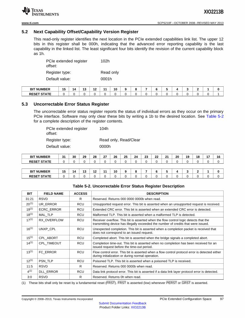
XIO2213B
www.ti.com SCPS210F –OCTOBER 2008–REVISED MAY 2013
5.2 Next Capability Offset/Capability Version Register
This read-only register identifies the next location in the PCIe extended capabilities link list. The upper 12bits in this register shall be 000h, indicating that the advanced error reporting capability is the lastcapability in the linked list. The least significant four bits identify the revision of the current capability blockas 1h.
PCIe extended register 102hoffset:
Register type: Read only
Default value: 0001h
BIT NUMBER 15 14 13 12 11 10 9 8 7 6 5 4 3 2 1 0
RESET STATE 0 0 0 0 0 0 0 0 0 0 0 0 0 0 0 1
5.3 Uncorrectable Error Status Register
The uncorrectable error status register reports the status of individual errors as they occur on the primaryPCIe interface. Software may only clear these bits by writing a 1b to the desired location. See Table 5-2for a complete description of the register contents.
PCIe extended register 104hoffset:
Register type: Read only, Read/Clear
Default value: 0000h
BIT NUMBER 31 30 29 28 27 26 25 24 23 22 21 20 19 18 17 16
RESET STATE 0 0 0 0 0 0 0 0 0 0 0 0 0 0 0 0
BIT NUMBER 15 14 13 12 11 10 9 8 7 6 5 4 3 2 1 0
RESET STATE 0 0 0 0 0 0 0 0 0 0 0 0 0 0 0 0
Table 5-2. Uncorrectable Error Status Register Description
BIT FIELD NAME ACCESS DESCRIPTION
31:21 RSVD R Reserved. Returns 000 0000 0000b when read.
20 (1) UR_ERROR RCU Unsupported request error. This bit is asserted when an unsupported request is received.
19(1) ECRC_ERROR RCU Extended CRC error. This bit is asserted when an extended CRC error is detected.
18(1) MAL_TLP RCU Malformed TLP. This bit is asserted when a malformed TLP is detected.
17(1) RX_OVERFLOW RCU Receiver overflow. This bit is asserted when the flow control logic detects that thetransmitting device has illegally exceeded the number of credits that were issued.
16(1) UNXP_CPL RCU Unexpected completion. This bit is asserted when a completion packet is received thatdoes not correspond to an issued request.
15(1) CPL_ABORT RCU Completed abort. This bit is asserted when the bridge signals a completed abort.
14(1) CPL_TIMEOUT RCU Completion time-out. This bit is asserted when no completion has been received for anissued request before the time-out period.
13(1) FC_ERROR RCU Flow control error. This bit is asserted when a flow control protocol error is detected eitherduring initialization or during normal operation.
12(1) PSN_TLP RCU Poisoned TLP. This bit is asserted when a poisoned TLP is received.
11:5 RSVD R Reserved. Returns 000 0000b when read.
4(1) DLL_ERROR RCU Data link protocol error. This bit is asserted if a data link layer protocol error is detected.
3:0 RSVD R Reserved. Returns 0h when read.
(1) These bits shall only be reset by a fundamental reset (FRST). FRST is asserted (low) whenever PERST or GRST is asserted.
Copyright © 2008–2013, Texas Instruments Incorporated PCIe Extended Configuration Space 97Submit Documentation FeedbackProduct Folder Links: XIO2213B
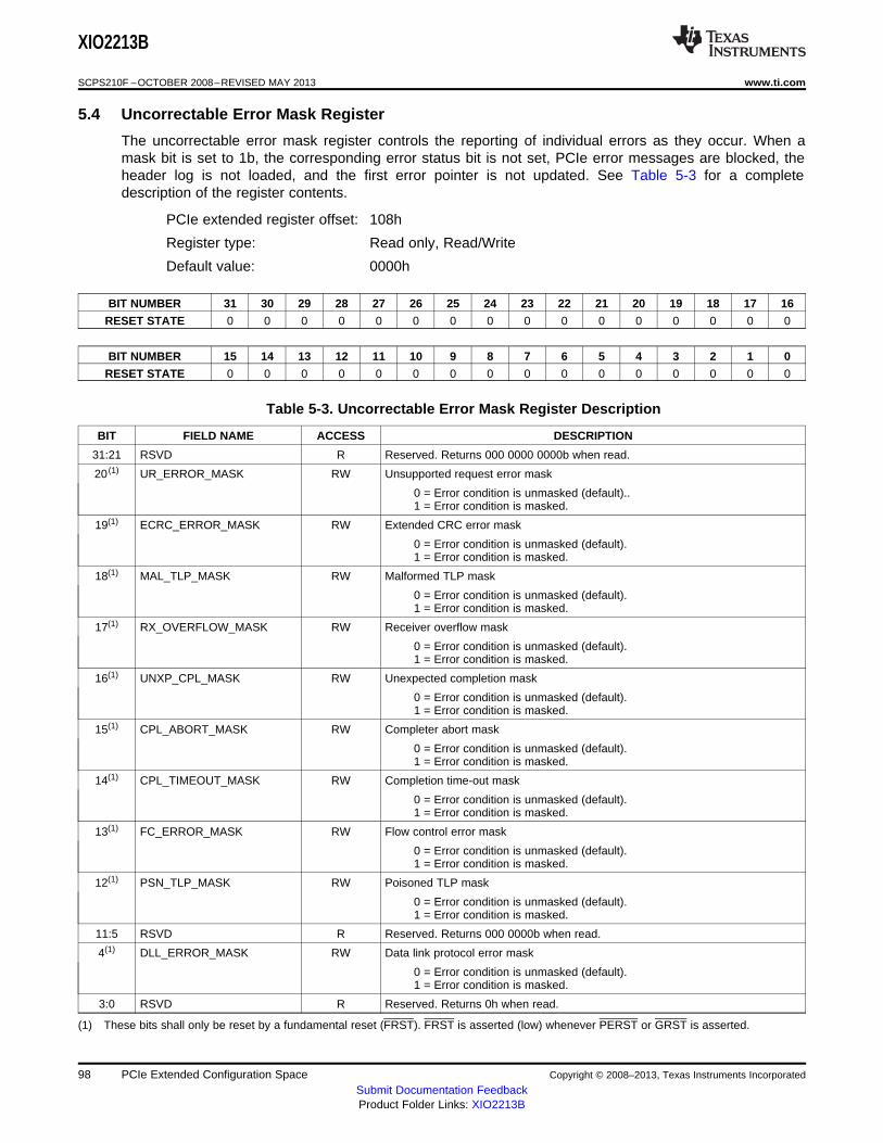
XIO2213B
SCPS210F –OCTOBER 2008–REVISED MAY 2013 www.ti.com
5.4 Uncorrectable Error Mask Register
The uncorrectable error mask register controls the reporting of individual errors as they occur. When amask bit is set to 1b, the corresponding error status bit is not set, PCIe error messages are blocked, theheader log is not loaded, and the first error pointer is not updated. See Table 5-3 for a completedescription of the register contents.
PCIe extended register offset: 108h
Register type: Read only, Read/Write
Default value: 0000h
BIT NUMBER 31 30 29 28 27 26 25 24 23 22 21 20 19 18 17 16
RESET STATE 0 0 0 0 0 0 0 0 0 0 0 0 0 0 0 0
BIT NUMBER 15 14 13 12 11 10 9 8 7 6 5 4 3 2 1 0
RESET STATE 0 0 0 0 0 0 0 0 0 0 0 0 0 0 0 0
Table 5-3. Uncorrectable Error Mask Register Description
BIT FIELD NAME ACCESS DESCRIPTION
31:21 RSVD R Reserved. Returns 000 0000 0000b when read.
20 (1) UR_ERROR_MASK RW Unsupported request error mask
0 = Error condition is unmasked (default)..1 = Error condition is masked.
19(1) ECRC_ERROR_MASK RW Extended CRC error mask
0 = Error condition is unmasked (default).1 = Error condition is masked.
18(1) MAL_TLP_MASK RW Malformed TLP mask
0 = Error condition is unmasked (default).1 = Error condition is masked.
17(1) RX_OVERFLOW_MASK RW Receiver overflow mask
0 = Error condition is unmasked (default).1 = Error condition is masked.
16(1) UNXP_CPL_MASK RW Unexpected completion mask
0 = Error condition is unmasked (default).1 = Error condition is masked.
15(1) CPL_ABORT_MASK RW Completer abort mask
0 = Error condition is unmasked (default).1 = Error condition is masked.
14(1) CPL_TIMEOUT_MASK RW Completion time-out mask
0 = Error condition is unmasked (default).1 = Error condition is masked.
13(1) FC_ERROR_MASK RW Flow control error mask
0 = Error condition is unmasked (default).1 = Error condition is masked.
12(1) PSN_TLP_MASK RW Poisoned TLP mask
0 = Error condition is unmasked (default).1 = Error condition is masked.
11:5 RSVD R Reserved. Returns 000 0000b when read.
4(1) DLL_ERROR_MASK RW Data link protocol error mask
0 = Error condition is unmasked (default).1 = Error condition is masked.
3:0 RSVD R Reserved. Returns 0h when read.
(1) These bits shall only be reset by a fundamental reset (FRST). FRST is asserted (low) whenever PERST or GRST is asserted.
98 PCIe Extended Configuration Space Copyright © 2008–2013, Texas Instruments Incorporated
Submit Documentation FeedbackProduct Folder Links: XIO2213B
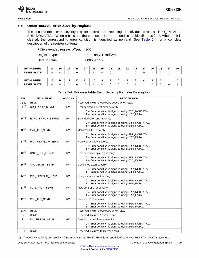
XIO2213B
www.ti.com SCPS210F –OCTOBER 2008–REVISED MAY 2013
5.5 Uncorrectable Error Severity Register
The uncorrectable error severity register controls the reporting of individual errors as ERR_FATAL orERR_NONFATAL. When a bit is set, the corresponding error condition is identified as fatal. When a bit iscleared, the corresponding error condition is identified as nonfatal. See Table 5-4 for a completedescription of the register contents.
PCIe extended register offset: 10Ch
Register type: Read only, Read/Write
Default value: 0006 2011h
BIT NUMBER 31 30 29 28 27 26 25 24 23 22 21 20 19 18 17 16
RESET STATE 0 0 0 0 0 0 0 0 0 0 0 0 0 1 1 0
BIT NUMBER 15 14 13 12 11 10 9 8 7 6 5 4 3 2 1 0
RESET STATE 0 0 1 0 0 0 0 0 0 0 1 1 0 0 0 1
Table 5-4. Uncorrectable Error Severity Register Description
BIT FIELD NAME ACCESS DESCRIPTION
31:21 RSVD R Reserved. Returns 000 0000 0000b when read.
20 (1) UR_ERROR_SEVRO RW Unsupported request error severity
0 = Error condition is signaled using ERR_NONFATAL.1 = Error condition is signaled using ERR_FATAL.
19(1) ECRC_ERROR_SEVRR RW Extended CRC error severity
0 = Error condition is signaled using ERR_NONFATAL.1 = Error condition is signaled using ERR_FATAL.
18(1) MAL_TLP_SEVR RW Malformed TLP severity
0 = Error condition is signaled using ERR_NONFATAL.1 = Error condition is signaled using ERR_FATAL.
17(1) RX_OVERFLOW_SEVR RW Receiver overflow severity
0 = Error condition is signaled using ERR_NONFATAL.1 = Error condition is signaled using ERR_FATAL.
16(1) UNXP_CPL_SEVRP RW Unexpected completion severity
0 = Error condition is signaled using ERR_NONFATAL.1 = Error condition is signaled using ERR_FATAL.
15(1) CPL_ABORT_SEVR RW Completed abort severity
0 = Error condition is signaled using ERR_NONFATAL.1 = Error condition is signaled using ERR_FATAL.
14(1) CPL_TIMEOUT_SEVR RW Completion time-out severity
0 = Error condition is signaled using ERR_NONFATAL.1 = Error condition is signaled using ERR_FATAL.
13(1) FC_ERROR_SEVR RW Flow control error severity
0 = Error condition is signaled using ERR_NONFATAL.1 = Error condition is signaled using ERR_FATAL.
12(1) PSN_TLP_SEVR RW Poisoned TLP severity
0 = Error condition is signaled using ERR_NONFATAL.1 = Error condition is signaled using ERR_FATAL.
11:6 RSVD R Reserved. Returns 000 000b when read.
5 RSVD R Reserved. Returns 1h when read.
4(1) DLL_ERROR_SEVR RW Data link protocol error severity
0 = Error condition is signaled using ERR_NONFATAL.1 = Error condition is signaled using ERR_FATAL.
3:1 RSVD R Reserved. Returns 000b when read.
(1) These bits shall only be reset by a fundamental reset (FRST). FRST is asserted (low) whenever PERST or GRST is asserted.
Copyright © 2008–2013, Texas Instruments Incorporated PCIe Extended Configuration Space 99Submit Documentation FeedbackProduct Folder Links: XIO2213B

XIO2213B
SCPS210F –OCTOBER 2008–REVISED MAY 2013 www.ti.com
Table 5-4. Uncorrectable Error Severity Register Description (continued)
BIT FIELD NAME ACCESS DESCRIPTION
0 RSVD R Reserved. Returns 1h when read.
100 PCIe Extended Configuration Space Copyright © 2008–2013, Texas Instruments Incorporated
Submit Documentation FeedbackProduct Folder Links: XIO2213B
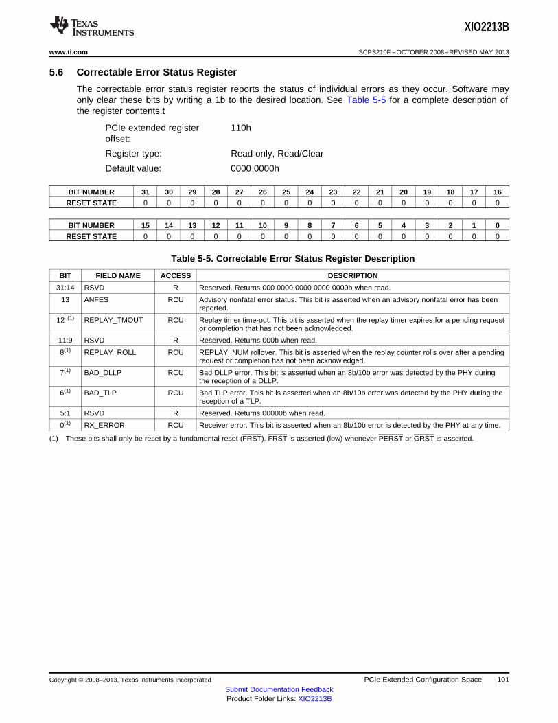
XIO2213B
www.ti.com SCPS210F –OCTOBER 2008–REVISED MAY 2013
5.6 Correctable Error Status Register
The correctable error status register reports the status of individual errors as they occur. Software mayonly clear these bits by writing a 1b to the desired location. See Table 5-5 for a complete description ofthe register contents.t
PCIe extended register 110hoffset:
Register type: Read only, Read/Clear
Default value: 0000 0000h
BIT NUMBER 31 30 29 28 27 26 25 24 23 22 21 20 19 18 17 16
RESET STATE 0 0 0 0 0 0 0 0 0 0 0 0 0 0 0 0
BIT NUMBER 15 14 13 12 11 10 9 8 7 6 5 4 3 2 1 0
RESET STATE 0 0 0 0 0 0 0 0 0 0 0 0 0 0 0 0
Table 5-5. Correctable Error Status Register Description
BIT FIELD NAME ACCESS DESCRIPTION
31:14 RSVD R Reserved. Returns 000 0000 0000 0000 0000b when read.
13 ANFES RCU Advisory nonfatal error status. This bit is asserted when an advisory nonfatal error has beenreported.
12 (1) REPLAY_TMOUT RCU Replay timer time-out. This bit is asserted when the replay timer expires for a pending requestor completion that has not been acknowledged.
11:9 RSVD R Reserved. Returns 000b when read.
8(1) REPLAY_ROLL RCU REPLAY_NUM rollover. This bit is asserted when the replay counter rolls over after a pendingrequest or completion has not been acknowledged.
7(1) BAD_DLLP RCU Bad DLLP error. This bit is asserted when an 8b/10b error was detected by the PHY duringthe reception of a DLLP.
6(1) BAD_TLP RCU Bad TLP error. This bit is asserted when an 8b/10b error was detected by the PHY during thereception of a TLP.
5:1 RSVD R Reserved. Returns 00000b when read.
0(1) RX_ERROR RCU Receiver error. This bit is asserted when an 8b/10b error is detected by the PHY at any time.
(1) These bits shall only be reset by a fundamental reset (FRST). FRST is asserted (low) whenever PERST or GRST is asserted.
Copyright © 2008–2013, Texas Instruments Incorporated PCIe Extended Configuration Space 101Submit Documentation FeedbackProduct Folder Links: XIO2213B
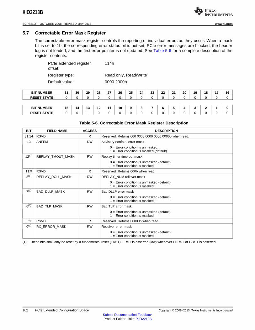
XIO2213B
SCPS210F –OCTOBER 2008–REVISED MAY 2013 www.ti.com
5.7 Correctable Error Mask Register
The correctable error mask register controls the reporting of individual errors as they occur. When a maskbit is set to 1b, the corresponding error status bit is not set, PCIe error messages are blocked, the headerlog is not loaded, and the first error pointer is not updated. See Table 5-6 for a complete description of theregister contents.
PCIe extended register 114hoffset:
Register type: Read only, Read/Write
Default value: 0000 2000h
BIT NUMBER 31 30 29 28 27 26 25 24 23 22 21 20 19 18 17 16
RESET STATE 0 0 0 0 0 0 0 0 0 0 0 0 0 0 0 0
BIT NUMBER 15 14 13 12 11 10 9 8 7 6 5 4 3 2 1 0
RESET STATE 0 0 1 0 0 0 0 0 0 0 0 0 0 0 0 0
Table 5-6. Correctable Error Mask Register Description
BIT FIELD NAME ACCESS DESCRIPTION
31:14 RSVD R Reserved. Returns 000 0000 0000 0000 0000b when read.
13 ANFEM RW Advisory nonfatal error mask
0 = Error condition is unmasked.1 = Error condition is masked (default).
12 (1) REPLAY_TMOUT_MASK RW Replay timer time-out mask
0 = Error condition is unmasked (default).1 = Error condition is masked.
11:9 RSVD R Reserved. Returns 000b when read.
8(1) REPLAY_ROLL_MASK RW REPLAY_NUM rollover mask
0 = Error condition is unmasked (default).1 = Error condition is masked.
7(1) BAD_DLLP_MASK RW Bad DLLP error mask
0 = Error condition is unmasked (default).1 = Error condition is masked.
6(1) BAD_TLP_MASK RW Bad TLP error mask
0 = Error condition is unmasked (default).1 = Error condition is masked.
5:1 RSVD R Reserved. Returns 00000b when read.
0(1) RX_ERROR_MASK RW Receiver error mask
0 = Error condition is unmasked (default).1 = Error condition is masked.
(1) These bits shall only be reset by a fundamental reset (FRST). FRST is asserted (low) whenever PERST or GRST is asserted.
102 PCIe Extended Configuration Space Copyright © 2008–2013, Texas Instruments Incorporated
Submit Documentation FeedbackProduct Folder Links: XIO2213B
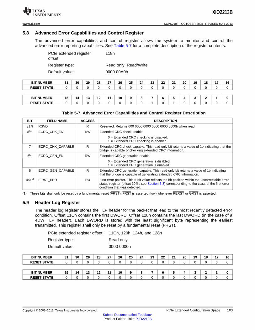
XIO2213B
www.ti.com SCPS210F –OCTOBER 2008–REVISED MAY 2013
5.8 Advanced Error Capabilities and Control Register
The advanced error capabilities and control register allows the system to monitor and control theadvanced error reporting capabilities. See Table 5-7 for a complete description of the register contents.
PCIe extended register 118hoffset:
Register type: Read only, Read/Write
Default value: 0000 00A0h
BIT NUMBER 31 30 29 28 27 26 25 24 23 22 21 20 19 18 17 16
RESET STATE 0 0 0 0 0 0 0 0 0 0 0 0 0 0 0 0
BIT NUMBER 15 14 13 12 11 10 9 8 7 6 5 4 3 2 1 0
RESET STATE 0 0 0 0 0 0 0 0 1 0 1 0 0 0 0 0
Table 5-7. Advanced Error Capabilities and Control Register Description
BIT FIELD NAME ACCESS DESCRIPTION
31:9 RSVD R Reserved. Returns 000 0000 0000 0000 0000 0000b when read.
8 (1) ECRC_CHK_EN RW Extended CRC check enable
0 = Extended CRC checking is disabled.1 = Extended CRC checking is enabled.
7 ECRC_CHK_CAPABLE R Extended CRC check capable. This read-only bit returns a value of 1b indicating that thebridge is capable of checking extended CRC information.
6(1) ECRC_GEN_EN RW Extended CRC generation enable
0 = Extended CRC generation is disabled.1 = Extended CRC generation is enabled.
5 ECRC_GEN_CAPABLE R Extended CRC generation capable. This read-only bit returns a value of 1b indicatingthat the bridge is capable of generating extended CRC information.
4:0(1) FIRST_ERR RU First error pointer. This 5-bit value reflects the bit position within the uncorrectable errorstatus register (offset 104h, see Section 5.3) corresponding to the class of the first errorcondition that was detected.
(1) These bits shall only be reset by a fundamental reset (FRST). FRST is asserted (low) whenever PERST or GRST is asserted.
5.9 Header Log Register
The header log register stores the TLP header for the packet that lead to the most recently detected errorcondition. Offset 11Ch contains the first DWORD. Offset 128h contains the last DWORD (in the case of a4DW TLP header). Each DWORD is stored with the least significant byte representing the earliesttransmitted. This register shall only be reset by a fundamental reset (FRST).
PCIe extended register offset: 11Ch, 120h, 124h, and 128h
Register type: Read only
Default value: 0000 0000h
BIT NUMBER 31 30 29 28 27 26 25 24 23 22 21 20 19 18 17 16
RESET STATE 0 0 0 0 0 0 0 0 0 0 0 0 0 0 0 0
BIT NUMBER 15 14 13 12 11 10 9 8 7 6 5 4 3 2 1 0
RESET STATE 0 0 0 0 0 0 0 0 0 0 0 0 0 0 0 0
Copyright © 2008–2013, Texas Instruments Incorporated PCIe Extended Configuration Space 103Submit Documentation FeedbackProduct Folder Links: XIO2213B
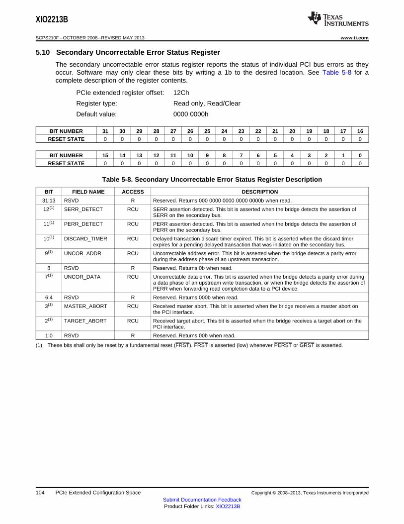
XIO2213B
SCPS210F –OCTOBER 2008–REVISED MAY 2013 www.ti.com
5.10 Secondary Uncorrectable Error Status Register
The secondary uncorrectable error status register reports the status of individual PCI bus errors as theyoccur. Software may only clear these bits by writing a 1b to the desired location. See Table 5-8 for acomplete description of the register contents.
PCIe extended register offset: 12Ch
Register type: Read only, Read/Clear
Default value: 0000 0000h
BIT NUMBER 31 30 29 28 27 26 25 24 23 22 21 20 19 18 17 16
RESET STATE 0 0 0 0 0 0 0 0 0 0 0 0 0 0 0 0
BIT NUMBER 15 14 13 12 11 10 9 8 7 6 5 4 3 2 1 0
RESET STATE 0 0 0 0 0 0 0 0 0 0 0 0 0 0 0 0
Table 5-8. Secondary Uncorrectable Error Status Register Description
BIT FIELD NAME ACCESS DESCRIPTION
31:13 RSVD R Reserved. Returns 000 0000 0000 0000 0000b when read.
12 (1) SERR_DETECT RCU SERR assertion detected. This bit is asserted when the bridge detects the assertion ofSERR on the secondary bus.
11(1) PERR_DETECT RCU PERR assertion detected. This bit is asserted when the bridge detects the assertion ofPERR on the secondary bus.
10(1) DISCARD_TIMER RCU Delayed transaction discard timer expired. This bit is asserted when the discard timerexpires for a pending delayed transaction that was initiated on the secondary bus.
9(1) UNCOR_ADDR RCU Uncorrectable address error. This bit is asserted when the bridge detects a parity errorduring the address phase of an upstream transaction.
8 RSVD R Reserved. Returns 0b when read.
7(1) UNCOR_DATA RCU Uncorrectable data error. This bit is asserted when the bridge detects a parity error duringa data phase of an upstream write transaction, or when the bridge detects the assertion ofPERR when forwarding read completion data to a PCI device.
6:4 RSVD R Reserved. Returns 000b when read.
3(1) MASTER_ABORT RCU Received master abort. This bit is asserted when the bridge receives a master abort onthe PCI interface.
2(1) TARGET_ABORT RCU Received target abort. This bit is asserted when the bridge receives a target abort on thePCI interface.
1:0 RSVD R Reserved. Returns 00b when read.
(1) These bits shall only be reset by a fundamental reset (FRST). FRST is asserted (low) whenever PERST or GRST is asserted.
104 PCIe Extended Configuration Space Copyright © 2008–2013, Texas Instruments Incorporated
Submit Documentation FeedbackProduct Folder Links: XIO2213B
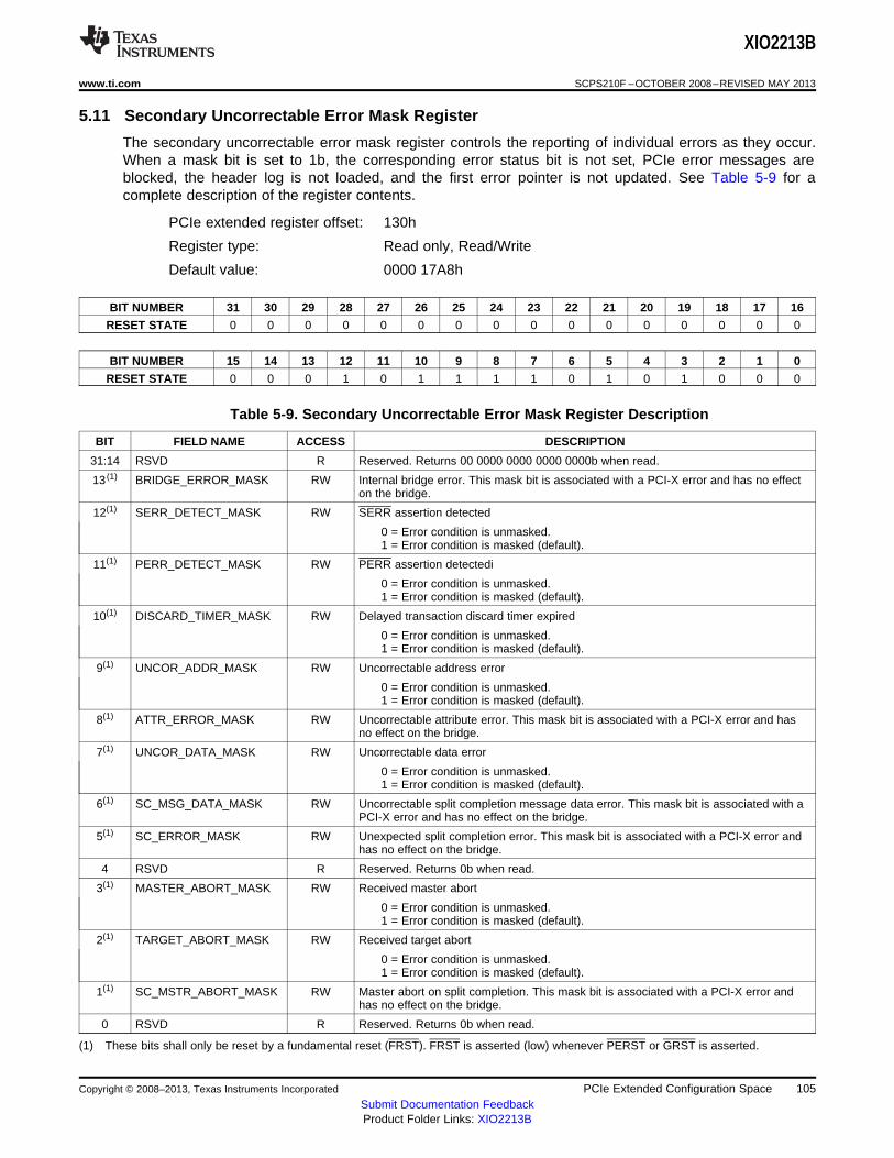
XIO2213B
www.ti.com SCPS210F –OCTOBER 2008–REVISED MAY 2013
5.11 Secondary Uncorrectable Error Mask Register
The secondary uncorrectable error mask register controls the reporting of individual errors as they occur.When a mask bit is set to 1b, the corresponding error status bit is not set, PCIe error messages areblocked, the header log is not loaded, and the first error pointer is not updated. See Table 5-9 for acomplete description of the register contents.
PCIe extended register offset: 130h
Register type: Read only, Read/Write
Default value: 0000 17A8h
BIT NUMBER 31 30 29 28 27 26 25 24 23 22 21 20 19 18 17 16
RESET STATE 0 0 0 0 0 0 0 0 0 0 0 0 0 0 0 0
BIT NUMBER 15 14 13 12 11 10 9 8 7 6 5 4 3 2 1 0
RESET STATE 0 0 0 1 0 1 1 1 1 0 1 0 1 0 0 0
Table 5-9. Secondary Uncorrectable Error Mask Register Description
BIT FIELD NAME ACCESS DESCRIPTION
31:14 RSVD R Reserved. Returns 00 0000 0000 0000 0000b when read.
13 (1) BRIDGE_ERROR_MASK RW Internal bridge error. This mask bit is associated with a PCI-X error and has no effecton the bridge.
12(1) SERR_DETECT_MASK RW SERR assertion detected
0 = Error condition is unmasked.1 = Error condition is masked (default).
11(1) PERR_DETECT_MASK RW PERR assertion detectedi
0 = Error condition is unmasked.1 = Error condition is masked (default).
10(1) DISCARD_TIMER_MASK RW Delayed transaction discard timer expired
0 = Error condition is unmasked.1 = Error condition is masked (default).
9(1) UNCOR_ADDR_MASK RW Uncorrectable address error
0 = Error condition is unmasked.1 = Error condition is masked (default).
8(1) ATTR_ERROR_MASK RW Uncorrectable attribute error. This mask bit is associated with a PCI-X error and hasno effect on the bridge.
7(1) UNCOR_DATA_MASK RW Uncorrectable data error
0 = Error condition is unmasked.1 = Error condition is masked (default).
6(1) SC_MSG_DATA_MASK RW Uncorrectable split completion message data error. This mask bit is associated with aPCI-X error and has no effect on the bridge.
5(1) SC_ERROR_MASK RW Unexpected split completion error. This mask bit is associated with a PCI-X error andhas no effect on the bridge.
4 RSVD R Reserved. Returns 0b when read.
3(1) MASTER_ABORT_MASK RW Received master abort
0 = Error condition is unmasked.1 = Error condition is masked (default).
2(1) TARGET_ABORT_MASK RW Received target abort
0 = Error condition is unmasked.1 = Error condition is masked (default).
1(1) SC_MSTR_ABORT_MASK RW Master abort on split completion. This mask bit is associated with a PCI-X error andhas no effect on the bridge.
0 RSVD R Reserved. Returns 0b when read.
(1) These bits shall only be reset by a fundamental reset (FRST). FRST is asserted (low) whenever PERST or GRST is asserted.
Copyright © 2008–2013, Texas Instruments Incorporated PCIe Extended Configuration Space 105Submit Documentation FeedbackProduct Folder Links: XIO2213B
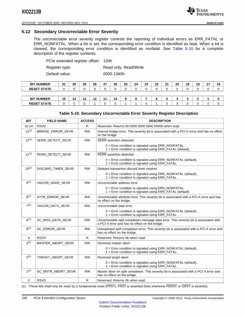
XIO2213B
SCPS210F –OCTOBER 2008–REVISED MAY 2013 www.ti.com
5.12 Secondary Uncorrectable Error Severity
The uncorrectable error severity register controls the reporting of individual errors as ERR_FATAL orERR_NONFATAL. When a bit is set, the corresponding error condition is identified as fatal. When a bit iscleared, the corresponding error condition is identified as nonfatal. See Table 5-10 for a completedescription of the register contents.
PCIe extended register offset: 134h
Register type: Read only, Read/Write
Default value: 0000 1340h
BIT NUMBER 31 30 29 28 27 26 25 24 23 22 21 20 19 18 17 16
RESET STATE 0 0 0 0 0 0 0 0 0 0 0 0 0 0 0 0
BIT NUMBER 15 14 13 12 11 10 9 8 7 6 5 4 3 2 1 0
RESET STATE 0 0 0 1 0 0 1 1 0 1 0 0 0 0 0 0
Table 5-10. Secondary Uncorrectable Error Severity Register Description
BIT FIELD NAME ACCESS DESCRIPTION
31:14 RSVD R Reserved. Returns 00 0000 0000 0000 0000b when read.
13 (1) BRIDGE_ERROR_SEVR RW Internal bridge error. This severity bit is associated with a PCI-X error and has no effecton the bridge.
12(1) SERR_DETECT_SEVR RW SERR assertion detected
0 = Error condition is signaled using ERR_NONFATAL.1 = Error condition is signaled using ERR_FATAL (default).
11(1) PERR_DETECT_SEVR RW PERR assertion detected
0 = Error condition is signaled using ERR_NONFATAL (default).1 = Error condition is signaled using ERR_FATAL.
10(1) DISCARD_TIMER_SEVR RW Delayed transaction discard timer expired
0 = Error condition is signaled using ERR_NONFATAL (default).1 = Error condition is signaled using ERR_FATAL.
9(1) UNCOR_ADDR_SEVR RW Uncorrectable address error
0 = Error condition is signaled using ERR_NONFATAL.1 = Error condition is signaled using ERR_FATAL (default).
8(1) ATTR_ERROR_SEVR RW Uncorrectable attribute error. This severity bit is associated with a PCI-X error and hasno effect on the bridge.
7(1) UNCOR_DATA_SEVR RW Uncorrectable data error
0 = Error condition is signaled using ERR_NONFATAL (default).1 = Error condition is signaled using ERR_FATAL.
6(1) SC_MSG_DATA_SEVR RW Uncorrectable split completion message data error. This severity bit is associated witha PCI-X error and has no effect on the bridge.
5(1) SC_ERROR_SEVR RW Unexpected split completion error. This severity bit is associated with a PCI-X error andhas no effect on the bridge.
4 RSVD R Reserved. Returns 0b when read.
3(1) MASTER_ABORT_SEVR RW Received master abort
0 = Error condition is signaled using ERR_NONFATAL (default).1 = Error condition is signaled using ERR_FATAL.
2(1) TARGET_ABORT_SEVR RW Received target abort
0 = Error condition is signaled using ERR_NONFATAL (default).1 = Error condition is signaled using ERR_FATAL.
1(1) SC_MSTR_ABORT_SEVR RW Master abort on split completion. This severity bit is associated with a PCI-X error andhas no effect on the bridge.
0 RSVD R Reserved. Returns 0b when read.
(1) These bits shall only be reset by a fundamental reset (FRST). FRST is asserted (low) whenever PERST or GRST is asserted.
106 PCIe Extended Configuration Space Copyright © 2008–2013, Texas Instruments Incorporated
Submit Documentation FeedbackProduct Folder Links: XIO2213B
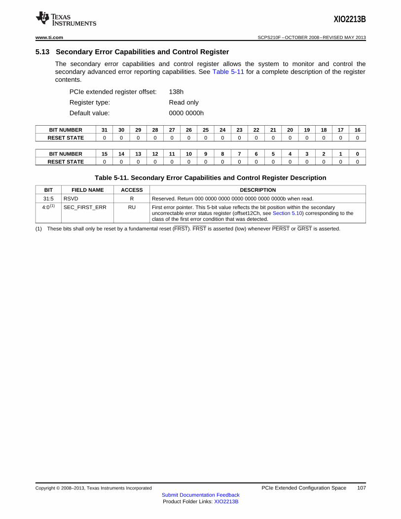
XIO2213B
www.ti.com SCPS210F –OCTOBER 2008–REVISED MAY 2013
5.13 Secondary Error Capabilities and Control Register
The secondary error capabilities and control register allows the system to monitor and control thesecondary advanced error reporting capabilities. See Table 5-11 for a complete description of the registercontents.
PCIe extended register offset: 138h
Register type: Read only
Default value: 0000 0000h
BIT NUMBER 31 30 29 28 27 26 25 24 23 22 21 20 19 18 17 16
RESET STATE 0 0 0 0 0 0 0 0 0 0 0 0 0 0 0 0
BIT NUMBER 15 14 13 12 11 10 9 8 7 6 5 4 3 2 1 0
RESET STATE 0 0 0 0 0 0 0 0 0 0 0 0 0 0 0 0
Table 5-11. Secondary Error Capabilities and Control Register Description
BIT FIELD NAME ACCESS DESCRIPTION
31:5 RSVD R Reserved. Return 000 0000 0000 0000 0000 0000 0000b when read.
4:0 (1) SEC_FIRST_ERR RU First error pointer. This 5-bit value reflects the bit position within the secondaryuncorrectable error status register (offset12Ch, see Section 5.10) corresponding to theclass of the first error condition that was detected.
(1) These bits shall only be reset by a fundamental reset (FRST). FRST is asserted (low) whenever PERST or GRST is asserted.
Copyright © 2008–2013, Texas Instruments Incorporated PCIe Extended Configuration Space 107Submit Documentation FeedbackProduct Folder Links: XIO2213B
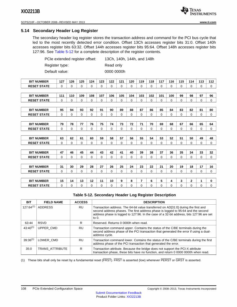
XIO2213B
SCPS210F –OCTOBER 2008–REVISED MAY 2013 www.ti.com
5.14 Secondary Header Log Register
The secondary header log register stores the transaction address and command for the PCI bus cycle thatled to the most recently detected error condition. Offset 13Ch accesses register bits 31:0. Offset 140haccesses register bits 63:32. Offset 144h accesses register bits 95:64. Offset 148h accesses register bits127:96. See Table 5-12 for a complete description of the register contents.
PCIe extended register offset: 13Ch, 140h, 144h, and 148h
Register type: Read only
Default value: 0000 0000h
BIT NUMBER 127 126 125 124 123 122 121 120 119 118 117 116 115 114 113 112
RESET STATE 0 0 0 0 0 0 0 0 0 0 0 0 0 0 0 0
BIT NUMBER 111 110 109 108 107 106 105 104 103 102 101 100 99 98 97 96
RESET STATE 0 0 0 0 0 0 0 0 0 0 0 0 0 0 0 0
BIT NUMBER 95 94 93 92 91 90 89 88 87 86 85 84 83 82 81 80
RESET STATE 0 0 0 0 0 0 0 0 0 0 0 0 0 0 0 0
BIT NUMBER 79 78 77 76 75 74 73 72 71 70 69 68 67 66 65 64
RESET STATE 0 0 0 0 0 0 0 0 0 0 0 0 0 0 0 0
BIT NUMBER 63 62 61 60 59 58 57 56 55 54 53 52 51 50 49 48
RESET STATE 0 0 0 0 0 0 0 0 0 0 0 0 0 0 0 0
BIT NUMBER 47 46 45 44 43 42 41 40 39 38 37 36 35 34 33 32
RESET STATE 0 0 0 0 0 0 0 0 0 0 0 0 0 0 0 0
BIT NUMBER 31 30 29 28 27 26 25 24 23 22 21 20 19 18 17 16
RESET STATE 0 0 0 0 0 0 0 0 0 0 0 0 0 0 0 0
BIT NUMBER 15 14 13 12 11 10 9 8 7 6 5 4 3 2 1 0
RESET STATE 0 0 0 0 0 0 0 0 0 0 0 0 0 0 0 0
Table 5-12. Secondary Header Log Register Description
BIT FIELD NAME ACCESS DESCRIPTION
127:64 (1) ADDRESS RU Transaction address. The 64-bit value transferred on AD[31:0] during the first andsecond address phases. The first address phase is logged to 95:64 and the secondaddress phase is logged to 127:96. In the case of a 32-bit address, bits 127:96 are setto 0.
63:44 RSVD R Reserved. Returns 0 0000h when read.
43:40(1) UPPER_CMD RU Transaction command upper. Contains the status of the C/BE terminals during thesecond address phase of the PCI transaction that generated the error if using a dual-address cycle.
39:36(1) LOWER_CMD RU Transaction command lower. Contains the status of the C/BE terminals during the firstaddress phase of the PCI transaction that generated the error.
35:0 TRANS_ATTRIBUTE R Transaction attribute. Because the bridge does not support the PCI-X attributetransaction phase, these bits have no function, and return 0 0000 0000h when read.
(1) These bits shall only be reset by a fundamental reset (FRST). FRST is asserted (low) whenever PERST or GRST is asserted.
108 PCIe Extended Configuration Space Copyright © 2008–2013, Texas Instruments Incorporated
Submit Documentation FeedbackProduct Folder Links: XIO2213B
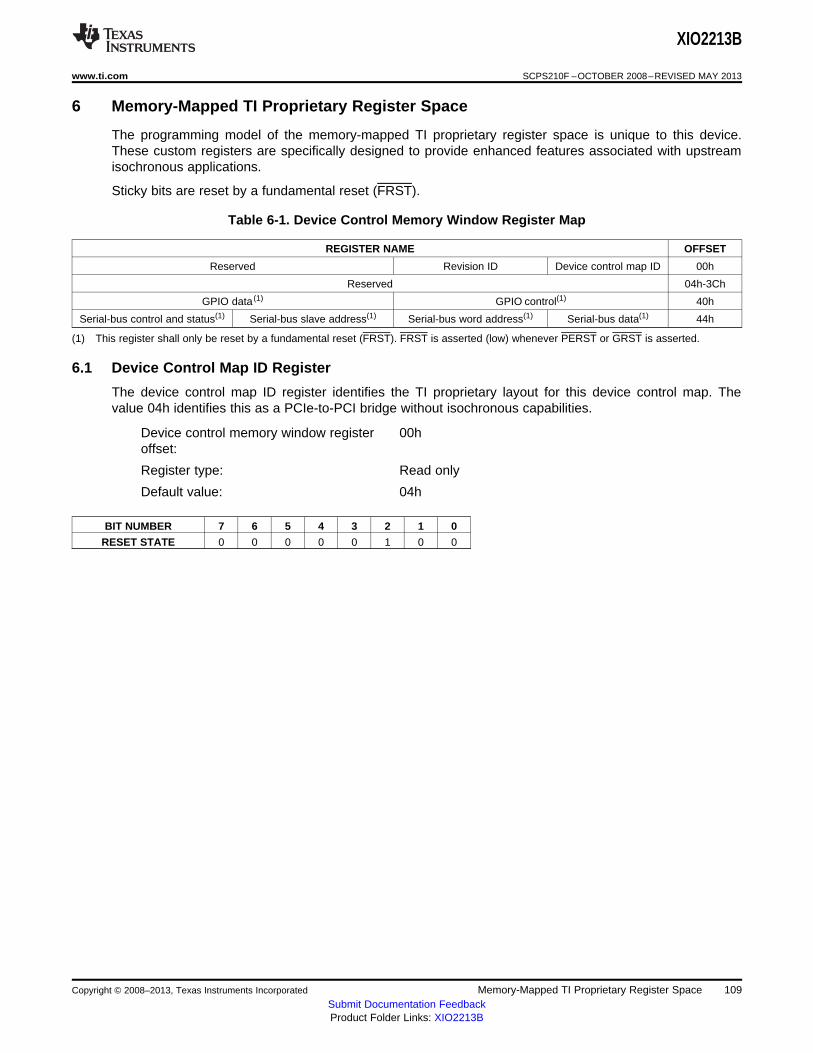
XIO2213B
www.ti.com SCPS210F –OCTOBER 2008–REVISED MAY 2013
6 Memory-Mapped TI Proprietary Register Space
The programming model of the memory-mapped TI proprietary register space is unique to this device.These custom registers are specifically designed to provide enhanced features associated with upstreamisochronous applications.
Sticky bits are reset by a fundamental reset (FRST).
Table 6-1. Device Control Memory Window Register Map
REGISTER NAME OFFSET
Reserved Revision ID Device control map ID 00h
Reserved 04h-3Ch
GPIO data (1) GPIO control(1) 40h
Serial-bus control and status(1) Serial-bus slave address(1) Serial-bus word address(1) Serial-bus data(1) 44h
(1) This register shall only be reset by a fundamental reset (FRST). FRST is asserted (low) whenever PERST or GRST is asserted.
6.1 Device Control Map ID Register
The device control map ID register identifies the TI proprietary layout for this device control map. Thevalue 04h identifies this as a PCIe-to-PCI bridge without isochronous capabilities.
Device control memory window register 00hoffset:
Register type: Read only
Default value: 04h
BIT NUMBER 7 6 5 4 3 2 1 0
RESET STATE 0 0 0 0 0 1 0 0
Copyright © 2008–2013, Texas Instruments Incorporated Memory-Mapped TI Proprietary Register Space 109Submit Documentation FeedbackProduct Folder Links: XIO2213B
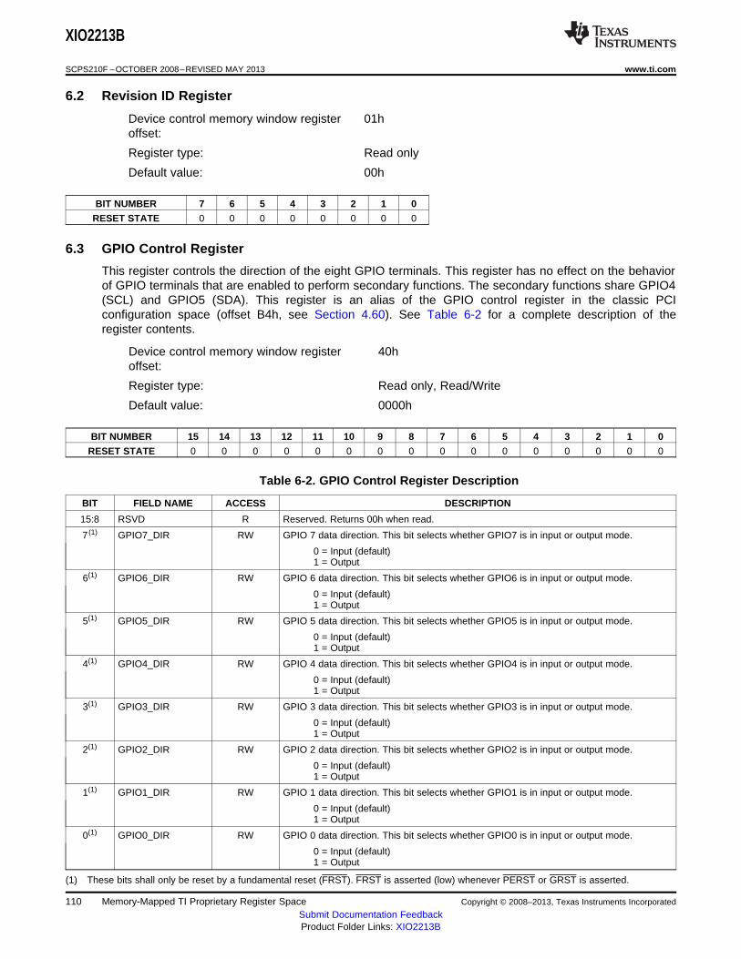
XIO2213B
SCPS210F –OCTOBER 2008–REVISED MAY 2013 www.ti.com
6.2 Revision ID Register
Device control memory window register 01hoffset:
Register type: Read only
Default value: 00h
BIT NUMBER 7 6 5 4 3 2 1 0
RESET STATE 0 0 0 0 0 0 0 0
6.3 GPIO Control Register
This register controls the direction of the eight GPIO terminals. This register has no effect on the behaviorof GPIO terminals that are enabled to perform secondary functions. The secondary functions share GPIO4(SCL) and GPIO5 (SDA). This register is an alias of the GPIO control register in the classic PCIconfiguration space (offset B4h, see Section 4.60). See Table 6-2 for a complete description of theregister contents.
Device control memory window register 40hoffset:
Register type: Read only, Read/Write
Default value: 0000h
BIT NUMBER 15 14 13 12 11 10 9 8 7 6 5 4 3 2 1 0
RESET STATE 0 0 0 0 0 0 0 0 0 0 0 0 0 0 0 0
Table 6-2. GPIO Control Register Description
BIT FIELD NAME ACCESS DESCRIPTION
15:8 RSVD R Reserved. Returns 00h when read.
7 (1) GPIO7_DIR RW GPIO 7 data direction. This bit selects whether GPIO7 is in input or output mode.
0 = Input (default)1 = Output
6(1) GPIO6_DIR RW GPIO 6 data direction. This bit selects whether GPIO6 is in input or output mode.
0 = Input (default)1 = Output
5(1) GPIO5_DIR RW GPIO 5 data direction. This bit selects whether GPIO5 is in input or output mode.
0 = Input (default)1 = Output
4(1) GPIO4_DIR RW GPIO 4 data direction. This bit selects whether GPIO4 is in input or output mode.
0 = Input (default)1 = Output
3(1) GPIO3_DIR RW GPIO 3 data direction. This bit selects whether GPIO3 is in input or output mode.
0 = Input (default)1 = Output
2(1) GPIO2_DIR RW GPIO 2 data direction. This bit selects whether GPIO2 is in input or output mode.
0 = Input (default)1 = Output
1(1) GPIO1_DIR RW GPIO 1 data direction. This bit selects whether GPIO1 is in input or output mode.
0 = Input (default)1 = Output
0(1) GPIO0_DIR RW GPIO 0 data direction. This bit selects whether GPIO0 is in input or output mode.
0 = Input (default)1 = Output
(1) These bits shall only be reset by a fundamental reset (FRST). FRST is asserted (low) whenever PERST or GRST is asserted.
110 Memory-Mapped TI Proprietary Register Space Copyright © 2008–2013, Texas Instruments Incorporated
Submit Documentation FeedbackProduct Folder Links: XIO2213B
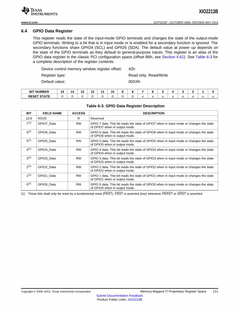
XIO2213B
www.ti.com SCPS210F –OCTOBER 2008–REVISED MAY 2013
6.4 GPIO Data Register
This register reads the state of the input-mode GPIO terminals and changes the state of the output-modeGPIO terminals. Writing to a bit that is in input mode or is enabled for a secondary function is ignored. Thesecondary functions share GPIO4 (SCL) and GPIO5 (SDA). The default value at power up depends onthe state of the GPIO terminals as they default to general-purpose inputs. This register is an alias of theGPIO data register in the classic PCI configuration space (offset B6h, see Section 4.61). See Table 6-3 fora complete description of the register contents.
Device control memory window register offset: 42h
Register type: Read only, Read/Write
Default value: 00XXh
BIT NUMBER 15 14 13 12 11 10 9 8 7 6 5 4 3 2 1 0
RESET STATE 0 0 0 0 0 0 0 0 x x x x x x x x
Table 6-3. GPIO Data Register Description
BIT FIELD NAME ACCESS DESCRIPTION
15:8 RSVD R Reserved
7 (1) GPIO7_Data RW GPIO 7 data. This bit reads the state of GPIO7 when in input mode or changes the stateof GPIO7 when in output mode.
6(1) GPIO6_Data RW GPIO 6 data. This bit reads the state of GPIO6 when in input mode or changes the stateof GPIO6 when in output mode.
5(1) GPIO5_Data RW GPIO 5 data. This bit reads the state of GPIO5 when in input mode or changes the stateof GPIO5 when in output mode.
4(1) GPIO4_Data RW GPIO 4 data. This bit reads the state of GPIO4 when in input mode or changes the stateof GPIO4 when in output mode.
3(1) GPIO3_Data RW GPIO 3 data. This bit reads the state of GPIO3 when in input mode or changes the stateof GPIO3 when in output mode.
2(1) GPIO2_Data RW GPIO 2 data. This bit reads the state of GPIO2 when in input mode or changes the stateof GPIO2 when in output mode.
1(1) GPIO1_Data RW GPIO 1 data. This bit reads the state of GPIO1 when in input mode or changes the stateof GPIO1 when in output mode.
0(1) GPIO0_Data RW GPIO 0 data. This bit reads the state of GPIO0 when in input mode or changes the stateof GPIO0 when in output mode.
(1) These bits shall only be reset by a fundamental reset (FRST). FRST is asserted (low) whenever PERST or GRST is asserted.
Copyright © 2008–2013, Texas Instruments Incorporated Memory-Mapped TI Proprietary Register Space 111Submit Documentation FeedbackProduct Folder Links: XIO2213B
XIO2213B
SCPS210F –OCTOBER 2008–REVISED MAY 2013 www.ti.com
6.5 Serial-Bus Data Register
The serial-bus data register is used to read and write data on the serial-bus interface. When writing datato the serial bus, this register must be written before writing to the serial-bus address register to initiate thecycle. When reading data from the serial bus, this register will contain the data read after the REQBUSY(bit 5 serial-bus control register) bit is cleared. This register is an alias for the serial-bus data register inthe PCI header. This register shall only be reset by FRST.
Device control memory window register offset: 44h
Register type: Read/Write
Default value: 00h
BIT NUMBER 7 6 5 4 3 2 1 0
RESET STATE 0 0 0 0 0 0 0 1
6.6 Serial-Bus Word Address Register
The value written to the serial-bus index register represents the byte address of the byte being read orwritten from the serial-bus device. The serial-bus index register must be written before the before initiatinga serial bus cycle by writing to the serial-bus slave address register. This register is an alias for the serial-bus index register in the PCI header. This register shall only be reset by FRST.
Device control memory window register offset: 45h
Register type: Read/Write
Default value: 00h
BIT NUMBER 7 6 5 4 3 2 1 0
RESET STATE 0 0 0 0 0 0 0 0
6.7 Serial-Bus Slave Address Register
The serial-bus slave address register is used to indicate the address of the device being targeted by theserial-bus cycle. This register also indicates if the cycle will be a read or a write cycle. Writing to thisregister initiates the cycle on the serial interface. This register is an alias for the serial-bus slave addressregister in the PCI header.
Device control memory window register offset: 46h
Register type: Read/Write
Default value: 00h
BIT NUMBER 7 6 5 4 3 2 1 0
RESET STATE 0 0 0 0 0 0 0 0
Table 6-4. Serial-Bus Slave Address Register Descriptions
BIT FIELD NAME ACCESS DESCRIPTION
7:1 (1) SLAVE_ADDR RW Serial-bus slave address. This 7-bit field is the slave address for a serial-bus read or writetransaction. The default value for this field is 000 0000b.
0(1) RW_CMD RW Read/write command. This bit determines if the serial-bus cycle is a read or a write cycle.
0 = A single-byte write is requested (default) .1 = A single-byte read is requested.
(1) These bits shall only be reset by a fundamental reset (FRST). FRST is asserted (low) whenever PERST or GRST is asserted.
112 Memory-Mapped TI Proprietary Register Space Copyright © 2008–2013, Texas Instruments Incorporated
Submit Documentation FeedbackProduct Folder Links: XIO2213B
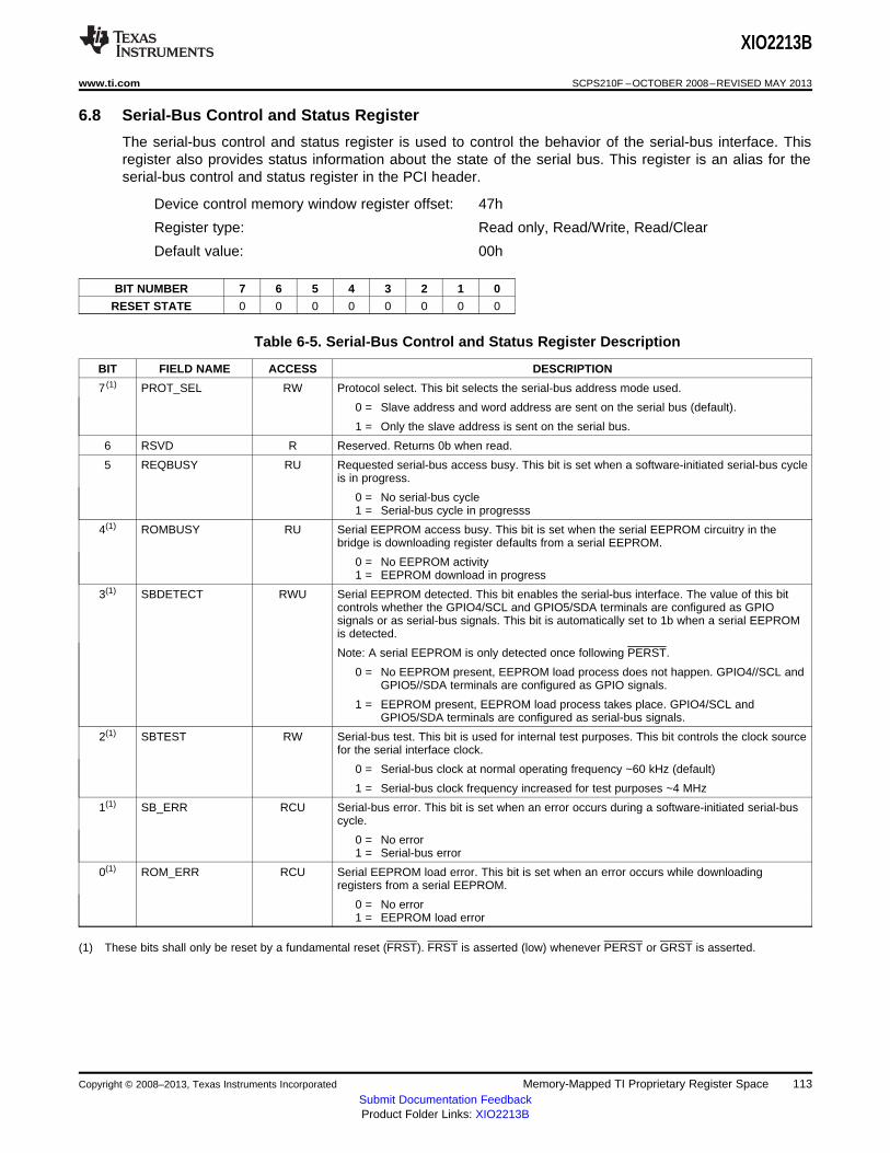
XIO2213B
www.ti.com SCPS210F –OCTOBER 2008–REVISED MAY 2013
6.8 Serial-Bus Control and Status Register
The serial-bus control and status register is used to control the behavior of the serial-bus interface. Thisregister also provides status information about the state of the serial bus. This register is an alias for theserial-bus control and status register in the PCI header.
Device control memory window register offset: 47h
Register type: Read only, Read/Write, Read/Clear
Default value: 00h
BIT NUMBER 7 6 5 4 3 2 1 0
RESET STATE 0 0 0 0 0 0 0 0
Table 6-5. Serial-Bus Control and Status Register Description
BIT FIELD NAME ACCESS DESCRIPTION
7 (1) PROT_SEL RW Protocol select. This bit selects the serial-bus address mode used.
0 = Slave address and word address are sent on the serial bus (default).
1 = Only the slave address is sent on the serial bus.
6 RSVD R Reserved. Returns 0b when read.
5 REQBUSY RU Requested serial-bus access busy. This bit is set when a software-initiated serial-bus cycleis in progress.
0 = No serial-bus cycle1 = Serial-bus cycle in progresss
4(1) ROMBUSY RU Serial EEPROM access busy. This bit is set when the serial EEPROM circuitry in thebridge is downloading register defaults from a serial EEPROM.
0 = No EEPROM activity1 = EEPROM download in progress
3(1) SBDETECT RWU Serial EEPROM detected. This bit enables the serial-bus interface. The value of this bitcontrols whether the GPIO4/SCL and GPIO5/SDA terminals are configured as GPIOsignals or as serial-bus signals. This bit is automatically set to 1b when a serial EEPROMis detected.
Note: A serial EEPROM is only detected once following PERST.
0 = No EEPROM present, EEPROM load process does not happen. GPIO4//SCL andGPIO5//SDA terminals are configured as GPIO signals.
1 = EEPROM present, EEPROM load process takes place. GPIO4/SCL andGPIO5/SDA terminals are configured as serial-bus signals.
2(1) SBTEST RW Serial-bus test. This bit is used for internal test purposes. This bit controls the clock sourcefor the serial interface clock.
0 = Serial-bus clock at normal operating frequency ~60 kHz (default)
1 = Serial-bus clock frequency increased for test purposes ~4 MHz
1(1) SB_ERR RCU Serial-bus error. This bit is set when an error occurs during a software-initiated serial-buscycle.
0 = No error1 = Serial-bus error
0(1) ROM_ERR RCU Serial EEPROM load error. This bit is set when an error occurs while downloadingregisters from a serial EEPROM.
0 = No error1 = EEPROM load error
(1) These bits shall only be reset by a fundamental reset (FRST). FRST is asserted (low) whenever PERST or GRST is asserted.
Copyright © 2008–2013, Texas Instruments Incorporated Memory-Mapped TI Proprietary Register Space 113Submit Documentation FeedbackProduct Folder Links: XIO2213B
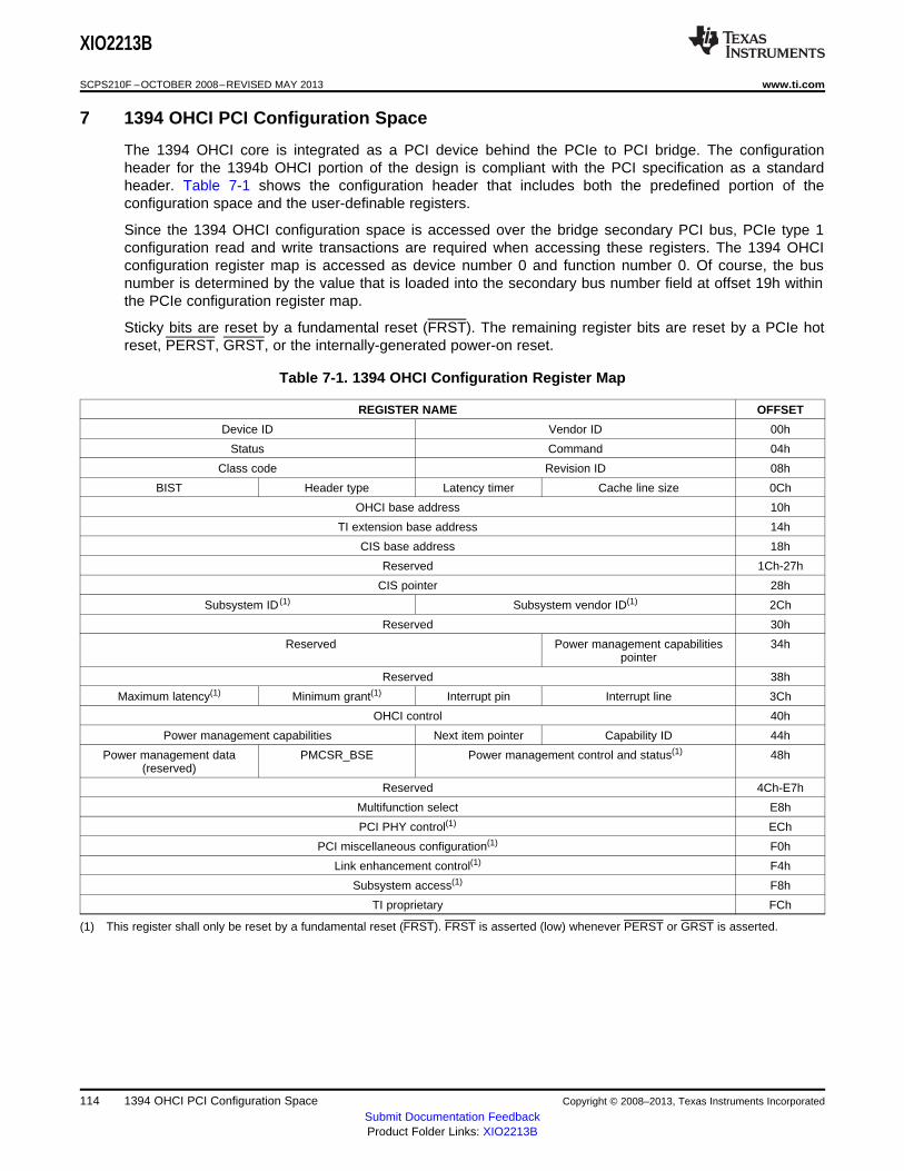
XIO2213B
SCPS210F –OCTOBER 2008–REVISED MAY 2013 www.ti.com
7 1394 OHCI PCI Configuration Space
The 1394 OHCI core is integrated as a PCI device behind the PCIe to PCI bridge. The configurationheader for the 1394b OHCI portion of the design is compliant with the PCI specification as a standardheader. Table 7-1 shows the configuration header that includes both the predefined portion of theconfiguration space and the user-definable registers.
Since the 1394 OHCI configuration space is accessed over the bridge secondary PCI bus, PCIe type 1configuration read and write transactions are required when accessing these registers. The 1394 OHCIconfiguration register map is accessed as device number 0 and function number 0. Of course, the busnumber is determined by the value that is loaded into the secondary bus number field at offset 19h withinthe PCIe configuration register map.
Sticky bits are reset by a fundamental reset (FRST). The remaining register bits are reset by a PCIe hotreset, PERST, GRST, or the internally-generated power-on reset.
Table 7-1. 1394 OHCI Configuration Register Map
REGISTER NAME OFFSET
Device ID Vendor ID 00h
Status Command 04h
Class code Revision ID 08h
BIST Header type Latency timer Cache line size 0Ch
OHCI base address 10h
TI extension base address 14h
CIS base address 18h
Reserved 1Ch-27h
CIS pointer 28h
Subsystem ID (1) Subsystem vendor ID(1) 2Ch
Reserved 30h
Reserved Power management capabilities 34hpointer
Reserved 38h
Maximum latency(1) Minimum grant(1) Interrupt pin Interrupt line 3Ch
OHCI control 40h
Power management capabilities Next item pointer Capability ID 44h
Power management data PMCSR_BSE Power management control and status(1) 48h(reserved)
Reserved 4Ch-E7h
Multifunction select E8h
PCI PHY control(1) ECh
PCI miscellaneous configuration(1) F0h
Link enhancement control(1) F4h
Subsystem access(1) F8h
TI proprietary FCh
(1) This register shall only be reset by a fundamental reset (FRST). FRST is asserted (low) whenever PERST or GRST is asserted.
114 1394 OHCI PCI Configuration Space Copyright © 2008–2013, Texas Instruments Incorporated
Submit Documentation FeedbackProduct Folder Links: XIO2213B
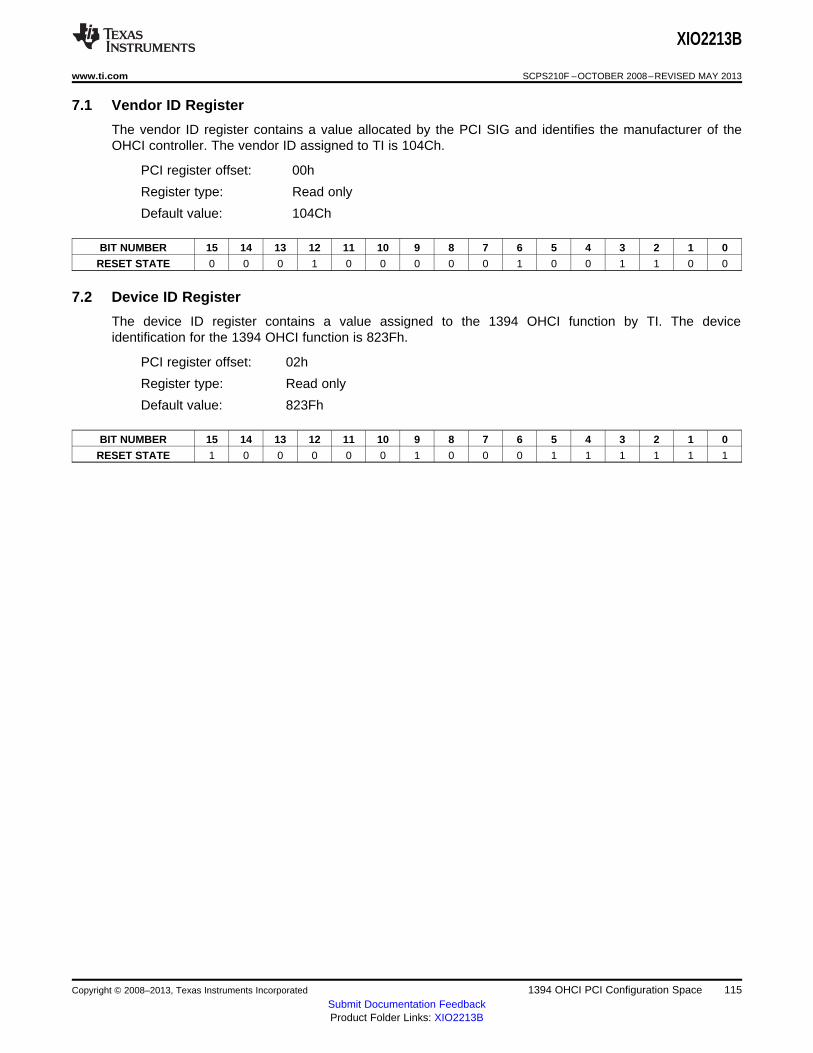
XIO2213B
www.ti.com SCPS210F –OCTOBER 2008–REVISED MAY 2013
7.1 Vendor ID Register
The vendor ID register contains a value allocated by the PCI SIG and identifies the manufacturer of theOHCI controller. The vendor ID assigned to TI is 104Ch.
PCI register offset: 00h
Register type: Read only
Default value: 104Ch
BIT NUMBER 15 14 13 12 11 10 9 8 7 6 5 4 3 2 1 0
RESET STATE 0 0 0 1 0 0 0 0 0 1 0 0 1 1 0 0
7.2 Device ID Register
The device ID register contains a value assigned to the 1394 OHCI function by TI. The deviceidentification for the 1394 OHCI function is 823Fh.
PCI register offset: 02h
Register type: Read only
Default value: 823Fh
BIT NUMBER 15 14 13 12 11 10 9 8 7 6 5 4 3 2 1 0
RESET STATE 1 0 0 0 0 0 1 0 0 0 1 1 1 1 1 1
Copyright © 2008–2013, Texas Instruments Incorporated 1394 OHCI PCI Configuration Space 115Submit Documentation FeedbackProduct Folder Links: XIO2213B
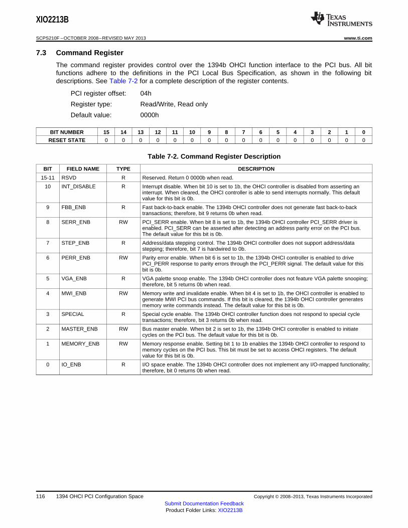
XIO2213B
SCPS210F –OCTOBER 2008–REVISED MAY 2013 www.ti.com
7.3 Command Register
The command register provides control over the 1394b OHCI function interface to the PCI bus. All bitfunctions adhere to the definitions in the PCI Local Bus Specification, as shown in the following bitdescriptions. See Table 7-2 for a complete description of the register contents.
PCI register offset: 04h
Register type: Read/Write, Read only
Default value: 0000h
BIT NUMBER 15 14 13 12 11 10 9 8 7 6 5 4 3 2 1 0
RESET STATE 0 0 0 0 0 0 0 0 0 0 0 0 0 0 0 0
Table 7-2. Command Register Description
BIT FIELD NAME TYPE DESCRIPTION
15-11 RSVD R Reserved. Return 0 0000b when read.
10 INT_DISABLE R Interrupt disable. When bit 10 is set to 1b, the OHCI controller is disabled from asserting aninterrupt. When cleared, the OHCI controller is able to send interrupts normally. This defaultvalue for this bit is 0b.
9 FBB_ENB R Fast back-to-back enable. The 1394b OHCI controller does not generate fast back-to-backtransactions; therefore, bit 9 returns 0b when read.
8 SERR_ENB RW PCI_SERR enable. When bit 8 is set to 1b, the 1394b OHCI controller PCI_SERR driver isenabled. PCI_SERR can be asserted after detecting an address parity error on the PCI bus.The default value for this bit is 0b.
7 STEP_ENB R Address/data stepping control. The 1394b OHCI controller does not support address/datastepping; therefore, bit 7 is hardwired to 0b.
6 PERR_ENB RW Parity error enable. When bit 6 is set to 1b, the 1394b OHCI controller is enabled to drivePCI_PERR response to parity errors through the PCI_PERR signal. The default value for thisbit is 0b.
5 VGA_ENB R VGA palette snoop enable. The 1394b OHCI controller does not feature VGA palette snooping;therefore, bit 5 returns 0b when read.
4 MWI_ENB RW Memory write and invalidate enable. When bit 4 is set to 1b, the OHCI controller is enabled togenerate MWI PCI bus commands. If this bit is cleared, the 1394b OHCI controller generatesmemory write commands instead. The default value for this bit is 0b.
3 SPECIAL R Special cycle enable. The 1394b OHCI controller function does not respond to special cycletransactions; therefore, bit 3 returns 0b when read.
2 MASTER_ENB RW Bus master enable. When bit 2 is set to 1b, the 1394b OHCI controller is enabled to initiatecycles on the PCI bus. The default value for this bit is 0b.
1 MEMORY_ENB RW Memory response enable. Setting bit 1 to 1b enables the 1394b OHCI controller to respond tomemory cycles on the PCI bus. This bit must be set to access OHCI registers. The defaultvalue for this bit is 0b.
0 IO_ENB R I/O space enable. The 1394b OHCI controller does not implement any I/O-mapped functionality;therefore, bit 0 returns 0b when read.
116 1394 OHCI PCI Configuration Space Copyright © 2008–2013, Texas Instruments Incorporated
Submit Documentation FeedbackProduct Folder Links: XIO2213B
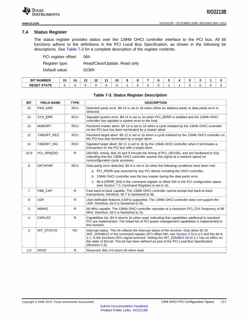
XIO2213B
www.ti.com SCPS210F –OCTOBER 2008–REVISED MAY 2013
7.4 Status Register
The status register provides status over the 1394b OHCI controller interface to the PCI bus. All bitfunctions adhere to the definitions in the PCI Local Bus Specification, as shown in the following bitdescriptions. See Table 7-3 for a complete description of the register contents.
PCI register offset: 06h
Register type: Read/Clear/Update, Read only
Default value: 0230h
BIT NUMBER 15 14 13 12 11 10 9 8 7 6 5 4 3 2 1 0
RESET STATE 0 0 0 0 0 0 1 0 0 0 1 1 0 0 0 0
Table 7-3. Status Register Description
BIT FIELD NAME TYPE DESCRIPTION
15 PAR_ERR RCU Detected parity error. Bit 15 is set to 1b when either an address parity or data parity error isdetected.
14 SYS_ERR RCU Signaled system error. Bit 14 is set to 1b when PCI_SERR is enabled and the 1394b OHCIcontroller has signaled a system error to the host.
13 MABORT RCU Received master abort. Bit 13 is set to 1b when a cycle initiated by the 1394b OHCI controlleron the PCI bus has been terminated by a master abort.
12 TABORT_REC RCU Received target abort. Bit 12 is set to 1b when a cycle initiated by the 1394b OHCI controller onthe PCI bus was terminated by a target abort.
11 TABORT_SIG RCU Signaled target abort. Bit 11 is set to 1b by the 1394b OHCI controller when it terminates atransaction on the PCI bus with a target abort.
10-9 PCI_SPEEDO R DEVSEL timing. Bits 10 and 9 encode the timing of PCI_DEVSEL and are hardwired to 01b,indicating that the 1394b OHCI controller asserts this signal at a medium speed onnonconfiguration cycle accesses.
8 DATAPAR RCU Data parity error detected. Bit 8 is set to 1b when the following conditions have been met:
a. PCI_PERR was asserted by any PCI device including the OHCI controller.
b. 1394b OHCI controller was the bus master during the data parity error.
c. Bit 6 (PERR_EN) in the command register at offset 04h in the PCI configuration space(see Section 7.3, Command Register) is set to 1b.
7 FBB_CAP R Fast back-to-back capable. The 1394b OHCI controller cannot accept fast back-to-backtransactions; therefore, bit 7 is hardwired to 0b.
6 UDF R User-definable features (UDFs) supported. The 1394b OHCI controller does not support theUDF; therefore, bit 6 is hardwired to 0b.
5 66MHZ R 66-MHz capable. The 1394b OHCI controller operates at a maximum PCI_CLK frequency of 66MHz; therefore, bit 5 is hardwired to 1b.
4 CAPLIST R Capabilities list. Bit 4 returns 1b when read, indicating that capabilities additional to standardPCI are implemented. The linked list of PCI power-management capabilities is implemented inthis function.
3 INT_STATUS RU Interrupt status. This bit reflects the interrupt status of the function. Only when bit 10(INT_DISABLE) in the command register (PCI offset 04h, see Section 4.3) is a 0 and this bit isa 1, is the functions INTx signal asserted. Setting the INT_DISABLE bit to a 1 has no effect onthe state of this bit. This bit has been defined as part of the PCI Local Bus Specification(Revision 2.3).
2-0 RSVD R Reserved. Bits 3-0 return 0h when read.
Copyright © 2008–2013, Texas Instruments Incorporated 1394 OHCI PCI Configuration Space 117Submit Documentation FeedbackProduct Folder Links: XIO2213B
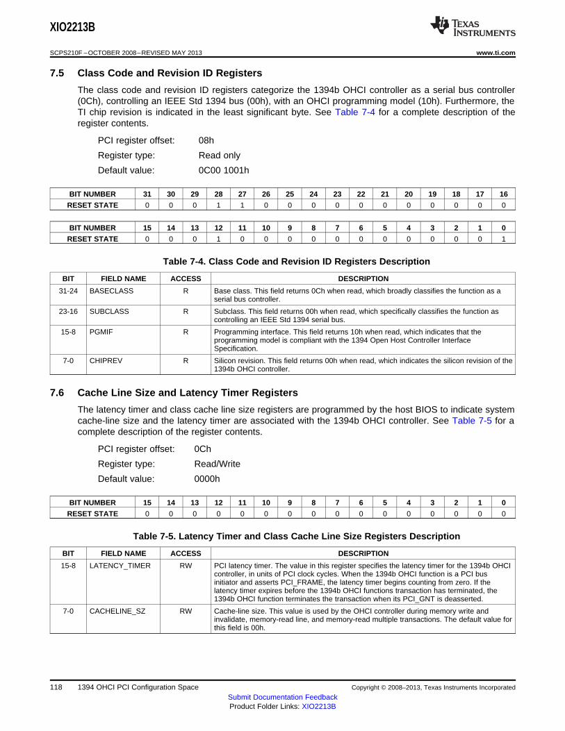
XIO2213B
SCPS210F –OCTOBER 2008–REVISED MAY 2013 www.ti.com
7.5 Class Code and Revision ID Registers
The class code and revision ID registers categorize the 1394b OHCI controller as a serial bus controller(0Ch), controlling an IEEE Std 1394 bus (00h), with an OHCI programming model (10h). Furthermore, theTI chip revision is indicated in the least significant byte. See Table 7-4 for a complete description of theregister contents.
PCI register offset: 08h
Register type: Read only
Default value: 0C00 1001h
BIT NUMBER 31 30 29 28 27 26 25 24 23 22 21 20 19 18 17 16
RESET STATE 0 0 0 1 1 0 0 0 0 0 0 0 0 0 0 0
BIT NUMBER 15 14 13 12 11 10 9 8 7 6 5 4 3 2 1 0
RESET STATE 0 0 0 1 0 0 0 0 0 0 0 0 0 0 0 1
Table 7-4. Class Code and Revision ID Registers Description
BIT FIELD NAME ACCESS DESCRIPTION
31-24 BASECLASS R Base class. This field returns 0Ch when read, which broadly classifies the function as aserial bus controller.
23-16 SUBCLASS R Subclass. This field returns 00h when read, which specifically classifies the function ascontrolling an IEEE Std 1394 serial bus.
15-8 PGMIF R Programming interface. This field returns 10h when read, which indicates that theprogramming model is compliant with the 1394 Open Host Controller InterfaceSpecification.
7-0 CHIPREV R Silicon revision. This field returns 00h when read, which indicates the silicon revision of the1394b OHCI controller.
7.6 Cache Line Size and Latency Timer Registers
The latency timer and class cache line size registers are programmed by the host BIOS to indicate systemcache-line size and the latency timer are associated with the 1394b OHCI controller. See Table 7-5 for acomplete description of the register contents.
PCI register offset: 0Ch
Register type: Read/Write
Default value: 0000h
BIT NUMBER 15 14 13 12 11 10 9 8 7 6 5 4 3 2 1 0
RESET STATE 0 0 0 0 0 0 0 0 0 0 0 0 0 0 0 0
Table 7-5. Latency Timer and Class Cache Line Size Registers Description
BIT FIELD NAME ACCESS DESCRIPTION
15-8 LATENCY_TIMER RW PCI latency timer. The value in this register specifies the latency timer for the 1394b OHCIcontroller, in units of PCI clock cycles. When the 1394b OHCI function is a PCI businitiator and asserts PCI_FRAME, the latency timer begins counting from zero. If thelatency timer expires before the 1394b OHCI functions transaction has terminated, the1394b OHCI function terminates the transaction when its PCI_GNT is deasserted.
7-0 CACHELINE_SZ RW Cache-line size. This value is used by the OHCI controller during memory write andinvalidate, memory-read line, and memory-read multiple transactions. The default value forthis field is 00h.
118 1394 OHCI PCI Configuration Space Copyright © 2008–2013, Texas Instruments Incorporated
Submit Documentation FeedbackProduct Folder Links: XIO2213B
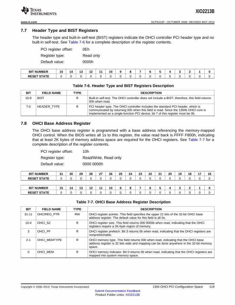
XIO2213B
www.ti.com SCPS210F –OCTOBER 2008–REVISED MAY 2013
7.7 Header Type and BIST Registers
The header type and built-in self-test (BIST) registers indicate the OHCI controller PCI header type and nobuilt-in self-test. See Table 7-6 for a complete description of the register contents.
PCI register offset: 0Eh
Register type: Read only
Default value: 0000h
BIT NUMBER 15 14 13 12 11 10 9 8 7 6 5 4 3 2 1 0
RESET STATE 0 0 0 0 0 0 0 0 0 0 0 0 0 0 0 0
Table 7-6. Header Type and BIST Registers Description
BIT FIELD NAME TYPE DESCRIPTION
15-8 BIST R Built-in self-test. The OHCI controller does not include a BIST; therefore, this field returns00h when read.
7-0 HEADER_TYPE R PCI header type. The OHCI controller includes the standard PCI header, which iscommunicated by returning 00h when this field is read. Since the 1394b OHCI core isimplemented as a single-function PCI device, bit 7 of this register must be 0b.
7.8 OHCI Base Address Register
The OHCI base address register is programmed with a base address referencing the memory-mappedOHCI control. When the BIOS writes all 1s to this register, the value read back is FFFF F800h, indicatingthat at least 2K bytes of memory address space are required for the OHCI registers. See Table 7-7 for acomplete description of the register contents.
PCI register offset: 10h
Register type: Read/Write, Read only
Default value: 0000 0000h
BIT NUMBER 31 30 29 28 27 26 25 24 23 22 21 20 19 18 17 16
RESET STATE 0 0 0 0 0 0 0 0 0 0 0 0 0 0 0 0
BIT NUMBER 15 14 13 12 11 10 9 8 7 6 5 4 3 2 1 0
RESET STATE 0 0 0 0 0 0 0 0 0 0 0 0 0 0 0 0
Table 7-7. OHCI Base Address Register Description
BIT FIELD NAME TYPE DESCRIPTION
31-11 OHCIREG_PTR RW OHCI register pointer. This field specifies the upper 21 bits of the 32-bit OHCI baseaddress register. The default value for this field is all 0s.
10-4 OHCI_SZ R OHCI register size. This field returns 000 0000b when read, indicating that the OHCIregisters require a 2K-byte region of memory.
3 OHCI_PF R OHCI register prefetch. Bit 3 returns 0b when read, indicating that the OHCI registers arenonprefetchable.
2-1 OHCI_MEMTYPE R OHCI memory type. This field returns 00b when read, indicating that the OHCI baseaddress register is 32 bits wide and mapping can be done anywhere in the 32-bit memoryspace.
0 OHCI_MEM R OHCI memory indicator. Bit 0 returns 0b when read, indicating that the OHCI registers aremapped into system memory space.
Copyright © 2008–2013, Texas Instruments Incorporated 1394 OHCI PCI Configuration Space 119Submit Documentation FeedbackProduct Folder Links: XIO2213B
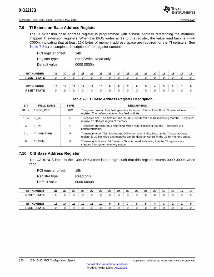
XIO2213B
SCPS210F –OCTOBER 2008–REVISED MAY 2013 www.ti.com
7.9 TI Extension Base Address Register
The TI extension base address register is programmed with a base address referencing the memory-mapped TI extension registers. When the BIOS writes all 1s to this register, the value read back is FFFFC000h, indicating that at least 16K bytes of memory address space are required for the TI registers. SeeTable 7-8 for a complete description of the register contents.
PCI register offset: 14h
Register type: Read/Write, Read only
Default value: 0000 0000h
BIT NUMBER 31 30 29 28 27 26 25 24 23 22 21 20 19 18 17 16
RESET STATE 0 0 0 0 0 0 0 0 0 0 0 0 0 0 0 0
BIT NUMBER 15 14 13 12 11 10 9 8 7 6 5 4 3 2 1 0
RESET STATE 0 0 0 0 0 0 0 0 0 0 0 0 0 0 0 0
Table 7-8. TI Base Address Register Description
BIT FIELD NAME TYPE DESCRIPTION
31-14 TIREG_PTR RW TI register pointer. This field specifies the upper 18 bits of the 32-bit TI base addressregister. The default value for this field is all 0s.
13-4 TI_SZ R TI register size. This field returns 00 0000 0000b when read, indicating that the TI registersrequire a 16K-byte region of memory.
3 TI_PF R TI register prefetch. Bit 3 returns 0b when read, indicating that the TI registers arenonprefetchable.
2-1 TI_MEMTYPE R TI memory type. This field returns 00b when read, indicating that the TI base addressregister is 32 bits wide and mapping can be done anywhere in the 32-bit memory space.
0 TI_MEM R TI memory indicator. Bit 0 returns 0b when read, indicating that the TI registers aremapped into system memory space.
7.10 CIS Base Address Register
The CARDBUS input to the 1394 OHCI core is tied high such that this register returns 0000 0000h whenread.
PCI register offset: 18h
Register type: Read only
Default value: 0000 0000h
BIT NUMBER 31 30 29 28 27 26 25 24 23 22 21 20 19 18 17 16
RESET STATE 0 0 0 0 0 0 0 0 0 0 0 0 0 0 0 0
BIT NUMBER 15 14 13 12 11 10 9 8 7 6 5 4 3 2 1 0
RESET STATE 0 0 0 0 0 0 0 0 0 0 0 0 0 0 0 0
120 1394 OHCI PCI Configuration Space Copyright © 2008–2013, Texas Instruments Incorporated
Submit Documentation FeedbackProduct Folder Links: XIO2213B
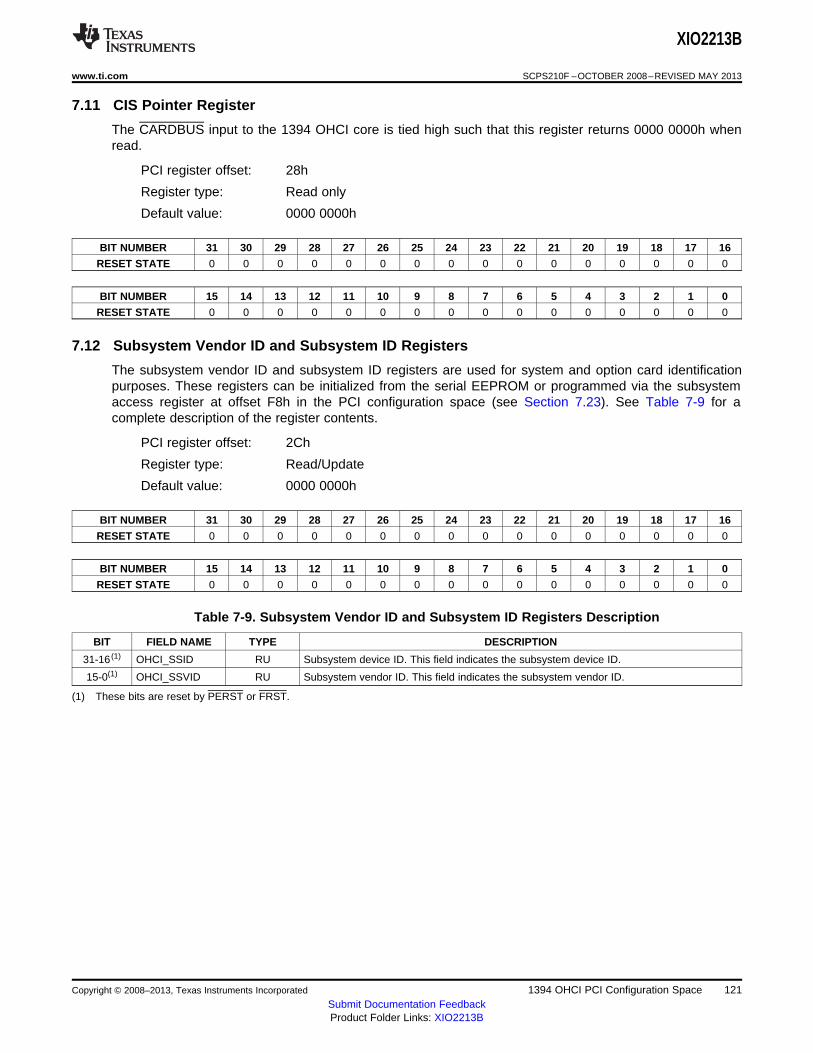
XIO2213B
www.ti.com SCPS210F –OCTOBER 2008–REVISED MAY 2013
7.11 CIS Pointer Register
The CARDBUS input to the 1394 OHCI core is tied high such that this register returns 0000 0000h whenread.
PCI register offset: 28h
Register type: Read only
Default value: 0000 0000h
BIT NUMBER 31 30 29 28 27 26 25 24 23 22 21 20 19 18 17 16
RESET STATE 0 0 0 0 0 0 0 0 0 0 0 0 0 0 0 0
BIT NUMBER 15 14 13 12 11 10 9 8 7 6 5 4 3 2 1 0
RESET STATE 0 0 0 0 0 0 0 0 0 0 0 0 0 0 0 0
7.12 Subsystem Vendor ID and Subsystem ID Registers
The subsystem vendor ID and subsystem ID registers are used for system and option card identificationpurposes. These registers can be initialized from the serial EEPROM or programmed via the subsystemaccess register at offset F8h in the PCI configuration space (see Section 7.23). See Table 7-9 for acomplete description of the register contents.
PCI register offset: 2Ch
Register type: Read/Update
Default value: 0000 0000h
BIT NUMBER 31 30 29 28 27 26 25 24 23 22 21 20 19 18 17 16
RESET STATE 0 0 0 0 0 0 0 0 0 0 0 0 0 0 0 0
BIT NUMBER 15 14 13 12 11 10 9 8 7 6 5 4 3 2 1 0
RESET STATE 0 0 0 0 0 0 0 0 0 0 0 0 0 0 0 0
Table 7-9. Subsystem Vendor ID and Subsystem ID Registers Description
BIT FIELD NAME TYPE DESCRIPTION
31-16 (1) OHCI_SSID RU Subsystem device ID. This field indicates the subsystem device ID.
15-0(1) OHCI_SSVID RU Subsystem vendor ID. This field indicates the subsystem vendor ID.
(1) These bits are reset by PERST or FRST.
Copyright © 2008–2013, Texas Instruments Incorporated 1394 OHCI PCI Configuration Space 121Submit Documentation FeedbackProduct Folder Links: XIO2213B
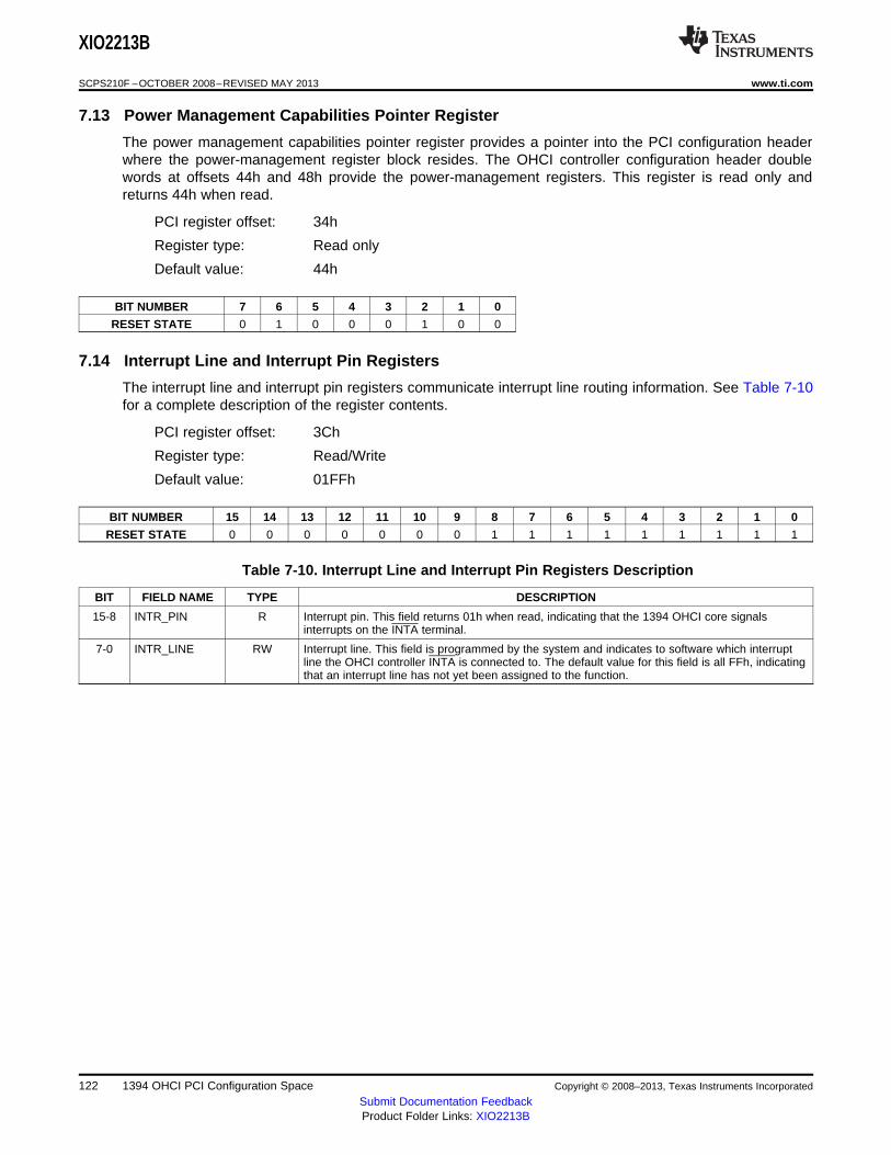
XIO2213B
SCPS210F –OCTOBER 2008–REVISED MAY 2013 www.ti.com
7.13 Power Management Capabilities Pointer Register
The power management capabilities pointer register provides a pointer into the PCI configuration headerwhere the power-management register block resides. The OHCI controller configuration header doublewords at offsets 44h and 48h provide the power-management registers. This register is read only andreturns 44h when read.
PCI register offset: 34h
Register type: Read only
Default value: 44h
BIT NUMBER 7 6 5 4 3 2 1 0
RESET STATE 0 1 0 0 0 1 0 0
7.14 Interrupt Line and Interrupt Pin Registers
The interrupt line and interrupt pin registers communicate interrupt line routing information. See Table 7-10for a complete description of the register contents.
PCI register offset: 3Ch
Register type: Read/Write
Default value: 01FFh
BIT NUMBER 15 14 13 12 11 10 9 8 7 6 5 4 3 2 1 0
RESET STATE 0 0 0 0 0 0 0 1 1 1 1 1 1 1 1 1
Table 7-10. Interrupt Line and Interrupt Pin Registers Description
BIT FIELD NAME TYPE DESCRIPTION
15-8 INTR_PIN R Interrupt pin. This field returns 01h when read, indicating that the 1394 OHCI core signalsinterrupts on the INTA terminal.
7-0 INTR_LINE RW Interrupt line. This field is programmed by the system and indicates to software which interruptline the OHCI controller INTA is connected to. The default value for this field is all FFh, indicatingthat an interrupt line has not yet been assigned to the function.
122 1394 OHCI PCI Configuration Space Copyright © 2008–2013, Texas Instruments Incorporated
Submit Documentation FeedbackProduct Folder Links: XIO2213B
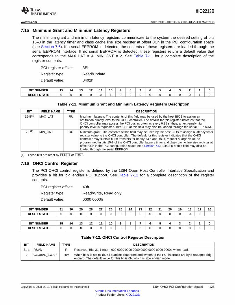
XIO2213B
www.ti.com SCPS210F –OCTOBER 2008–REVISED MAY 2013
7.15 Minimum Grant and Minimum Latency Registers
The minimum grant and minimum latency registers communicate to the system the desired setting of bits15–8 in the latency timer and class cache line size register at offset 0Ch in the PCI configuration space(see Section 7.6). If a serial EEPROM is detected, the contents of these registers are loaded through theserial EEPROM interface. If no serial EEPROM is detected, these registers return a default value thatcorresponds to the MAX_LAT = 4, MIN_GNT = 2. See Table 7-11 for a complete description of theregister contents.
PCI register offset: 3Eh
Register type: Read/Update
Default value: 0402h
BIT NUMBER 15 14 13 12 11 10 9 8 7 6 5 4 3 2 1 0
RESET STATE 0 0 0 0 0 1 0 0 0 0 0 0 0 0 1 0
Table 7-11. Minimum Grant and Minimum Latency Registers Description
BIT FIELD NAME TYPE DESCRIPTION
15-8 (1) MAX_LAT RU Maximum latency. The contents of this field may be used by the host BIOS to assign anarbitration priority level to the OHCI controller. The default for this register indicates that theOHCI controller may access the PCI bus as often as every 0.25 s; thus, an extremely highpriority level is requested. Bits 11-8 of this field may also be loaded through the serial EEPROM.
7-0(1) MIN_GNT RU Minimum grant. The contents of this field may be used by the host BIOS to assign a latency timerregister value to the OHCI controller. The default for this register indicates that the OHCIcontroller may sustain burst transfers for nearly 64 s and, thus, request a large value beprogrammed in bits 15-8 of the OHCI controller latency timer and class cache line size register atoffset 0Ch in the PCI configuration space (see Section 7.6). Bits 3-0 of this field may also beloaded through the serial EEPROM.
(1) These bits are reset by PERST or FRST.
7.16 OHCI Control Register
The PCI OHCI control register is defined by the 1394 Open Host Controller Interface Specification andprovides a bit for big endian PCI support. See Table 7-12 for a complete description of the registercontents.
PCI register offset: 40h
Register type: Read/Write, Read only
Default value: 0000 0000h
BIT NUMBER 31 30 29 28 27 26 25 24 23 22 21 20 19 18 17 16
RESET STATE 0 0 0 0 0 0 0 0 0 0 0 0 0 0 0 0
BIT NUMBER 15 14 13 12 11 10 9 8 7 6 5 4 3 2 1 0
RESET STATE 0 0 0 0 0 0 0 0 0 0 0 0 0 0 0 0
Table 7-12. OHCI Control Register Description
BIT FIELD NAME TYPE DESCRIPTION
31-1 RSVD R Reserved. Bits 31-1 return 000 0000 0000 0000 0000 0000 0000 0000b when read.
0 GLOBAL_SWAP RW When bit 0 is set to 1b, all quadlets read from and written to the PCI interface are byte swapped (bigendian). The default value for this bit is 0b, which is little endian mode.
Copyright © 2008–2013, Texas Instruments Incorporated 1394 OHCI PCI Configuration Space 123Submit Documentation FeedbackProduct Folder Links: XIO2213B
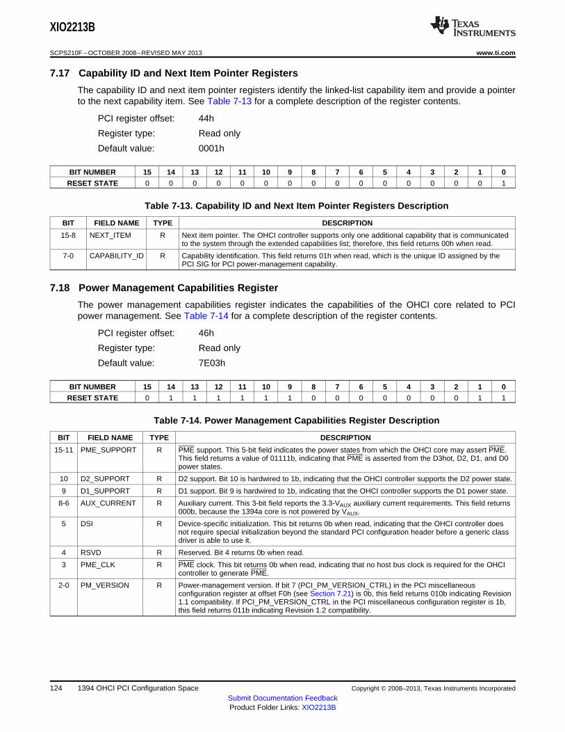
XIO2213B
SCPS210F –OCTOBER 2008–REVISED MAY 2013 www.ti.com
7.17 Capability ID and Next Item Pointer Registers
The capability ID and next item pointer registers identify the linked-list capability item and provide a pointerto the next capability item. See Table 7-13 for a complete description of the register contents.
PCI register offset: 44h
Register type: Read only
Default value: 0001h
BIT NUMBER 15 14 13 12 11 10 9 8 7 6 5 4 3 2 1 0
RESET STATE 0 0 0 0 0 0 0 0 0 0 0 0 0 0 0 1
Table 7-13. Capability ID and Next Item Pointer Registers Description
BIT FIELD NAME TYPE DESCRIPTION
15-8 NEXT_ITEM R Next item pointer. The OHCI controller supports only one additional capability that is communicatedto the system through the extended capabilities list; therefore, this field returns 00h when read.
7-0 CAPABILITY_ID R Capability identification. This field returns 01h when read, which is the unique ID assigned by thePCI SIG for PCI power-management capability.
7.18 Power Management Capabilities Register
The power management capabilities register indicates the capabilities of the OHCI core related to PCIpower management. See Table 7-14 for a complete description of the register contents.
PCI register offset: 46h
Register type: Read only
Default value: 7E03h
BIT NUMBER 15 14 13 12 11 10 9 8 7 6 5 4 3 2 1 0
RESET STATE 0 1 1 1 1 1 1 0 0 0 0 0 0 0 1 1
Table 7-14. Power Management Capabilities Register Description
BIT FIELD NAME TYPE DESCRIPTION
15-11 PME_SUPPORT R PME support. This 5-bit field indicates the power states from which the OHCI core may assert PME.This field returns a value of 01111b, indicating that PME is asserted from the D3hot, D2, D1, and D0power states.
10 D2_SUPPORT R D2 support. Bit 10 is hardwired to 1b, indicating that the OHCI controller supports the D2 power state.
9 D1_SUPPORT R D1 support. Bit 9 is hardwired to 1b, indicating that the OHCI controller supports the D1 power state.
8-6 AUX_CURRENT R Auxiliary current. This 3-bit field reports the 3.3-VAUX auxiliary current requirements. This field returns000b, because the 1394a core is not powered by VAUX.
5 DSI R Device-specific initialization. This bit returns 0b when read, indicating that the OHCI controller doesnot require special initialization beyond the standard PCI configuration header before a generic classdriver is able to use it.
4 RSVD R Reserved. Bit 4 returns 0b when read.
3 PME_CLK R PME clock. This bit returns 0b when read, indicating that no host bus clock is required for the OHCIcontroller to generate PME.
2-0 PM_VERSION R Power-management version. If bit 7 (PCI_PM_VERSION_CTRL) in the PCI miscellaneousconfiguration register at offset F0h (see Section 7.21) is 0b, this field returns 010b indicating Revision1.1 compatibility. If PCI_PM_VERSION_CTRL in the PCI miscellaneous configuration register is 1b,this field returns 011b indicating Revision 1.2 compatibility.
124 1394 OHCI PCI Configuration Space Copyright © 2008–2013, Texas Instruments Incorporated
Submit Documentation FeedbackProduct Folder Links: XIO2213B
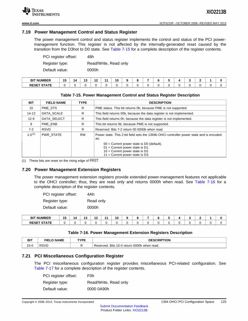
XIO2213B
www.ti.com SCPS210F –OCTOBER 2008–REVISED MAY 2013
7.19 Power Management Control and Status Register
The power management control and status register implements the control and status of the PCI power-management function. This register is not affected by the internally-generated reset caused by thetransition from the D3hot to D0 state. See Table 7-15 for a complete description of the register contents.
PCI register offset: 48h
Register type: Read/Write, Read only
Default value: 0000h
BIT NUMBER 15 14 13 12 11 10 9 8 7 6 5 4 3 2 1 0
RESET STATE 0 0 0 0 0 0 0 0 0 0 0 0 0 0 0 0
Table 7-15. Power Management Control and Status Register Description
BIT FIELD NAME TYPE DESCRIPTION
15 PME_STS R PME status. This bit returns 0b, because PME is not supported.
14-13 DATA_SCALE R This field returns 00b, because the data register is not implemented.
12-9 DATA_SELECT R This field returns 0h, because the data register is not implemented.
8 PME_ENB R This bit returns 0b, because PME is not supported.
7-2 RSVD R Reserved. Bits 7-2 return 00 0000b when read.
1-0 (1) PWR_STATE RW Power state. This 2-bit field sets the 1394b OHCI controller power state and is encodedas:
00 = Current power state is D0 (default).01 = Current power state is D1.10 = Current power state is D2.11 = Current power state is D3.
(1) These bits are reset on the rising edge of PRST.
7.20 Power Management Extension Registers
The power management extension registers provide extended power-management features not applicableto the OHCI controller; thus, they are read only and returns 0000h when read. See Table 7-16 for acomplete description of the register contents.
PCI register offset: 4Ah
Register type: Read only
Default value: 0000h
BIT NUMBER 15 14 13 12 11 10 9 8 7 6 5 4 3 2 1 0
RESET STATE 0 0 0 0 0 0 0 0 0 0 0 0 0 0 0 0
Table 7-16. Power Management Extension Registers Description
BIT FIELD NAME TYPE DESCRIPTION
15-0 RSVD R Reserved. Bits 15-0 return 0000h when read.
7.21 PCI Miscellaneous Configuration Register
The PCI miscellaneous configuration register provides miscellaneous PCI-related configuration. SeeTable 7-17 for a complete description of the register contents.
PCI register offset: F0h
Register type: Read/Write, Read only
Default value: 0000 0A90h
Copyright © 2008–2013, Texas Instruments Incorporated 1394 OHCI PCI Configuration Space 125Submit Documentation FeedbackProduct Folder Links: XIO2213B

XIO2213B
SCPS210F –OCTOBER 2008–REVISED MAY 2013 www.ti.com
BIT NUMBER 31 30 29 28 27 26 25 24 23 22 21 20 19 18 17 16
RESET STATE 0 0 0 0 0 0 0 0 0 0 0 0 0 0 0 0
BIT NUMBER 15 14 13 12 11 10 9 8 7 (1) 6 5 4 3 2 1 0
RESET STATE 0 0 0 0 1 0 1 0 1 0 0 1 0 0 0 0
(1) These bits shall only be reset by a fundamental reset (FRST). FRST is asserted (low) whenever PERST or GRST is asserted.
126 1394 OHCI PCI Configuration Space Copyright © 2008–2013, Texas Instruments Incorporated
Submit Documentation FeedbackProduct Folder Links: XIO2213B
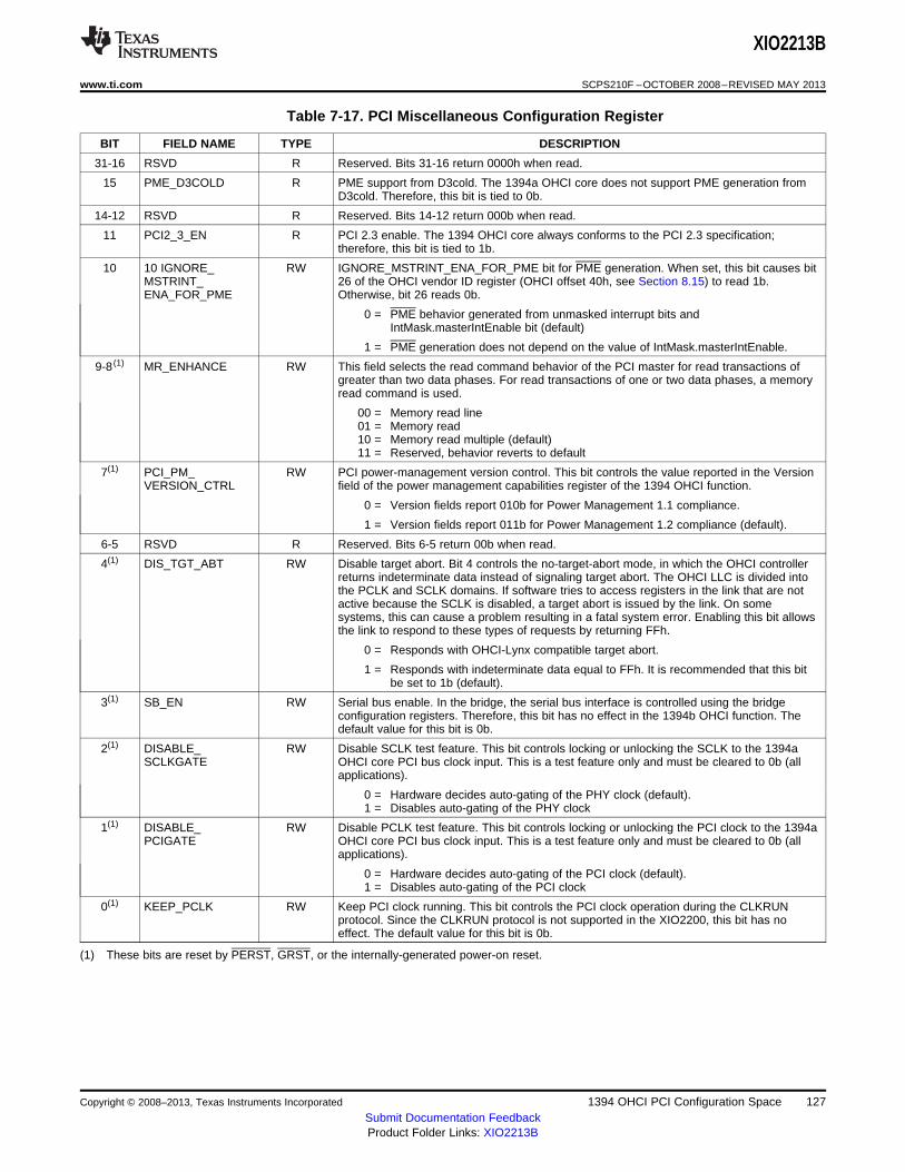
XIO2213B
www.ti.com SCPS210F –OCTOBER 2008–REVISED MAY 2013
Table 7-17. PCI Miscellaneous Configuration Register
BIT FIELD NAME TYPE DESCRIPTION
31-16 RSVD R Reserved. Bits 31-16 return 0000h when read.
15 PME_D3COLD R PME support from D3cold. The 1394a OHCI core does not support PME generation fromD3cold. Therefore, this bit is tied to 0b.
14-12 RSVD R Reserved. Bits 14-12 return 000b when read.
11 PCI2_3_EN R PCI 2.3 enable. The 1394 OHCI core always conforms to the PCI 2.3 specification;therefore, this bit is tied to 1b.
10 10 IGNORE_ RW IGNORE_MSTRINT_ENA_FOR_PME bit for PME generation. When set, this bit causes bitMSTRINT_ 26 of the OHCI vendor ID register (OHCI offset 40h, see Section 8.15) to read 1b.ENA_FOR_PME Otherwise, bit 26 reads 0b.
0 = PME behavior generated from unmasked interrupt bits andIntMask.masterIntEnable bit (default)
1 = PME generation does not depend on the value of IntMask.masterIntEnable.
9-8 (1) MR_ENHANCE RW This field selects the read command behavior of the PCI master for read transactions ofgreater than two data phases. For read transactions of one or two data phases, a memoryread command is used.
00 = Memory read line01 = Memory read10 = Memory read multiple (default)11 = Reserved, behavior reverts to default
7(1) PCI_PM_ RW PCI power-management version control. This bit controls the value reported in the VersionVERSION_CTRL field of the power management capabilities register of the 1394 OHCI function.
0 = Version fields report 010b for Power Management 1.1 compliance.
1 = Version fields report 011b for Power Management 1.2 compliance (default).
6-5 RSVD R Reserved. Bits 6-5 return 00b when read.
4(1) DIS_TGT_ABT RW Disable target abort. Bit 4 controls the no-target-abort mode, in which the OHCI controllerreturns indeterminate data instead of signaling target abort. The OHCI LLC is divided intothe PCLK and SCLK domains. If software tries to access registers in the link that are notactive because the SCLK is disabled, a target abort is issued by the link. On somesystems, this can cause a problem resulting in a fatal system error. Enabling this bit allowsthe link to respond to these types of requests by returning FFh.
0 = Responds with OHCI-Lynx compatible target abort.
1 = Responds with indeterminate data equal to FFh. It is recommended that this bitbe set to 1b (default).
3(1) SB_EN RW Serial bus enable. In the bridge, the serial bus interface is controlled using the bridgeconfiguration registers. Therefore, this bit has no effect in the 1394b OHCI function. Thedefault value for this bit is 0b.
2(1) DISABLE_ RW Disable SCLK test feature. This bit controls locking or unlocking the SCLK to the 1394aSCLKGATE OHCI core PCI bus clock input. This is a test feature only and must be cleared to 0b (all
applications).
0 = Hardware decides auto-gating of the PHY clock (default).1 = Disables auto-gating of the PHY clock
1(1) DISABLE_ RW Disable PCLK test feature. This bit controls locking or unlocking the PCI clock to the 1394aPCIGATE OHCI core PCI bus clock input. This is a test feature only and must be cleared to 0b (all
applications).
0 = Hardware decides auto-gating of the PCI clock (default).1 = Disables auto-gating of the PCI clock
0(1) KEEP_PCLK RW Keep PCI clock running. This bit controls the PCI clock operation during the CLKRUNprotocol. Since the CLKRUN protocol is not supported in the XIO2200, this bit has noeffect. The default value for this bit is 0b.
(1) These bits are reset by PERST, GRST, or the internally-generated power-on reset.
Copyright © 2008–2013, Texas Instruments Incorporated 1394 OHCI PCI Configuration Space 127Submit Documentation FeedbackProduct Folder Links: XIO2213B
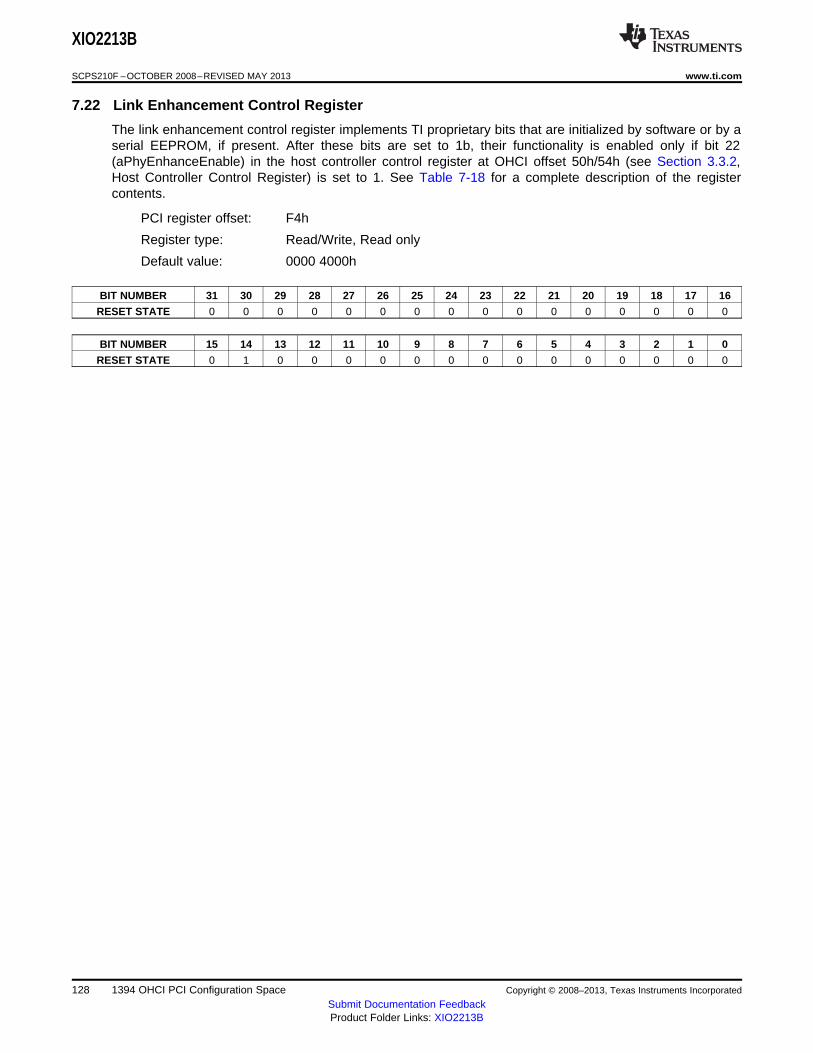
XIO2213B
SCPS210F –OCTOBER 2008–REVISED MAY 2013 www.ti.com
7.22 Link Enhancement Control Register
The link enhancement control register implements TI proprietary bits that are initialized by software or by aserial EEPROM, if present. After these bits are set to 1b, their functionality is enabled only if bit 22(aPhyEnhanceEnable) in the host controller control register at OHCI offset 50h/54h (see Section 3.3.2,Host Controller Control Register) is set to 1. See Table 7-18 for a complete description of the registercontents.
PCI register offset: F4h
Register type: Read/Write, Read only
Default value: 0000 4000h
BIT NUMBER 31 30 29 28 27 26 25 24 23 22 21 20 19 18 17 16
RESET STATE 0 0 0 0 0 0 0 0 0 0 0 0 0 0 0 0
BIT NUMBER 15 14 13 12 11 10 9 8 7 6 5 4 3 2 1 0
RESET STATE 0 1 0 0 0 0 0 0 0 0 0 0 0 0 0 0
128 1394 OHCI PCI Configuration Space Copyright © 2008–2013, Texas Instruments Incorporated
Submit Documentation FeedbackProduct Folder Links: XIO2213B
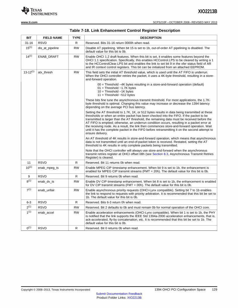
XIO2213B
www.ti.com SCPS210F –OCTOBER 2008–REVISED MAY 2013
Table 7-18. Link Enhancement Control Register Description
BIT FIELD NAME TYPE DESCRIPTION
31-16 RSVD R Reserved. Bits 31-16 return 0000h when read.
15(1) dis_at_pipeline RW Disable AT pipelining. When bit 15 is set to 1b, out-of-order AT pipelining is disabled. Thedefault value for this bit is 0b.
14(1) ENAB_DRAFT RW Enable OHCI 1.2 draft features. When this bit is set, it enables some features beyond theOHCI 1.1 specification. Specifically, this enables HCControl.LPS to be cleared by writing a 1to the HCControlClear.LPS bit and enables the link to set bit 9 in the xfer status field of ARand IR context control registers. This bit can be initialized from an attached EEPROM.
13-12(1) atx_thresh RW This field sets the initial AT threshold value, which is used until the AT FIFO is underrun.When the OHCI controller retries the packet, it uses a 4K-byte threshold, resulting in a store-and-forward operation.
00 = Threshold ~4K bytes resulting in a store-and-forward operation (default)01 = Threshold ~1.7K bytes10 = Threshold ~1K bytes11 = Threshold ~512 bytes
These bits fine tune the asynchronous transmit threshold. For most applications, the 1.7K-byte threshold is optimal. Changing this value may increase or decrease the 1394 latencydepending on the average PCI bus latency.
Setting the AT threshold to 1.7K, 1K, or 512 bytes results in data being transmitted at thesethresholds or when an entire packet has been checked into the FIFO. If the packet to betransmitted is larger than the AT threshold, the remaining data must be received before theAT FIFO is emptied; otherwise, an underrun condition occurs, resulting in a packet error atthe receiving node. As a result, the link then commences store-and-forward operation. Waituntil it has the complete packet in the FIFO before retransmitting it on the second attempt toensure delivery.
An AT threshold of 4K results in store-and-forward operation, which means that asynchronousdata is not transmitted until an end-of-packet token is received. Restated, setting the ATthreshold to 4K results in only complete packets being transmitted.
Note that the OHCI controller will always use store-and-forward when the asynchronoustransmit retries register at OHCI offset 08h (see Section 8.3, Asynchronous Transmit RetriesRegister) is cleared.
11 RSVD R Reserved. Bit 11 returns 0b when read.
10(1) enab_mpeg_ts RW Enable MPEG CIP timestamp enhancement. When bit 9 is set to 1b, the enhancement isenabled for MPEG CIP transmit streams (FMT = 20h). The default value for this bit is 0b.
9 RSVD R Reserved. Bit 9 returns 0b when read.
8(1) enab_dv_ts RW Enable DV CIP timestamp enhancement. When bit 8 is set to 1b, the enhancement is enabledfor DV CIP transmit streams (FMT = 00h). The default value for this bit is 0b.
7(1) enab_unfair RW Enable asynchronous priority requests (OHCI-Lynx compatible). Setting bit 7 to 1b enablesthe link to respond to requests with priority arbitration. It is recommended that this bit be set to1b. The default value for this bit is 0b.
6-3 RSVD R Reserved. Bits 6-3 return 0h when read.
2(1) RSVD RW Reserved. Bit 2 defaults to 0b and must remain 0b for normal operation of the OHCI core.
1(1) enab_accel RW Enable acceleration enhancements (OHCI-Lynx compatible). When bit 1 is set to 1b, the PHYis notified that the link supports the IEEE Std 1394a-2000 acceleration enhancements, that is,ack-accelerated, fly-by concatenation, etc. It is recommended that this bit be set to 1b. Thedefault value for this bit is 0b.
0(1) RSVD R Reserved. Bit 0 returns 0b when read.
Copyright © 2008–2013, Texas Instruments Incorporated 1394 OHCI PCI Configuration Space 129Submit Documentation FeedbackProduct Folder Links: XIO2213B
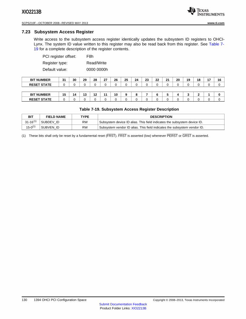
XIO2213B
SCPS210F –OCTOBER 2008–REVISED MAY 2013 www.ti.com
7.23 Subsystem Access Register
Write access to the subsystem access register identically updates the subsystem ID registers to OHCI-Lynx. The system ID value written to this register may also be read back from this register. See Table 7-19 for a complete description of the register contents.
PCI register offset: F8h
Register type: Read/Write
Default value: 0000 0000h
BIT NUMBER 31 30 29 28 27 26 25 24 23 22 21 20 19 18 17 16
RESET STATE 0 0 0 0 0 0 0 0 0 0 0 0 0 0 0 0
BIT NUMBER 15 14 13 12 11 10 9 8 7 6 5 4 3 2 1 0
RESET STATE 0 0 0 0 0 0 0 0 0 0 0 0 0 0 0 0
Table 7-19. Subsystem Access Register Description
BIT FIELD NAME TYPE DESCRIPTION
31-16 (1) SUBDEV_ID RW Subsystem device ID alias. This field indicates the subsystem device ID.
15-0(1) SUBVEN_ID RW Subsystem vendor ID alias. This field indicates the subsystem vendor ID.
(1) These bits shall only be reset by a fundamental reset (FRST). FRST is asserted (low) whenever PERST or GRST is asserted.
130 1394 OHCI PCI Configuration Space Copyright © 2008–2013, Texas Instruments Incorporated
Submit Documentation FeedbackProduct Folder Links: XIO2213B
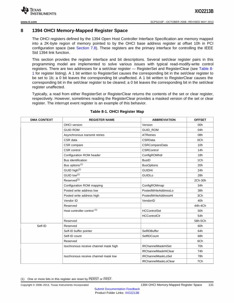
XIO2213B
www.ti.com SCPS210F –OCTOBER 2008–REVISED MAY 2013
8 1394 OHCI Memory-Mapped Register Space
The OHCI registers defined by the 1394 Open Host Controller Interface Specification are memory mappedinto a 2K-byte region of memory pointed to by the OHCI base address register at offset 10h in PCIconfiguration space (see Section 7.8). These registers are the primary interface for controlling the IEEEStd 1394 link function.
This section provides the register interface and bit descriptions. Several set/clear register pairs in thisprogramming model are implemented to solve various issues with typical read-modify-write controlregisters. There are two addresses for a set/clear register — RegisterSet and RegisterClear (see Table 8-1 for register listing). A 1 bit written to RegisterSet causes the corresponding bit in the set/clear register tobe set to 1b; a 0 bit leaves the corresponding bit unaffected. A 1 bit written to RegisterClear causes thecorresponding bit in the set/clear register to be cleared; a 0 bit leaves the corresponding bit in the set/clearregister unaffected.
Typically, a read from either RegisterSet or RegisterClear returns the contents of the set or clear register,respectively. However, sometimes reading the RegisterClear provides a masked version of the set or clearregister. The interrupt event register is an example of this behavior.
Table 8-1. OHCI Register Map
DMA CONTEXT REGISTER NAME ABBREVIATION OFFSET
OHCI version Version 00h
GUID ROM GUID_ROM 04h
Asynchronous transmit retries ATRetries 08h
CSR data CSRData 0Ch
CSR compare CSRCompareData 10h
CSR control CSRControl 14h
Configuration ROM header ConfigROMhdr 18h
Bus identification BusID 1Ch
Bus options (1) BusOptions 20h
GUID high(1) GUIDHi 24h
GUID low(1) GUIDLo 28h
Reserved(1) 2Ch-30h
Configuration ROM mapping ConfigROMmap 34h
Posted write address low PostedWriteAddressLo 38h
Posted write address high PostedWriteAddressHi 3Ch
Vendor ID VendorID 40h
Reserved 44h-4Ch
Host controller control (1) HCControlSet 50h
HCControlClr 54h
Reserved 58h-5Ch
Self-ID Reserved 60h
Self-ID buffer pointer SelfIDBuffer 64h
Self-ID count SelfIDCount 68h
Reserved 6Ch
Isochronous receive channel mask high IRChannelMaskHiSet 70h
IRChannelMaskHiClear 74h
Isochronous receive channel mask low IRChannelMaskLoSet 78h
IRChannelMaskLoClear 7Ch
(1) One or more bits in this register are reset by PERST or FRST.
Copyright © 2008–2013, Texas Instruments Incorporated 1394 OHCI Memory-Mapped Register Space 131Submit Documentation FeedbackProduct Folder Links: XIO2213B
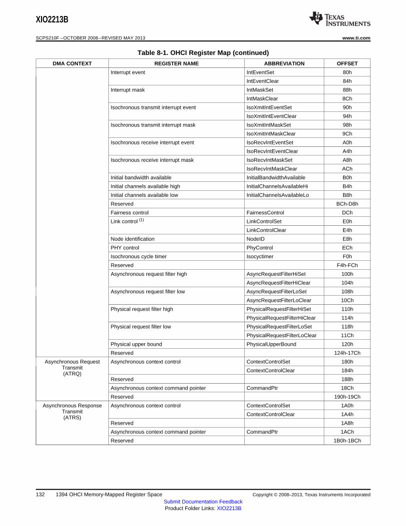
XIO2213B
SCPS210F –OCTOBER 2008–REVISED MAY 2013 www.ti.com
Table 8-1. OHCI Register Map (continued)
DMA CONTEXT REGISTER NAME ABBREVIATION OFFSET
Interrupt event IntEventSet 80h
IntEventClear 84h
Interrupt mask IntMaskSet 88h
IntMaskClear 8Ch
Isochronous transmit interrupt event IsoXmitIntEventSet 90h
IsoXmitIntEventClear 94h
Isochronous transmit interrupt mask IsoXmitIntMaskSet 98h
IsoXmitIntMaskClear 9Ch
Isochronous receive interrupt event IsoRecvIntEventSet A0h
IsoRecvIntEventClear A4h
Isochronous receive interrupt mask IsoRecvIntMaskSet A8h
IsoRecvIntMaskClear ACh
Initial bandwidth available InitialBandwidthAvailable B0h
Initial channels available high InitialChannelsAvailableHi B4h
Initial channels available low InitialChannelsAvailableLo B8h
Reserved BCh-D8h
Fairness control FairnessControl DCh
Link control (1) LinkControlSet E0h
LinkControlClear E4h
Node identification NodeID E8h
PHY control PhyControl ECh
Isochronous cycle timer Isocyctimer F0h
Reserved F4h-FCh
Asynchronous request filter high AsyncRequestFilterHiSet 100h
AsyncRequestFilterHiClear 104h
Asynchronous request filter low AsyncRequestFilterLoSet 108h
AsyncRequestFilterLoClear 10Ch
Physical request filter high PhysicalRequestFilterHiSet 110h
PhysicalRequestFilterHiClear 114h
Physical request filter low PhysicalRequestFilterLoSet 118h
PhysicalRequestFilterLoClear 11Ch
Physical upper bound PhysicalUpperBound 120h
Reserved 124h-17Ch
Asynchronous Request Asynchronous context control ContextControlSet 180hTransmit ContextControlClear 184h(ATRQ)
Reserved 188h
Asynchronous context command pointer CommandPtr 18Ch
Reserved 190h-19Ch
Asynchronous Response Asynchronous context control ContextControlSet 1A0hTransmit ContextControlClear 1A4h(ATRS)
Reserved 1A8h
Asynchronous context command pointer CommandPtr 1ACh
Reserved 1B0h-1BCh
132 1394 OHCI Memory-Mapped Register Space Copyright © 2008–2013, Texas Instruments Incorporated
Submit Documentation FeedbackProduct Folder Links: XIO2213B
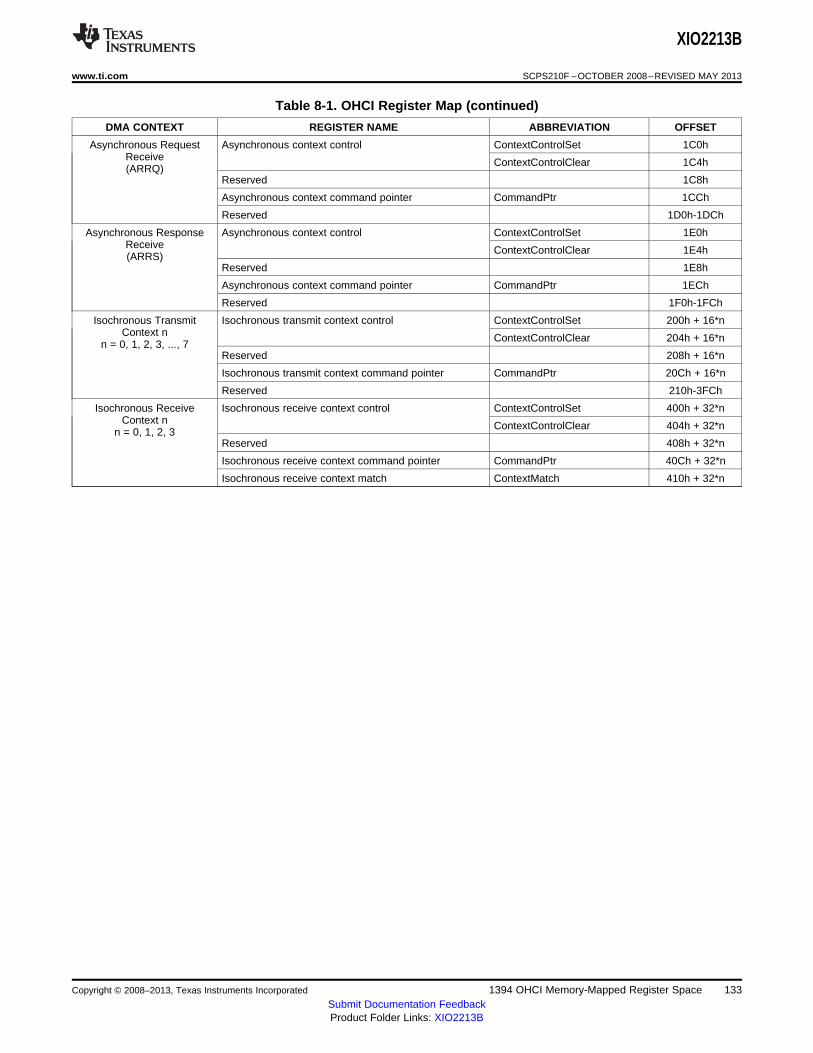
XIO2213B
www.ti.com SCPS210F –OCTOBER 2008–REVISED MAY 2013
Table 8-1. OHCI Register Map (continued)
DMA CONTEXT REGISTER NAME ABBREVIATION OFFSET
Asynchronous Request Asynchronous context control ContextControlSet 1C0hReceive ContextControlClear 1C4h(ARRQ)
Reserved 1C8h
Asynchronous context command pointer CommandPtr 1CCh
Reserved 1D0h-1DCh
Asynchronous Response Asynchronous context control ContextControlSet 1E0hReceive ContextControlClear 1E4h(ARRS)
Reserved 1E8h
Asynchronous context command pointer CommandPtr 1ECh
Reserved 1F0h-1FCh
Isochronous Transmit Isochronous transmit context control ContextControlSet 200h + 16*nContext n ContextControlClear 204h + 16*n
n = 0, 1, 2, 3, ..., 7Reserved 208h + 16*n
Isochronous transmit context command pointer CommandPtr 20Ch + 16*n
Reserved 210h-3FCh
Isochronous Receive Isochronous receive context control ContextControlSet 400h + 32*nContext n ContextControlClear 404h + 32*n
n = 0, 1, 2, 3Reserved 408h + 32*n
Isochronous receive context command pointer CommandPtr 40Ch + 32*n
Isochronous receive context match ContextMatch 410h + 32*n
Copyright © 2008–2013, Texas Instruments Incorporated 1394 OHCI Memory-Mapped Register Space 133Submit Documentation FeedbackProduct Folder Links: XIO2213B
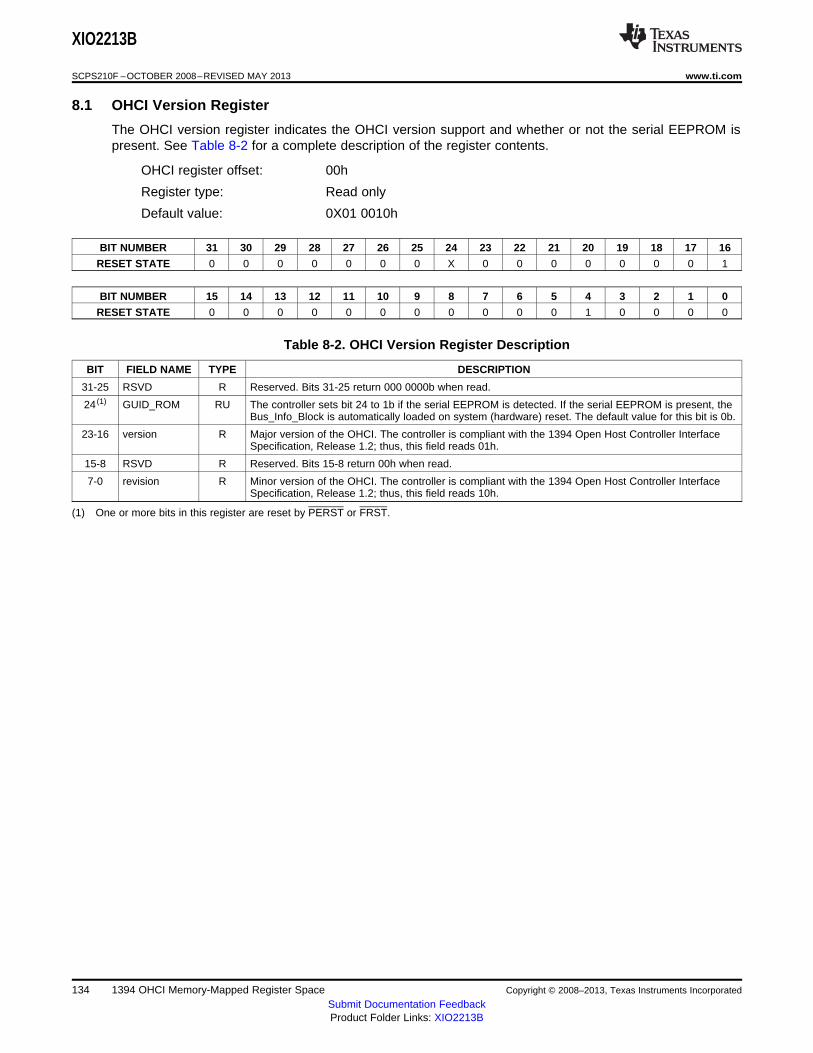
XIO2213B
SCPS210F –OCTOBER 2008–REVISED MAY 2013 www.ti.com
8.1 OHCI Version Register
The OHCI version register indicates the OHCI version support and whether or not the serial EEPROM ispresent. See Table 8-2 for a complete description of the register contents.
OHCI register offset: 00h
Register type: Read only
Default value: 0X01 0010h
BIT NUMBER 31 30 29 28 27 26 25 24 23 22 21 20 19 18 17 16
RESET STATE 0 0 0 0 0 0 0 X 0 0 0 0 0 0 0 1
BIT NUMBER 15 14 13 12 11 10 9 8 7 6 5 4 3 2 1 0
RESET STATE 0 0 0 0 0 0 0 0 0 0 0 1 0 0 0 0
Table 8-2. OHCI Version Register Description
BIT FIELD NAME TYPE DESCRIPTION
31-25 RSVD R Reserved. Bits 31-25 return 000 0000b when read.
24 (1) GUID_ROM RU The controller sets bit 24 to 1b if the serial EEPROM is detected. If the serial EEPROM is present, theBus_Info_Block is automatically loaded on system (hardware) reset. The default value for this bit is 0b.
23-16 version R Major version of the OHCI. The controller is compliant with the 1394 Open Host Controller InterfaceSpecification, Release 1.2; thus, this field reads 01h.
15-8 RSVD R Reserved. Bits 15-8 return 00h when read.
7-0 revision R Minor version of the OHCI. The controller is compliant with the 1394 Open Host Controller InterfaceSpecification, Release 1.2; thus, this field reads 10h.
(1) One or more bits in this register are reset by PERST or FRST.
134 1394 OHCI Memory-Mapped Register Space Copyright © 2008–2013, Texas Instruments Incorporated
Submit Documentation FeedbackProduct Folder Links: XIO2213B
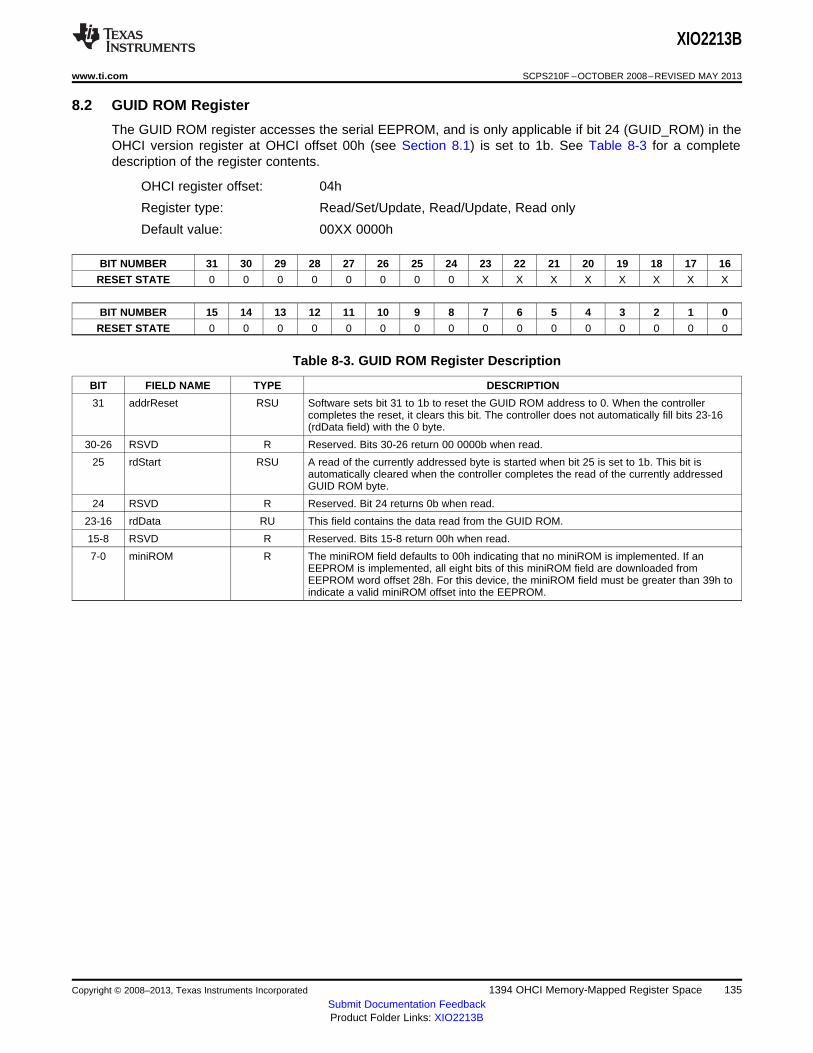
XIO2213B
www.ti.com SCPS210F –OCTOBER 2008–REVISED MAY 2013
8.2 GUID ROM Register
The GUID ROM register accesses the serial EEPROM, and is only applicable if bit 24 (GUID_ROM) in theOHCI version register at OHCI offset 00h (see Section 8.1) is set to 1b. See Table 8-3 for a completedescription of the register contents.
OHCI register offset: 04h
Register type: Read/Set/Update, Read/Update, Read only
Default value: 00XX 0000h
BIT NUMBER 31 30 29 28 27 26 25 24 23 22 21 20 19 18 17 16
RESET STATE 0 0 0 0 0 0 0 0 X X X X X X X X
BIT NUMBER 15 14 13 12 11 10 9 8 7 6 5 4 3 2 1 0
RESET STATE 0 0 0 0 0 0 0 0 0 0 0 0 0 0 0 0
Table 8-3. GUID ROM Register Description
BIT FIELD NAME TYPE DESCRIPTION
31 addrReset RSU Software sets bit 31 to 1b to reset the GUID ROM address to 0. When the controllercompletes the reset, it clears this bit. The controller does not automatically fill bits 23-16(rdData field) with the 0 byte.
30-26 RSVD R Reserved. Bits 30-26 return 00 0000b when read.
25 rdStart RSU A read of the currently addressed byte is started when bit 25 is set to 1b. This bit isautomatically cleared when the controller completes the read of the currently addressedGUID ROM byte.
24 RSVD R Reserved. Bit 24 returns 0b when read.
23-16 rdData RU This field contains the data read from the GUID ROM.
15-8 RSVD R Reserved. Bits 15-8 return 00h when read.
7-0 miniROM R The miniROM field defaults to 00h indicating that no miniROM is implemented. If anEEPROM is implemented, all eight bits of this miniROM field are downloaded fromEEPROM word offset 28h. For this device, the miniROM field must be greater than 39h toindicate a valid miniROM offset into the EEPROM.
Copyright © 2008–2013, Texas Instruments Incorporated 1394 OHCI Memory-Mapped Register Space 135Submit Documentation FeedbackProduct Folder Links: XIO2213B
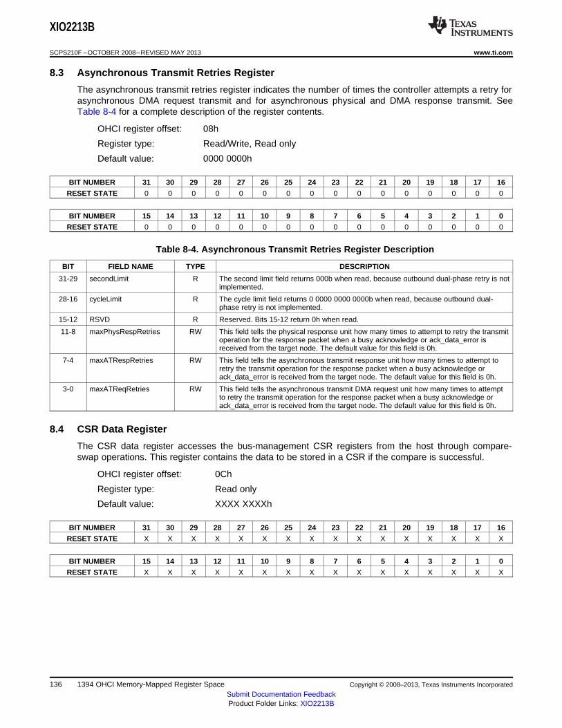
XIO2213B
SCPS210F –OCTOBER 2008–REVISED MAY 2013 www.ti.com
8.3 Asynchronous Transmit Retries Register
The asynchronous transmit retries register indicates the number of times the controller attempts a retry forasynchronous DMA request transmit and for asynchronous physical and DMA response transmit. SeeTable 8-4 for a complete description of the register contents.
OHCI register offset: 08h
Register type: Read/Write, Read only
Default value: 0000 0000h
BIT NUMBER 31 30 29 28 27 26 25 24 23 22 21 20 19 18 17 16
RESET STATE 0 0 0 0 0 0 0 0 0 0 0 0 0 0 0 0
BIT NUMBER 15 14 13 12 11 10 9 8 7 6 5 4 3 2 1 0
RESET STATE 0 0 0 0 0 0 0 0 0 0 0 0 0 0 0 0
Table 8-4. Asynchronous Transmit Retries Register Description
BIT FIELD NAME TYPE DESCRIPTION
31-29 secondLimit R The second limit field returns 000b when read, because outbound dual-phase retry is notimplemented.
28-16 cycleLimit R The cycle limit field returns 0 0000 0000 0000b when read, because outbound dual-phase retry is not implemented.
15-12 RSVD R Reserved. Bits 15-12 return 0h when read.
11-8 maxPhysRespRetries RW This field tells the physical response unit how many times to attempt to retry the transmitoperation for the response packet when a busy acknowledge or ack_data_error isreceived from the target node. The default value for this field is 0h.
7-4 maxATRespRetries RW This field tells the asynchronous transmit response unit how many times to attempt toretry the transmit operation for the response packet when a busy acknowledge orack_data_error is received from the target node. The default value for this field is 0h.
3-0 maxATReqRetries RW This field tells the asynchronous transmit DMA request unit how many times to attemptto retry the transmit operation for the response packet when a busy acknowledge orack_data_error is received from the target node. The default value for this field is 0h.
8.4 CSR Data Register
The CSR data register accesses the bus-management CSR registers from the host through compare-swap operations. This register contains the data to be stored in a CSR if the compare is successful.
OHCI register offset: 0Ch
Register type: Read only
Default value: XXXX XXXXh
BIT NUMBER 31 30 29 28 27 26 25 24 23 22 21 20 19 18 17 16
RESET STATE X X X X X X X X X X X X X X X X
BIT NUMBER 15 14 13 12 11 10 9 8 7 6 5 4 3 2 1 0
RESET STATE X X X X X X X X X X X X X X X X
136 1394 OHCI Memory-Mapped Register Space Copyright © 2008–2013, Texas Instruments Incorporated
Submit Documentation FeedbackProduct Folder Links: XIO2213B
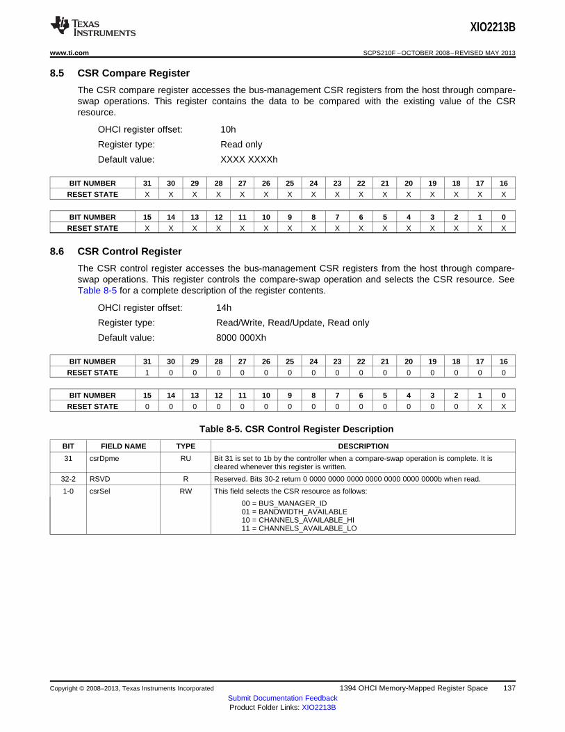
XIO2213B
www.ti.com SCPS210F –OCTOBER 2008–REVISED MAY 2013
8.5 CSR Compare Register
The CSR compare register accesses the bus-management CSR registers from the host through compare-swap operations. This register contains the data to be compared with the existing value of the CSRresource.
OHCI register offset: 10h
Register type: Read only
Default value: XXXX XXXXh
BIT NUMBER 31 30 29 28 27 26 25 24 23 22 21 20 19 18 17 16
RESET STATE X X X X X X X X X X X X X X X X
BIT NUMBER 15 14 13 12 11 10 9 8 7 6 5 4 3 2 1 0
RESET STATE X X X X X X X X X X X X X X X X
8.6 CSR Control Register
The CSR control register accesses the bus-management CSR registers from the host through compare-swap operations. This register controls the compare-swap operation and selects the CSR resource. SeeTable 8-5 for a complete description of the register contents.
OHCI register offset: 14h
Register type: Read/Write, Read/Update, Read only
Default value: 8000 000Xh
BIT NUMBER 31 30 29 28 27 26 25 24 23 22 21 20 19 18 17 16
RESET STATE 1 0 0 0 0 0 0 0 0 0 0 0 0 0 0 0
BIT NUMBER 15 14 13 12 11 10 9 8 7 6 5 4 3 2 1 0
RESET STATE 0 0 0 0 0 0 0 0 0 0 0 0 0 0 X X
Table 8-5. CSR Control Register Description
BIT FIELD NAME TYPE DESCRIPTION
31 csrDpme RU Bit 31 is set to 1b by the controller when a compare-swap operation is complete. It iscleared whenever this register is written.
32-2 RSVD R Reserved. Bits 30-2 return 0 0000 0000 0000 0000 0000 0000 0000b when read.
1-0 csrSel RW This field selects the CSR resource as follows:
00 = BUS_MANAGER_ID01 = BANDWIDTH_AVAILABLE10 = CHANNELS_AVAILABLE_HI11 = CHANNELS_AVAILABLE_LO
Copyright © 2008–2013, Texas Instruments Incorporated 1394 OHCI Memory-Mapped Register Space 137Submit Documentation FeedbackProduct Folder Links: XIO2213B
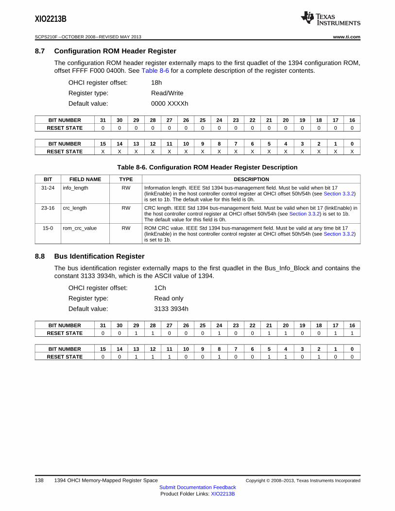
XIO2213B
SCPS210F –OCTOBER 2008–REVISED MAY 2013 www.ti.com
8.7 Configuration ROM Header Register
The configuration ROM header register externally maps to the first quadlet of the 1394 configuration ROM,offset FFFF F000 0400h. See Table 8-6 for a complete description of the register contents.
OHCI register offset: 18h
Register type: Read/Write
Default value: 0000 XXXXh
BIT NUMBER 31 30 29 28 27 26 25 24 23 22 21 20 19 18 17 16
RESET STATE 0 0 0 0 0 0 0 0 0 0 0 0 0 0 0 0
BIT NUMBER 15 14 13 12 11 10 9 8 7 6 5 4 3 2 1 0
RESET STATE X X X X X X X X X X X X X X X X
Table 8-6. Configuration ROM Header Register Description
BIT FIELD NAME TYPE DESCRIPTION
31-24 info_length RW Information length. IEEE Std 1394 bus-management field. Must be valid when bit 17(linkEnable) in the host controller control register at OHCI offset 50h/54h (see Section 3.3.2)is set to 1b. The default value for this field is 0h.
23-16 crc_length RW CRC length. IEEE Std 1394 bus-management field. Must be valid when bit 17 (linkEnable) inthe host controller control register at OHCI offset 50h/54h (see Section 3.3.2) is set to 1b.The default value for this field is 0h.
15-0 rom_crc_value RW ROM CRC value. IEEE Std 1394 bus-management field. Must be valid at any time bit 17(linkEnable) in the host controller control register at OHCI offset 50h/54h (see Section 3.3.2)is set to 1b.
8.8 Bus Identification Register
The bus identification register externally maps to the first quadlet in the Bus_Info_Block and contains theconstant 3133 3934h, which is the ASCII value of 1394.
OHCI register offset: 1Ch
Register type: Read only
Default value: 3133 3934h
BIT NUMBER 31 30 29 28 27 26 25 24 23 22 21 20 19 18 17 16
RESET STATE 0 0 1 1 0 0 0 1 0 0 1 1 0 0 1 1
BIT NUMBER 15 14 13 12 11 10 9 8 7 6 5 4 3 2 1 0
RESET STATE 0 0 1 1 1 0 0 1 0 0 1 1 0 1 0 0
138 1394 OHCI Memory-Mapped Register Space Copyright © 2008–2013, Texas Instruments Incorporated
Submit Documentation FeedbackProduct Folder Links: XIO2213B
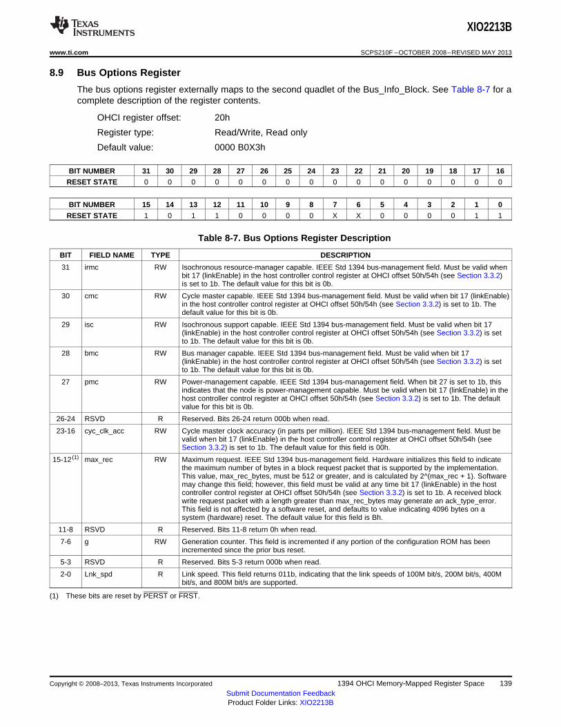
XIO2213B
www.ti.com SCPS210F –OCTOBER 2008–REVISED MAY 2013
8.9 Bus Options Register
The bus options register externally maps to the second quadlet of the Bus_Info_Block. See Table 8-7 for acomplete description of the register contents.
OHCI register offset: 20h
Register type: Read/Write, Read only
Default value: 0000 B0X3h
BIT NUMBER 31 30 29 28 27 26 25 24 23 22 21 20 19 18 17 16
RESET STATE 0 0 0 0 0 0 0 0 0 0 0 0 0 0 0 0
BIT NUMBER 15 14 13 12 11 10 9 8 7 6 5 4 3 2 1 0
RESET STATE 1 0 1 1 0 0 0 0 X X 0 0 0 0 1 1
Table 8-7. Bus Options Register Description
BIT FIELD NAME TYPE DESCRIPTION
31 irmc RW Isochronous resource-manager capable. IEEE Std 1394 bus-management field. Must be valid whenbit 17 (linkEnable) in the host controller control register at OHCI offset 50h/54h (see Section 3.3.2)is set to 1b. The default value for this bit is 0b.
30 cmc RW Cycle master capable. IEEE Std 1394 bus-management field. Must be valid when bit 17 (linkEnable)in the host controller control register at OHCI offset 50h/54h (see Section 3.3.2) is set to 1b. Thedefault value for this bit is 0b.
29 isc RW Isochronous support capable. IEEE Std 1394 bus-management field. Must be valid when bit 17(linkEnable) in the host controller control register at OHCI offset 50h/54h (see Section 3.3.2) is setto 1b. The default value for this bit is 0b.
28 bmc RW Bus manager capable. IEEE Std 1394 bus-management field. Must be valid when bit 17(linkEnable) in the host controller control register at OHCI offset 50h/54h (see Section 3.3.2) is setto 1b. The default value for this bit is 0b.
27 pmc RW Power-management capable. IEEE Std 1394 bus-management field. When bit 27 is set to 1b, thisindicates that the node is power-management capable. Must be valid when bit 17 (linkEnable) in thehost controller control register at OHCI offset 50h/54h (see Section 3.3.2) is set to 1b. The defaultvalue for this bit is 0b.
26-24 RSVD R Reserved. Bits 26-24 return 000b when read.
23-16 cyc_clk_acc RW Cycle master clock accuracy (in parts per million). IEEE Std 1394 bus-management field. Must bevalid when bit 17 (linkEnable) in the host controller control register at OHCI offset 50h/54h (seeSection 3.3.2) is set to 1b. The default value for this field is 00h.
15-12 (1) max_rec RW Maximum request. IEEE Std 1394 bus-management field. Hardware initializes this field to indicatethe maximum number of bytes in a block request packet that is supported by the implementation.This value, max_rec_bytes, must be 512 or greater, and is calculated by 2^(max_rec + 1). Softwaremay change this field; however, this field must be valid at any time bit 17 (linkEnable) in the hostcontroller control register at OHCI offset 50h/54h (see Section 3.3.2) is set to 1b. A received blockwrite request packet with a length greater than max_rec_bytes may generate an ack_type_error.This field is not affected by a software reset, and defaults to value indicating 4096 bytes on asystem (hardware) reset. The default value for this field is Bh.
11-8 RSVD R Reserved. Bits 11-8 return 0h when read.
7-6 g RW Generation counter. This field is incremented if any portion of the configuration ROM has beenincremented since the prior bus reset.
5-3 RSVD R Reserved. Bits 5-3 return 000b when read.
2-0 Lnk_spd R Link speed. This field returns 011b, indicating that the link speeds of 100M bit/s, 200M bit/s, 400Mbit/s, and 800M bit/s are supported.
(1) These bits are reset by PERST or FRST.
Copyright © 2008–2013, Texas Instruments Incorporated 1394 OHCI Memory-Mapped Register Space 139Submit Documentation FeedbackProduct Folder Links: XIO2213B
XIO2213B
SCPS210F –OCTOBER 2008–REVISED MAY 2013 www.ti.com
8.10 GUID High Register
The GUID high register represents the upper quadlet in a 64-bit global unique ID (GUID), which maps tothe third quadlet in the Bus_Info_Block. This register contains node_vendor_ID and chip_ID_hi fields. Thisregister initializes to 0000 0000h on a system (hardware) reset, which is an illegal GUID value. If a serialEEPROM is detected, the contents of this register are loaded through the serial EEPROM interface. Atthat point, the contents of this register cannot be changed. If no serial EEPROM is detected, the contentsof this register are loaded by the BIOS. At that point, the contents of this register cannot be changed. Thisregister is reset by a PCIe reset (PERST), GRST, or the internally-generated power-on reset.
OHCI register offset: 24h
Register type: Read only
Default value: 0000 0000h
BIT NUMBER 31 30 29 28 27 26 25 24 23 22 21 20 19 18 17 16
RESET STATE 0 0 0 0 0 0 0 0 0 0 0 0 0 0 0 0
BIT NUMBER 15 14 13 12 11 10 9 8 7 6 5 4 3 (1) 2 (1) 1 (1) 0 (1)
RESET STATE 0 0 0 0 0 0 0 0 0 0 0 0 0 0 0 0
(1) These bits are reset only by a global reset (GRST) or the internally generated power-on reset.
8.11 GUID Low Register
The GUID low register represents the lower quadlet in a 64-bit global unique ID (GUID), which maps tochip_ID_lo in the Bus_Info_Block. This register initializes to 0000 0000h on a system (hardware) reset andbehaves identical to the GUID high register at OHCI offset 24h (see Section 8.10). This register is reset byPERST, GRST, or the internally-generated power-on reset.
OHCI register offset: 28h
Register type: Read only
Default value: 0000 0000h
BIT NUMBER 31 30 29 28 27 26 25 24 23 22 21 20 19 18 17 16
RESET STATE 0 0 0 0 0 0 0 0 0 0 0 0 0 0 0 0
BIT NUMBER 15 14 13 12 11 10 9 8 7 6 5 4 3 (1) 2 (1) 1 (1) 0 (1)
RESET STATE 0 0 0 0 0 0 0 0 0 0 0 0 0 0 0 0
(1) These bits are reset only by a global reset (GRST) or the internally generated power-on reset.
140 1394 OHCI Memory-Mapped Register Space Copyright © 2008–2013, Texas Instruments Incorporated
Submit Documentation FeedbackProduct Folder Links: XIO2213B
XIO2213B
www.ti.com SCPS210F –OCTOBER 2008–REVISED MAY 2013
8.12 Configuration ROM Mapping Register
The configuration ROM mapping register contains the start address within system memory that maps tothe start address of 1394 configuration ROM for this node. See Table 8-8 for a complete description of theregister contents.
OHCI register offset:: 34h
Register type: Read/Write
Default value: 0000 0000h
BIT NUMBER 31 30 29 28 27 26 25 24 23 22 21 20 19 18 17 16
RESET STATE 0 0 0 0 0 0 0 0 0 0 0 0 0 0 0 0
BIT NUMBER 15 14 13 12 11 10 9 8 7 6 5 4 3 2 1 0
RESET STATE 0 0 0 0 0 0 0 0 0 0 0 0 0 0 0 0
Table 8-8. Configuration ROM Mapping Register Description
BIT FIELD NAME TYPE DESCRIPTION
31-10 configROMaddr RW Configuration ROM address. If a quadlet read request to 1394 offset FFFF F000 0400h throughoffset FFFF F000 07FFh is received, the low-order ten bits of the offset are added to this register todetermine the host memory address of the read request. The default value for this field is all 0s.
9-0 RSVD R Reserved. Bits 9-0 return 00 0000 0000b when read.
8.13 Posted Write Address Low Register
The posted write address low register communicates error information if a write request is posted and anerror occurs while the posted data packet is being written. See Table 8-9 for a complete description of theregister contents.
OHCI register offset: 38h
Register type: Read/Update
Default value: XXXX XXXXh
BIT NUMBER 31 30 29 28 27 26 25 24 23 22 21 20 19 18 17 16
RESET STATE X X X X X X X X X X X X X X X X
BIT NUMBER 15 14 13 12 11 10 9 8 7 6 5 4 3 2 1 0
RESET STATE X X X X X X X X X X X X X X X X
Table 8-9. Posted Write Address Low Register Description
BIT FIELD NAME TYPE DESCRIPTION
31-0 offsetLo RU Offset low. The lower 32 bits of the 1394 destination offset of the write request that failed.
Copyright © 2008–2013, Texas Instruments Incorporated 1394 OHCI Memory-Mapped Register Space 141Submit Documentation FeedbackProduct Folder Links: XIO2213B
XIO2213B
SCPS210F –OCTOBER 2008–REVISED MAY 2013 www.ti.com
8.14 Posted Write Address High Register
The posted write address high register communicates error information if a write request is posted and anerror occurs while writing the posted data packet. See Table 8-10 for a complete description of the registercontents.
OHCI register offset: 3Ch
Register type: Read/Update
Default value: XXXX XXXXh
BIT NUMBER 31 30 29 28 27 26 25 24 23 22 21 20 19 18 17 16
RESET STATE X X X X X X X X X X X X X X X X
BIT NUMBER 15 14 13 12 11 10 9 8 7 6 5 4 3 2 1 0
RESET STATE X X X X X X X X X X X X X X X X
Table 8-10. Posted Write Address High Register Description
BIT FIELD NAME TYPE DESCRIPTION
31-16 sourceID RU Source identification. This field is the 10-bit bus number (bits 31-22) and 6-bit node number(bits 21-16) of the node that issued the write request that failed.
15-0 offsetHi RU Offset high. The upper 16 bits of the 1394 destination offset of the write request that failed.
8.15 Vendor ID Register
The vendor ID register holds the company ID of an organization that specifies any vendor-uniqueregisters. The controller implements TI unique behavior with regards to OHCI. Thus, this register is readonly and returns 0x08 0028h when read.
OHCI register offset: 40h
Register type: Read only
Default value: 0x08 0028h
BIT NUMBER 31 30 29 28 27 26 25 24 23 22 21 20 19 18 17 16
RESET STATE 0 0 0 0 0 x x 1 0 0 0 0 1 0 0 0
BIT NUMBER 15 14 13 12 11 10 9 8 7 6 5 4 3 2 1 0
RESET STATE 0 0 0 0 0 0 0 0 0 0 1 0 1 0 0 0
8.16 Host Controller Control Register
The host controller control set/clear register pair provides flags for controlling the controller. See Table 8-11 for a complete description of the register contents.
OHCI register offset: 50h set register54h clear register
Register type: Read/Set/Clear/Update, Read/Set/Clear, Read/Clear, Read only
Default value: 0080 0000h
BIT NUMBER 31 30 29 28 27 26 25 24 23 22 21 20 19 18 17 16
RESET STATE 0 0 0 0 0 0 0 0 1 0 0 0 0 0 0 0
142 1394 OHCI Memory-Mapped Register Space Copyright © 2008–2013, Texas Instruments Incorporated
Submit Documentation FeedbackProduct Folder Links: XIO2213B

XIO2213B
www.ti.com SCPS210F –OCTOBER 2008–REVISED MAY 2013
BIT NUMBER 15 14 13 12 11 10 9 8 7 6 5 4 3 2 1 0
RESET STATE 0 0 0 0 0 0 0 0 0 0 0 0 0 0 0 0
Copyright © 2008–2013, Texas Instruments Incorporated 1394 OHCI Memory-Mapped Register Space 143Submit Documentation FeedbackProduct Folder Links: XIO2213B
XIO2213B
SCPS210F –OCTOBER 2008–REVISED MAY 2013 www.ti.com
Table 8-11. Host Controller Control Register Description
BIT FIELD NAME TYPE DESCRIPTION
31 BIBimageValid RSU When bit 31 is set to 1b, the physical response unit is enabled to respond to block read requeststo host configuration ROM and to the mechanism for atomically updating configuration ROM.Software creates a valid image of the bus_info_block in host configuration ROM before setting thisbit.
When this bit is cleared, the controller returns ack_type_error on block read requests to hostconfiguration ROM. Also, when this bit is cleared and a 1394 bus reset occurs, the configurationROM mapping register at OHCI offset 34h (see Section 8.12), configuration ROM header registerat OHCI offset 18h (see Section 8.7), and bus options register at OHCI offset 20h (seeSection 8.9) are not updated.
Software can set this bit only when bit 17 (linkEnable) is 0b. Once bit 31 is set to 1b, it can becleared by a system (hardware) reset, a software reset, or if a fetch error occurs when thecontroller loads bus_info_block registers from host memory.
30 noByteSwapData RSC Bit 30 controls whether physical accesses to locations outside the controller itself, as well as anyother DMA data accesses are byte swapped.
29 ack_Tardy_enable RSC Bit 29 controls the acknowledgement of ack_tardy. When bit 29 is set to 1b, ack_tardy may bereturned as an acknowledgment to accesses from the 1394 bus to the controller, includingaccesses to the bus_info_block. The controller returns ack_tardy to all other asynchronouspackets addressed to the node. When the controller sends ack_tardy, bit 27 (ack_tardy) in theinterrupt event register at OHCI offset 80h/84h (see Section 8.21) is set to 1b to indicate theattempted asynchronous access.
Software ensures that bit 27 (ack_tardy) in the interrupt event register is 0b. Software alsounmasks wake-up interrupt events such as bit 19 (phy) and bit 27 (ack_tardy) in the interruptevent register before placing the controller into the D1 power mode.
Software must not set this bit if the node is the 1394 bus manager.
28-24 RSVD R Reserved. Bits 28-24 return 00000b when read.
23 (1) programPhyEnable RC Bit 23 informs upper-level software that lower-level software has consistently configured the IEEEStd 1394a-2000 enhancements in the link and PHYs. When this bit is 1b, generic software suchas the OHCI driver is responsible for configuring IEEE Std 1394a-2000 enhancements in the PHYand bit 22 (aPhyEnhanceEnable). When this bit is 0b, the generic software may not modify theIEEE Std 1394a-2000 enhancements in the PHY and cannot interpret the setting of bit 22(aPhyEnhanceEnable). This bit is initialized from serial EEPROM.
22 aPhyEnhanceEnabl RSC When bits 23 (programPhyEnable) and 17 (linkEnable) are 11b, the OHCI driver can set bit 22 toe 1b to use all IEEE Std 1394a-2000 enhancements. When bit 23 (programPhyEnable) is cleared to
0b, the software does not change PHY enhancements or this bit.
21-20 RSVD R Reserved. Bits 21 and 20 return 00b when read.
19 LPS RSC Bit 19 controls the link power status. Software must set this bit to 1b to permit the link-PHYcommunication. A 0b prevents link-PHY communication.
The OHCI link is divided into two clock domains (PCLK and PHY_SCLK). If software tries toaccess any register in the PHY_SCLK domain while the PHY_SCLK is disabled, a target abort isissued by the link. This problem can be avoided by setting bit 4 (DIS_TGT_ABT) to 1b in the PCImiscellaneous configuration register at offset F0h in the PCI configuration space (seeSection 7.21). This allows the link to respond to these types of request by returning all Fs (hex).
OHCI registers at offsets DCh-F0h and 100h-11Ch are in the PHY_SCLK domain.
After setting LPS, software must wait approximately 10 ms before attempting to access any of theOHCI registers. This gives the PHY_SCLK time to stabilize.
18 postedWriteEnable RSC Bit 18 enables (1) or disables (0) posted writes. Software changes this bit only when bit 17(linkEnable) is 0b.
17 linkEnable RSC Bit 17 is cleared to 0b by either a system (hardware) or software reset. Software must set this bitto 1b when the system is ready to begin operation and then force a bus reset. This bit isnecessary to keep other nodes from sending transactions before the local system is ready. Whenthis bit is cleared, the controller is logically and immediately disconnected from the 1394 bus, nopackets are received or processed, nor are packets transmitted.
16 SoftReset RSCU When bit 16 is set to 1b, all states are reset, all FIFOs are flushed, and all OHCI registers are setto their system (hardware) reset values, unless otherwise specified. PCI registers are not affectedby this bit. This bit remains set to 1b while the software reset is in progress and reverts back to 0bwhen the reset has completed.
15-0 RSVD R Reserved. Bits 15-0 return 0000h when read.
(1) This bit is reset by PERST or FRST.
144 1394 OHCI Memory-Mapped Register Space Copyright © 2008–2013, Texas Instruments Incorporated
Submit Documentation FeedbackProduct Folder Links: XIO2213B
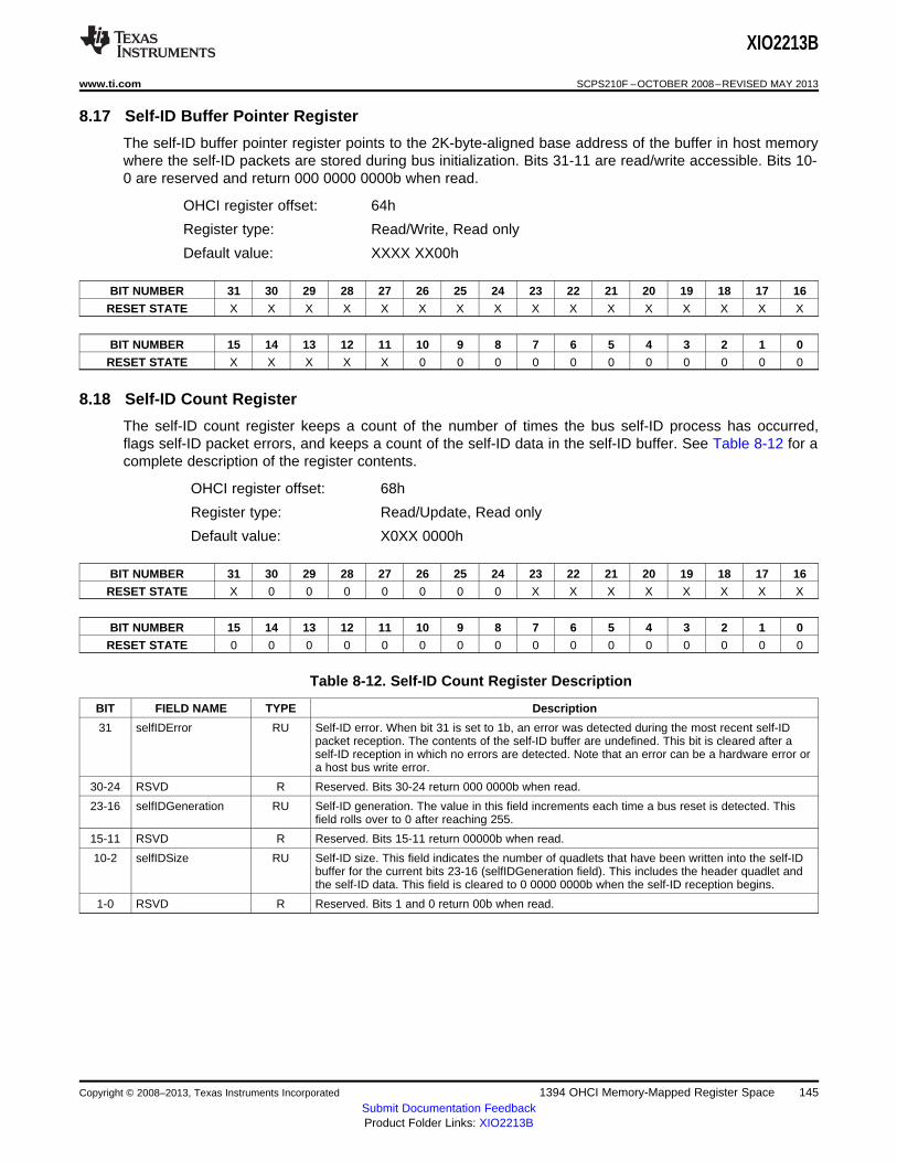
XIO2213B
www.ti.com SCPS210F –OCTOBER 2008–REVISED MAY 2013
8.17 Self-ID Buffer Pointer Register
The self-ID buffer pointer register points to the 2K-byte-aligned base address of the buffer in host memorywhere the self-ID packets are stored during bus initialization. Bits 31-11 are read/write accessible. Bits 10-0 are reserved and return 000 0000 0000b when read.
OHCI register offset: 64h
Register type: Read/Write, Read only
Default value: XXXX XX00h
BIT NUMBER 31 30 29 28 27 26 25 24 23 22 21 20 19 18 17 16
RESET STATE X X X X X X X X X X X X X X X X
BIT NUMBER 15 14 13 12 11 10 9 8 7 6 5 4 3 2 1 0
RESET STATE X X X X X 0 0 0 0 0 0 0 0 0 0 0
8.18 Self-ID Count Register
The self-ID count register keeps a count of the number of times the bus self-ID process has occurred,flags self-ID packet errors, and keeps a count of the self-ID data in the self-ID buffer. See Table 8-12 for acomplete description of the register contents.
OHCI register offset: 68h
Register type: Read/Update, Read only
Default value: X0XX 0000h
BIT NUMBER 31 30 29 28 27 26 25 24 23 22 21 20 19 18 17 16
RESET STATE X 0 0 0 0 0 0 0 X X X X X X X X
BIT NUMBER 15 14 13 12 11 10 9 8 7 6 5 4 3 2 1 0
RESET STATE 0 0 0 0 0 0 0 0 0 0 0 0 0 0 0 0
Table 8-12. Self-ID Count Register Description
BIT FIELD NAME TYPE Description
31 selfIDError RU Self-ID error. When bit 31 is set to 1b, an error was detected during the most recent self-IDpacket reception. The contents of the self-ID buffer are undefined. This bit is cleared after aself-ID reception in which no errors are detected. Note that an error can be a hardware error ora host bus write error.
30-24 RSVD R Reserved. Bits 30-24 return 000 0000b when read.
23-16 selfIDGeneration RU Self-ID generation. The value in this field increments each time a bus reset is detected. Thisfield rolls over to 0 after reaching 255.
15-11 RSVD R Reserved. Bits 15-11 return 00000b when read.
10-2 selfIDSize RU Self-ID size. This field indicates the number of quadlets that have been written into the self-IDbuffer for the current bits 23-16 (selfIDGeneration field). This includes the header quadlet andthe self-ID data. This field is cleared to 0 0000 0000b when the self-ID reception begins.
1-0 RSVD R Reserved. Bits 1 and 0 return 00b when read.
Copyright © 2008–2013, Texas Instruments Incorporated 1394 OHCI Memory-Mapped Register Space 145Submit Documentation FeedbackProduct Folder Links: XIO2213B
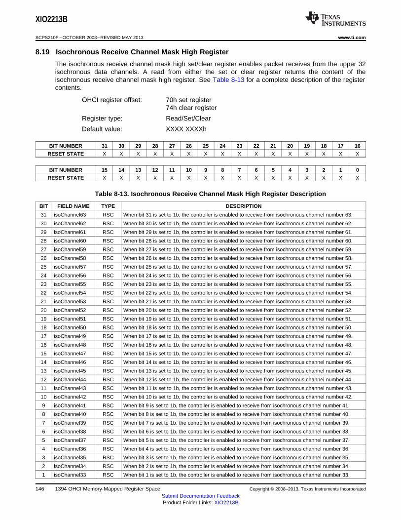
XIO2213B
SCPS210F –OCTOBER 2008–REVISED MAY 2013 www.ti.com
8.19 Isochronous Receive Channel Mask High Register
The isochronous receive channel mask high set/clear register enables packet receives from the upper 32isochronous data channels. A read from either the set or clear register returns the content of theisochronous receive channel mask high register. See Table 8-13 for a complete description of the registercontents.
OHCI register offset: 70h set register74h clear register
Register type: Read/Set/Clear
Default value: XXXX XXXXh
BIT NUMBER 31 30 29 28 27 26 25 24 23 22 21 20 19 18 17 16
RESET STATE X X X X X X X X X X X X X X X X
BIT NUMBER 15 14 13 12 11 10 9 8 7 6 5 4 3 2 1 0
RESET STATE X X X X X X X X X X X X X X X X
Table 8-13. Isochronous Receive Channel Mask High Register Description
BIT FIELD NAME TYPE DESCRIPTION
31 isoChannel63 RSC When bit 31 is set to 1b, the controller is enabled to receive from isochronous channel number 63.
30 isoChannel62 RSC When bit 30 is set to 1b, the controller is enabled to receive from isochronous channel number 62.
29 isoChannel61 RSC When bit 29 is set to 1b, the controller is enabled to receive from isochronous channel number 61.
28 isoChannel60 RSC When bit 28 is set to 1b, the controller is enabled to receive from isochronous channel number 60.
27 isoChannel59 RSC When bit 27 is set to 1b, the controller is enabled to receive from isochronous channel number 59.
26 isoChannel58 RSC When bit 26 is set to 1b, the controller is enabled to receive from isochronous channel number 58.
25 isoChannel57 RSC When bit 25 is set to 1b, the controller is enabled to receive from isochronous channel number 57.
24 isoChannel56 RSC When bit 24 is set to 1b, the controller is enabled to receive from isochronous channel number 56.
23 isoChannel55 RSC When bit 23 is set to 1b, the controller is enabled to receive from isochronous channel number 55.
22 isoChannel54 RSC When bit 22 is set to 1b, the controller is enabled to receive from isochronous channel number 54.
21 isoChannel53 RSC When bit 21 is set to 1b, the controller is enabled to receive from isochronous channel number 53.
20 isoChannel52 RSC When bit 20 is set to 1b, the controller is enabled to receive from isochronous channel number 52.
19 isoChannel51 RSC When bit 19 is set to 1b, the controller is enabled to receive from isochronous channel number 51.
18 isoChannel50 RSC When bit 18 is set to 1b, the controller is enabled to receive from isochronous channel number 50.
17 isoChannel49 RSC When bit 17 is set to 1b, the controller is enabled to receive from isochronous channel number 49.
16 isoChannel48 RSC When bit 16 is set to 1b, the controller is enabled to receive from isochronous channel number 48.
15 isoChannel47 RSC When bit 15 is set to 1b, the controller is enabled to receive from isochronous channel number 47.
14 isoChannel46 RSC When bit 14 is set to 1b, the controller is enabled to receive from isochronous channel number 46.
13 isoChannel45 RSC When bit 13 is set to 1b, the controller is enabled to receive from isochronous channel number 45.
12 isoChannel44 RSC When bit 12 is set to 1b, the controller is enabled to receive from isochronous channel number 44.
11 isoChannel43 RSC When bit 11 is set to 1b, the controller is enabled to receive from isochronous channel number 43.
10 isoChannel42 RSC When bit 10 is set to 1b, the controller is enabled to receive from isochronous channel number 42.
9 isoChannel41 RSC When bit 9 is set to 1b, the controller is enabled to receive from isochronous channel number 41.
8 isoChannel40 RSC When bit 8 is set to 1b, the controller is enabled to receive from isochronous channel number 40.
7 isoChannel39 RSC When bit 7 is set to 1b, the controller is enabled to receive from isochronous channel number 39.
6 isoChannel38 RSC When bit 6 is set to 1b, the controller is enabled to receive from isochronous channel number 38.
5 isoChannel37 RSC When bit 5 is set to 1b, the controller is enabled to receive from isochronous channel number 37.
4 isoChannel36 RSC When bit 4 is set to 1b, the controller is enabled to receive from isochronous channel number 36.
3 isoChannel35 RSC When bit 3 is set to 1b, the controller is enabled to receive from isochronous channel number 35.
2 isoChannel34 RSC When bit 2 is set to 1b, the controller is enabled to receive from isochronous channel number 34.
1 isoChannel33 RSC When bit 1 is set to 1b, the controller is enabled to receive from isochronous channel number 33.
146 1394 OHCI Memory-Mapped Register Space Copyright © 2008–2013, Texas Instruments Incorporated
Submit Documentation FeedbackProduct Folder Links: XIO2213B

XIO2213B
www.ti.com SCPS210F –OCTOBER 2008–REVISED MAY 2013
Table 8-13. Isochronous Receive Channel Mask High Register Description (continued)
BIT FIELD NAME TYPE DESCRIPTION
0 isoChannel32 RSC When bit 0 is set to 1b, the controller is enabled to receive from isochronous channel number 32.
Copyright © 2008–2013, Texas Instruments Incorporated 1394 OHCI Memory-Mapped Register Space 147Submit Documentation FeedbackProduct Folder Links: XIO2213B
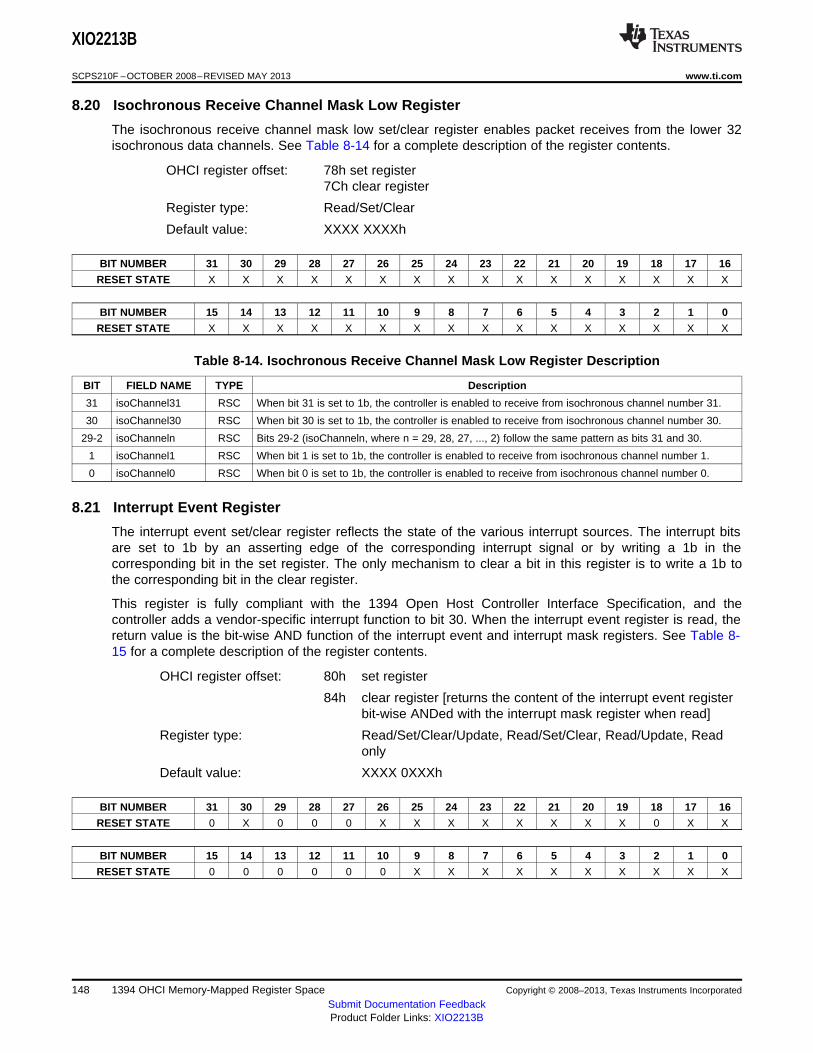
XIO2213B
SCPS210F –OCTOBER 2008–REVISED MAY 2013 www.ti.com
8.20 Isochronous Receive Channel Mask Low Register
The isochronous receive channel mask low set/clear register enables packet receives from the lower 32isochronous data channels. See Table 8-14 for a complete description of the register contents.
OHCI register offset: 78h set register7Ch clear register
Register type: Read/Set/Clear
Default value: XXXX XXXXh
BIT NUMBER 31 30 29 28 27 26 25 24 23 22 21 20 19 18 17 16
RESET STATE X X X X X X X X X X X X X X X X
BIT NUMBER 15 14 13 12 11 10 9 8 7 6 5 4 3 2 1 0
RESET STATE X X X X X X X X X X X X X X X X
Table 8-14. Isochronous Receive Channel Mask Low Register Description
BIT FIELD NAME TYPE Description
31 isoChannel31 RSC When bit 31 is set to 1b, the controller is enabled to receive from isochronous channel number 31.
30 isoChannel30 RSC When bit 30 is set to 1b, the controller is enabled to receive from isochronous channel number 30.
29-2 isoChanneln RSC Bits 29-2 (isoChanneln, where n = 29, 28, 27, ..., 2) follow the same pattern as bits 31 and 30.
1 isoChannel1 RSC When bit 1 is set to 1b, the controller is enabled to receive from isochronous channel number 1.
0 isoChannel0 RSC When bit 0 is set to 1b, the controller is enabled to receive from isochronous channel number 0.
8.21 Interrupt Event Register
The interrupt event set/clear register reflects the state of the various interrupt sources. The interrupt bitsare set to 1b by an asserting edge of the corresponding interrupt signal or by writing a 1b in thecorresponding bit in the set register. The only mechanism to clear a bit in this register is to write a 1b tothe corresponding bit in the clear register.
This register is fully compliant with the 1394 Open Host Controller Interface Specification, and thecontroller adds a vendor-specific interrupt function to bit 30. When the interrupt event register is read, thereturn value is the bit-wise AND function of the interrupt event and interrupt mask registers. See Table 8-15 for a complete description of the register contents.
OHCI register offset: 80h set register
84h clear register [returns the content of the interrupt event registerbit-wise ANDed with the interrupt mask register when read]
Register type: Read/Set/Clear/Update, Read/Set/Clear, Read/Update, Readonly
Default value: XXXX 0XXXh
BIT NUMBER 31 30 29 28 27 26 25 24 23 22 21 20 19 18 17 16
RESET STATE 0 X 0 0 0 X X X X X X X X 0 X X
BIT NUMBER 15 14 13 12 11 10 9 8 7 6 5 4 3 2 1 0
RESET STATE 0 0 0 0 0 0 X X X X X X X X X X
148 1394 OHCI Memory-Mapped Register Space Copyright © 2008–2013, Texas Instruments Incorporated
Submit Documentation FeedbackProduct Folder Links: XIO2213B
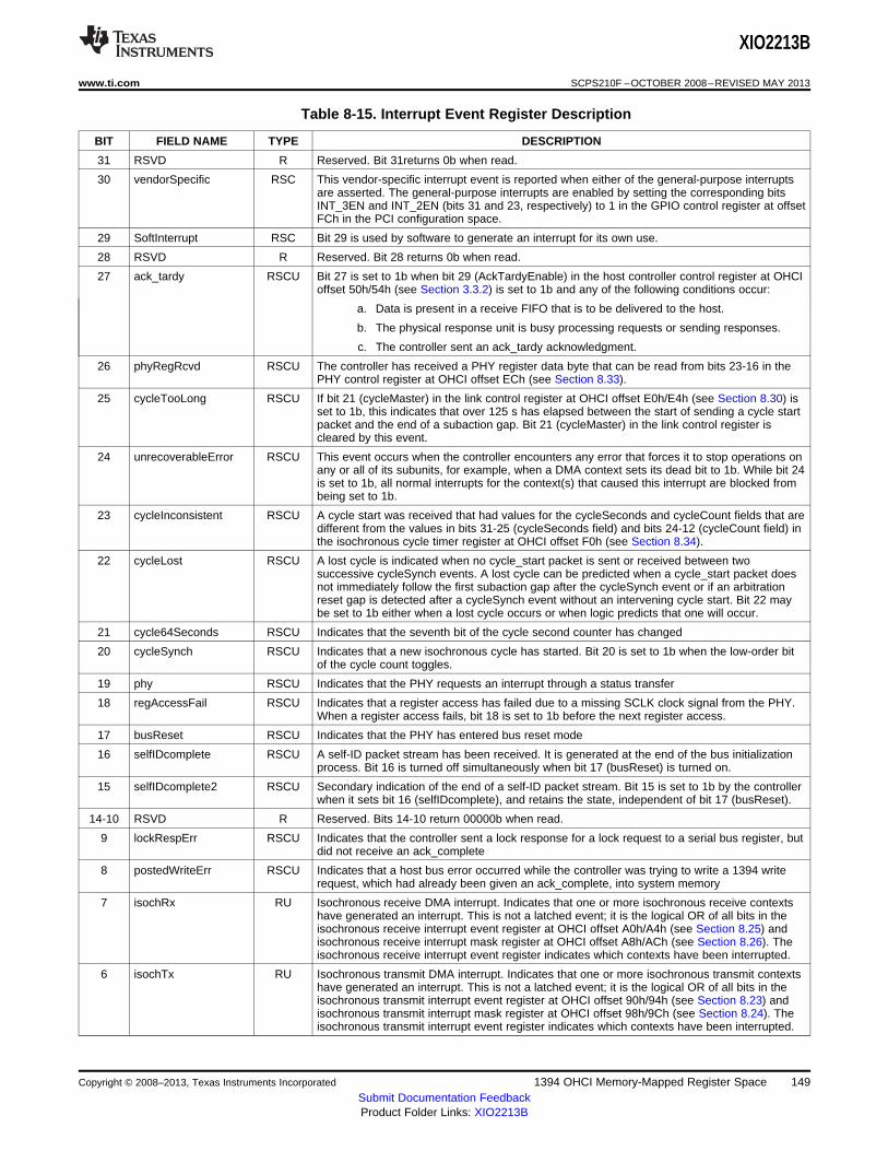
XIO2213B
www.ti.com SCPS210F –OCTOBER 2008–REVISED MAY 2013
Table 8-15. Interrupt Event Register Description
BIT FIELD NAME TYPE DESCRIPTION
31 RSVD R Reserved. Bit 31returns 0b when read.
30 vendorSpecific RSC This vendor-specific interrupt event is reported when either of the general-purpose interruptsare asserted. The general-purpose interrupts are enabled by setting the corresponding bitsINT_3EN and INT_2EN (bits 31 and 23, respectively) to 1 in the GPIO control register at offsetFCh in the PCI configuration space.
29 SoftInterrupt RSC Bit 29 is used by software to generate an interrupt for its own use.
28 RSVD R Reserved. Bit 28 returns 0b when read.
27 ack_tardy RSCU Bit 27 is set to 1b when bit 29 (AckTardyEnable) in the host controller control register at OHCIoffset 50h/54h (see Section 3.3.2) is set to 1b and any of the following conditions occur:
a. Data is present in a receive FIFO that is to be delivered to the host.
b. The physical response unit is busy processing requests or sending responses.
c. The controller sent an ack_tardy acknowledgment.
26 phyRegRcvd RSCU The controller has received a PHY register data byte that can be read from bits 23-16 in thePHY control register at OHCI offset ECh (see Section 8.33).
25 cycleTooLong RSCU If bit 21 (cycleMaster) in the link control register at OHCI offset E0h/E4h (see Section 8.30) isset to 1b, this indicates that over 125 s has elapsed between the start of sending a cycle startpacket and the end of a subaction gap. Bit 21 (cycleMaster) in the link control register iscleared by this event.
24 unrecoverableError RSCU This event occurs when the controller encounters any error that forces it to stop operations onany or all of its subunits, for example, when a DMA context sets its dead bit to 1b. While bit 24is set to 1b, all normal interrupts for the context(s) that caused this interrupt are blocked frombeing set to 1b.
23 cycleInconsistent RSCU A cycle start was received that had values for the cycleSeconds and cycleCount fields that aredifferent from the values in bits 31-25 (cycleSeconds field) and bits 24-12 (cycleCount field) inthe isochronous cycle timer register at OHCI offset F0h (see Section 8.34).
22 cycleLost RSCU A lost cycle is indicated when no cycle_start packet is sent or received between twosuccessive cycleSynch events. A lost cycle can be predicted when a cycle_start packet doesnot immediately follow the first subaction gap after the cycleSynch event or if an arbitrationreset gap is detected after a cycleSynch event without an intervening cycle start. Bit 22 maybe set to 1b either when a lost cycle occurs or when logic predicts that one will occur.
21 cycle64Seconds RSCU Indicates that the seventh bit of the cycle second counter has changed
20 cycleSynch RSCU Indicates that a new isochronous cycle has started. Bit 20 is set to 1b when the low-order bitof the cycle count toggles.
19 phy RSCU Indicates that the PHY requests an interrupt through a status transfer
18 regAccessFail RSCU Indicates that a register access has failed due to a missing SCLK clock signal from the PHY.When a register access fails, bit 18 is set to 1b before the next register access.
17 busReset RSCU Indicates that the PHY has entered bus reset mode
16 selfIDcomplete RSCU A self-ID packet stream has been received. It is generated at the end of the bus initializationprocess. Bit 16 is turned off simultaneously when bit 17 (busReset) is turned on.
15 selfIDcomplete2 RSCU Secondary indication of the end of a self-ID packet stream. Bit 15 is set to 1b by the controllerwhen it sets bit 16 (selfIDcomplete), and retains the state, independent of bit 17 (busReset).
14-10 RSVD R Reserved. Bits 14-10 return 00000b when read.
9 lockRespErr RSCU Indicates that the controller sent a lock response for a lock request to a serial bus register, butdid not receive an ack_complete
8 postedWriteErr RSCU Indicates that a host bus error occurred while the controller was trying to write a 1394 writerequest, which had already been given an ack_complete, into system memory
7 isochRx RU Isochronous receive DMA interrupt. Indicates that one or more isochronous receive contextshave generated an interrupt. This is not a latched event; it is the logical OR of all bits in theisochronous receive interrupt event register at OHCI offset A0h/A4h (see Section 8.25) andisochronous receive interrupt mask register at OHCI offset A8h/ACh (see Section 8.26). Theisochronous receive interrupt event register indicates which contexts have been interrupted.
6 isochTx RU Isochronous transmit DMA interrupt. Indicates that one or more isochronous transmit contextshave generated an interrupt. This is not a latched event; it is the logical OR of all bits in theisochronous transmit interrupt event register at OHCI offset 90h/94h (see Section 8.23) andisochronous transmit interrupt mask register at OHCI offset 98h/9Ch (see Section 8.24). Theisochronous transmit interrupt event register indicates which contexts have been interrupted.
Copyright © 2008–2013, Texas Instruments Incorporated 1394 OHCI Memory-Mapped Register Space 149Submit Documentation FeedbackProduct Folder Links: XIO2213B
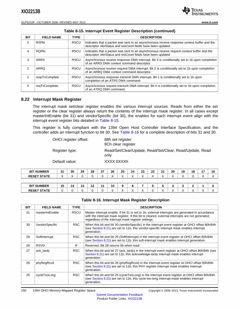
XIO2213B
SCPS210F –OCTOBER 2008–REVISED MAY 2013 www.ti.com
Table 8-15. Interrupt Event Register Description (continued)
BIT FIELD NAME TYPE DESCRIPTION
5 RSPkt RSCU Indicates that a packet was sent to an asynchronous receive response context buffer and thedescriptor xferStatus and resCount fields have been updated
4 RQPkt RSCU Indicates that a packet was sent to an asynchronous receive request context buffer and thedescriptor xferStatus and resCount fields have been updated
3 ARRS RSCU Asynchronous receive response DMA interrupt. Bit 3 is conditionally set to 1b upon completionof an ARRS DMA context command descriptor.
2 ARRQ RSCU Asynchronous receive request DMA interrupt. Bit 2 is conditionally set to 1b upon completionof an ARRQ DMA context command descriptor.
1 respTxComplete RSCU Asynchronous response transmit DMA interrupt. Bit 1 is conditionally set to 1b uponcompletion of an ATRS DMA command.
0 reqTxCompleter RSCU Asynchronous request transmit DMA interrupt. Bit 0 is conditionally set to 1b upon completionof an ATRQ DMA command.
8.22 Interrupt Mask Register
The interrupt mask set/clear register enables the various interrupt sources. Reads from either the setregister or the clear register always return the contents of the interrupt mask register. In all cases exceptmasterIntEnable (bit 31) and vendorSpecific (bit 30), the enables for each interrupt event align with theinterrupt event register bits detailed in Table 8-15.
This register is fully compliant with the 1394 Open Host Controller Interface Specification, and thecontroller adds an interrupt function to bit 30. See Table 8-16 for a complete description of bits 31 and 30.
OHCI register offset: 88h set register8Ch clear register
Register type: Read/Set/Clear/Update, Read/Set/Clear, Read/Update, Readonly
Default value: XXXX 0XXXh
BIT NUMBER 31 30 29 28 27 26 25 24 23 22 21 20 19 18 17 16
RESET STATE X X 0 0 0 X X X X X X X X 0 X X
BIT NUMBER 15 14 13 12 11 10 9 8 7 6 5 4 3 2 1 0
RESET STATE 0 0 0 0 0 0 X X X X X X X X X X
Table 8-16. Interrupt Mask Register Description
BIT FIELD NAME TYPE DESCRIPTION
31 masterIntEnable RSCU Master interrupt enable. If bit 31 is set to 1b, external interrupts are generated in accordancewith the interrupt mask register. If this bit is cleared, external interrupts are not generated,regardless of the interrupt mask register settings.
30 VendorSpecific RSC When this bit and bit 30 (vendorSpecific) in the interrupt event register at OHCI offset 80h/84h(see Section 8.21) are set to 11b, this vendor-specific interrupt mask enables interruptgeneration.
29 SoftInterrupt RSC When this bit and bit 29 (SoftInterrupt) in the interrupt event register at OHCI offset 80h/84h(see Section 8.21) are set to 11b, this soft-interrupt mask enables interrupt generation.
28 RSVD R Reserved. Bit 28 returns 0b when read.
27 ack_tardy RSC When this bit and bit 27 (ack_tardy) in the interrupt event register at OHCI offset 80h/84h (seeSection 8.21) are set to 11b, this acknowledge-tardy interrupt mask enables interruptgeneration.
26 phyRegRcvd RSC When this bit and bit 26 (phyRegRcvd) in the interrupt event register at OHCI offset 80h/84h(see Section 8.21) are set to 11b, this PHY register interrupt mask enables interruptgeneration.
25 cycleTooLong RSC When this bit and bit 25 (cycleTooLong) in the interrupt event register at OHCI offset 80h/84h(see Section 8.21) are set to 11b, this cycle-too-long interrupt mask enables interruptgeneration.
150 1394 OHCI Memory-Mapped Register Space Copyright © 2008–2013, Texas Instruments Incorporated
Submit Documentation FeedbackProduct Folder Links: XIO2213B
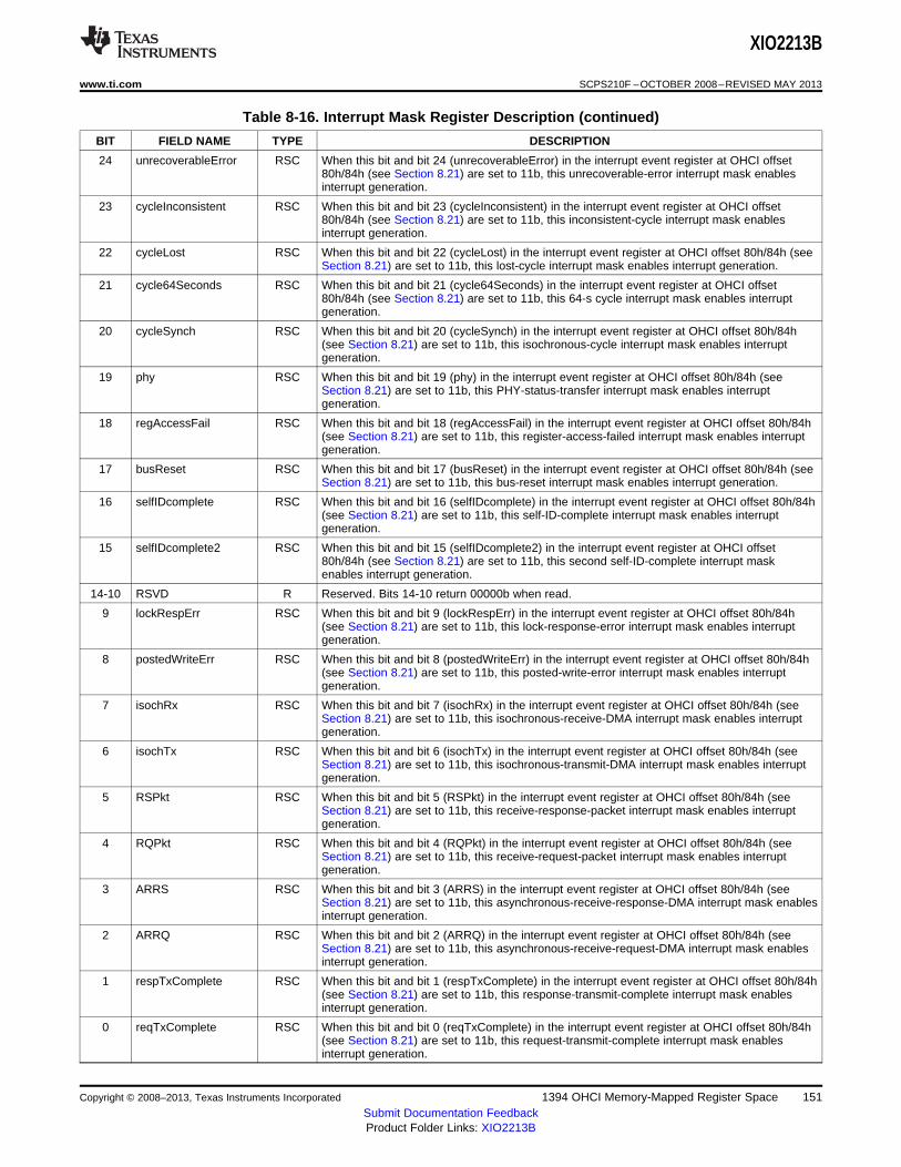
XIO2213B
www.ti.com SCPS210F –OCTOBER 2008–REVISED MAY 2013
Table 8-16. Interrupt Mask Register Description (continued)
BIT FIELD NAME TYPE DESCRIPTION
24 unrecoverableError RSC When this bit and bit 24 (unrecoverableError) in the interrupt event register at OHCI offset80h/84h (see Section 8.21) are set to 11b, this unrecoverable-error interrupt mask enablesinterrupt generation.
23 cycleInconsistent RSC When this bit and bit 23 (cycleInconsistent) in the interrupt event register at OHCI offset80h/84h (see Section 8.21) are set to 11b, this inconsistent-cycle interrupt mask enablesinterrupt generation.
22 cycleLost RSC When this bit and bit 22 (cycleLost) in the interrupt event register at OHCI offset 80h/84h (seeSection 8.21) are set to 11b, this lost-cycle interrupt mask enables interrupt generation.
21 cycle64Seconds RSC When this bit and bit 21 (cycle64Seconds) in the interrupt event register at OHCI offset80h/84h (see Section 8.21) are set to 11b, this 64-s cycle interrupt mask enables interruptgeneration.
20 cycleSynch RSC When this bit and bit 20 (cycleSynch) in the interrupt event register at OHCI offset 80h/84h(see Section 8.21) are set to 11b, this isochronous-cycle interrupt mask enables interruptgeneration.
19 phy RSC When this bit and bit 19 (phy) in the interrupt event register at OHCI offset 80h/84h (seeSection 8.21) are set to 11b, this PHY-status-transfer interrupt mask enables interruptgeneration.
18 regAccessFail RSC When this bit and bit 18 (regAccessFail) in the interrupt event register at OHCI offset 80h/84h(see Section 8.21) are set to 11b, this register-access-failed interrupt mask enables interruptgeneration.
17 busReset RSC When this bit and bit 17 (busReset) in the interrupt event register at OHCI offset 80h/84h (seeSection 8.21) are set to 11b, this bus-reset interrupt mask enables interrupt generation.
16 selfIDcomplete RSC When this bit and bit 16 (selfIDcomplete) in the interrupt event register at OHCI offset 80h/84h(see Section 8.21) are set to 11b, this self-ID-complete interrupt mask enables interruptgeneration.
15 selfIDcomplete2 RSC When this bit and bit 15 (selfIDcomplete2) in the interrupt event register at OHCI offset80h/84h (see Section 8.21) are set to 11b, this second self-ID-complete interrupt maskenables interrupt generation.
14-10 RSVD R Reserved. Bits 14-10 return 00000b when read.
9 lockRespErr RSC When this bit and bit 9 (lockRespErr) in the interrupt event register at OHCI offset 80h/84h(see Section 8.21) are set to 11b, this lock-response-error interrupt mask enables interruptgeneration.
8 postedWriteErr RSC When this bit and bit 8 (postedWriteErr) in the interrupt event register at OHCI offset 80h/84h(see Section 8.21) are set to 11b, this posted-write-error interrupt mask enables interruptgeneration.
7 isochRx RSC When this bit and bit 7 (isochRx) in the interrupt event register at OHCI offset 80h/84h (seeSection 8.21) are set to 11b, this isochronous-receive-DMA interrupt mask enables interruptgeneration.
6 isochTx RSC When this bit and bit 6 (isochTx) in the interrupt event register at OHCI offset 80h/84h (seeSection 8.21) are set to 11b, this isochronous-transmit-DMA interrupt mask enables interruptgeneration.
5 RSPkt RSC When this bit and bit 5 (RSPkt) in the interrupt event register at OHCI offset 80h/84h (seeSection 8.21) are set to 11b, this receive-response-packet interrupt mask enables interruptgeneration.
4 RQPkt RSC When this bit and bit 4 (RQPkt) in the interrupt event register at OHCI offset 80h/84h (seeSection 8.21) are set to 11b, this receive-request-packet interrupt mask enables interruptgeneration.
3 ARRS RSC When this bit and bit 3 (ARRS) in the interrupt event register at OHCI offset 80h/84h (seeSection 8.21) are set to 11b, this asynchronous-receive-response-DMA interrupt mask enablesinterrupt generation.
2 ARRQ RSC When this bit and bit 2 (ARRQ) in the interrupt event register at OHCI offset 80h/84h (seeSection 8.21) are set to 11b, this asynchronous-receive-request-DMA interrupt mask enablesinterrupt generation.
1 respTxComplete RSC When this bit and bit 1 (respTxComplete) in the interrupt event register at OHCI offset 80h/84h(see Section 8.21) are set to 11b, this response-transmit-complete interrupt mask enablesinterrupt generation.
0 reqTxComplete RSC When this bit and bit 0 (reqTxComplete) in the interrupt event register at OHCI offset 80h/84h(see Section 8.21) are set to 11b, this request-transmit-complete interrupt mask enablesinterrupt generation.
Copyright © 2008–2013, Texas Instruments Incorporated 1394 OHCI Memory-Mapped Register Space 151Submit Documentation FeedbackProduct Folder Links: XIO2213B
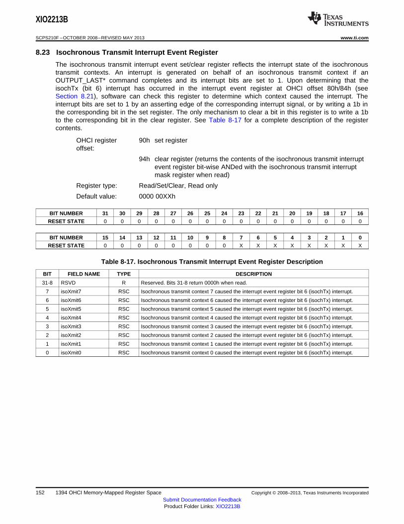
XIO2213B
SCPS210F –OCTOBER 2008–REVISED MAY 2013 www.ti.com
8.23 Isochronous Transmit Interrupt Event Register
The isochronous transmit interrupt event set/clear register reflects the interrupt state of the isochronoustransmit contexts. An interrupt is generated on behalf of an isochronous transmit context if anOUTPUT_LAST* command completes and its interrupt bits are set to 1. Upon determining that theisochTx (bit 6) interrupt has occurred in the interrupt event register at OHCI offset 80h/84h (seeSection 8.21), software can check this register to determine which context caused the interrupt. Theinterrupt bits are set to 1 by an asserting edge of the corresponding interrupt signal, or by writing a 1b inthe corresponding bit in the set register. The only mechanism to clear a bit in this register is to write a 1bto the corresponding bit in the clear register. See Table 8-17 for a complete description of the registercontents.
OHCI register 90h set registeroffset:
94h clear register (returns the contents of the isochronous transmit interruptevent register bit-wise ANDed with the isochronous transmit interruptmask register when read)
Register type: Read/Set/Clear, Read only
Default value: 0000 00XXh
BIT NUMBER 31 30 29 28 27 26 25 24 23 22 21 20 19 18 17 16
RESET STATE 0 0 0 0 0 0 0 0 0 0 0 0 0 0 0 0
BIT NUMBER 15 14 13 12 11 10 9 8 7 6 5 4 3 2 1 0
RESET STATE 0 0 0 0 0 0 0 0 X X X X X X X X
Table 8-17. Isochronous Transmit Interrupt Event Register Description
BIT FIELD NAME TYPE DESCRIPTION
31-8 RSVD R Reserved. Bits 31-8 return 0000h when read.
7 isoXmit7 RSC Isochronous transmit context 7 caused the interrupt event register bit 6 (isochTx) interrupt.
6 isoXmit6 RSC Isochronous transmit context 6 caused the interrupt event register bit 6 (isochTx) interrupt.
5 isoXmit5 RSC Isochronous transmit context 5 caused the interrupt event register bit 6 (isochTx) interrupt.
4 isoXmit4 RSC Isochronous transmit context 4 caused the interrupt event register bit 6 (isochTx) interrupt.
3 isoXmit3 RSC Isochronous transmit context 3 caused the interrupt event register bit 6 (isochTx) interrupt.
2 isoXmit2 RSC Isochronous transmit context 2 caused the interrupt event register bit 6 (isochTx) interrupt.
1 isoXmit1 RSC Isochronous transmit context 1 caused the interrupt event register bit 6 (isochTx) interrupt.
0 isoXmit0 RSC Isochronous transmit context 0 caused the interrupt event register bit 6 (isochTx) interrupt.
152 1394 OHCI Memory-Mapped Register Space Copyright © 2008–2013, Texas Instruments Incorporated
Submit Documentation FeedbackProduct Folder Links: XIO2213B
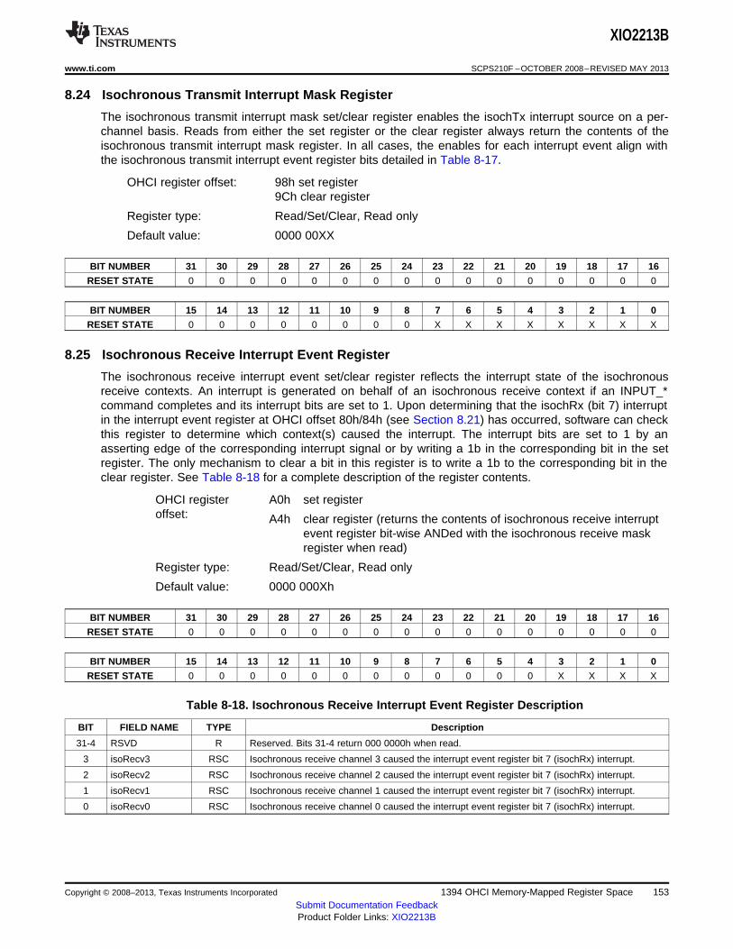
XIO2213B
www.ti.com SCPS210F –OCTOBER 2008–REVISED MAY 2013
8.24 Isochronous Transmit Interrupt Mask Register
The isochronous transmit interrupt mask set/clear register enables the isochTx interrupt source on a per-channel basis. Reads from either the set register or the clear register always return the contents of theisochronous transmit interrupt mask register. In all cases, the enables for each interrupt event align withthe isochronous transmit interrupt event register bits detailed in Table 8-17.
OHCI register offset: 98h set register9Ch clear register
Register type: Read/Set/Clear, Read only
Default value: 0000 00XX
BIT NUMBER 31 30 29 28 27 26 25 24 23 22 21 20 19 18 17 16
RESET STATE 0 0 0 0 0 0 0 0 0 0 0 0 0 0 0 0
BIT NUMBER 15 14 13 12 11 10 9 8 7 6 5 4 3 2 1 0
RESET STATE 0 0 0 0 0 0 0 0 X X X X X X X X
8.25 Isochronous Receive Interrupt Event Register
The isochronous receive interrupt event set/clear register reflects the interrupt state of the isochronousreceive contexts. An interrupt is generated on behalf of an isochronous receive context if an INPUT_*command completes and its interrupt bits are set to 1. Upon determining that the isochRx (bit 7) interruptin the interrupt event register at OHCI offset 80h/84h (see Section 8.21) has occurred, software can checkthis register to determine which context(s) caused the interrupt. The interrupt bits are set to 1 by anasserting edge of the corresponding interrupt signal or by writing a 1b in the corresponding bit in the setregister. The only mechanism to clear a bit in this register is to write a 1b to the corresponding bit in theclear register. See Table 8-18 for a complete description of the register contents.
OHCI register A0h set registeroffset: A4h clear register (returns the contents of isochronous receive interrupt
event register bit-wise ANDed with the isochronous receive maskregister when read)
Register type: Read/Set/Clear, Read only
Default value: 0000 000Xh
BIT NUMBER 31 30 29 28 27 26 25 24 23 22 21 20 19 18 17 16
RESET STATE 0 0 0 0 0 0 0 0 0 0 0 0 0 0 0 0
BIT NUMBER 15 14 13 12 11 10 9 8 7 6 5 4 3 2 1 0
RESET STATE 0 0 0 0 0 0 0 0 0 0 0 0 X X X X
Table 8-18. Isochronous Receive Interrupt Event Register Description
BIT FIELD NAME TYPE Description
31-4 RSVD R Reserved. Bits 31-4 return 000 0000h when read.
3 isoRecv3 RSC Isochronous receive channel 3 caused the interrupt event register bit 7 (isochRx) interrupt.
2 isoRecv2 RSC Isochronous receive channel 2 caused the interrupt event register bit 7 (isochRx) interrupt.
1 isoRecv1 RSC Isochronous receive channel 1 caused the interrupt event register bit 7 (isochRx) interrupt.
0 isoRecv0 RSC Isochronous receive channel 0 caused the interrupt event register bit 7 (isochRx) interrupt.
Copyright © 2008–2013, Texas Instruments Incorporated 1394 OHCI Memory-Mapped Register Space 153Submit Documentation FeedbackProduct Folder Links: XIO2213B
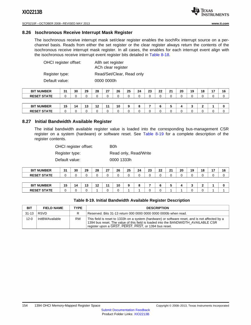
XIO2213B
SCPS210F –OCTOBER 2008–REVISED MAY 2013 www.ti.com
8.26 Isochronous Receive Interrupt Mask Register
The isochronous receive interrupt mask set/clear register enables the isochRx interrupt source on a per-channel basis. Reads from either the set register or the clear register always return the contents of theisochronous receive interrupt mask register. In all cases, the enables for each interrupt event align withthe isochronous receive interrupt event register bits detailed in Table 8-18.
OHCI register offset: A8h set registerACh clear register
Register type: Read/Set/Clear, Read only
Default value: 0000 0000h
BIT NUMBER 31 30 29 28 27 26 25 24 23 22 21 20 19 18 17 16
RESET STATE 0 0 0 0 0 0 0 0 0 0 0 0 0 0 0 0
BIT NUMBER 15 14 13 12 11 10 9 8 7 6 5 4 3 2 1 0
RESET STATE 0 0 0 0 0 0 0 0 0 0 0 0 0 0 0 0
8.27 Initial Bandwidth Available Register
The initial bandwidth available register value is loaded into the corresponding bus-management CSRregister on a system (hardware) or software reset. See Table 8-19 for a complete description of theregister contents.
OHCI register offset: B0h
Register type: Read only, Read/Write
Default value: 0000 1333h
BIT NUMBER 31 30 29 28 27 26 25 24 23 22 21 20 19 18 17 16
RESET STATE 0 0 0 0 0 0 0 0 0 0 0 0 0 0 0 0
BIT NUMBER 15 14 13 12 11 10 9 8 7 6 5 4 3 2 1 0
RESET STATE 0 0 0 1 0 0 1 1 0 0 1 1 0 0 1 1
Table 8-19. Initial Bandwidth Available Register Description
BIT FIELD NAME TYPE DESCRIPTION
31-13 RSVD R Reserved. Bits 31-13 return 000 0000 0000 0000 0000b when read.
12-0 InitBWAvailable RW This field is reset to 1333h on a system (hardware) or software reset, and is not affected by a1394 bus reset. The value of this field is loaded into the BANDWIDTH_AVAILABLE CSRregister upon a GRST, PERST, PRST, or 1394 bus reset.
154 1394 OHCI Memory-Mapped Register Space Copyright © 2008–2013, Texas Instruments Incorporated
Submit Documentation FeedbackProduct Folder Links: XIO2213B
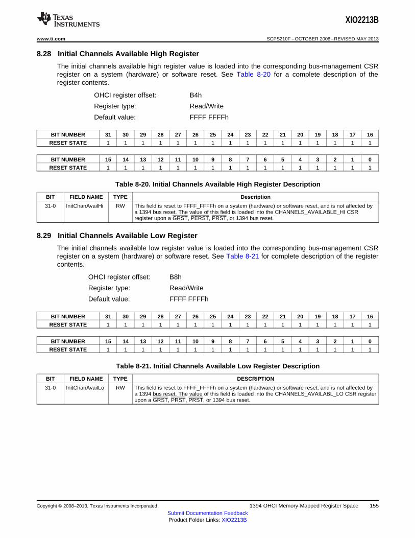
XIO2213B
www.ti.com SCPS210F –OCTOBER 2008–REVISED MAY 2013
8.28 Initial Channels Available High Register
The initial channels available high register value is loaded into the corresponding bus-management CSRregister on a system (hardware) or software reset. See Table 8-20 for a complete description of theregister contents.
OHCI register offset: B4h
Register type: Read/Write
Default value: FFFF FFFFh
BIT NUMBER 31 30 29 28 27 26 25 24 23 22 21 20 19 18 17 16
RESET STATE 1 1 1 1 1 1 1 1 1 1 1 1 1 1 1 1
BIT NUMBER 15 14 13 12 11 10 9 8 7 6 5 4 3 2 1 0
RESET STATE 1 1 1 1 1 1 1 1 1 1 1 1 1 1 1 1
Table 8-20. Initial Channels Available High Register Description
BIT FIELD NAME TYPE Description
31-0 InitChanAvailHi RW This field is reset to FFFF_FFFFh on a system (hardware) or software reset, and is not affected bya 1394 bus reset. The value of this field is loaded into the CHANNELS_AVAILABLE_HI CSRregister upon a GRST, PERST, PRST, or 1394 bus reset.
8.29 Initial Channels Available Low Register
The initial channels available low register value is loaded into the corresponding bus-management CSRregister on a system (hardware) or software reset. See Table 8-21 for complete description of the registercontents.
OHCI register offset: B8h
Register type: Read/Write
Default value: FFFF FFFFh
BIT NUMBER 31 30 29 28 27 26 25 24 23 22 21 20 19 18 17 16
RESET STATE 1 1 1 1 1 1 1 1 1 1 1 1 1 1 1 1
BIT NUMBER 15 14 13 12 11 10 9 8 7 6 5 4 3 2 1 0
RESET STATE 1 1 1 1 1 1 1 1 1 1 1 1 1 1 1 1
Table 8-21. Initial Channels Available Low Register Description
BIT FIELD NAME TYPE DESCRIPTION
31-0 InitChanAvailLo RW This field is reset to FFFF_FFFFh on a system (hardware) or software reset, and is not affected bya 1394 bus reset. The value of this field is loaded into the CHANNELS_AVAILABL_LO CSR registerupon a GRST, PRST, PRST, or 1394 bus reset.
Copyright © 2008–2013, Texas Instruments Incorporated 1394 OHCI Memory-Mapped Register Space 155Submit Documentation FeedbackProduct Folder Links: XIO2213B
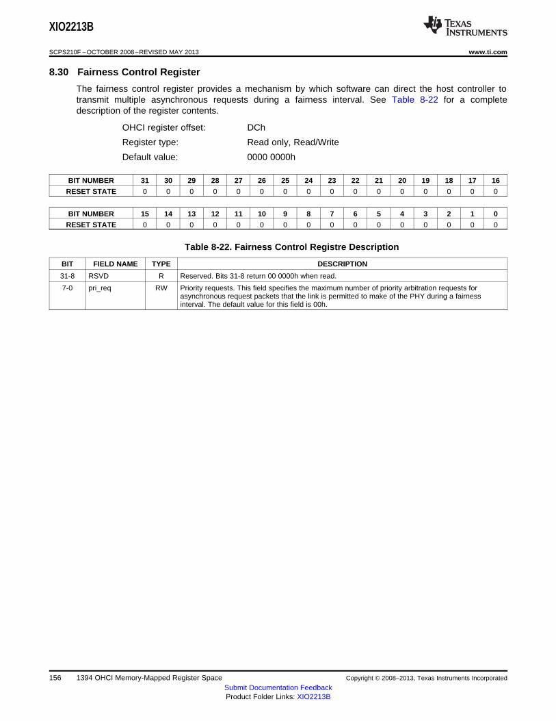
XIO2213B
SCPS210F –OCTOBER 2008–REVISED MAY 2013 www.ti.com
8.30 Fairness Control Register
The fairness control register provides a mechanism by which software can direct the host controller totransmit multiple asynchronous requests during a fairness interval. See Table 8-22 for a completedescription of the register contents.
OHCI register offset: DCh
Register type: Read only, Read/Write
Default value: 0000 0000h
BIT NUMBER 31 30 29 28 27 26 25 24 23 22 21 20 19 18 17 16
RESET STATE 0 0 0 0 0 0 0 0 0 0 0 0 0 0 0 0
BIT NUMBER 15 14 13 12 11 10 9 8 7 6 5 4 3 2 1 0
RESET STATE 0 0 0 0 0 0 0 0 0 0 0 0 0 0 0 0
Table 8-22. Fairness Control Registre Description
BIT FIELD NAME TYPE DESCRIPTION
31-8 RSVD R Reserved. Bits 31-8 return 00 0000h when read.
7-0 pri_req RW Priority requests. This field specifies the maximum number of priority arbitration requests forasynchronous request packets that the link is permitted to make of the PHY during a fairnessinterval. The default value for this field is 00h.
156 1394 OHCI Memory-Mapped Register Space Copyright © 2008–2013, Texas Instruments Incorporated
Submit Documentation FeedbackProduct Folder Links: XIO2213B
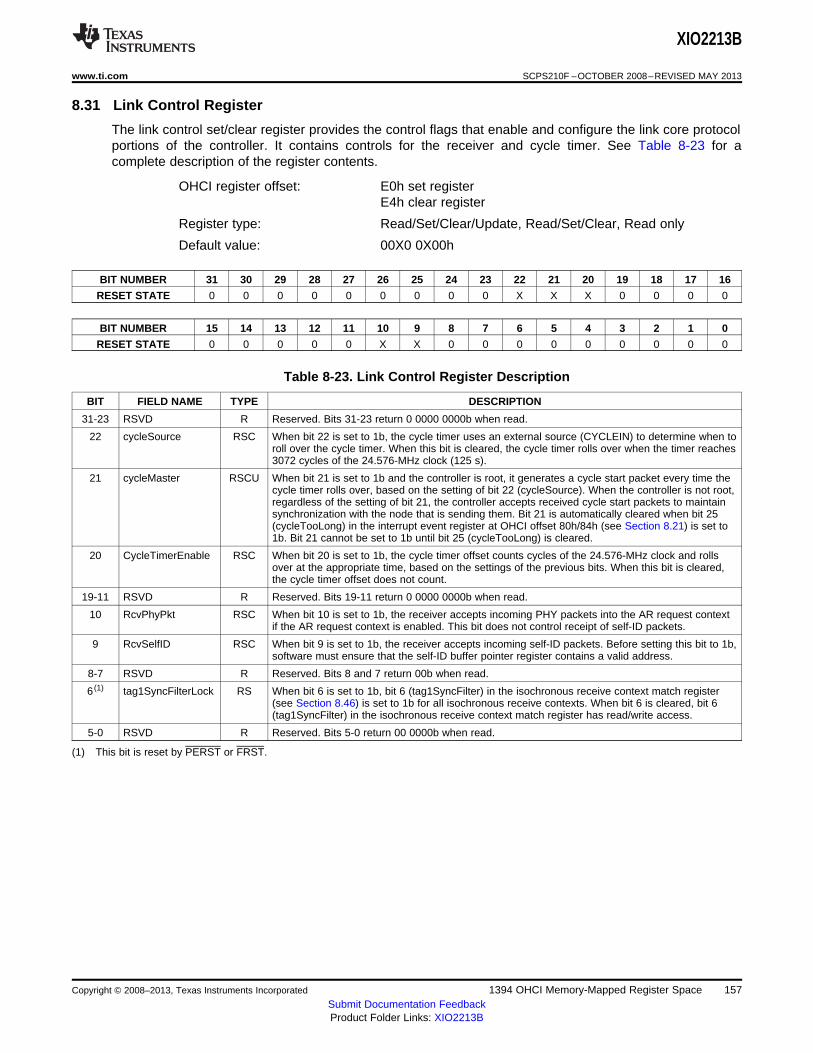
XIO2213B
www.ti.com SCPS210F –OCTOBER 2008–REVISED MAY 2013
8.31 Link Control Register
The link control set/clear register provides the control flags that enable and configure the link core protocolportions of the controller. It contains controls for the receiver and cycle timer. See Table 8-23 for acomplete description of the register contents.
OHCI register offset: E0h set registerE4h clear register
Register type: Read/Set/Clear/Update, Read/Set/Clear, Read only
Default value: 00X0 0X00h
BIT NUMBER 31 30 29 28 27 26 25 24 23 22 21 20 19 18 17 16
RESET STATE 0 0 0 0 0 0 0 0 0 X X X 0 0 0 0
BIT NUMBER 15 14 13 12 11 10 9 8 7 6 5 4 3 2 1 0
RESET STATE 0 0 0 0 0 X X 0 0 0 0 0 0 0 0 0
Table 8-23. Link Control Register Description
BIT FIELD NAME TYPE DESCRIPTION
31-23 RSVD R Reserved. Bits 31-23 return 0 0000 0000b when read.
22 cycleSource RSC When bit 22 is set to 1b, the cycle timer uses an external source (CYCLEIN) to determine when toroll over the cycle timer. When this bit is cleared, the cycle timer rolls over when the timer reaches3072 cycles of the 24.576-MHz clock (125 s).
21 cycleMaster RSCU When bit 21 is set to 1b and the controller is root, it generates a cycle start packet every time thecycle timer rolls over, based on the setting of bit 22 (cycleSource). When the controller is not root,regardless of the setting of bit 21, the controller accepts received cycle start packets to maintainsynchronization with the node that is sending them. Bit 21 is automatically cleared when bit 25(cycleTooLong) in the interrupt event register at OHCI offset 80h/84h (see Section 8.21) is set to1b. Bit 21 cannot be set to 1b until bit 25 (cycleTooLong) is cleared.
20 CycleTimerEnable RSC When bit 20 is set to 1b, the cycle timer offset counts cycles of the 24.576-MHz clock and rollsover at the appropriate time, based on the settings of the previous bits. When this bit is cleared,the cycle timer offset does not count.
19-11 RSVD R Reserved. Bits 19-11 return 0 0000 0000b when read.
10 RcvPhyPkt RSC When bit 10 is set to 1b, the receiver accepts incoming PHY packets into the AR request contextif the AR request context is enabled. This bit does not control receipt of self-ID packets.
9 RcvSelfID RSC When bit 9 is set to 1b, the receiver accepts incoming self-ID packets. Before setting this bit to 1b,software must ensure that the self-ID buffer pointer register contains a valid address.
8-7 RSVD R Reserved. Bits 8 and 7 return 00b when read.
6 (1) tag1SyncFilterLock RS When bit 6 is set to 1b, bit 6 (tag1SyncFilter) in the isochronous receive context match register(see Section 8.46) is set to 1b for all isochronous receive contexts. When bit 6 is cleared, bit 6(tag1SyncFilter) in the isochronous receive context match register has read/write access.
5-0 RSVD R Reserved. Bits 5-0 return 00 0000b when read.
(1) This bit is reset by PERST or FRST.
Copyright © 2008–2013, Texas Instruments Incorporated 1394 OHCI Memory-Mapped Register Space 157Submit Documentation FeedbackProduct Folder Links: XIO2213B
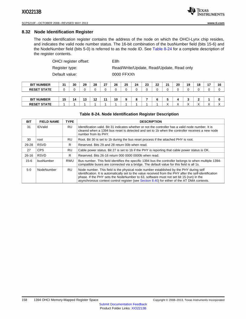
XIO2213B
SCPS210F –OCTOBER 2008–REVISED MAY 2013 www.ti.com
8.32 Node Identification Register
The node identification register contains the address of the node on which the OHCI-Lynx chip resides,and indicates the valid node number status. The 16-bit combination of the busNumber field (bits 15-6) andthe NodeNumber field (bits 5-0) is referred to as the node ID. See Table 8-24 for a complete description ofthe register contents.
OHCI register offset: E8h
Register type: Read/Write/Update, Read/Update, Read only
Default value: 0000 FFXXh
BIT NUMBER 31 30 29 28 27 26 25 24 23 22 21 20 19 18 17 16
RESET STATE 0 0 0 0 0 0 0 0 0 0 0 0 0 0 0 0
BIT NUMBER 15 14 13 12 11 10 9 8 7 6 5 4 3 2 1 0
RESET STATE 1 1 1 1 1 1 1 1 1 1 X X X X X X
Table 8-24. Node Identification Register Description
BIT FIELD NAME TYPE DESCRIPTION
31 IDValid RU Identification valid. Bit 31 indicates whether or not the controller has a valid node number. It iscleared when a 1394 bus reset is detected and set to 1b when the controller receives a new nodenumber from its PHY.
30 root RU Root. Bit 30 is set to 1b during the bus reset process if the attached PHY is root.
29-28 RSVD R Reserved. Bits 29 and 28 return 00b when read.
27 CPS RU Cable power status. Bit 27 is set to 1b if the PHY is reporting that cable power status is OK.
26-16 RSVD R Reserved. Bits 26-16 return 000 0000 0000b when read.
15-6 busNumber RWU Bus number. This field identifies the specific 1394 bus the controller belongs to when multiple 1394-compatible buses are connected via a bridge. The default value for this field is all 1s.
5-0 NodeNumber RU Node number. This field is the physical node number established by the PHY during selfidentification. It is automatically set to the value received from the PHY after the self-identificationphase. If the PHY sets the NodeNumber to 63, software must not set bit 15 (run) in theasynchronous context control register (see Section 8.40) for either of the AT DMA contexts.
158 1394 OHCI Memory-Mapped Register Space Copyright © 2008–2013, Texas Instruments Incorporated
Submit Documentation FeedbackProduct Folder Links: XIO2213B
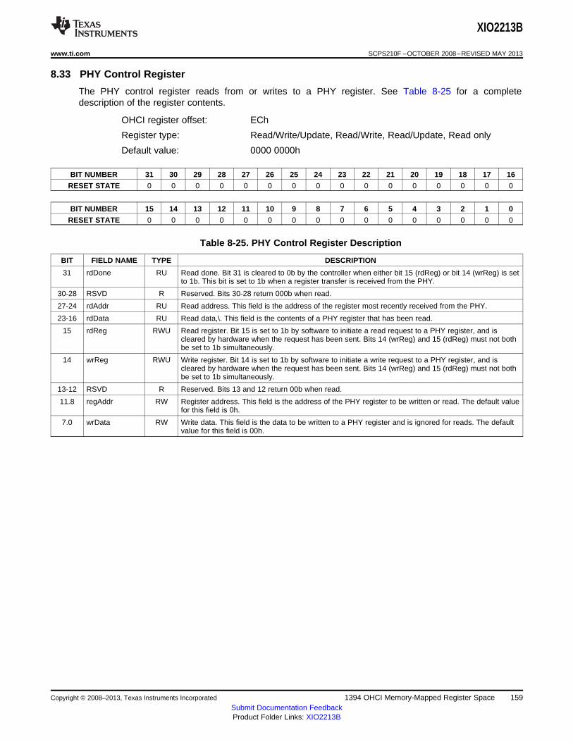
XIO2213B
www.ti.com SCPS210F –OCTOBER 2008–REVISED MAY 2013
8.33 PHY Control Register
The PHY control register reads from or writes to a PHY register. See Table 8-25 for a completedescription of the register contents.
OHCI register offset: ECh
Register type: Read/Write/Update, Read/Write, Read/Update, Read only
Default value: 0000 0000h
BIT NUMBER 31 30 29 28 27 26 25 24 23 22 21 20 19 18 17 16
RESET STATE 0 0 0 0 0 0 0 0 0 0 0 0 0 0 0 0
BIT NUMBER 15 14 13 12 11 10 9 8 7 6 5 4 3 2 1 0
RESET STATE 0 0 0 0 0 0 0 0 0 0 0 0 0 0 0 0
Table 8-25. PHY Control Register Description
BIT FIELD NAME TYPE DESCRIPTION
31 rdDone RU Read done. Bit 31 is cleared to 0b by the controller when either bit 15 (rdReg) or bit 14 (wrReg) is setto 1b. This bit is set to 1b when a register transfer is received from the PHY.
30-28 RSVD R Reserved. Bits 30-28 return 000b when read.
27-24 rdAddr RU Read address. This field is the address of the register most recently received from the PHY.
23-16 rdData RU Read data,\. This field is the contents of a PHY register that has been read.
15 rdReg RWU Read register. Bit 15 is set to 1b by software to initiate a read request to a PHY register, and iscleared by hardware when the request has been sent. Bits 14 (wrReg) and 15 (rdReg) must not bothbe set to 1b simultaneously.
14 wrReg RWU Write register. Bit 14 is set to 1b by software to initiate a write request to a PHY register, and iscleared by hardware when the request has been sent. Bits 14 (wrReg) and 15 (rdReg) must not bothbe set to 1b simultaneously.
13-12 RSVD R Reserved. Bits 13 and 12 return 00b when read.
11.8 regAddr RW Register address. This field is the address of the PHY register to be written or read. The default valuefor this field is 0h.
7.0 wrData RW Write data. This field is the data to be written to a PHY register and is ignored for reads. The defaultvalue for this field is 00h.
Copyright © 2008–2013, Texas Instruments Incorporated 1394 OHCI Memory-Mapped Register Space 159Submit Documentation FeedbackProduct Folder Links: XIO2213B
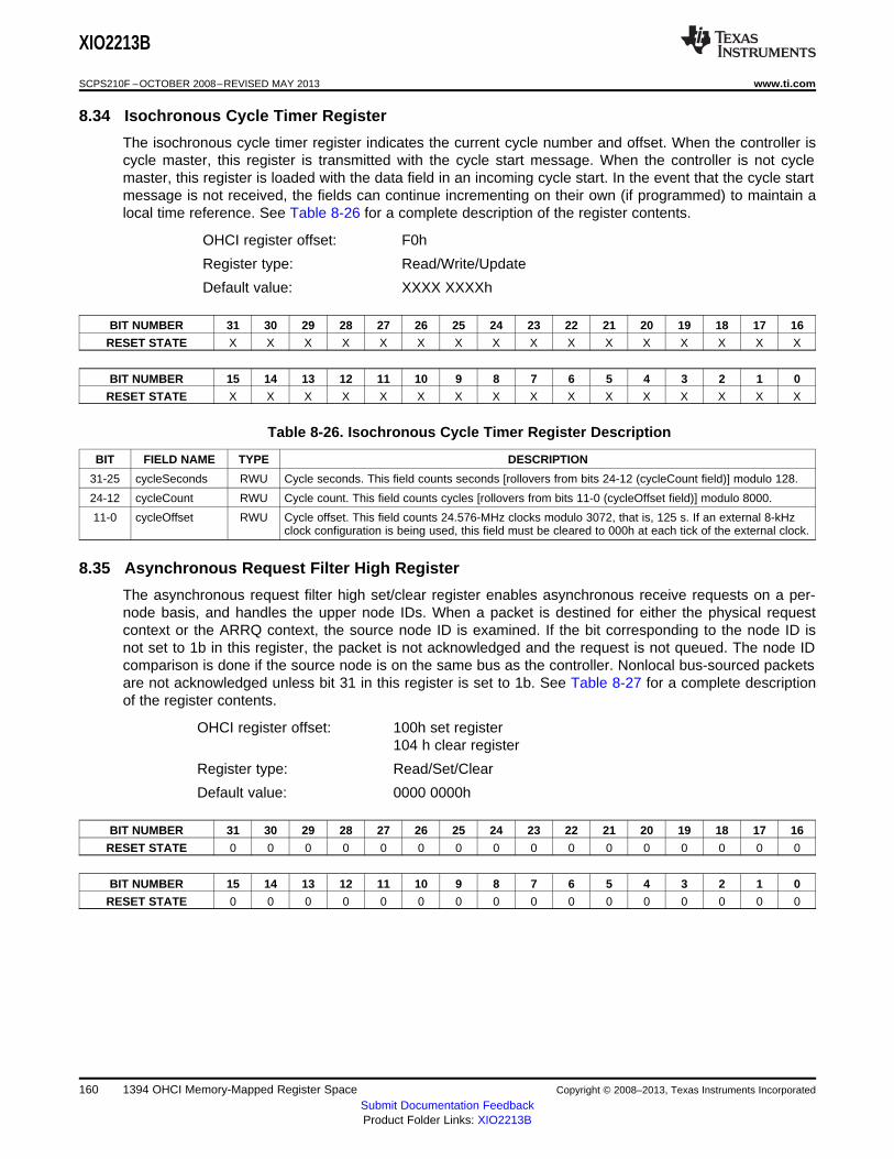
XIO2213B
SCPS210F –OCTOBER 2008–REVISED MAY 2013 www.ti.com
8.34 Isochronous Cycle Timer Register
The isochronous cycle timer register indicates the current cycle number and offset. When the controller iscycle master, this register is transmitted with the cycle start message. When the controller is not cyclemaster, this register is loaded with the data field in an incoming cycle start. In the event that the cycle startmessage is not received, the fields can continue incrementing on their own (if programmed) to maintain alocal time reference. See Table 8-26 for a complete description of the register contents.
OHCI register offset: F0h
Register type: Read/Write/Update
Default value: XXXX XXXXh
BIT NUMBER 31 30 29 28 27 26 25 24 23 22 21 20 19 18 17 16
RESET STATE X X X X X X X X X X X X X X X X
BIT NUMBER 15 14 13 12 11 10 9 8 7 6 5 4 3 2 1 0
RESET STATE X X X X X X X X X X X X X X X X
Table 8-26. Isochronous Cycle Timer Register Description
BIT FIELD NAME TYPE DESCRIPTION
31-25 cycleSeconds RWU Cycle seconds. This field counts seconds [rollovers from bits 24-12 (cycleCount field)] modulo 128.
24-12 cycleCount RWU Cycle count. This field counts cycles [rollovers from bits 11-0 (cycleOffset field)] modulo 8000.
11-0 cycleOffset RWU Cycle offset. This field counts 24.576-MHz clocks modulo 3072, that is, 125 s. If an external 8-kHzclock configuration is being used, this field must be cleared to 000h at each tick of the external clock.
8.35 Asynchronous Request Filter High Register
The asynchronous request filter high set/clear register enables asynchronous receive requests on a per-node basis, and handles the upper node IDs. When a packet is destined for either the physical requestcontext or the ARRQ context, the source node ID is examined. If the bit corresponding to the node ID isnot set to 1b in this register, the packet is not acknowledged and the request is not queued. The node IDcomparison is done if the source node is on the same bus as the controller. Nonlocal bus-sourced packetsare not acknowledged unless bit 31 in this register is set to 1b. See Table 8-27 for a complete descriptionof the register contents.
OHCI register offset: 100h set register104 h clear register
Register type: Read/Set/Clear
Default value: 0000 0000h
BIT NUMBER 31 30 29 28 27 26 25 24 23 22 21 20 19 18 17 16
RESET STATE 0 0 0 0 0 0 0 0 0 0 0 0 0 0 0 0
BIT NUMBER 15 14 13 12 11 10 9 8 7 6 5 4 3 2 1 0
RESET STATE 0 0 0 0 0 0 0 0 0 0 0 0 0 0 0 0
160 1394 OHCI Memory-Mapped Register Space Copyright © 2008–2013, Texas Instruments Incorporated
Submit Documentation FeedbackProduct Folder Links: XIO2213B
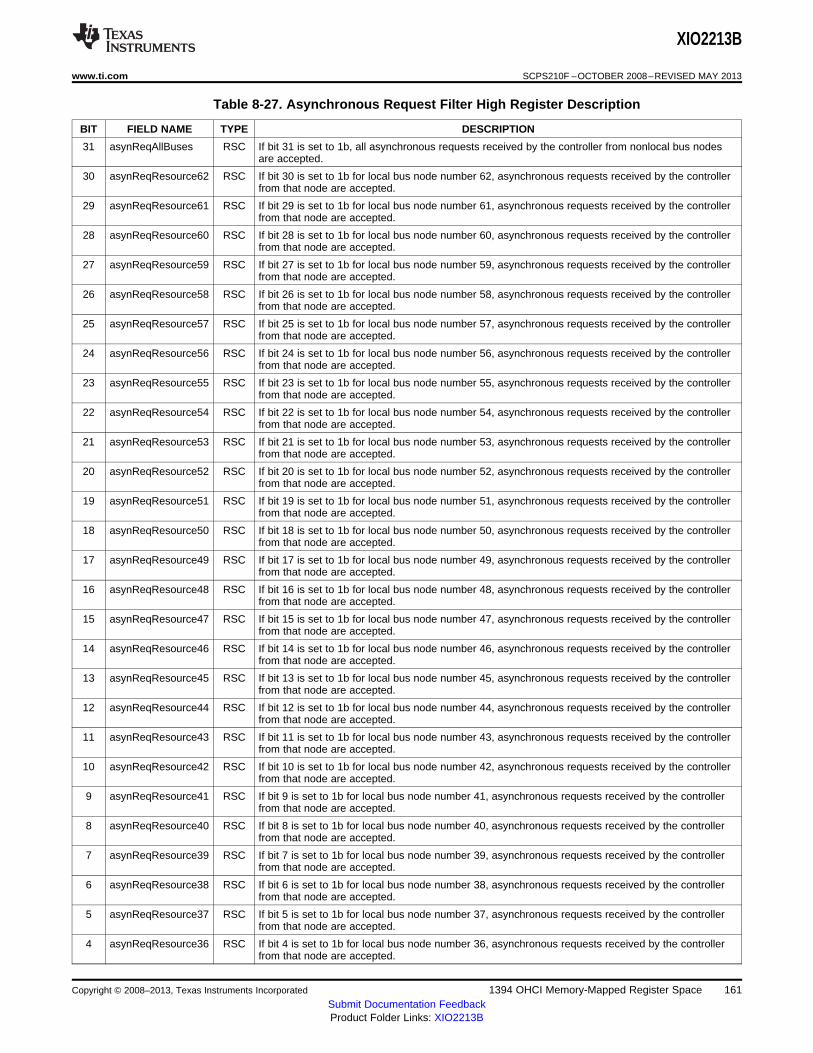
XIO2213B
www.ti.com SCPS210F –OCTOBER 2008–REVISED MAY 2013
Table 8-27. Asynchronous Request Filter High Register Description
BIT FIELD NAME TYPE DESCRIPTION
31 asynReqAllBuses RSC If bit 31 is set to 1b, all asynchronous requests received by the controller from nonlocal bus nodesare accepted.
30 asynReqResource62 RSC If bit 30 is set to 1b for local bus node number 62, asynchronous requests received by the controllerfrom that node are accepted.
29 asynReqResource61 RSC If bit 29 is set to 1b for local bus node number 61, asynchronous requests received by the controllerfrom that node are accepted.
28 asynReqResource60 RSC If bit 28 is set to 1b for local bus node number 60, asynchronous requests received by the controllerfrom that node are accepted.
27 asynReqResource59 RSC If bit 27 is set to 1b for local bus node number 59, asynchronous requests received by the controllerfrom that node are accepted.
26 asynReqResource58 RSC If bit 26 is set to 1b for local bus node number 58, asynchronous requests received by the controllerfrom that node are accepted.
25 asynReqResource57 RSC If bit 25 is set to 1b for local bus node number 57, asynchronous requests received by the controllerfrom that node are accepted.
24 asynReqResource56 RSC If bit 24 is set to 1b for local bus node number 56, asynchronous requests received by the controllerfrom that node are accepted.
23 asynReqResource55 RSC If bit 23 is set to 1b for local bus node number 55, asynchronous requests received by the controllerfrom that node are accepted.
22 asynReqResource54 RSC If bit 22 is set to 1b for local bus node number 54, asynchronous requests received by the controllerfrom that node are accepted.
21 asynReqResource53 RSC If bit 21 is set to 1b for local bus node number 53, asynchronous requests received by the controllerfrom that node are accepted.
20 asynReqResource52 RSC If bit 20 is set to 1b for local bus node number 52, asynchronous requests received by the controllerfrom that node are accepted.
19 asynReqResource51 RSC If bit 19 is set to 1b for local bus node number 51, asynchronous requests received by the controllerfrom that node are accepted.
18 asynReqResource50 RSC If bit 18 is set to 1b for local bus node number 50, asynchronous requests received by the controllerfrom that node are accepted.
17 asynReqResource49 RSC If bit 17 is set to 1b for local bus node number 49, asynchronous requests received by the controllerfrom that node are accepted.
16 asynReqResource48 RSC If bit 16 is set to 1b for local bus node number 48, asynchronous requests received by the controllerfrom that node are accepted.
15 asynReqResource47 RSC If bit 15 is set to 1b for local bus node number 47, asynchronous requests received by the controllerfrom that node are accepted.
14 asynReqResource46 RSC If bit 14 is set to 1b for local bus node number 46, asynchronous requests received by the controllerfrom that node are accepted.
13 asynReqResource45 RSC If bit 13 is set to 1b for local bus node number 45, asynchronous requests received by the controllerfrom that node are accepted.
12 asynReqResource44 RSC If bit 12 is set to 1b for local bus node number 44, asynchronous requests received by the controllerfrom that node are accepted.
11 asynReqResource43 RSC If bit 11 is set to 1b for local bus node number 43, asynchronous requests received by the controllerfrom that node are accepted.
10 asynReqResource42 RSC If bit 10 is set to 1b for local bus node number 42, asynchronous requests received by the controllerfrom that node are accepted.
9 asynReqResource41 RSC If bit 9 is set to 1b for local bus node number 41, asynchronous requests received by the controllerfrom that node are accepted.
8 asynReqResource40 RSC If bit 8 is set to 1b for local bus node number 40, asynchronous requests received by the controllerfrom that node are accepted.
7 asynReqResource39 RSC If bit 7 is set to 1b for local bus node number 39, asynchronous requests received by the controllerfrom that node are accepted.
6 asynReqResource38 RSC If bit 6 is set to 1b for local bus node number 38, asynchronous requests received by the controllerfrom that node are accepted.
5 asynReqResource37 RSC If bit 5 is set to 1b for local bus node number 37, asynchronous requests received by the controllerfrom that node are accepted.
4 asynReqResource36 RSC If bit 4 is set to 1b for local bus node number 36, asynchronous requests received by the controllerfrom that node are accepted.
Copyright © 2008–2013, Texas Instruments Incorporated 1394 OHCI Memory-Mapped Register Space 161Submit Documentation FeedbackProduct Folder Links: XIO2213B
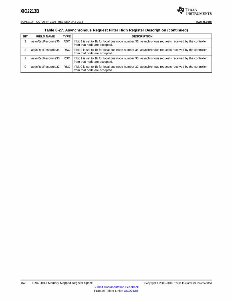
XIO2213B
SCPS210F –OCTOBER 2008–REVISED MAY 2013 www.ti.com
Table 8-27. Asynchronous Request Filter High Register Description (continued)
BIT FIELD NAME TYPE DESCRIPTION
3 asynReqResource35 RSC If bit 3 is set to 1b for local bus node number 35, asynchronous requests received by the controllerfrom that node are accepted.
2 asynReqResource34 RSC If bit 2 is set to 1b for local bus node number 34, asynchronous requests received by the controllerfrom that node are accepted.
1 asynReqResource33 RSC If bit 1 is set to 1b for local bus node number 33, asynchronous requests received by the controllerfrom that node are accepted.
0 asynReqResource32 RSC If bit 0 is set to 1b for local bus node number 32, asynchronous requests received by the controllerfrom that node are accepted.
162 1394 OHCI Memory-Mapped Register Space Copyright © 2008–2013, Texas Instruments Incorporated
Submit Documentation FeedbackProduct Folder Links: XIO2213B
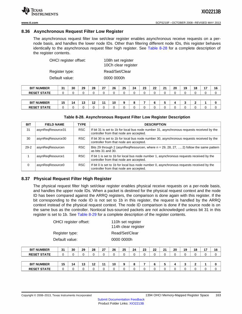
XIO2213B
www.ti.com SCPS210F –OCTOBER 2008–REVISED MAY 2013
8.36 Asynchronous Request Filter Low Register
The asynchronous request filter low set/clear register enables asynchronous receive requests on a per-node basis, and handles the lower node IDs. Other than filtering different node IDs, this register behavesidentically to the asynchronous request filter high register. See Table 8-28 for a complete description ofthe register contents.
OHCI register offset: 108h set register10Ch clear register
Register type: Read/Set/Clear
Default value: 0000 0000h
BIT NUMBER 31 30 29 28 27 26 25 24 23 22 21 20 19 18 17 16
RESET STATE 0 0 0 0 0 0 0 0 0 0 0 0 0 0 0 0
BIT NUMBER 15 14 13 12 11 10 9 8 7 6 5 4 3 2 1 0
RESET STATE 0 0 0 0 0 0 0 0 0 0 0 0 0 0 0 0
Table 8-28. Asynchronous Request Filter Low Register Description
BIT FIELD NAME TYPE DESCRIPTION
31 asynReqResource31 RSC If bit 31 is set to 1b for local bus node number 31, asynchronous requests received by thecontroller from that node are accepted.
30 asynReqResource30 RSC If bit 30 is set to 1b for local bus node number 30, asynchronous requests received by thecontroller from that node are accepted.
29-2 asynReqResourcen RSC Bits 29 through 2 (asynReqResourcen, where n = 29, 28, 27, ..., 2) follow the same patternas bits 31 and 30.
1 asynReqResource1 RSC If bit 1 is set to 1b for local bus node number 1, asynchronous requests received by thecontroller from that node are accepted.
0 asynReqResource0 RSC If bit 0 is set to 1b for local bus node number 0, asynchronous requests received by thecontroller from that node are accepted.
8.37 Physical Request Filter High Register
The physical request filter high set/clear register enables physical receive requests on a per-node basis,and handles the upper node IDs. When a packet is destined for the physical request context and the nodeID has been compared against the ARRQ registers, the comparison is done again with this register. If thebit corresponding to the node ID is not set to 1b in this register, the request is handled by the ARRQcontext instead of the physical request context. The node ID comparison is done if the source node is onthe same bus as the controller. Nonlocal bus-sourced packets are not acknowledged unless bit 31 in thisregister is set to 1b. See Table 8-29 for a complete description of the register contents.
OHCI register offset: 110h set register114h clear register
Register type: Read/Set/Clear
Default value: 0000 0000h
BIT NUMBER 31 30 29 28 27 26 25 24 23 22 21 20 19 18 17 16
RESET STATE 0 0 0 0 0 0 0 0 0 0 0 0 0 0 0 0
BIT NUMBER 15 14 13 12 11 10 9 8 7 6 5 4 3 2 1 0
RESET STATE 0 0 0 0 0 0 0 0 0 0 0 0 0 0 0 0
Copyright © 2008–2013, Texas Instruments Incorporated 1394 OHCI Memory-Mapped Register Space 163Submit Documentation FeedbackProduct Folder Links: XIO2213B
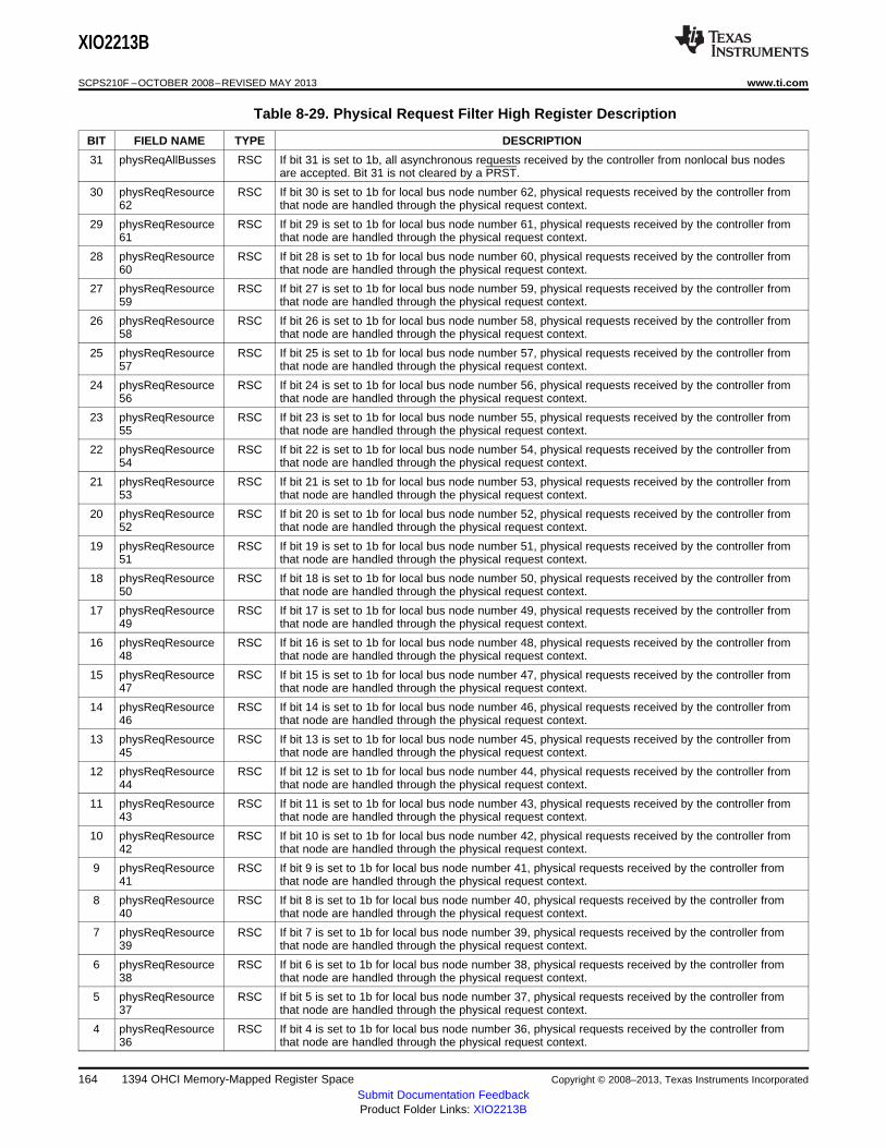
XIO2213B
SCPS210F –OCTOBER 2008–REVISED MAY 2013 www.ti.com
Table 8-29. Physical Request Filter High Register Description
BIT FIELD NAME TYPE DESCRIPTION
31 physReqAllBusses RSC If bit 31 is set to 1b, all asynchronous requests received by the controller from nonlocal bus nodesare accepted. Bit 31 is not cleared by a PRST.
30 physReqResource RSC If bit 30 is set to 1b for local bus node number 62, physical requests received by the controller from62 that node are handled through the physical request context.
29 physReqResource RSC If bit 29 is set to 1b for local bus node number 61, physical requests received by the controller from61 that node are handled through the physical request context.
28 physReqResource RSC If bit 28 is set to 1b for local bus node number 60, physical requests received by the controller from60 that node are handled through the physical request context.
27 physReqResource RSC If bit 27 is set to 1b for local bus node number 59, physical requests received by the controller from59 that node are handled through the physical request context.
26 physReqResource RSC If bit 26 is set to 1b for local bus node number 58, physical requests received by the controller from58 that node are handled through the physical request context.
25 physReqResource RSC If bit 25 is set to 1b for local bus node number 57, physical requests received by the controller from57 that node are handled through the physical request context.
24 physReqResource RSC If bit 24 is set to 1b for local bus node number 56, physical requests received by the controller from56 that node are handled through the physical request context.
23 physReqResource RSC If bit 23 is set to 1b for local bus node number 55, physical requests received by the controller from55 that node are handled through the physical request context.
22 physReqResource RSC If bit 22 is set to 1b for local bus node number 54, physical requests received by the controller from54 that node are handled through the physical request context.
21 physReqResource RSC If bit 21 is set to 1b for local bus node number 53, physical requests received by the controller from53 that node are handled through the physical request context.
20 physReqResource RSC If bit 20 is set to 1b for local bus node number 52, physical requests received by the controller from52 that node are handled through the physical request context.
19 physReqResource RSC If bit 19 is set to 1b for local bus node number 51, physical requests received by the controller from51 that node are handled through the physical request context.
18 physReqResource RSC If bit 18 is set to 1b for local bus node number 50, physical requests received by the controller from50 that node are handled through the physical request context.
17 physReqResource RSC If bit 17 is set to 1b for local bus node number 49, physical requests received by the controller from49 that node are handled through the physical request context.
16 physReqResource RSC If bit 16 is set to 1b for local bus node number 48, physical requests received by the controller from48 that node are handled through the physical request context.
15 physReqResource RSC If bit 15 is set to 1b for local bus node number 47, physical requests received by the controller from47 that node are handled through the physical request context.
14 physReqResource RSC If bit 14 is set to 1b for local bus node number 46, physical requests received by the controller from46 that node are handled through the physical request context.
13 physReqResource RSC If bit 13 is set to 1b for local bus node number 45, physical requests received by the controller from45 that node are handled through the physical request context.
12 physReqResource RSC If bit 12 is set to 1b for local bus node number 44, physical requests received by the controller from44 that node are handled through the physical request context.
11 physReqResource RSC If bit 11 is set to 1b for local bus node number 43, physical requests received by the controller from43 that node are handled through the physical request context.
10 physReqResource RSC If bit 10 is set to 1b for local bus node number 42, physical requests received by the controller from42 that node are handled through the physical request context.
9 physReqResource RSC If bit 9 is set to 1b for local bus node number 41, physical requests received by the controller from41 that node are handled through the physical request context.
8 physReqResource RSC If bit 8 is set to 1b for local bus node number 40, physical requests received by the controller from40 that node are handled through the physical request context.
7 physReqResource RSC If bit 7 is set to 1b for local bus node number 39, physical requests received by the controller from39 that node are handled through the physical request context.
6 physReqResource RSC If bit 6 is set to 1b for local bus node number 38, physical requests received by the controller from38 that node are handled through the physical request context.
5 physReqResource RSC If bit 5 is set to 1b for local bus node number 37, physical requests received by the controller from37 that node are handled through the physical request context.
4 physReqResource RSC If bit 4 is set to 1b for local bus node number 36, physical requests received by the controller from36 that node are handled through the physical request context.
164 1394 OHCI Memory-Mapped Register Space Copyright © 2008–2013, Texas Instruments Incorporated
Submit Documentation FeedbackProduct Folder Links: XIO2213B
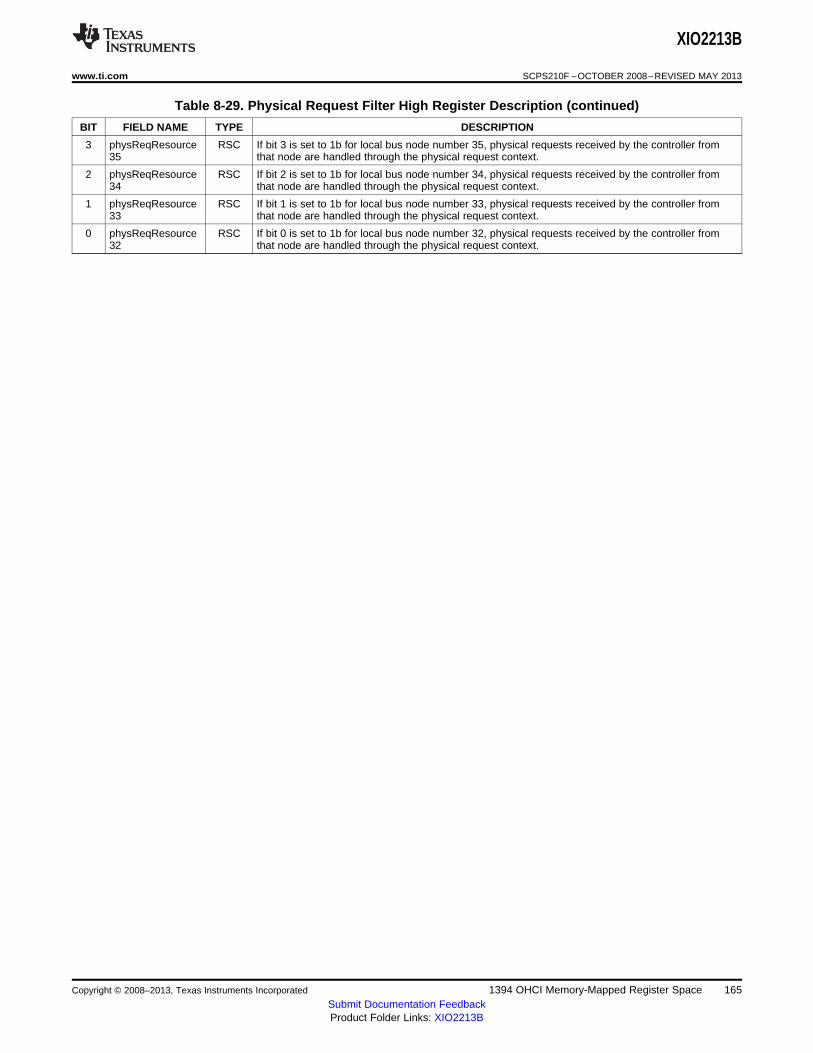
XIO2213B
www.ti.com SCPS210F –OCTOBER 2008–REVISED MAY 2013
Table 8-29. Physical Request Filter High Register Description (continued)
BIT FIELD NAME TYPE DESCRIPTION
3 physReqResource RSC If bit 3 is set to 1b for local bus node number 35, physical requests received by the controller from35 that node are handled through the physical request context.
2 physReqResource RSC If bit 2 is set to 1b for local bus node number 34, physical requests received by the controller from34 that node are handled through the physical request context.
1 physReqResource RSC If bit 1 is set to 1b for local bus node number 33, physical requests received by the controller from33 that node are handled through the physical request context.
0 physReqResource RSC If bit 0 is set to 1b for local bus node number 32, physical requests received by the controller from32 that node are handled through the physical request context.
Copyright © 2008–2013, Texas Instruments Incorporated 1394 OHCI Memory-Mapped Register Space 165Submit Documentation FeedbackProduct Folder Links: XIO2213B
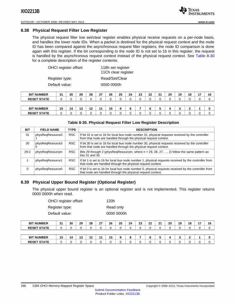
XIO2213B
SCPS210F –OCTOBER 2008–REVISED MAY 2013 www.ti.com
8.38 Physical Request Filter Low Register
The physical request filter low set/clear register enables physical receive requests on a per-node basis,and handles the lower node IDs. When a packet is destined for the physical request context and the nodeID has been compared against the asynchronous request filter registers, the node ID comparison is doneagain with this register. If the bit corresponding to the node ID is not set to 1b in this register, the requestis handled by the asynchronous request context instead of the physical request context. See Table 8-30for a complete description of the register contents.
OHCI register offset: 118h set register11Ch clear register
Register type: Read/Set/Clear
Default value: 0000 0000h
BIT NUMBER 31 30 29 28 27 26 25 24 23 22 21 20 19 18 17 16
RESET STATE 0 0 0 0 0 0 0 0 0 0 0 0 0 0 0 0
BIT NUMBER 15 14 13 12 11 10 9 8 7 6 5 4 3 2 1 0
RESET STATE 0 0 0 0 0 0 0 0 0 0 0 0 0 0 0 0
Table 8-30. Physical Request Filter Low Register Description
BIT FIELD NAME TYPE DESCRIPTION
31 physReqResource3 RSC If bit 31 is set to 1b for local bus node number 31, physical requests received by the controller1 from that node are handled through the physical request context.
30 physReqResource3 RSC If bit 30 is set to 1b for local bus node number 30, physical requests received by the controller0 from that node are handled through the physical request context.
29-2 physReqResourcen RSC Bits 29 through 2 (physReqResourcen, where n = 29, 28, 27, ..., 2) follow the same pattern asbits 31 and 30.
1 physReqResource1 RSC If bit 1 is set to 1b for local bus node number 1, physical requests received by the controller fromthat node are handled through the physical request context.
0 physReqResource0 RSC If bit 0 is set to 1b for local bus node number 0, physical requests received by the controller fromthat node are handled through the physical request context.
8.39 Physical Upper Bound Register (Optional Register)
The physical upper bound register is an optional register and is not implemented. This register returns0000 0000h when read.
OHCI register offset: 120h
Register type: Read only
Default value: 0000 0000h
BIT NUMBER 31 30 29 28 27 26 25 24 23 22 21 20 19 18 17 16
RESET STATE 0 0 0 0 0 0 0 0 0 0 0 0 0 0 0 0
BIT NUMBER 15 14 13 12 11 10 9 8 7 6 5 4 3 2 1 0
RESET STATE 0 0 0 0 0 0 0 0 0 0 0 0 0 0 0 0
166 1394 OHCI Memory-Mapped Register Space Copyright © 2008–2013, Texas Instruments Incorporated
Submit Documentation FeedbackProduct Folder Links: XIO2213B
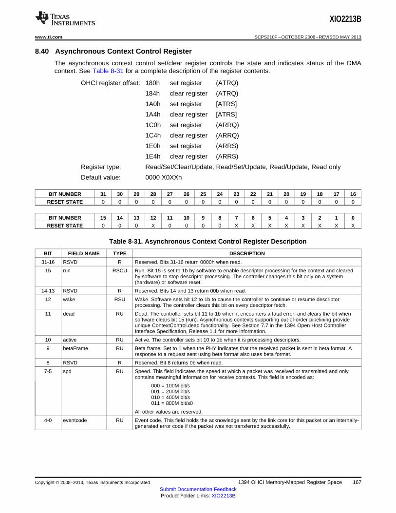
XIO2213B
www.ti.com SCPS210F –OCTOBER 2008–REVISED MAY 2013
8.40 Asynchronous Context Control Register
The asynchronous context control set/clear register controls the state and indicates status of the DMAcontext. See Table 8-31 for a complete description of the register contents.
OHCI register offset: 180h set register (ATRQ)
184h clear register (ATRQ)
1A0h set register [ATRS]
1A4h clear register [ATRS]
1C0h set register (ARRQ)
1C4h clear register (ARRQ)
1E0h set register (ARRS)
1E4h clear register (ARRS)
Register type: Read/Set/Clear/Update, Read/Set/Update, Read/Update, Read only
Default value: 0000 X0XXh
BIT NUMBER 31 30 29 28 27 26 25 24 23 22 21 20 19 18 17 16
RESET STATE 0 0 0 0 0 0 0 0 0 0 0 0 0 0 0 0
BIT NUMBER 15 14 13 12 11 10 9 8 7 6 5 4 3 2 1 0
RESET STATE 0 0 0 X 0 0 0 0 X X X X X X X X
Table 8-31. Asynchronous Context Control Register Description
BIT FIELD NAME TYPE DESCRIPTION
31-16 RSVD R Reserved. Bits 31-16 return 0000h when read.
15 run RSCU Run. Bit 15 is set to 1b by software to enable descriptor processing for the context and clearedby software to stop descriptor processing. The controller changes this bit only on a system(hardware) or software reset.
14-13 RSVD R Reserved. Bits 14 and 13 return 00b when read.
12 wake RSU Wake. Software sets bit 12 to 1b to cause the controller to continue or resume descriptorprocessing. The controller clears this bit on every descriptor fetch.
11 dead RU Dead. The controller sets bit 11 to 1b when it encounters a fatal error, and clears the bit whensoftware clears bit 15 (run). Asynchronous contexts supporting out-of-order pipelining provideunique ContextControl.dead functionality. See Section 7.7 in the 1394 Open Host ControllerInterface Specification, Release 1.1 for more information.
10 active RU Active. The controller sets bit 10 to 1b when it is processing descriptors.
9 betaFrame RU Beta frame. Set to 1 when the PHY indicates that the received packet is sent in beta format. Aresponse to a request sent using beta format also uses beta format.
8 RSVD R Reserved. Bit 8 returns 0b when read.
7-5 spd RU Speed. This field indicates the speed at which a packet was received or transmitted and onlycontains meaningful information for receive contexts. This field is encoded as:
000 = 100M bit/s001 = 200M bit/s010 = 400M bit/s011 = 800M bit/s0
All other values are reserved.
4-0 eventcode RU Event code. This field holds the acknowledge sent by the link core for this packet or an internally-generated error code if the packet was not transferred successfully.
Copyright © 2008–2013, Texas Instruments Incorporated 1394 OHCI Memory-Mapped Register Space 167Submit Documentation FeedbackProduct Folder Links: XIO2213B
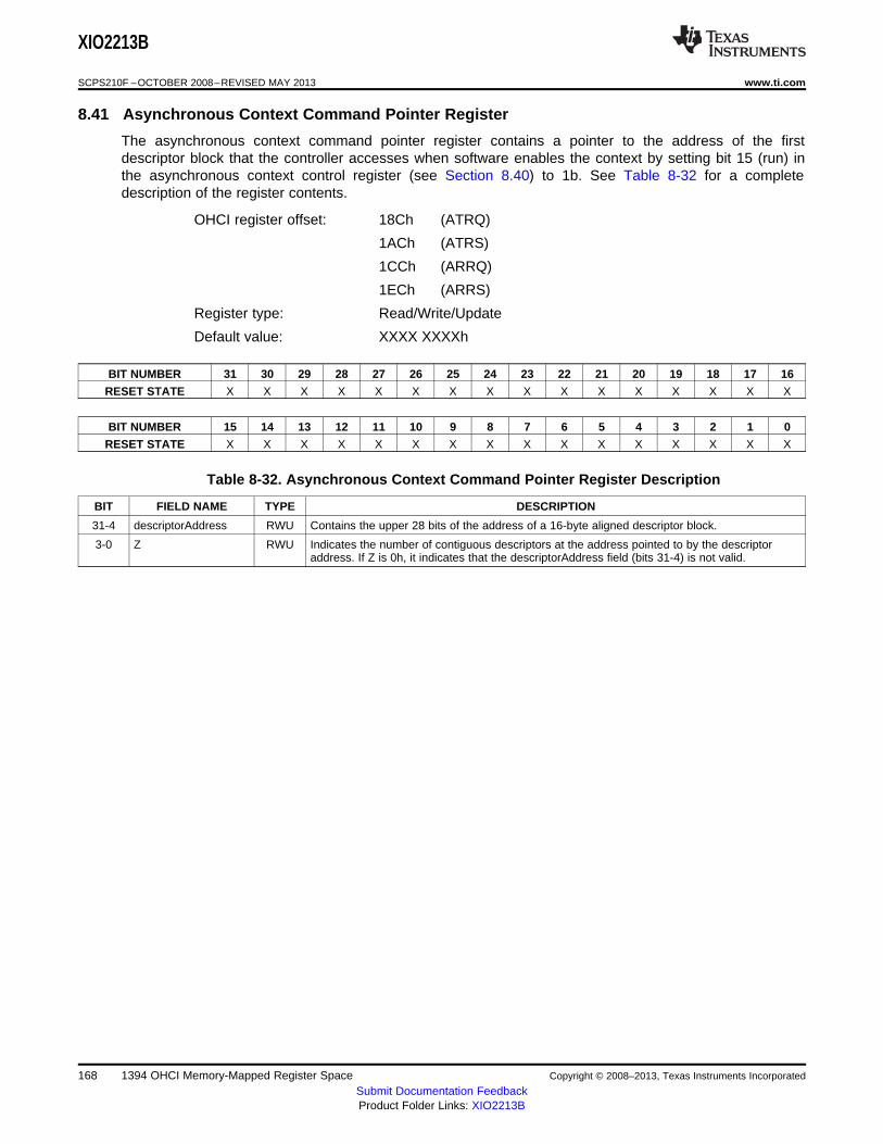
XIO2213B
SCPS210F –OCTOBER 2008–REVISED MAY 2013 www.ti.com
8.41 Asynchronous Context Command Pointer Register
The asynchronous context command pointer register contains a pointer to the address of the firstdescriptor block that the controller accesses when software enables the context by setting bit 15 (run) inthe asynchronous context control register (see Section 8.40) to 1b. See Table 8-32 for a completedescription of the register contents.
OHCI register offset: 18Ch (ATRQ)
1ACh (ATRS)
1CCh (ARRQ)
1ECh (ARRS)
Register type: Read/Write/Update
Default value: XXXX XXXXh
BIT NUMBER 31 30 29 28 27 26 25 24 23 22 21 20 19 18 17 16
RESET STATE X X X X X X X X X X X X X X X X
BIT NUMBER 15 14 13 12 11 10 9 8 7 6 5 4 3 2 1 0
RESET STATE X X X X X X X X X X X X X X X X
Table 8-32. Asynchronous Context Command Pointer Register Description
BIT FIELD NAME TYPE DESCRIPTION
31-4 descriptorAddress RWU Contains the upper 28 bits of the address of a 16-byte aligned descriptor block.
3-0 Z RWU Indicates the number of contiguous descriptors at the address pointed to by the descriptoraddress. If Z is 0h, it indicates that the descriptorAddress field (bits 31-4) is not valid.
168 1394 OHCI Memory-Mapped Register Space Copyright © 2008–2013, Texas Instruments Incorporated
Submit Documentation FeedbackProduct Folder Links: XIO2213B
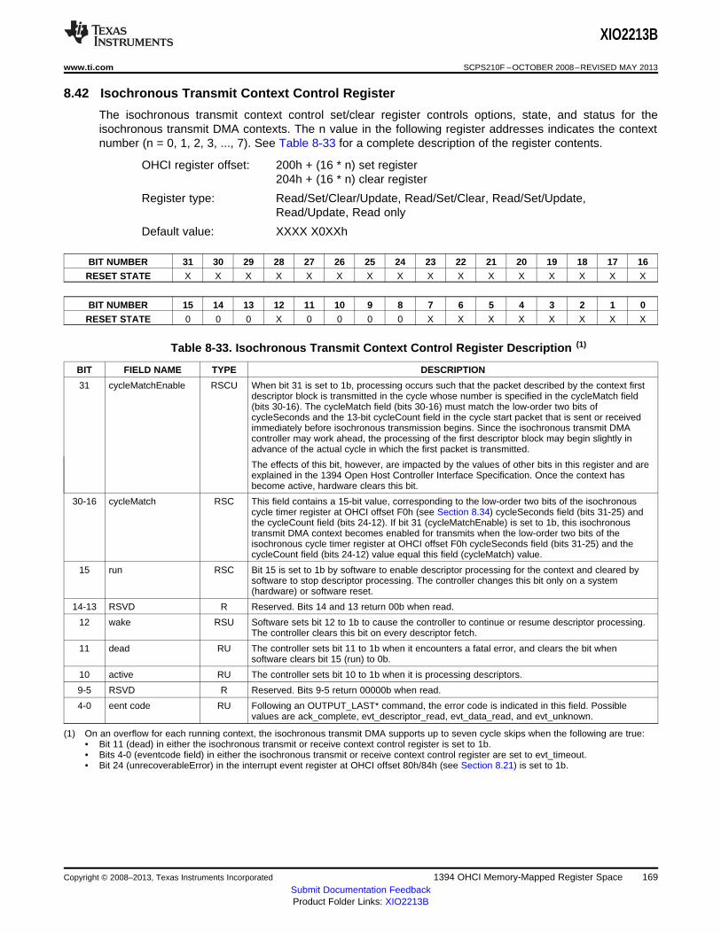
XIO2213B
www.ti.com SCPS210F –OCTOBER 2008–REVISED MAY 2013
8.42 Isochronous Transmit Context Control Register
The isochronous transmit context control set/clear register controls options, state, and status for theisochronous transmit DMA contexts. The n value in the following register addresses indicates the contextnumber (n = 0, 1, 2, 3, ..., 7). See Table 8-33 for a complete description of the register contents.
OHCI register offset: 200h + (16 * n) set register204h + (16 * n) clear register
Register type: Read/Set/Clear/Update, Read/Set/Clear, Read/Set/Update,Read/Update, Read only
Default value: XXXX X0XXh
BIT NUMBER 31 30 29 28 27 26 25 24 23 22 21 20 19 18 17 16
RESET STATE X X X X X X X X X X X X X X X X
BIT NUMBER 15 14 13 12 11 10 9 8 7 6 5 4 3 2 1 0
RESET STATE 0 0 0 X 0 0 0 0 X X X X X X X X
Table 8-33. Isochronous Transmit Context Control Register Description (1)
BIT FIELD NAME TYPE DESCRIPTION
31 cycleMatchEnable RSCU When bit 31 is set to 1b, processing occurs such that the packet described by the context firstdescriptor block is transmitted in the cycle whose number is specified in the cycleMatch field(bits 30-16). The cycleMatch field (bits 30-16) must match the low-order two bits ofcycleSeconds and the 13-bit cycleCount field in the cycle start packet that is sent or receivedimmediately before isochronous transmission begins. Since the isochronous transmit DMAcontroller may work ahead, the processing of the first descriptor block may begin slightly inadvance of the actual cycle in which the first packet is transmitted.
The effects of this bit, however, are impacted by the values of other bits in this register and areexplained in the 1394 Open Host Controller Interface Specification. Once the context hasbecome active, hardware clears this bit.
30-16 cycleMatch RSC This field contains a 15-bit value, corresponding to the low-order two bits of the isochronouscycle timer register at OHCI offset F0h (see Section 8.34) cycleSeconds field (bits 31-25) andthe cycleCount field (bits 24-12). If bit 31 (cycleMatchEnable) is set to 1b, this isochronoustransmit DMA context becomes enabled for transmits when the low-order two bits of theisochronous cycle timer register at OHCI offset F0h cycleSeconds field (bits 31-25) and thecycleCount field (bits 24-12) value equal this field (cycleMatch) value.
15 run RSC Bit 15 is set to 1b by software to enable descriptor processing for the context and cleared bysoftware to stop descriptor processing. The controller changes this bit only on a system(hardware) or software reset.
14-13 RSVD R Reserved. Bits 14 and 13 return 00b when read.
12 wake RSU Software sets bit 12 to 1b to cause the controller to continue or resume descriptor processing.The controller clears this bit on every descriptor fetch.
11 dead RU The controller sets bit 11 to 1b when it encounters a fatal error, and clears the bit whensoftware clears bit 15 (run) to 0b.
10 active RU The controller sets bit 10 to 1b when it is processing descriptors.
9-5 RSVD R Reserved. Bits 9-5 return 00000b when read.
4-0 eent code RU Following an OUTPUT_LAST* command, the error code is indicated in this field. Possiblevalues are ack_complete, evt_descriptor_read, evt_data_read, and evt_unknown.
(1) On an overflow for each running context, the isochronous transmit DMA supports up to seven cycle skips when the following are true:• Bit 11 (dead) in either the isochronous transmit or receive context control register is set to 1b.• Bits 4-0 (eventcode field) in either the isochronous transmit or receive context control register are set to evt_timeout.• Bit 24 (unrecoverableError) in the interrupt event register at OHCI offset 80h/84h (see Section 8.21) is set to 1b.
Copyright © 2008–2013, Texas Instruments Incorporated 1394 OHCI Memory-Mapped Register Space 169Submit Documentation FeedbackProduct Folder Links: XIO2213B
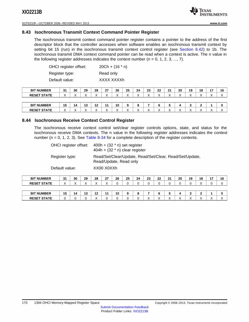
XIO2213B
SCPS210F –OCTOBER 2008–REVISED MAY 2013 www.ti.com
8.43 Isochronous Transmit Context Command Pointer Register
The isochronous transmit context command pointer register contains a pointer to the address of the firstdescriptor block that the controller accesses when software enables an isochronous transmit context bysetting bit 15 (run) in the isochronous transmit context control register (see Section 8.42) to 1b. Theisochronous transmit DMA context command pointer can be read when a context is active. The n value inthe following register addresses indicates the context number (n = 0, 1, 2, 3, ..., 7).
OHCI register offset: 20Ch + (16 * n)
Register type: Read only
Default value: XXXX XXXXh
BIT NUMBER 31 30 29 28 27 26 25 24 23 22 21 20 19 18 17 16
RESET STATE X X X X X X X X X X X X X X X X
BIT NUMBER 15 14 13 12 11 10 9 8 7 6 5 4 3 2 1 0
RESET STATE X X X X X X X X X X X X X X X X
8.44 Isochronous Receive Context Control Register
The isochronous receive context control set/clear register controls options, state, and status for theisochronous receive DMA contexts. The n value in the following register addresses indicates the contextnumber (n = 0, 1, 2, 3). See Table 8-34 for a complete description of the register contents.
OHCI register offset: 400h + (32 * n) set register404h + (32 * n) clear register
Register type: Read/Set/Clear/Update, Read/Set/Clear, Read/Set/Update,Read/Update, Read only
Default value: XX00 X0XXh
BIT NUMBER 31 30 29 28 27 26 25 24 23 22 21 20 19 18 17 16
RESET STATE X X X X X 0 0 0 0 0 0 0 0 0 0 0
BIT NUMBER 15 14 13 12 11 10 9 8 7 6 5 4 3 2 1 0
RESET STATE 0 0 0 X 0 0 0 0 X X X X X X X X
170 1394 OHCI Memory-Mapped Register Space Copyright © 2008–2013, Texas Instruments Incorporated
Submit Documentation FeedbackProduct Folder Links: XIO2213B
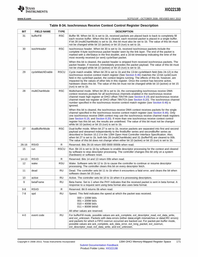
XIO2213B
www.ti.com SCPS210F –OCTOBER 2008–REVISED MAY 2013
Table 8-34. Isochronous Receive Context Control Register Description
BIT FIELD NAME TYPE DESCRIPTION
31 bufferFill RSC Buffer fill. When bit 31 is set to 1b, received packets are placed back to back to completely filleach receive buffer. When this bit is cleared, each received packet is placed in a single buffer.If bit 28 (multiChanMode) is set to 1b, this bit must also be set to 1b. The value of this bit mustnot be changed while bit 10 (active) or bit 15 (run) is set to 1b.
30 isochHeader RSC Isochronous header. When bit 30 is set to 1b, received isochronous packets include thecomplete 4-byte isochronous packet header seen by the link layer. The end of the packet ismarked with a xferStatus in the first doublet, and a 16-bit timestamp indicating the time of themost recently received (or sent) cycleStart packet.
When this bit is cleared, the packet header is stripped from received isochronous packets. Thepacket header, if received, immediately precedes the packet payload. The value of this bit mustnot be changed while bit 10 (active) or bit 15 (run) is set to 1b.
29 cycleMatchEnable RSCU Cycle match enable. When bit 29 is set to 1b and the 13-bit cycleMatch field (bits 24-12) in theisochronous receive context match register (See Section 8.46) matches the 13-bit cycleCountfield in the cycleStart packet, the context begins running. The effects of this bit, however, areimpacted by the values of other bits in this register. Once the context has become active,hardware clears this bit. The value of this bit must not be changed while bit 10 (active) or bit 15(run) is set to 1b.
28 multiChanMode RSC Multichannel mode. When bit 28 is set to 1b, the corresponding isochronous receive DMAcontext receives packets for all isochronous channels enabled in the isochronous receivechannel mask high register at OHCI offset 70h/74h (see Section 8.19) and isochronous receivechannel mask low register at OHCI offset 78h/7Ch (see Section 8.20). The isochronous channelnumber specified in the isochronous receive context match register (see Section 8.46) isignored.
When this bit is cleared, the isochronous receive DMA context receives packets for the singlechannel specified in the isochronous receive context match register (see Section 8.46). Onlyone isochronous receive DMA context may use the isochronous receive channel mask registers(see Section 8.19, and Section 8.20). If more than one isochronous receive context controlregister has this bit set, the results are undefined. The value of this bit must not be changedwhile bit 10 (active) or bit 15 (run) is set to 1b.
27 dualBufferMode RSC Dual-buffer mode. When bit 27 is set to 1b, receive packets are separated into first and secondpayload and streamed independently to the firstBuffer series and secondBuffer series asdescribed in Section 10.2.3 in the 1394 Open Host Controller Interface Specification. Also,when bit 27 is set to 1b, both bits 28 (multiChanMode) and 31 (bufferFill) are cleared to 00b.The value of this bit does not change when either bit 10 (active) or bit 15 (run) is set to 1b.
26-16 RSVD R Reserved. Bits 26-16 return 000 0000 0000b when read.
15 run RSCU Run. Bit 15 is set to 1b by software to enable descriptor processing for the context and clearedby software to stop descriptor processing. The controller changes this bit only on a system(hardware) or software reset.
14-13 RSVD R Reserved. Bits 14 and 13 return 00b when read.
12 wake RSU Wake. Software sets bit 12 to 1b to cause the controller to continue or resume descriptorprocessing. The controller clears this bit on every descriptor fetch.
11 dead RU Dead. The controller sets bit 11 to 1b when it encounters a fatal error, and clears the bit whensoftware clears bit 15 (run).
10 active RU Active. The controller sets bit 10 to 1b when it is processing descriptors.
9 betaFrame RU Beta frame. Set to 1 when the PHY indicates that the received packet is sent in beta format. Aresponse to a request sent using beta format also uses beta format.
9-8 RSVD R Reserved. Bit 8 returns 0b when read.
7-8 spd RU Speed. This field indicates the speed at which the packet was received.
000 = 100M bit/s001 = 200M bit/s010 = 400M bit/s011 = 800M bit/s0
All other values are reserved.
4-0 event code RU For bufferFill mode, possible values are ack_complete, evt_descriptor_read, evt_data_write,and evt_unknown. Packets with data errors (either dataLength mismatches or dataCRC errors)and packets for which a FIFO overrun occurred are backed out. For packet-per-buffer mode,possible values are ack_complete, ack_data_error, evt_long_packet, evt_overrun,evt_descriptor_read, evt_data_write, and evt_unknown.
Copyright © 2008–2013, Texas Instruments Incorporated 1394 OHCI Memory-Mapped Register Space 171Submit Documentation FeedbackProduct Folder Links: XIO2213B
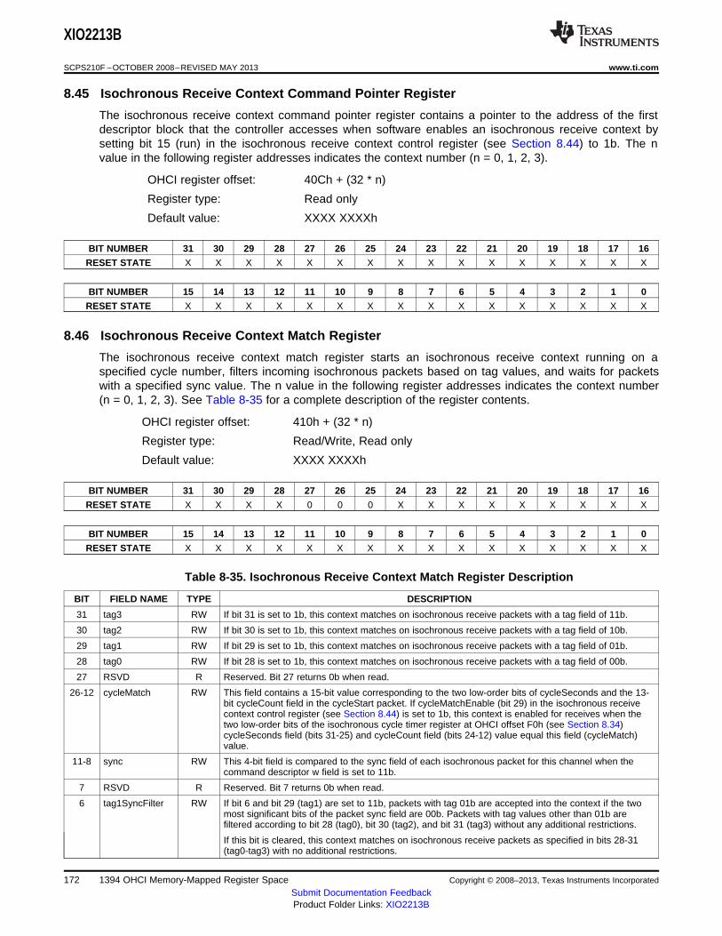
XIO2213B
SCPS210F –OCTOBER 2008–REVISED MAY 2013 www.ti.com
8.45 Isochronous Receive Context Command Pointer Register
The isochronous receive context command pointer register contains a pointer to the address of the firstdescriptor block that the controller accesses when software enables an isochronous receive context bysetting bit 15 (run) in the isochronous receive context control register (see Section 8.44) to 1b. The nvalue in the following register addresses indicates the context number (n = 0, 1, 2, 3).
OHCI register offset: 40Ch + (32 * n)
Register type: Read only
Default value: XXXX XXXXh
BIT NUMBER 31 30 29 28 27 26 25 24 23 22 21 20 19 18 17 16
RESET STATE X X X X X X X X X X X X X X X X
BIT NUMBER 15 14 13 12 11 10 9 8 7 6 5 4 3 2 1 0
RESET STATE X X X X X X X X X X X X X X X X
8.46 Isochronous Receive Context Match Register
The isochronous receive context match register starts an isochronous receive context running on aspecified cycle number, filters incoming isochronous packets based on tag values, and waits for packetswith a specified sync value. The n value in the following register addresses indicates the context number(n = 0, 1, 2, 3). See Table 8-35 for a complete description of the register contents.
OHCI register offset: 410h + (32 * n)
Register type: Read/Write, Read only
Default value: XXXX XXXXh
BIT NUMBER 31 30 29 28 27 26 25 24 23 22 21 20 19 18 17 16
RESET STATE X X X X 0 0 0 X X X X X X X X X
BIT NUMBER 15 14 13 12 11 10 9 8 7 6 5 4 3 2 1 0
RESET STATE X X X X X X X X X X X X X X X X
Table 8-35. Isochronous Receive Context Match Register Description
BIT FIELD NAME TYPE DESCRIPTION
31 tag3 RW If bit 31 is set to 1b, this context matches on isochronous receive packets with a tag field of 11b.
30 tag2 RW If bit 30 is set to 1b, this context matches on isochronous receive packets with a tag field of 10b.
29 tag1 RW If bit 29 is set to 1b, this context matches on isochronous receive packets with a tag field of 01b.
28 tag0 RW If bit 28 is set to 1b, this context matches on isochronous receive packets with a tag field of 00b.
27 RSVD R Reserved. Bit 27 returns 0b when read.
26-12 cycleMatch RW This field contains a 15-bit value corresponding to the two low-order bits of cycleSeconds and the 13-bit cycleCount field in the cycleStart packet. If cycleMatchEnable (bit 29) in the isochronous receivecontext control register (see Section 8.44) is set to 1b, this context is enabled for receives when thetwo low-order bits of the isochronous cycle timer register at OHCI offset F0h (see Section 8.34)cycleSeconds field (bits 31-25) and cycleCount field (bits 24-12) value equal this field (cycleMatch)value.
11-8 sync RW This 4-bit field is compared to the sync field of each isochronous packet for this channel when thecommand descriptor w field is set to 11b.
7 RSVD R Reserved. Bit 7 returns 0b when read.
6 tag1SyncFilter RW If bit 6 and bit 29 (tag1) are set to 11b, packets with tag 01b are accepted into the context if the twomost significant bits of the packet sync field are 00b. Packets with tag values other than 01b arefiltered according to bit 28 (tag0), bit 30 (tag2), and bit 31 (tag3) without any additional restrictions.
If this bit is cleared, this context matches on isochronous receive packets as specified in bits 28-31(tag0-tag3) with no additional restrictions.
172 1394 OHCI Memory-Mapped Register Space Copyright © 2008–2013, Texas Instruments Incorporated
Submit Documentation FeedbackProduct Folder Links: XIO2213B

XIO2213B
www.ti.com SCPS210F –OCTOBER 2008–REVISED MAY 2013
Table 8-35. Isochronous Receive Context Match Register Description (continued)
BIT FIELD NAME TYPE DESCRIPTION
5-0 channelNumber RW This 6-bit field indicates the isochronous channel number for which this isochronous receive DMAcontext accepts packets.
Copyright © 2008–2013, Texas Instruments Incorporated 1394 OHCI Memory-Mapped Register Space 173Submit Documentation FeedbackProduct Folder Links: XIO2213B
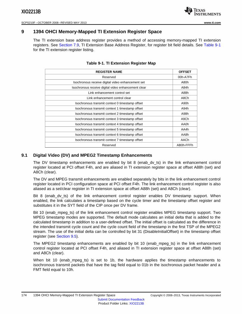
XIO2213B
SCPS210F –OCTOBER 2008–REVISED MAY 2013 www.ti.com
9 1394 OHCI Memory-Mapped TI Extension Register Space
The TI extension base address register provides a method of accessing memory-mapped TI extensionregisters. See Section 7.9, TI Extension Base Address Register, for register bit field details. See Table 9-1for the TI extension register listing.
Table 9-1. TI Extension Register Map
REGISTER NAME OFFSET
Reserved 00h-A7Fh
Isochronous receive digital video enhancement set A80h
Isochronous receive digital video enhancement clear A84h
Link enhancement control set A88h
Link enhancement control clear A8Ch
Isochronous transmit context 0 timestamp offset A90h
Isochronous transmit context 1 timestamp offset A94h
Isochronous transmit context 2 timestamp offset A98h
Isochronous transmit context 3 timestamp offset A9Ch
Isochronous transmit context 4 timestamp offset AA0h
Isochronous transmit context 5 timestamp offset AA4h
Isochronous transmit context 6 timestamp offset AA8h
Isochronous transmit context 7 timestamp offset AACh
Reserved AB0h-FFFh
9.1 Digital Video (DV) and MPEG2 Timestamp Enhancements
The DV timestamp enhancements are enabled by bit 8 (enab_dv_ts) in the link enhancement controlregister located at PCI offset F4h, and are aliased in TI extension register space at offset A88h (set) andA8Ch (clear).
The DV and MPEG transmit enhancements are enabled separately by bits in the link enhancement controlregister located in PCI configuration space at PCI offset F4h. The link enhancement control register is alsoaliased as a set/clear register in TI extension space at offset A88h (set) and A8Ch (clear).
Bit 8 (enab_dv_ts) of the link enhancement control register enables DV timestamp support. Whenenabled, the link calculates a timestamp based on the cycle timer and the timestamp offset register andsubstitutes it in the SYT field of the CIP once per DV frame.
Bit 10 (enab_mpeg_ts) of the link enhancement control register enables MPEG timestamp support. TwoMPEG timestamp modes are supported. The default mode calculates an initial delta that is added to thecalculated timestamp in addition to a user-defined offset. The initial offset is calculated as the difference inthe intended transmit cycle count and the cycle count field of the timestamp in the first TSP of the MPEG2stream. The use of the initial delta can be controlled by bit 31 (DisableInitialOffset) in the timestamp offsetregister (see Section 9.5).
The MPEG2 timestamp enhancements are enabled by bit 10 (enab_mpeg_ts) in the link enhancementcontrol register located at PCI offset F4h, and aliased in TI extension register space at offset A88h (set)and A8Ch (clear).
When bit 10 (enab_mpeg_ts) is set to 1b, the hardware applies the timestamp enhancements toisochronous transmit packets that have the tag field equal to 01b in the isochronous packet header and aFMT field equal to 10h.
174 1394 OHCI Memory-Mapped TI Extension Register Space Copyright © 2008–2013, Texas Instruments Incorporated
Submit Documentation FeedbackProduct Folder Links: XIO2213B
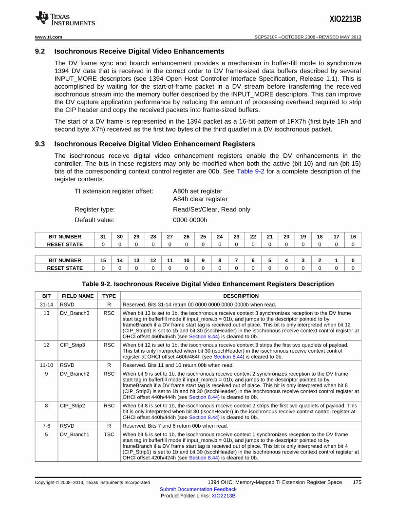
XIO2213B
www.ti.com SCPS210F –OCTOBER 2008–REVISED MAY 2013
9.2 Isochronous Receive Digital Video Enhancements
The DV frame sync and branch enhancement provides a mechanism in buffer-fill mode to synchronize1394 DV data that is received in the correct order to DV frame-sized data buffers described by severalINPUT_MORE descriptors (see 1394 Open Host Controller Interface Specification, Release 1.1). This isaccomplished by waiting for the start-of-frame packet in a DV stream before transferring the receivedisochronous stream into the memory buffer described by the INPUT_MORE descriptors. This can improvethe DV capture application performance by reducing the amount of processing overhead required to stripthe CIP header and copy the received packets into frame-sized buffers.
The start of a DV frame is represented in the 1394 packet as a 16-bit pattern of 1FX7h (first byte 1Fh andsecond byte X7h) received as the first two bytes of the third quadlet in a DV isochronous packet.
9.3 Isochronous Receive Digital Video Enhancement Registers
The isochronous receive digital video enhancement registers enable the DV enhancements in thecontroller. The bits in these registers may only be modified when both the active (bit 10) and run (bit 15)bits of the corresponding context control register are 00b. See Table 9-2 for a complete description of theregister contents.
TI extension register offset: A80h set registerA84h clear register
Register type: Read/Set/Clear, Read only
Default value: 0000 0000h
BIT NUMBER 31 30 29 28 27 26 25 24 23 22 21 20 19 18 17 16
RESET STATE 0 0 0 0 0 0 0 0 0 0 0 0 0 0 0 0
BIT NUMBER 15 14 13 12 11 10 9 8 7 6 5 4 3 2 1 0
RESET STATE 0 0 0 0 0 0 0 0 0 0 0 0 0 0 0 0
Table 9-2. Isochronous Receive Digital Video Enhancement Registers Description
BIT FIELD NAME TYPE DESCRIPTION
31-14 RSVD R Reserved. Bits 31-14 return 00 0000 0000 0000 0000b when read.
13 DV_Branch3 RSC When bit 13 is set to 1b, the isochronous receive context 3 synchronizes reception to the DV framestart tag in bufferfill mode if input_more.b = 01b, and jumps to the descriptor pointed to byframeBranch if a DV frame start tag is received out of place. This bit is only interpreted when bit 12(CIP_Strip3) is set to 1b and bit 30 (isochHeader) in the isochronous receive context control register atOHCI offset 460h/464h (see Section 8.44) is cleared to 0b.
12 CIP_Strip3 RSC When bit 12 is set to 1b, the isochronous receive context 3 strips the first two quadlets of payload.This bit is only interpreted when bit 30 (isochHeader) in the isochronous receive context controlregister at OHCI offset 460h/464h (see Section 8.44) is cleared to 0b.
11-10 RSVD R Reserved. Bits 11 and 10 return 00b when read.
9 DV_Branch2 RSC When bit 9 is set to 1b, the isochronous receive context 2 synchronizes reception to the DV framestart tag in bufferfill mode if input_more.b = 01b, and jumps to the descriptor pointed to byframeBranch if a DV frame start tag is received out of place. This bit is only interpreted when bit 8(CIP_Strip2) is set to 1b and bit 30 (isochHeader) in the isochronous receive context control register atOHCI offset 440h/444h (see Section 8.44) is cleared to 0b.
8 CIP_Strip2 RSC When bit 8 is set to 1b, the isochronous receive context 2 strips the first two quadlets of payload. Thisbit is only interpreted when bit 30 (isochHeader) in the isochronous receive context control register atOHCI offset 440h/444h (see Section 8.44) is cleared to 0b.
7-6 RSVD R Reserved. Bits 7 and 6 return 00b when read.
5 DV_Branch1 TSC When bit 5 is set to 1b, the isochronous receive context 1 synchronizes reception to the DV framestart tag in bufferfill mode if input_more.b = 01b, and jumps to the descriptor pointed to byframeBranch if a DV frame start tag is received out of place. This bit is only interpreted when bit 4(CIP_Strip1) is set to 1b and bit 30 (isochHeader) in the isochronous receive context control register atOHCI offset 420h/424h (see Section 8.44) is cleared to 0b.
Copyright © 2008–2013, Texas Instruments Incorporated 1394 OHCI Memory-Mapped TI Extension Register Space 175Submit Documentation FeedbackProduct Folder Links: XIO2213B
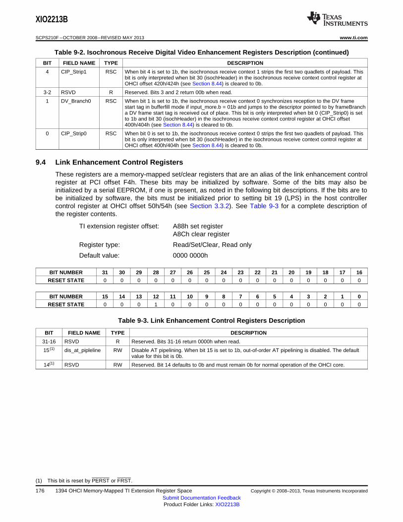
XIO2213B
SCPS210F –OCTOBER 2008–REVISED MAY 2013 www.ti.com
Table 9-2. Isochronous Receive Digital Video Enhancement Registers Description (continued)
BIT FIELD NAME TYPE DESCRIPTION
4 CIP_Strip1 RSC When bit 4 is set to 1b, the isochronous receive context 1 strips the first two quadlets of payload. Thisbit is only interpreted when bit 30 (isochHeader) in the isochronous receive context control register atOHCI offset 420h/424h (see Section 8.44) is cleared to 0b.
3-2 RSVD R Reserved. Bits 3 and 2 return 00b when read.
1 DV_Branch0 RSC When bit 1 is set to 1b, the isochronous receive context 0 synchronizes reception to the DV framestart tag in bufferfill mode if input_more.b = 01b and jumps to the descriptor pointed to by frameBrancha DV frame start tag is received out of place. This bit is only interpreted when bit 0 (CIP_Strip0) is setto 1b and bit 30 (isochHeader) in the isochronous receive context control register at OHCI offset400h/404h (see Section 8.44) is cleared to 0b.
0 CIP_Strip0 RSC When bit 0 is set to 1b, the isochronous receive context 0 strips the first two quadlets of payload. Thisbit is only interpreted when bit 30 (isochHeader) in the isochronous receive context control register atOHCI offset 400h/404h (see Section 8.44) is cleared to 0b.
9.4 Link Enhancement Control Registers
These registers are a memory-mapped set/clear registers that are an alias of the link enhancement controlregister at PCI offset F4h. These bits may be initialized by software. Some of the bits may also beinitialized by a serial EEPROM, if one is present, as noted in the following bit descriptions. If the bits are tobe initialized by software, the bits must be initialized prior to setting bit 19 (LPS) in the host controllercontrol register at OHCI offset 50h/54h (see Section 3.3.2). See Table 9-3 for a complete description ofthe register contents.
TI extension register offset: A88h set registerA8Ch clear register
Register type: Read/Set/Clear, Read only
Default value: 0000 0000h
BIT NUMBER 31 30 29 28 27 26 25 24 23 22 21 20 19 18 17 16
RESET STATE 0 0 0 0 0 0 0 0 0 0 0 0 0 0 0 0
BIT NUMBER 15 14 13 12 11 10 9 8 7 6 5 4 3 2 1 0
RESET STATE 0 0 0 1 0 0 0 0 0 0 0 0 0 0 0 0
Table 9-3. Link Enhancement Control Registers Description
BIT FIELD NAME TYPE DESCRIPTION
31-16 RSVD R Reserved. Bits 31-16 return 0000h when read.
15 (1) dis_at_pipleline RW Disable AT pipelining. When bit 15 is set to 1b, out-of-order AT pipelining is disabled. The defaultvalue for this bit is 0b.
14(1) RSVD RW Reserved. Bit 14 defaults to 0b and must remain 0b for normal operation of the OHCI core.
(1) This bit is reset by PERST or FRST.
176 1394 OHCI Memory-Mapped TI Extension Register Space Copyright © 2008–2013, Texas Instruments Incorporated
Submit Documentation FeedbackProduct Folder Links: XIO2213B
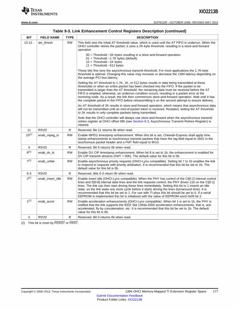
XIO2213B
www.ti.com SCPS210F –OCTOBER 2008–REVISED MAY 2013
Table 9-3. Link Enhancement Control Registers Description (continued)
BIT FIELD NAME TYPE DESCRIPTION
13-12 (2) atx_thresh RW This field sets the initial AT threshold value, which is used until the AT FIFO is underrun. When theOHCI controller retries the packet, it uses a 2K-byte threshold, resulting in a store-and-forwardoperation.
00 = Threshold ~2K bytes resulting in a store-and-forward operation01 = Threshold ~1.7K bytes (default)10 = Threshold ~1K bytes11 = Threshold ~512 bytes
These bits fine tune the asynchronous transmit threshold. For most applications the 1.7K-bytethreshold is optimal. Changing this value may increase or decrease the 1394 latency depending onthe average PCI bus latency.
Setting the AT threshold to 1.7K, 1K, or 512 bytes results in data being transmitted at thesethresholds or when an entire packet has been checked into the FIFO. If the packet to betransmitted is larger than the AT threshold, the remaining data must be received before the ATFIFO is emptied; otherwise, an underrun condition occurs, resulting in a packet error at thereceiving node. As a result, the link then commences store-and-forward operation. Wait until it hasthe complete packet in the FIFO before retransmitting it on the second attempt to ensure delivery.
An AT threshold of 2K results in store-and-forward operation, which means that asynchronous datawill not be transmitted until an end-of-packet token is received. Restated, setting the AT thresholdto 2K results in only complete packets being transmitted.
Note that the OHCI controller will always use store-and-forward when the asynchronous transmitretries register at OHCI offset 08h (see Section 8.3, Asynchronous Transmit Retries Register) iscleared.
11 RSVD R Reserved. Bit 11 returns 0b when read.
10(1) enab_mpeg_ts RW Enable MPEG timestamp enhancement. When this bit is set, Cheetah-Express shall apply timestamp enhancements to isochronous transmit packets that have the tag field equal to 2b01 in theisochronous packet header and a FMT field equal to 6h10.
9 RSVD R Reserved. Bit 9 returns 0b when read.
8(1) enab_dv_ts RW Enable DV CIP timestamp enhancement. When bit 8 is set to 1b, the enhancement is enabled forDV CIP transmit streams (FMT = 00h). The default value for this bit is 0b.
7(1) enab_unfair RW Enable asynchronous priority requests (OHCI-Lynx compatible). Setting bit 7 to 1b enables the linkto respond to requests with priority arbitration. It is recommended that this bit be set to 1b. Thedefault value for this bit is 0b.
6-3 RSVD R Reserved. Bits 6-3 return 0h when read.
2(1) enab_insert_idle RW Enable insert idle (OHCI-Lynx compatible). When the PHY has control of the Ct[0:1] internal controllines and D[0:8] internal data lines and the link requests control, the PHY drives 11b on the Ct[0:1]lines. The link can then start driving these lines immediately. Setting this bit to 1 inserts an idlestate, so the link waits one clock cycle before it starts driving the lines (turnaround time). It isrecommended that this bit be set to 1. For use with TI phys this bit should be set to 0. If a serialEEPROM is implemented this bit is initialized with the value of EEPROM word 0x05 bit 2.
1(1) enab_accel RW Enable acceleration enhancements (OHCI-Lynx compatible). When bit 1 is set to 1b, the PHY isnotified that the link supports the IEEE Std 1394a-2000 acceleration enhancements, that is, ack-accelerated, fly-by concatenation, etc. It is recommended that this bit be set to 1b. The defaultvalue for this bit is 0b.
0 RSVD R Reserved. Bit 0 returns 0b when read.
(2) This bit is reset by PERST or FRST.
Copyright © 2008–2013, Texas Instruments Incorporated 1394 OHCI Memory-Mapped TI Extension Register Space 177Submit Documentation FeedbackProduct Folder Links: XIO2213B
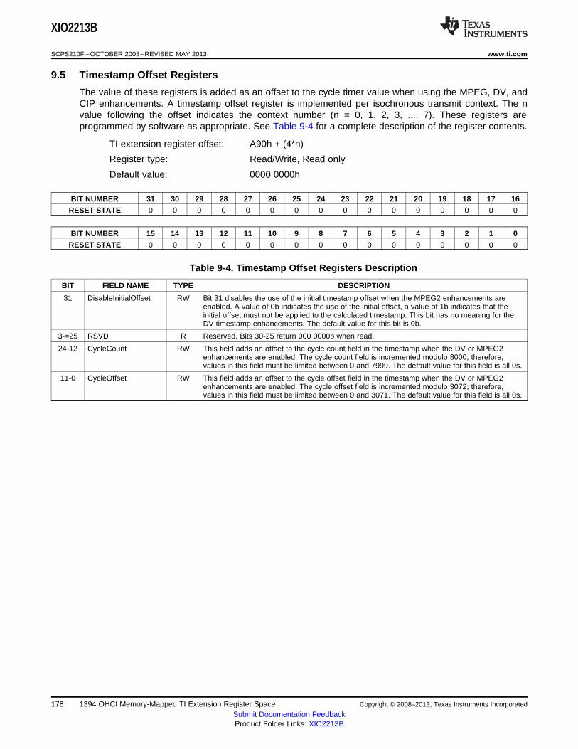
XIO2213B
SCPS210F –OCTOBER 2008–REVISED MAY 2013 www.ti.com
9.5 Timestamp Offset Registers
The value of these registers is added as an offset to the cycle timer value when using the MPEG, DV, andCIP enhancements. A timestamp offset register is implemented per isochronous transmit context. The nvalue following the offset indicates the context number (n = 0, 1, 2, 3, ..., 7). These registers areprogrammed by software as appropriate. See Table 9-4 for a complete description of the register contents.
TI extension register offset: A90h + (4*n)
Register type: Read/Write, Read only
Default value: 0000 0000h
BIT NUMBER 31 30 29 28 27 26 25 24 23 22 21 20 19 18 17 16
RESET STATE 0 0 0 0 0 0 0 0 0 0 0 0 0 0 0 0
BIT NUMBER 15 14 13 12 11 10 9 8 7 6 5 4 3 2 1 0
RESET STATE 0 0 0 0 0 0 0 0 0 0 0 0 0 0 0 0
Table 9-4. Timestamp Offset Registers Description
BIT FIELD NAME TYPE DESCRIPTION
31 DisableInitialOffset RW Bit 31 disables the use of the initial timestamp offset when the MPEG2 enhancements areenabled. A value of 0b indicates the use of the initial offset, a value of 1b indicates that theinitial offset must not be applied to the calculated timestamp. This bit has no meaning for theDV timestamp enhancements. The default value for this bit is 0b.
3-=25 RSVD R Reserved. Bits 30-25 return 000 0000b when read.
24-12 CycleCount RW This field adds an offset to the cycle count field in the timestamp when the DV or MPEG2enhancements are enabled. The cycle count field is incremented modulo 8000; therefore,values in this field must be limited between 0 and 7999. The default value for this field is all 0s.
11-0 CycleOffset RW This field adds an offset to the cycle offset field in the timestamp when the DV or MPEG2enhancements are enabled. The cycle offset field is incremented modulo 3072; therefore,values in this field must be limited between 0 and 3071. The default value for this field is all 0s.
178 1394 OHCI Memory-Mapped TI Extension Register Space Copyright © 2008–2013, Texas Instruments Incorporated
Submit Documentation FeedbackProduct Folder Links: XIO2213B
XIO2213B
www.ti.com SCPS210F –OCTOBER 2008–REVISED MAY 2013
10 Physical Layer (PHY) Section
The cable interface can follow either the IEEE Std 1394a-2000 protocol or the IEEE Std 1394b-2002protocol on all ports. The mode of operation is determined by the interface capabilities of the portsbeing connected. When either of the ports is connected to an IEEE Std 1394a-2000-compliant device,the cable interface on that port operates in the IEEE Std 1394a-2000 data-strobe mode at a compatibleS100, S200, or S400 speed. When a bilingual port is connected to an IEEE Std 1394b-2002-compliantnode, the cable interface on that port operates per the IEEE Std 1394b-2002 standard at S400B orS800 speed. The XIO2213B automatically determines the correct cable interface connection methodfor the bilingual ports.To operate a port as an IEEE Std 1394b-2002 bilingual port, the data-strobe-only terminal for the port(DS0, DS1, or DS2_P ) must be pulled to ground through a 1-kΩ resistor. The port must be operated inthe IEEE Std 1394b-2002 bilingual mode whenever an IEEE Std 1394b-2002 bilingual or an IEEE Std1394b-2002 beta-only connector is connected to the port. To operate the port as an IEEE Std 1394a-2000-only port, the data-strobe-only terminal (DS0, DS1, or DS2_P) must be pulled to 3.3-V VCCthrough a 1-kΩ resistor. The only time the port must be forced to the data-strobe-only mode is if theport is connected to an IEEE Std 1394a-2000 connector [either 6 pin (recommended) or 4 pin]. Thismode is provided to ensure that IEEE Std 1394b-2002 signaling is never sent across an IEEE Std1394a-2000 cable.During packet reception, the serial data bits are split into 2-, 4-, or 8-bit parallel streams by the PHYsection and sent to the link-layer controller (LLC) section. The received data is also transmitted(repeated) on the other connected and active cable ports.Both the twisted pair A (TPA) and the twisted pair B (TPB) cable interfaces incorporate differentialcomparators to monitor the line states during initialization and arbitration when connected to an IEEEStd 1394a-2000-compliant device. The outputs of these comparators are used by the internal logic todetermine the arbitration status. The TPA channel monitors the incoming cable common-mode voltage.The value of this common-mode voltage is used during IEEE Std 1394a-2000-mode arbitration andsets the speed of the next packet transmission. In addition, the TPB channel monitors the incomingcable common-mode voltage on the TPB pair for the presence of the remotely supplied twisted pairbias (TPBIAS) voltage.When connected to an IEEE Std 1394a-2000-compliant node, the XIO2213B PHY section provides a1.86-V nominal bias voltage at the TPBIAS terminal for port termination. The PHY section containsthree independent TPBIAS circuits (one for each port). This bias voltage, when seen through a cableby a remote receiver, indicates the presence of an active connection. This bias voltage source must bestabilized by an external filter capacitor of 1 μF.The line drivers in the XIO2213B PHY section are designed to work with external 112-Ω terminationresistor networks in order to match the 110-Ω cable impedance. One termination network is required ateach end of a twisted-pair cable. Each network is composed of a pair of series-connected 56-Ωresistors. The midpoint of the pair of resistors that is connected to the TPA terminals is connected to itscorresponding TPBIAS voltage terminal. The midpoint of the pair of resistors that is directly connectedto the TPB terminals is coupled to ground through a parallel RC network, with recommended values of5 k and 270 pF. The values of the external line-termination resistors are selected to meet the standardspecifications when connected in parallel with the internal receiver circuits. A precision external resistorconnected between the R0 and R1 terminals sets the driver output current, along with other internaloperating currents.When the power supply of the XIO2213B is off while the twisted-pair cables are connected, theXIO2213B transmitter and receiver circuitry present to the cable a high-impedance signal that does notload the device at the other end of the cable.
Copyright © 2008–2013, Texas Instruments Incorporated Physical Layer (PHY) Section 179Submit Documentation FeedbackProduct Folder Links: XIO2213B
XIO2213B
SCPS210F –OCTOBER 2008–REVISED MAY 2013 www.ti.com
When the XIO2213B PHY section is used without one or more of the ports brought out to a connector,the twisted-pair terminals of the unused ports must be terminated for reliable operation. For eachunused port, the port must be forced to the IEEE Std 1394a-2000-only mode (data-strobe-only mode)by pulling DSn to VCC through a 1KΩ resistor, after which the TPB+ and TPB– terminals can be tiedtogether and then pulled to ground; or TPB+ and TPB– can be connected to the suggested normaltermination network. TPA+ and TPA– of an unused port can be left unconnected. The TPBIAS terminalcan be connected through a 1-μF capacitor to ground or left unconnected.The TESTM, SE, and SM terminals are used to set up various manufacturing test conditions. Fornormal operation, TESTM must be connected to VDD through a 1-kΩ resistor. The SE and SMterminals must be tied to ground through a 1-kΩ resistor.The LPS_P (link power status) terminal of the PHY section works with the LKON terminal to managethe power usage in the node. The LPS_L signal from the LLC section is used in conjunction with theLCtrl bit (see Table 10-1 and Table 10-2 ) to indicate the active/power status of the LLC section. TheLPS_P signal also resets, disables, and initializes the PHY-section/LLC-section interface (the state ofthe PHY-section/LLC-section interface is controlled solely by the LPS_P input, regardless of the stateof the LCtrl bit). The LPS_P terminal of the PHY section must be connected to the LPS_L terminal ofthe LLC section during normal operation.The LPS_P input is considered inactive if it remains low for more than the PHY_RESET time (see theLPS terminal definition) and is considered active otherwise. When the PHY section detects that theLPS_P input is inactive, the PHY-section/LLC-section interface is placed into a low-power reset state inwhich the CTL and D outputs are held in the logic 0 state and the LREQ input is ignored; however, thePCLK output remains active. If the LPS input remains low for more than the LPS_DISABLE time (seethe LPS terminal definition), the PHY-section/LLC-section interface is put into a low-power disabledstate in which the PCLK_P output is also held inactive. The XIO2213B continues the necessary PHYrepeater functions required for normal network operation, regardless of the state of the PHY-section/LLC-section interface. When the interface is in the reset or disabled state and the LPS input isagain observed active, the PHY section initializes the interface and returns to normal operation. ThePHY-section/LLC-section interface is also held in the disabled state during hardware reset. When theLPS_P terminal is returned to an active state after being sensed as having entered the LPS_DISABLEtime, the XIO2213B issues a bus reset. This broadcasts the node self-ID packet, which contains theupdated L bit state (the PHY section and LLC section now being accessible).The PHY section uses the LKON terminal to notify the LLC section to power up and become active.When activated, the output LKON signal is a square wave. The PHY section activates the LKONoutput when the LLC section is inactive and a wake-up event occurs. The LLC section is consideredinactive when either the LPS_P input is inactive, as previously described, or the LCtrl bit is cleared to0. A wake-up event occurs when a link-on PHY packet addressed to this node is received, orconditionally when a PHY interrupt occurs. The PHY section deasserts the LKON output when the LLCsection becomes active (both LPS_P sensed as active and the LCtrl bit set to 1). The PHY section alsodeasserts the LKON output when a bus reset occurs, unless a PHY interrupt condition exists, whichwould otherwise cause LKON to be active. If the XIO2213B is power cycled and the power class is 0through 4, the PHY section asserts LKON for approximately 167 ms or until both the LPS_P is activeand the LCtrl bit is 1.
10.1 PHY Section Register Configuration
There are 16 accessible PHY section registers in the XIO2213B. The configuration of the registers ataddresses 0h through 7h (the base registers) is fixed, while the configuration of the registers at addresses8h through Fh (the paged registers) is dependent on which of eight pages, numbered 0h through 7h, iscurrently selected. The selected page is set in base register 7h. Note that while this register set iscompatible with IEEE Std 1394a-2000 register sets, some fields have been redefined and this register setcontains additional fields.
Table 10-1 shows the configuration of the base registers, and Table 10-2 gives the corresponding fielddescriptions. The base register field definitions are unaffected by the selected page number.
180 Physical Layer (PHY) Section Copyright © 2008–2013, Texas Instruments Incorporated
Submit Documentation FeedbackProduct Folder Links: XIO2213B
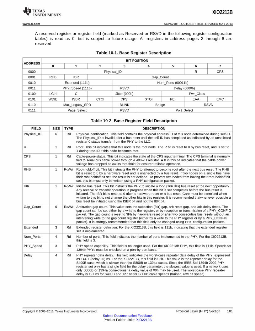
XIO2213B
www.ti.com SCPS210F –OCTOBER 2008–REVISED MAY 2013
A reserved register or register field (marked as Reserved or RSVD in the following register configurationtables) is read as 0, but is subject to future usage. All registers in address pages 2 through 6 arereserved.
Table 10-1. Base Register Description
BIT POSITIONADDRESS
0 1 2 3 4 5 6 7
0000 Physical_ID R CPS
0001 RHB IBR Gap_Count
0010 Extended (111b) Num_Ports (00011b)
0011 PHY_Speed (111b) RSVD Delay (0000b)
0100 LCtrl C Jitter (000b) Pwr_Class
0101 WDIE ISBR CTOI CPSI STOI PEI EAA EMC
0110 Max_Legacy_SPD BLINK Bridge RSVD
0111 Page_Select RSVD Port_Select
Table 10-2. Base Register Field Description
FIELD SIZE TYPE DESCRIPTION
Physical_ID 6 Rd Physical identification. This field contains the physical address ID of this node determined during self-ID.The Physical_ID is invalid after a bus reset until the self-ID has completed as indicated by an unsolicitedregister 0 status transfer from the PHY to the LLC.
R 1 Rd Root. This bit indicates that this node is the root node. The R bit is reset to 0 by bus reset, and is set to1 during tree-ID if this node becomes root.
CPS 1 Rd Cable-power-status. This bit indicates the state of the CPS input terminal. The CPS terminal is normallytied to serial bus cable power through a 400-kΩ resistor. A 0 in this bit indicates that the cable powervoltage has dropped below its threshold for ensured reliable operation.
RHB 1 Rd/Wr Root-holdoff bit. This bit instructs the PHY to attempt to become root after the next bus reset. The RHBbit is reset to 0 by a hardware reset and is unaffected by a bus reset. If two nodes on a single bus havetheir root holdoff bit set, the result is not defined. To prevent two nodes from having their root-holdoff bitset, this bit must only be written using a PHY configuration packet.
IBR 1 Rd/Wr Initiate bus reset. This bit instructs the PHY to initiate a long (166 s) bus reset at the next opportunity.Any receive or transmit operation in progress when this bit is set completes before the bus reset isinitiated. The IBR bit is reset to 0 after a hardware reset or a bus reset. Care must be exercised whenwriting to this bit to not change the other bits in this register. It is recommended thatwhenever possible abus reset be initiated using the ISBR bit and not the IBR bit.
Gap_Count 6 Rd/Wr Arbitration gap count. This value sets the subaction (fair) gap, arb-reset gap, and arb-delay times. Thegap count can be set either by a write to the register, or by reception or transmission of a PHY_CONFIGpacket. The gap count is reset to 3Fh by hardware reset or after two consecutive bus resets without anintervening write to the gap count register (either by a write to the PHY register or by a PHY_CONFIGpacket). It is strongly recommended that this field only be changed using PHY configuration packets.
Extended 3 Rd Extended register definition. For the XIO2213B, this field is 111b, indicating that the extended registerset is implemented.
Num_Ports 4 Rd Number of ports. This field indicates the number of ports implemented in the PHY. For the XIO2213B,this field is 3.
PHY_Speed 3 Rd PHY speed capability. This field is no longer used. For the XIO2213B PHY, this field is 111b. Speeds for1394b PHYs must be checked on a port-by-port basis.
Delay 4 Rd PHY repeater data delay. This field indicates the worst-case repeater data delay of the PHY, expressedas 144 + (delay 20) ns. For the XIO2213B, this field is 02h. This value is the repeater delay for theS400B case, which is slower than the S800B or 1394a cases. Since the IEEE Std 1394b-2002 PHYregister set only has a single field for the delay parameter, the slowest value is used. If a network usesonly S800B or 1394a connections, a delay value of 00h may be used. The worst-case PHY repeaterdelay is 197 ns for S400B and 127 ns for S800B cable speeds (trained, raw bit speed).
Copyright © 2008–2013, Texas Instruments Incorporated Physical Layer (PHY) Section 181Submit Documentation FeedbackProduct Folder Links: XIO2213B
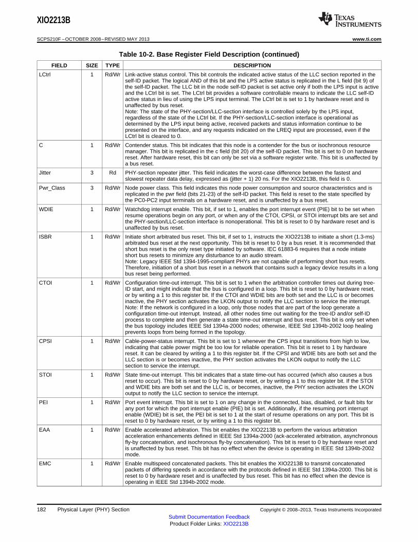
XIO2213B
SCPS210F –OCTOBER 2008–REVISED MAY 2013 www.ti.com
Table 10-2. Base Register Field Description (continued)
FIELD SIZE TYPE DESCRIPTION
LCtrl 1 Rd/Wr Link-active status control. This bit controls the indicated active status of the LLC section reported in theself-ID packet. The logical AND of this bit and the LPS active status is replicated in the L field (bit 9) ofthe self-ID packet. The LLC bit in the node self-ID packet is set active only if both the LPS input is activeand the LCtrl bit is set. The LCtrl bit provides a software controllable means to indicate the LLC self-IDactive status in lieu of using the LPS input terminal. The LCtrl bit is set to 1 by hardware reset and isunaffected by bus reset.Note: The state of the PHY-section/LLC-section interface is controlled solely by the LPS input,regardless of the state of the LCtrl bit. If the PHY-section/LLC-section interface is operational asdetermined by the LPS input being active, received packets and status information continue to bepresented on the interface, and any requests indicated on the LREQ input are processed, even if theLCtrl bit is cleared to 0.
C 1 Rd/Wr Contender status. This bit indicates that this node is a contender for the bus or isochronous resourcemanager. This bit is replicated in the c field (bit 20) of the self-ID packet. This bit is set to 0 on hardwarereset. After hardware reset, this bit can only be set via a software register write. This bit is unaffected bya bus reset.
Jitter 3 Rd PHY-section repeater jitter. This field indicates the worst-case difference between the fastest andslowest repeater data delay, expressed as (jitter + 1) 20 ns. For the XIO2213B, this field is 0.
Pwr_Class 3 Rd/Wr Node power class. This field indicates this node power consumption and source characteristics and isreplicated in the pwr field (bits 21-23) of the self-ID packet. This field is reset to the state specified bythe PC0-PC2 input terminals on a hardware reset, and is unaffected by a bus reset.
WDIE 1 Rd/Wr Watchdog interrupt enable. This bit, if set to 1, enables the port interrupt event (PIE) bit to be set whenresume operations begin on any port, or when any of the CTOI, CPSI, or STOI interrupt bits are set andthe PHY-section/LLC-section interface is nonoperational. This bit is reset to 0 by hardware reset and isunaffected by bus reset.
ISBR 1 Rd/Wr Initiate short arbitrated bus reset. This bit, if set to 1, instructs the XIO2213B to initiate a short (1.3-ms)arbitrated bus reset at the next opportunity. This bit is reset to 0 by a bus reset. It is recommended thatshort bus reset is the only reset type initiated by software. IEC 61883-6 requires that a node initiateshort bus resets to minimize any disturbance to an audio stream.Note: Legacy IEEE Std 1394-1995-compliant PHYs are not capable of performing short bus resets.Therefore, initiation of a short bus reset in a network that contains such a legacy device results in a longbus reset being performed.
CTOI 1 Rd/Wr Configuration time-out interrupt. This bit is set to 1 when the arbitration controller times out during tree-ID start, and might indicate that the bus is configured in a loop. This bit is reset to 0 by hardware reset,or by writing a 1 to this register bit. If the CTOI and WDIE bits are both set and the LLC is or becomesinactive, the PHY section activates the LKON output to notify the LLC section to service the interrupt.Note: If the network is configured in a loop, only those nodes that are part of the loop generate aconfiguration time-out interrupt. Instead, all other nodes time out waiting for the tree-ID and/or self-IDprocess to complete and then generate a state time-out interrupt and bus reset. This bit is only set whenthe bus topology includes IEEE Std 1394a-2000 nodes; otherwise, IEEE Std 1394b-2002 loop healingprevents loops from being formed in the topology.
CPSI 1 Rd/Wr Cable-power-status interrupt. This bit is set to 1 whenever the CPS input transitions from high to low,indicating that cable power might be too low for reliable operation. This bit is reset to 1 by hardwarereset. It can be cleared by writing a 1 to this register bit. If the CPSI and WDIE bits are both set and theLLC section is or becomes inactive, the PHY section activates the LKON output to notify the LLCsection to service the interrupt.
STOI 1 Rd/Wr State time-out interrupt. This bit indicates that a state time-out has occurred (which also causes a busreset to occur). This bit is reset to 0 by hardware reset, or by writing a 1 to this register bit. If the STOIand WDIE bits are both set and the LLC is, or becomes, inactive, the PHY section activates the LKONoutput to notify the LLC section to service the interrupt.
PEI 1 Rd/Wr Port event interrupt. This bit is set to 1 on any change in the connected, bias, disabled, or fault bits forany port for which the port interrupt enable (PIE) bit is set. Additionally, if the resuming port interruptenable (WDIE) bit is set, the PEI bit is set to 1 at the start of resume operations on any port. This bit isreset to 0 by hardware reset, or by writing a 1 to this register bit.
EAA 1 Rd/Wr Enable accelerated arbitration. This bit enables the XIO2213B to perform the various arbitrationacceleration enhancements defined in IEEE Std 1394a-2000 (ack-accelerated arbitration, asynchronousfly-by concatenation, and isochronous fly-by concatenation). This bit is reset to 0 by hardware reset andis unaffected by bus reset. This bit has no effect when the device is operating in IEEE Std 1394b-2002mode.
EMC 1 Rd/Wr Enable multispeed concatenated packets. This bit enables the XIO2213B to transmit concatenatedpackets of differing speeds in accordance with the protocols defined in IEEE Std 1394a-2000. This bit isreset to 0 by hardware reset and is unaffected by bus reset. This bit has no effect when the device isoperating in IEEE Std 1394b-2002 mode.
182 Physical Layer (PHY) Section Copyright © 2008–2013, Texas Instruments Incorporated
Submit Documentation FeedbackProduct Folder Links: XIO2213B
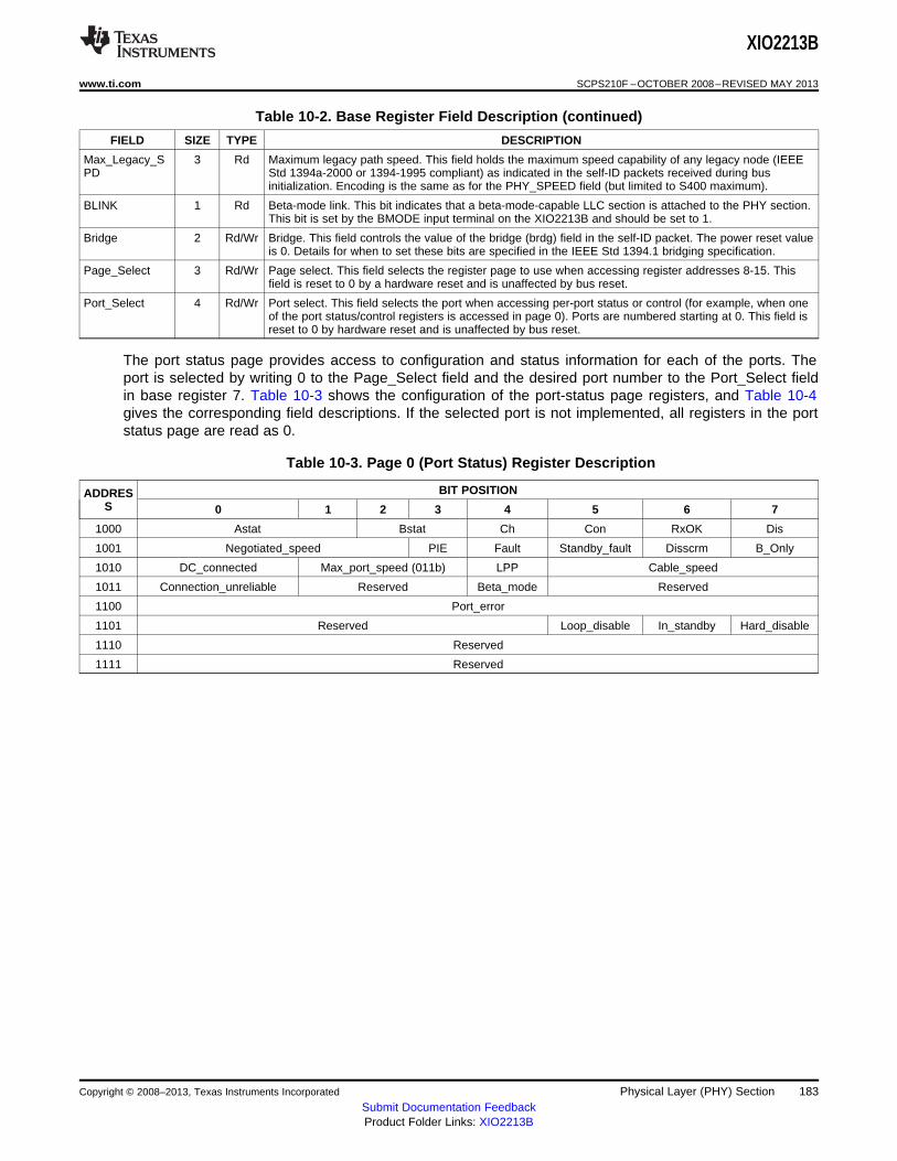
XIO2213B
www.ti.com SCPS210F –OCTOBER 2008–REVISED MAY 2013
Table 10-2. Base Register Field Description (continued)
FIELD SIZE TYPE DESCRIPTION
Max_Legacy_S 3 Rd Maximum legacy path speed. This field holds the maximum speed capability of any legacy node (IEEEPD Std 1394a-2000 or 1394-1995 compliant) as indicated in the self-ID packets received during bus
initialization. Encoding is the same as for the PHY_SPEED field (but limited to S400 maximum).
BLINK 1 Rd Beta-mode link. This bit indicates that a beta-mode-capable LLC section is attached to the PHY section.This bit is set by the BMODE input terminal on the XIO2213B and should be set to 1.
Bridge 2 Rd/Wr Bridge. This field controls the value of the bridge (brdg) field in the self-ID packet. The power reset valueis 0. Details for when to set these bits are specified in the IEEE Std 1394.1 bridging specification.
Page_Select 3 Rd/Wr Page select. This field selects the register page to use when accessing register addresses 8-15. Thisfield is reset to 0 by a hardware reset and is unaffected by bus reset.
Port_Select 4 Rd/Wr Port select. This field selects the port when accessing per-port status or control (for example, when oneof the port status/control registers is accessed in page 0). Ports are numbered starting at 0. This field isreset to 0 by hardware reset and is unaffected by bus reset.
The port status page provides access to configuration and status information for each of the ports. Theport is selected by writing 0 to the Page_Select field and the desired port number to the Port_Select fieldin base register 7. Table 10-3 shows the configuration of the port-status page registers, and Table 10-4gives the corresponding field descriptions. If the selected port is not implemented, all registers in the portstatus page are read as 0.
Table 10-3. Page 0 (Port Status) Register Description
BIT POSITIONADDRESS 0 1 2 3 4 5 6 7
1000 Astat Bstat Ch Con RxOK Dis
1001 Negotiated_speed PIE Fault Standby_fault Disscrm B_Only
1010 DC_connected Max_port_speed (011b) LPP Cable_speed
1011 Connection_unreliable Reserved Beta_mode Reserved
1100 Port_error
1101 Reserved Loop_disable In_standby Hard_disable
1110 Reserved
1111 Reserved
Copyright © 2008–2013, Texas Instruments Incorporated Physical Layer (PHY) Section 183Submit Documentation FeedbackProduct Folder Links: XIO2213B
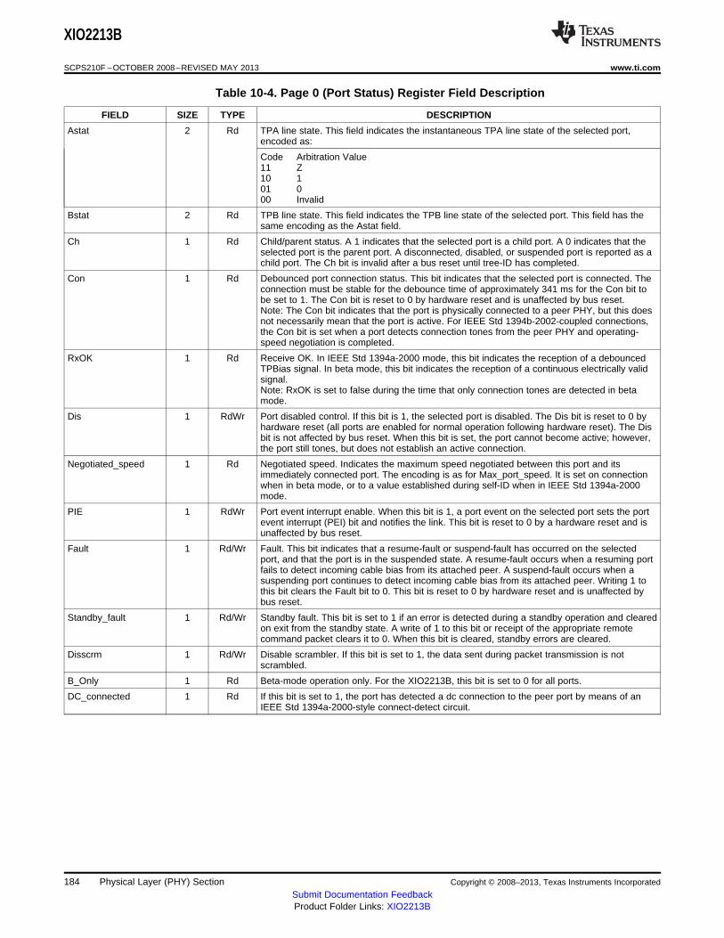
XIO2213B
SCPS210F –OCTOBER 2008–REVISED MAY 2013 www.ti.com
Table 10-4. Page 0 (Port Status) Register Field Description
FIELD SIZE TYPE DESCRIPTION
Astat 2 Rd TPA line state. This field indicates the instantaneous TPA line state of the selected port,encoded as:
Code Arbitration Value11 Z10 101 000 Invalid
Bstat 2 Rd TPB line state. This field indicates the TPB line state of the selected port. This field has thesame encoding as the Astat field.
Ch 1 Rd Child/parent status. A 1 indicates that the selected port is a child port. A 0 indicates that theselected port is the parent port. A disconnected, disabled, or suspended port is reported as achild port. The Ch bit is invalid after a bus reset until tree-ID has completed.
Con 1 Rd Debounced port connection status. This bit indicates that the selected port is connected. Theconnection must be stable for the debounce time of approximately 341 ms for the Con bit tobe set to 1. The Con bit is reset to 0 by hardware reset and is unaffected by bus reset.Note: The Con bit indicates that the port is physically connected to a peer PHY, but this doesnot necessarily mean that the port is active. For IEEE Std 1394b-2002-coupled connections,the Con bit is set when a port detects connection tones from the peer PHY and operating-speed negotiation is completed.
RxOK 1 Rd Receive OK. In IEEE Std 1394a-2000 mode, this bit indicates the reception of a debouncedTPBias signal. In beta mode, this bit indicates the reception of a continuous electrically validsignal.Note: RxOK is set to false during the time that only connection tones are detected in betamode.
Dis 1 RdWr Port disabled control. If this bit is 1, the selected port is disabled. The Dis bit is reset to 0 byhardware reset (all ports are enabled for normal operation following hardware reset). The Disbit is not affected by bus reset. When this bit is set, the port cannot become active; however,the port still tones, but does not establish an active connection.
Negotiated_speed 1 Rd Negotiated speed. Indicates the maximum speed negotiated between this port and itsimmediately connected port. The encoding is as for Max_port_speed. It is set on connectionwhen in beta mode, or to a value established during self-ID when in IEEE Std 1394a-2000mode.
PIE 1 RdWr Port event interrupt enable. When this bit is 1, a port event on the selected port sets the portevent interrupt (PEI) bit and notifies the link. This bit is reset to 0 by a hardware reset and isunaffected by bus reset.
Fault 1 Rd/Wr Fault. This bit indicates that a resume-fault or suspend-fault has occurred on the selectedport, and that the port is in the suspended state. A resume-fault occurs when a resuming portfails to detect incoming cable bias from its attached peer. A suspend-fault occurs when asuspending port continues to detect incoming cable bias from its attached peer. Writing 1 tothis bit clears the Fault bit to 0. This bit is reset to 0 by hardware reset and is unaffected bybus reset.
Standby_fault 1 Rd/Wr Standby fault. This bit is set to 1 if an error is detected during a standby operation and clearedon exit from the standby state. A write of 1 to this bit or receipt of the appropriate remotecommand packet clears it to 0. When this bit is cleared, standby errors are cleared.
Disscrm 1 Rd/Wr Disable scrambler. If this bit is set to 1, the data sent during packet transmission is notscrambled.
B_Only 1 Rd Beta-mode operation only. For the XIO2213B, this bit is set to 0 for all ports.
DC_connected 1 Rd If this bit is set to 1, the port has detected a dc connection to the peer port by means of anIEEE Std 1394a-2000-style connect-detect circuit.
184 Physical Layer (PHY) Section Copyright © 2008–2013, Texas Instruments Incorporated
Submit Documentation FeedbackProduct Folder Links: XIO2213B
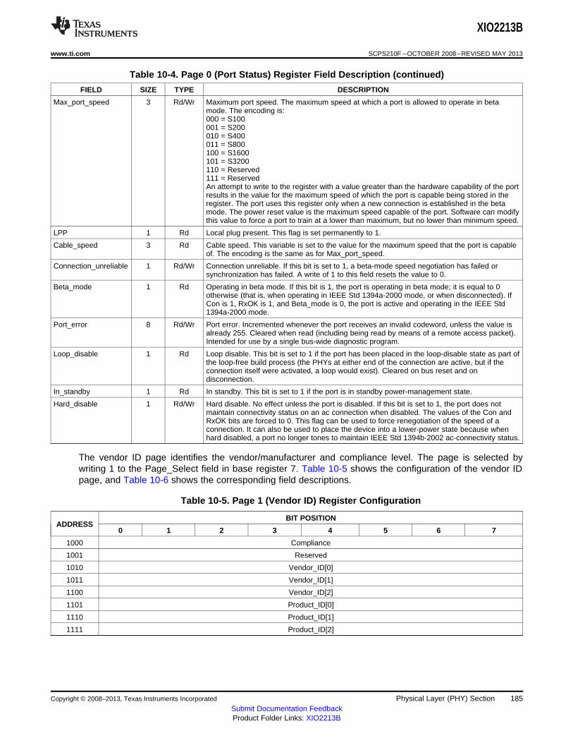
XIO2213B
www.ti.com SCPS210F –OCTOBER 2008–REVISED MAY 2013
Table 10-4. Page 0 (Port Status) Register Field Description (continued)
FIELD SIZE TYPE DESCRIPTION
Max_port_speed 3 Rd/Wr Maximum port speed. The maximum speed at which a port is allowed to operate in betamode. The encoding is:000 = S100001 = S200010 = S400011 = S800100 = S1600101 = S3200110 = Reserved111 = ReservedAn attempt to write to the register with a value greater than the hardware capability of the portresults in the value for the maximum speed of which the port is capable being stored in theregister. The port uses this register only when a new connection is established in the betamode. The power reset value is the maximum speed capable of the port. Software can modifythis value to force a port to train at a lower than maximum, but no lower than minimum speed.
LPP 1 Rd Local plug present. This flag is set permanently to 1.
Cable_speed 3 Rd Cable speed. This variable is set to the value for the maximum speed that the port is capableof. The encoding is the same as for Max_port_speed.
Connection_unreliable 1 Rd/Wr Connection unreliable. If this bit is set to 1, a beta-mode speed negotiation has failed orsynchronization has failed. A write of 1 to this field resets the value to 0.
Beta_mode 1 Rd Operating in beta mode. If this bit is 1, the port is operating in beta mode; it is equal to 0otherwise (that is, when operating in IEEE Std 1394a-2000 mode, or when disconnected). IfCon is 1, RxOK is 1, and Beta_mode is 0, the port is active and operating in the IEEE Std1394a-2000 mode.
Port_error 8 Rd/Wr Port error. Incremented whenever the port receives an invalid codeword, unless the value isalready 255. Cleared when read (including being read by means of a remote access packet).Intended for use by a single bus-wide diagnostic program.
Loop_disable 1 Rd Loop disable. This bit is set to 1 if the port has been placed in the loop-disable state as part ofthe loop-free build process (the PHYs at either end of the connection are active, but if theconnection itself were activated, a loop would exist). Cleared on bus reset and ondisconnection.
In_standby 1 Rd In standby. This bit is set to 1 if the port is in standby power-management state.
Hard_disable 1 Rd/Wr Hard disable. No effect unless the port is disabled. If this bit is set to 1, the port does notmaintain connectivity status on an ac connection when disabled. The values of the Con andRxOK bits are forced to 0. This flag can be used to force renegotiation of the speed of aconnection. It can also be used to place the device into a lower-power state because whenhard disabled, a port no longer tones to maintain IEEE Std 1394b-2002 ac-connectivity status.
The vendor ID page identifies the vendor/manufacturer and compliance level. The page is selected bywriting 1 to the Page_Select field in base register 7. Table 10-5 shows the configuration of the vendor IDpage, and Table 10-6 shows the corresponding field descriptions.
Table 10-5. Page 1 (Vendor ID) Register Configuration
BIT POSITIONADDRESS
0 1 2 3 4 5 6 7
1000 Compliance
1001 Reserved
1010 Vendor_ID[0]
1011 Vendor_ID[1]
1100 Vendor_ID[2]
1101 Product_ID[0]
1110 Product_ID[1]
1111 Product_ID[2]
Copyright © 2008–2013, Texas Instruments Incorporated Physical Layer (PHY) Section 185Submit Documentation FeedbackProduct Folder Links: XIO2213B
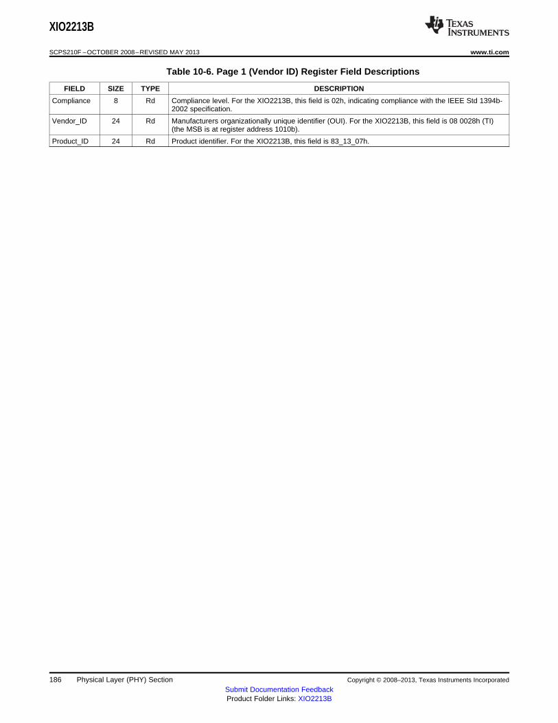
XIO2213B
SCPS210F –OCTOBER 2008–REVISED MAY 2013 www.ti.com
Table 10-6. Page 1 (Vendor ID) Register Field Descriptions
FIELD SIZE TYPE DESCRIPTION
Compliance 8 Rd Compliance level. For the XIO2213B, this field is 02h, indicating compliance with the IEEE Std 1394b-2002 specification.
Vendor_ID 24 Rd Manufacturers organizationally unique identifier (OUI). For the XIO2213B, this field is 08 0028h (TI)(the MSB is at register address 1010b).
Product_ID 24 Rd Product identifier. For the XIO2213B, this field is 83_13_07h.
186 Physical Layer (PHY) Section Copyright © 2008–2013, Texas Instruments Incorporated
Submit Documentation FeedbackProduct Folder Links: XIO2213B
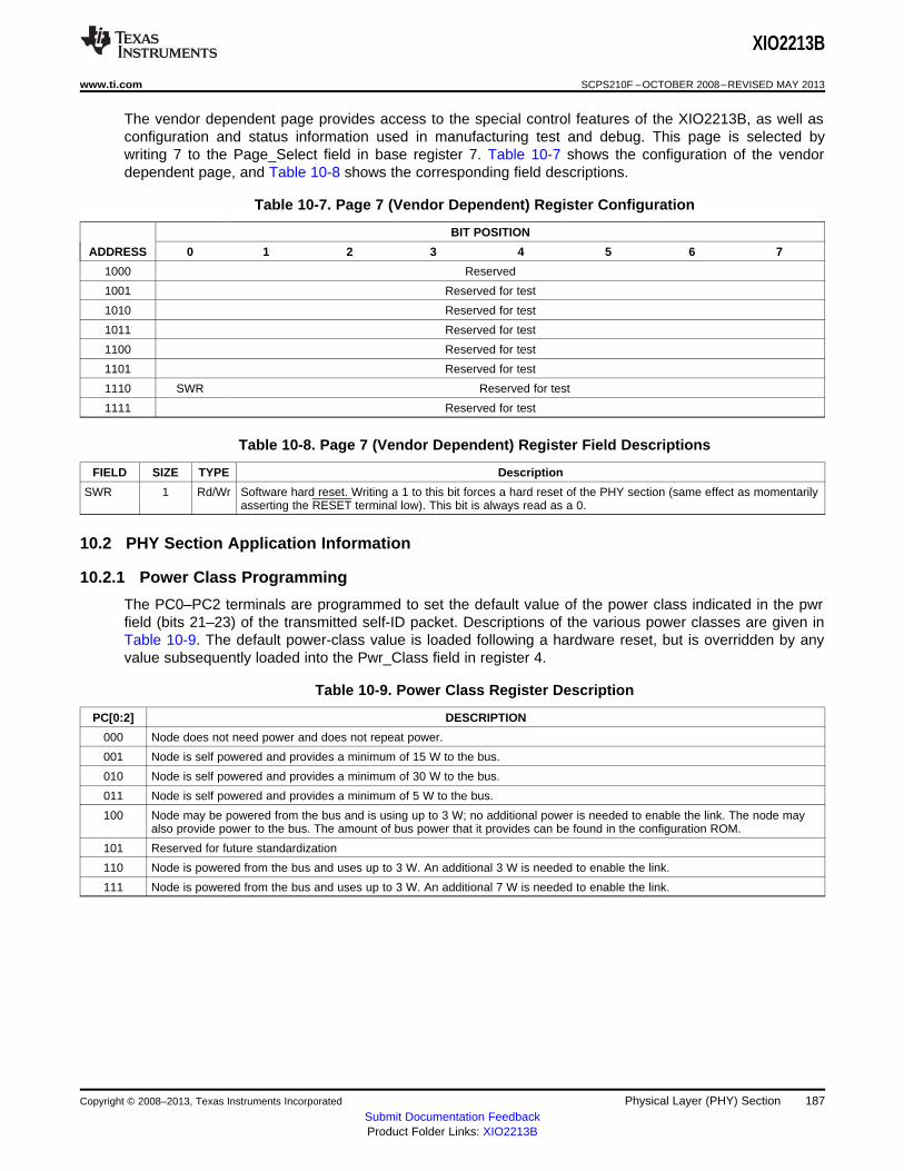
XIO2213B
www.ti.com SCPS210F –OCTOBER 2008–REVISED MAY 2013
The vendor dependent page provides access to the special control features of the XIO2213B, as well asconfiguration and status information used in manufacturing test and debug. This page is selected bywriting 7 to the Page_Select field in base register 7. Table 10-7 shows the configuration of the vendordependent page, and Table 10-8 shows the corresponding field descriptions.
Table 10-7. Page 7 (Vendor Dependent) Register Configuration
BIT POSITION
ADDRESS 0 1 2 3 4 5 6 7
1000 Reserved
1001 Reserved for test
1010 Reserved for test
1011 Reserved for test
1100 Reserved for test
1101 Reserved for test
1110 SWR Reserved for test
1111 Reserved for test
Table 10-8. Page 7 (Vendor Dependent) Register Field Descriptions
FIELD SIZE TYPE Description
SWR 1 Rd/Wr Software hard reset. Writing a 1 to this bit forces a hard reset of the PHY section (same effect as momentarilyasserting the RESET terminal low). This bit is always read as a 0.
10.2 PHY Section Application Information
10.2.1 Power Class Programming
The PC0–PC2 terminals are programmed to set the default value of the power class indicated in the pwrfield (bits 21–23) of the transmitted self-ID packet. Descriptions of the various power classes are given inTable 10-9. The default power-class value is loaded following a hardware reset, but is overridden by anyvalue subsequently loaded into the Pwr_Class field in register 4.
Table 10-9. Power Class Register Description
PC[0:2] DESCRIPTION
000 Node does not need power and does not repeat power.
001 Node is self powered and provides a minimum of 15 W to the bus.
010 Node is self powered and provides a minimum of 30 W to the bus.
011 Node is self powered and provides a minimum of 5 W to the bus.
100 Node may be powered from the bus and is using up to 3 W; no additional power is needed to enable the link. The node mayalso provide power to the bus. The amount of bus power that it provides can be found in the configuration ROM.
101 Reserved for future standardization
110 Node is powered from the bus and uses up to 3 W. An additional 3 W is needed to enable the link.
111 Node is powered from the bus and uses up to 3 W. An additional 7 W is needed to enable the link.
Copyright © 2008–2013, Texas Instruments Incorporated Physical Layer (PHY) Section 187Submit Documentation FeedbackProduct Folder Links: XIO2213B
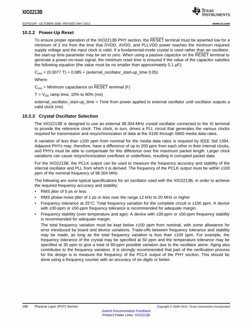
XIO2213B
SCPS210F –OCTOBER 2008–REVISED MAY 2013 www.ti.com
10.2.2 Power-Up Reset
To ensure proper operation of the XIO2213B PHY section, the RESET terminal must be asserted low for aminimum of 2 ms from the time that DVDD, AVDD, and PLLVDD power reaches the minimum requiredsupply voltage and the input clock is valid. If a fundamental-mode crystal is used rather than an oscillator,the start-up time parameter may be set to zero. When using a passive capacitor on the RESET terminal togenerate a power-on-reset signal, the minimum reset time is ensured if the value of the capacitor satisfiesthe following equation (the value must be no smaller than approximately 0.1 μF):
Cmin = (0.0077 T) + 0.085 + (external_oscillator_start-up_time 0.05)
Where:
Cmin = Minimum capacitance on RESET terminal (F)
T = VDD ramp time, 10% to 90% (ms)
external_oscillator_start-up_time = Time from power applied to external oscillator until oscillator outputs avalid clock (ms)
10.2.3 Crystal Oscillator Selection
The XIO2213B is designed to use an external 98.304-MHz crystal oscillator connected to the XI terminalto provide the reference clock. This clock, in turn, drives a PLL circuit that generates the various clocksrequired for transmission and resynchronization of data at the S100 through S800 media data rates.
A variation of less than ±100 ppm from nominal for the media data rates is required by IEEE Std 1394.Adjacent PHYs may, therefore, have a difference of up to 200 ppm from each other in their internal clocks,and PHYs must be able to compensate for this difference over the maximum packet length. Larger clockvariations can cause resynchronization overflows or underflows, resulting in corrupted packet data.
For the XIO2213B, the PCLK output can be used to measure the frequency accuracy and stability of theinternal oscillator and PLL from which it is derived. The frequency of the PCLK output must be within ±100ppm of the nominal frequency of 98.304 MHz.
The following are some typical specifications for an oscillator used with the XIO2213B, in order to achievethe required frequency accuracy and stability:• RMS jitter of 5 ps or less• RMS phase-noise jitter of 1 ps or less over the range 12 kHz to 20 MHz or higher• Frequency tolerance at 25°C: Total frequency variation for the complete circuit is ±100 ppm. A device
with ±30-ppm or ±50-ppm frequency tolerance is recommended for adequate margin.• Frequency stability (over temperature and age): A device with ±30-ppm or ±50-ppm frequency stability
is recommended for adequate margin.The total frequency variation must be kept below ±100 ppm from nominal, with some allowance forerror introduced by board and device variations. Trade-offs between frequency tolerance and stabilitymay be made, as long as the total frequency variation is less than ±100 ppm. For example, thefrequency tolerance of the crystal may be specified at 50 ppm and the temperature tolerance may bespecified at 30 ppm to give a total of 80-ppm possible variation due to the oscillator alone. Aging alsocontributes to the frequency variation. It is strongly recommended that part of the verification processfor the design is to measure the frequency of the PCLK output of the PHY section. This should bedone using a frequency counter with an accuracy of six digits or better.
188 Physical Layer (PHY) Section Copyright © 2008–2013, Texas Instruments Incorporated
Submit Documentation FeedbackProduct Folder Links: XIO2213B
XIO2213B
www.ti.com SCPS210F –OCTOBER 2008–REVISED MAY 2013
10.2.4 Bus Reset
It is recommended that whenever the user has a choice, the user should initiate a bus reset by writing tothe initiate short bus reset (ISBR) bit (bit 1, PHY register 0101b). Care must be taken not to change thevalue of any of the other writeable bits in this register when the ISBR bit is written to.
In the XIO2213B, the initiate bus reset (IBR) bit can be set to 1 in order to initiate a bus reset andinitialization sequence; however, it is recommended to use the ISBR bit instead. The IBR bit is located inPHY register 1 along with the root holdoff bit (RHB) and gap count. As required by the IEEE Std 1394b-2002 Supplement, this configuration maintains compatibility with older TI PHY designs that were based oneither the suggested register set defined in Annex J of IEEE Std 1394-1995 or the IEEE Std 1394a-2000Supplement. Therefore, whenever the IBR bit is written, the RHB and gap count are also necessarilywritten.
It is recommended that the RHB and gap count only be updated by PHY configuration packets. TheXIO2213B is IEEE Std 1394a-2000 and IEEE Std 1394b-2002 compliant and, therefore, both the receptionand transmission of PHY configuration packets cause the RHB and gap count to be loaded, unlike olderIEEE Std 1394-1995-compliant PHYs that decode only received PHY configuration packets.
The gap count is set to the maximum value of 63 after two consecutive bus resets without an interveningwrite to the gap count, either by a write to PHY register 1 or by a PHY configuration packet. Thismechanism allows a PHY configuration packet to be transmitted and then a bus reset initiated to verifythat all nodes on the bus have updated their RHBs and gap counts, without having the gap count set backto 63 by the bus reset. The subsequent connection of a new node to the bus, which initiates a bus reset,then causes the gap count of each node to be set to 63. Note, however, that if a subsequent bus reset isinstead initiated by a write to register 1 to set the IBR bit, all other nodes on the bus have their gap countsset to 63, while this nodes gap count remains set to the value just loaded by the write to PHY register 1.
Therefore, in order to maintain consistent gap counts throughout the bus, the following rules apply to theuse of the IBR bit, RHB, and gap count in PHY register 1:• Following the transmission of a PHY configuration packet, a bus reset must be initiated in order to
verify that all nodes have correctly updated their RHBs and gap counts, and to ensure that asubsequent new connection to the bus causes the gap count to be set to 63 on all nodes in the bus. Ifthis bus reset is initiated by setting the IBR bit to 1, the RHB and gap count register must also beloaded with the correct values consistent with the just-transmitted PHY configuration packet. In theXIO2213B, the RHB and gap count have been updated to their correct values on the transmission ofthe PHY configuration packet, so these values can first be read from register 1 and then rewritten.
• Other than to initiate the bus reset that must follow the transmission of a PHY configuration packet,when the IBR bit is set to 1 in order to initiate a bus reset, the gap count must also be set to 63 to beconsistent with other nodes on the bus, and the RHB must be maintained with its current value.
• The PHY register 1 must not be written to except to set the IBR bit. The RHB and gap count must notbe written without also setting the IBR bit to 1.
• To avoid these problems, all bus resets initiated by software must be initiated by writing the ISBR bit(bit 1 PHY register 0101b). Care must be taken to not change the value of any of the other writeablebits in this register when the ISBR bit is written to. Also, the only means to change the gap count ofany node must be by means of the PHY configuration packet, which changes all nodes to the samegap count.
Copyright © 2008–2013, Texas Instruments Incorporated Physical Layer (PHY) Section 189Submit Documentation FeedbackProduct Folder Links: XIO2213B
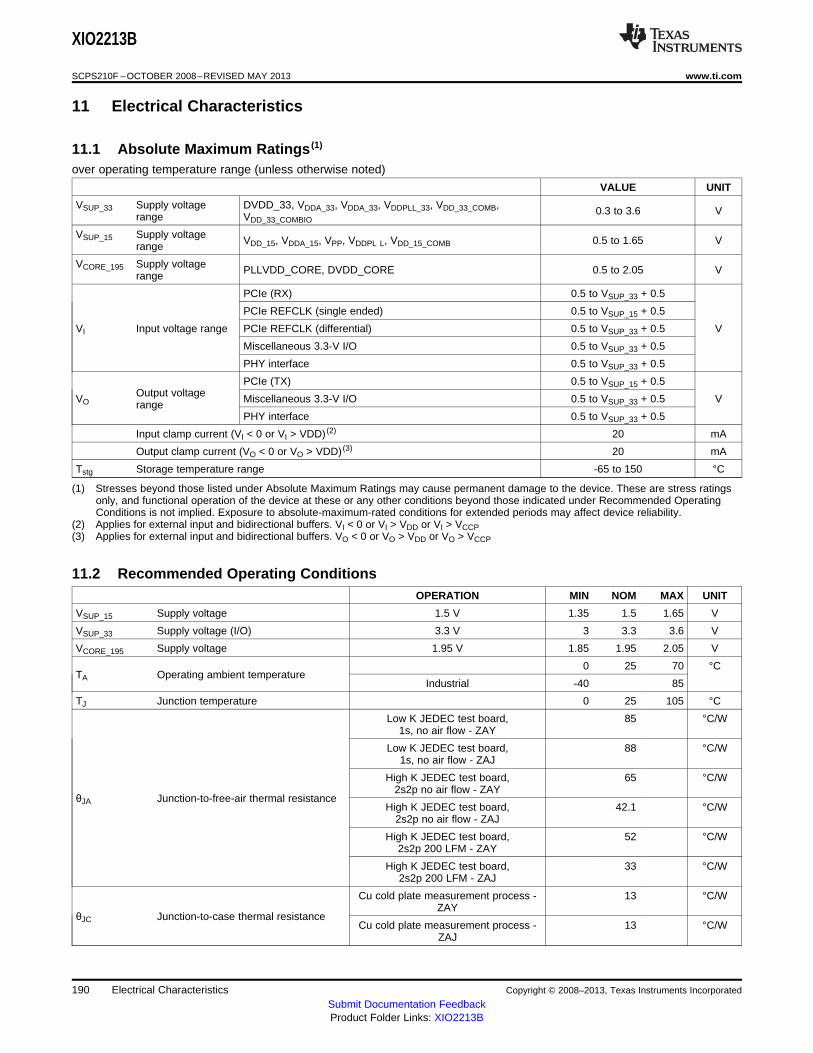
XIO2213B
SCPS210F –OCTOBER 2008–REVISED MAY 2013 www.ti.com
11 Electrical Characteristics
11.1 Absolute Maximum Ratings (1)
over operating temperature range (unless otherwise noted)
VALUE UNIT
VSUP_33 Supply voltage DVDD_33, VDDA_33, VDDA_33, VDDPLL_33, VDD_33_COMB, 0.3 to 3.6 Vrange VDD_33_COMBIO
VSUP_15 Supply voltage VDD_15, VDDA_15, VPP, VDDPL L, VDD_15_COMB 0.5 to 1.65 Vrange
VCORE_195 Supply voltage PLLVDD_CORE, DVDD_CORE 0.5 to 2.05 Vrange
PCIe (RX) 0.5 to VSUP_33 + 0.5
PCIe REFCLK (single ended) 0.5 to VSUP_15 + 0.5
VI Input voltage range PCIe REFCLK (differential) 0.5 to VSUP_33 + 0.5 V
Miscellaneous 3.3-V I/O 0.5 to VSUP_33 + 0.5
PHY interface 0.5 to VSUP_33 + 0.5
PCIe (TX) 0.5 to VSUP_15 + 0.5Output voltageVO Miscellaneous 3.3-V I/O 0.5 to VSUP_33 + 0.5 Vrange
PHY interface 0.5 to VSUP_33 + 0.5
Input clamp current (VI < 0 or VI > VDD) (2) 20 mA
Output clamp current (VO < 0 or VO > VDD) (3) 20 mA
Tstg Storage temperature range -65 to 150 °C
(1) Stresses beyond those listed under Absolute Maximum Ratings may cause permanent damage to the device. These are stress ratingsonly, and functional operation of the device at these or any other conditions beyond those indicated under Recommended OperatingConditions is not implied. Exposure to absolute-maximum-rated conditions for extended periods may affect device reliability.
(2) Applies for external input and bidirectional buffers. VI < 0 or VI > VDD or VI > VCCP(3) Applies for external input and bidirectional buffers. VO < 0 or VO > VDD or VO > VCCP
11.2 Recommended Operating ConditionsOPERATION MIN NOM MAX UNIT
VSUP_15 Supply voltage 1.5 V 1.35 1.5 1.65 V
VSUP_33 Supply voltage (I/O) 3.3 V 3 3.3 3.6 V
VCORE_195 Supply voltage 1.95 V 1.85 1.95 2.05 V
0 25 70 °CTA Operating ambient temperature
Industrial -40 85
TJ Junction temperature 0 25 105 °C
Low K JEDEC test board, 85 °C/W1s, no air flow - ZAY
Low K JEDEC test board, 88 °C/W1s, no air flow - ZAJ
High K JEDEC test board, 65 °C/W2s2p no air flow - ZAY
θJA Junction-to-free-air thermal resistanceHigh K JEDEC test board, 42.1 °C/W
2s2p no air flow - ZAJ
High K JEDEC test board, 52 °C/W2s2p 200 LFM - ZAY
High K JEDEC test board, 33 °C/W2s2p 200 LFM - ZAJ
Cu cold plate measurement process - 13 °C/WZAY
θJC Junction-to-case thermal resistanceCu cold plate measurement process - 13 °C/W
ZAJ
190 Electrical Characteristics Copyright © 2008–2013, Texas Instruments Incorporated
Submit Documentation FeedbackProduct Folder Links: XIO2213B
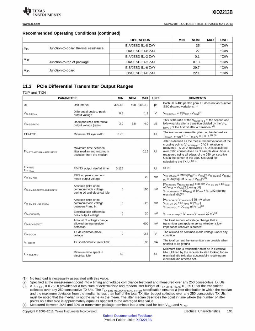
XIO2213B
www.ti.com SCPS210F –OCTOBER 2008–REVISED MAY 2013
Recommended Operating Conditions (continued)
OPERATION MIN NOM MAX UNIT
EIA/JESD 51-8 ZAY 35 °C/WθJB Junction-to-board thermal resistance
EIA/JESD 51-8 ZAJ 27 °C/W
EIA/JESD 51-2 ZAY 0.1 °C/WΨJT
Junction-to-top of package EIA/JESD 51-2 ZAJ 0.13 °C/W
EIS/JESD 51-6 ZAY 29.7 °C/WΨJB Junction-to-board
EIS/JESD 51-6 ZAJ 22.1 °C/W
11.3 PCIe Differential Transmitter Output RangesTXP and TXN
PARAMETER MIN NOM MAX UNIT COMMENTS
Each UI is 400 ps 300 ppm. UI does not account forUI Unit interval 399.88 400 400.12 ps SSC dictated variations. (1)
Differential peak-to-peakVTX-DIFFp-p 0.8 1.2 V VTX-DIFFp-p = 2*|VTXP - VTXN| (2)output voltage
This is the ratio of the VTX-DIFFp-p of the second andDeemphasized differential following bits after a transition divided by the VTX-VTX-DE-RATIO 3.0 3.5 4.0 dBoutput voltage (ratio)
DIFFp-p of the first bit after a transition. (2)
The maximum transmitter jitter can be derived asTTX-EYE Minimum TX eye width 0.75 UI
TTXMAX- JITTER = 1 – TTX-EYE = 0.3 UI.(2) (3)
Jitter is defined as the measurement variation of thecrossing points (VTX-DIFFp-p = 0 V) in relation torecovered TX UI. A recovered TX UI is calculatedMaximum time betweenover 3500 consecutive UIs of sample data. Jitter isTTX-EYE-MEDIAN-to-MAX-JITTER jitter median and maximum 0.15 UImeasured using all edges of the 250 consecutivedeviation from the medianUIs in the center of the 3500 UIs used forcalculating the TX UI.(2) (3)
TTX-RISE P/N TX output rise/fall time 0.125 UI (2) (4)TTX-FALL
VTX-CM-ACp = RMS(|VTXP + VTXN|/2 VTX-CM-DC) VTX-CM-RMS ac peak common-VTX-CM-ACp 20 mVmode output voltage DC = DC(avg) of |VTXP + VTXN|/2(2)
|VTX-CM-DC VTX-CM-Idle-DC| 100 mV VTX-CM-DC = DC(avg)Absolute delta of dc of |VTXP + VTXN|/2 [during L0]VTX-CM-DC-ACTIVE-IDLE-DELTA common-mode voltage 0 100 mV VTX-CM-Idle-DC = DC(avg) of |VTXP + VTXN|/2 (during
during L0 and electrical idleelectrical idle)(2)
|VTXP-CM-DC VTXN-CM-DC| 25 mV whenAbsolute delta of dcVTXP-CM-DC = DC(avg) of |VTXP|VTX-CM-DC-LINE-DELTA common-mode voltage 0 25 mV
between P and N VTXN-CM-DC = DC(avg) of |VTXN|(2)
Electrical idle differentialVTX-IDLE-DIFFp 0 20 mV VTX-IDLE-DIFFp = |VTXP-Idle VTXN-Idle| 20 mV(2)peak output voltage
Amount of voltage change The total amount of voltage change that aVTX-RCV-DETECT allowed during receiver 600 mV transmitter can apply to sense whether a low
detection impedance receiver is present
TX dc common-mode The allowed dc common-mode voltage under anyVTX-DC-CM 0 3.6 Vvoltage condition
The total current the transmitter can provide whenITX-SHORT TX short-circuit current limit 90 mA shorted to its ground
Minimum time a transmitter must be in electricalMinimum time spent in Idle. Utilized by the receiver to start looking for anTTX-IDLE-MIN 50 UIelectrical idle electrical idle exit after successfully receiving an
electrical idle ordered set.
(1) No test load is necessarily associated with this value.(2) Specified at the measurement point into a timing and voltage compliance test load and measured over any 250 consecutive TX UIs.(3) A TTX-EYE = 0.75 UI provides for a total sum of deterministic and random jitter budget of TTX-JITTER-MAX = 0.25 UI for the transmitter
collected over any 250 consecutive TX UIs. The TTX-EYE-MEDIAN-to-MAX-JITTER specification ensures a jitter distribution in which the medianand the maximum deviation from the median is less than half of the total TX jitter budget collected over any 250 consecutive TX UIs. Itmust be noted that the median is not the same as the mean. The jitter median describes the point in time where the number of jitterpoints on either side is approximately equal as opposed to the averaged time value.
(4) Measured between 20% and 80% at transmitter package terminals into a test load for both VTXP and VTXN.
Copyright © 2008–2013, Texas Instruments Incorporated Electrical Characteristics 191Submit Documentation FeedbackProduct Folder Links: XIO2213B
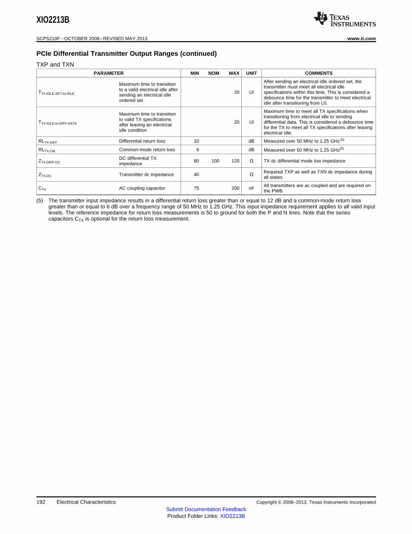
XIO2213B
SCPS210F –OCTOBER 2008–REVISED MAY 2013 www.ti.com
PCIe Differential Transmitter Output Ranges (continued)
TXP and TXNPARAMETER MIN NOM MAX UNIT COMMENTS
After sending an electrical idle ordered set, theMaximum time to transition transmitter must meet all electrical idleto a valid electrical idle afterTTX-IDLE-SET-to-IDLE 20 UI specifications within this time. This is considered asending an electrical idle debounce time for the transmitter to meet electricalordered set idle after transitioning from L0.
Maximum time to meet all TX specifications whenMaximum time to transition transitioning from electrical idle to sendingto valid TX specificationsTTX-IDLE-to-DIFF-DATA 20 UI differential data. This is considered a debounce timeafter leaving an electrical for the TX to meet all TX specifications after leavingidle condition electrical idle.
RLTX-DIFF Differential return loss 10 dB Measured over 50 MHz to 1.25 GHz (5)
RLTX-CM Common-mode return loss 6 dB Measured over 50 MHz to 1.25 GHz(5)
DC differential TXZTX-DIFF-DC 80 100 120 Ω TX dc differential mode low impedanceimpedance
Required TXP as well as TXN dc impedance duringZTX-DC Transmitter dc impedance 40 Ω all states
All transmitters are ac coupled and are required onCTX AC coupling capacitor 75 200 nF the PWB.
(5) The transmitter input impedance results in a differential return loss greater than or equal to 12 dB and a common-mode return lossgreater than or equal to 6 dB over a frequency range of 50 MHz to 1.25 GHz. This input impedance requirement applies to all valid inputlevels. The reference impedance for return loss measurements is 50 to ground for both the P and N lines. Note that the seriescapacitors CTX is optional for the return loss measurement.
192 Electrical Characteristics Copyright © 2008–2013, Texas Instruments Incorporated
Submit Documentation FeedbackProduct Folder Links: XIO2213B
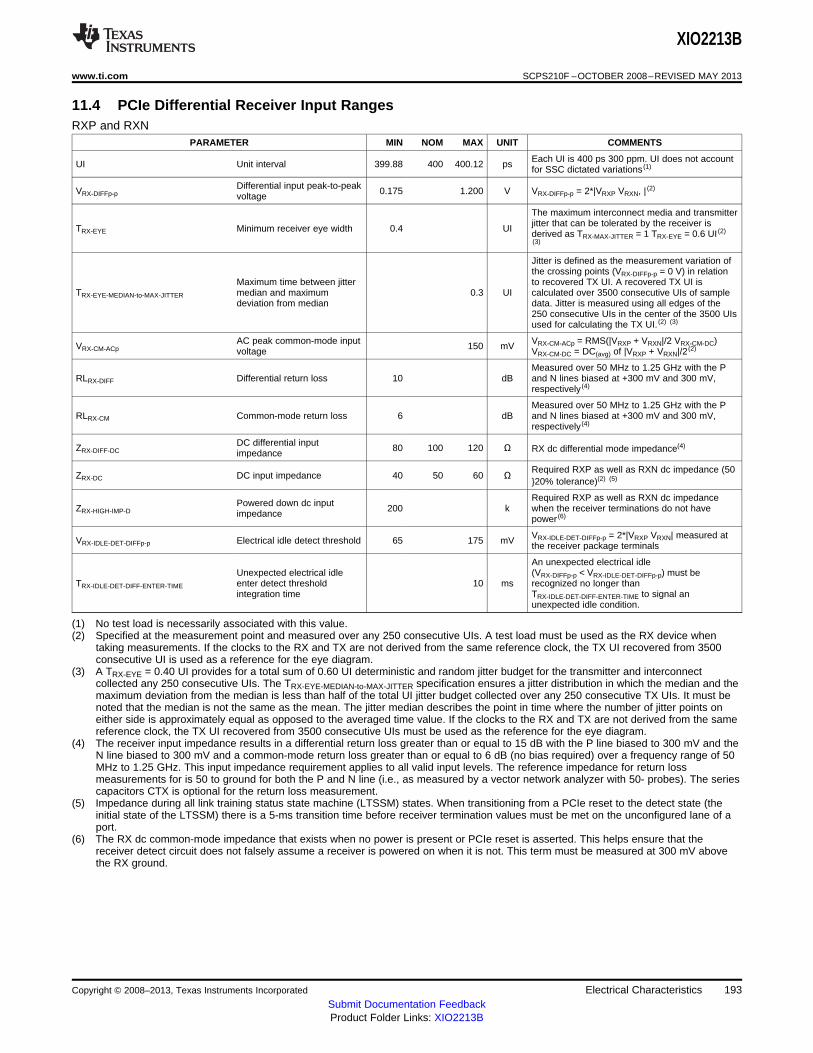
XIO2213B
www.ti.com SCPS210F –OCTOBER 2008–REVISED MAY 2013
11.4 PCIe Differential Receiver Input RangesRXP and RXN
PARAMETER MIN NOM MAX UNIT COMMENTS
Each UI is 400 ps 300 ppm. UI does not accountUI Unit interval 399.88 400 400.12 ps for SSC dictated variations (1)
Differential input peak-to-peakVRX-DIFFp-p 0.175 1.200 V VRX-DIFFp-p = 2*|VRXP VRXN, | (2)voltage
The maximum interconnect media and transmitterjitter that can be tolerated by the receiver isTRX-EYE Minimum receiver eye width 0.4 UI derived as TRX-MAX-JITTER = 1 TRX-EYE = 0.6 UI (2)
(3)
Jitter is defined as the measurement variation ofthe crossing points (VRX-DIFFp-p = 0 V) in relation
Maximum time between jitter to recovered TX UI. A recovered TX UI isTRX-EYE-MEDIAN-to-MAX-JITTER median and maximum 0.3 UI calculated over 3500 consecutive UIs of sample
deviation from median data. Jitter is measured using all edges of the250 consecutive UIs in the center of the 3500 UIsused for calculating the TX UI. (2) (3)
AC peak common-mode input VRX-CM-ACp = RMS(|VRXP + VRXN|/2 VRX-CM-DC)VRX-CM-ACp 150 mVvoltage VRX-CM-DC = DC(avg) of |VRXP + VRXN|/2(2)
Measured over 50 MHz to 1.25 GHz with the PRLRX-DIFF Differential return loss 10 dB and N lines biased at +300 mV and 300 mV,
respectively (4)
Measured over 50 MHz to 1.25 GHz with the PRLRX-CM Common-mode return loss 6 dB and N lines biased at +300 mV and 300 mV,
respectively (4)
DC differential inputZRX-DIFF-DC 80 100 120 Ω RX dc differential mode impedance(4)impedance
Required RXP as well as RXN dc impedance (50ZRX-DC DC input impedance 40 50 60 Ω
20% tolerance)(2) (5)
Required RXP as well as RXN dc impedancePowered down dc inputZRX-HIGH-IMP-D 200 k when the receiver terminations do not haveimpedance power (6)
VRX-IDLE-DET-DIFFp-p = 2*|VRXP VRXN| measured atVRX-IDLE-DET-DIFFp-p Electrical idle detect threshold 65 175 mV the receiver package terminals
An unexpected electrical idleUnexpected electrical idle (VRX-DIFFp-p < VRX-IDLE-DET-DIFFp-p) must be
TRX-IDLE-DET-DIFF-ENTER-TIME enter detect threshold 10 ms recognized no longer thanintegration time TRX-IDLE-DET-DIFF-ENTER-TIME to signal an
unexpected idle condition.
(1) No test load is necessarily associated with this value.(2) Specified at the measurement point and measured over any 250 consecutive UIs. A test load must be used as the RX device when
taking measurements. If the clocks to the RX and TX are not derived from the same reference clock, the TX UI recovered from 3500consecutive UI is used as a reference for the eye diagram.
(3) A TRX-EYE = 0.40 UI provides for a total sum of 0.60 UI deterministic and random jitter budget for the transmitter and interconnectcollected any 250 consecutive UIs. The TRX-EYE-MEDIAN-to-MAX-JITTER specification ensures a jitter distribution in which the median and themaximum deviation from the median is less than half of the total UI jitter budget collected over any 250 consecutive TX UIs. It must benoted that the median is not the same as the mean. The jitter median describes the point in time where the number of jitter points oneither side is approximately equal as opposed to the averaged time value. If the clocks to the RX and TX are not derived from the samereference clock, the TX UI recovered from 3500 consecutive UIs must be used as the reference for the eye diagram.
(4) The receiver input impedance results in a differential return loss greater than or equal to 15 dB with the P line biased to 300 mV and theN line biased to 300 mV and a common-mode return loss greater than or equal to 6 dB (no bias required) over a frequency range of 50MHz to 1.25 GHz. This input impedance requirement applies to all valid input levels. The reference impedance for return lossmeasurements for is 50 to ground for both the P and N line (i.e., as measured by a vector network analyzer with 50- probes). The seriescapacitors CTX is optional for the return loss measurement.
(5) Impedance during all link training status state machine (LTSSM) states. When transitioning from a PCIe reset to the detect state (theinitial state of the LTSSM) there is a 5-ms transition time before receiver termination values must be met on the unconfigured lane of aport.
(6) The RX dc common-mode impedance that exists when no power is present or PCIe reset is asserted. This helps ensure that thereceiver detect circuit does not falsely assume a receiver is powered on when it is not. This term must be measured at 300 mV abovethe RX ground.
Copyright © 2008–2013, Texas Instruments Incorporated Electrical Characteristics 193Submit Documentation FeedbackProduct Folder Links: XIO2213B
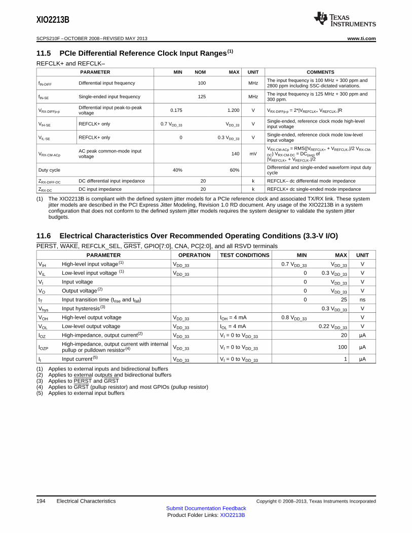
XIO2213B
SCPS210F –OCTOBER 2008–REVISED MAY 2013 www.ti.com
11.5 PCIe Differential Reference Clock Input Ranges (1)
REFCLK+ and REFCLK–PARAMETER MIN NOM MAX UNIT COMMENTS
The input frequency is 100 MHz + 300 ppm andfIN-DIFF Differential input frequency 100 MHz 2800 ppm including SSC-dictated variations.
The input frequency is 125 MHz + 300 ppm andfIN-SE Single-ended input frequency 125 MHz 300 ppm.
Differential input peak-to-peakVRX-DIFFp-p 0.175 1.200 V VRX-DIFFp-p = 2*|VREFCLK+ VREFCLK–|Rvoltage
Single-ended, reference clock mode high-levelVIH-SE REFCLK+ only 0.7 VDD_33 VDD_33 V input voltage
Single-ended, reference clock mode low-levelVIL-SE REFCLK+ only 0 0.3 VDD_33 V input voltage
VRX-CM-ACp = RMS(|VREFCLK+ + VREFCLK–|/2 VRX-CM-AC peak common-mode inputVRX-CM-ACp 140 mV DC) VRX-CM-DC = DC(avg) ofvoltage |VREFCLK+ + VREFCLK–|/2
Differential and single-ended waveform input dutyDuty cycle 40% 60% cycle
ZRX-DIFF-DC DC differential input impedance 20 k REFCLK– dc differential mode impedance
ZRX-DC DC input impedance 20 k REFCLK+ dc single-ended mode impedance
(1) The XIO2213B is compliant with the defined system jitter models for a PCIe reference clock and associated TX/RX link. These systemjitter models are described in the PCI Express Jitter Modeling, Revision 1.0 RD document. Any usage of the XIO2213B in a systemconfiguration that does not conform to the defined system jitter models requires the system designer to validate the system jitterbudgets.
11.6 Electrical Characteristics Over Recommended Operating Conditions (3.3-V I/O)PERST, WAKE, REFCLK_SEL, GRST, GPIO[7:0], CNA, PC[2:0], and all RSVD terminals
PARAMETER OPERATION TEST CONDITIONS MIN MAX UNIT
VIH High-level input voltage (1) VDD_33 0.7 VDD_33 VDD_33 V
VIL Low-level input voltage (1) VDD_33 0 0.3 VDD_33 V
VI Input voltage 0 VDD_33 V
VO Output voltage (2) 0 VDD_33 V
tT Input transition time (trise and tfall) 0 25 ns
Vhys Input hysteresis (3) 0.3 VDD_33 V
VOH High-level output voltage VDD_33 IOH = 4 mA 0.8 VDD_33 V
VOL Low-level output voltage VDD_33 IOL = 4 mA 0.22 VDD_33 V
IOZ High-impedance, output current(2) VDD_33 VI = 0 to VDD_33 20 μA
High-impedance, output current with internalIOZP VDD_33 VI = 0 to VDD_33 100 μApullup or pulldown resistor (4)
II Input current (5) VDD_33 VI = 0 to VDD_33 1 μA
(1) Applies to external inputs and bidirectional buffers(2) Applies to external outputs and bidirectional buffers(3) Applies to PERST and GRST(4) Applies to GRST (pullup resistor) and most GPIOs (pullup resistor)(5) Applies to external input buffers
194 Electrical Characteristics Copyright © 2008–2013, Texas Instruments Incorporated
Submit Documentation FeedbackProduct Folder Links: XIO2213B
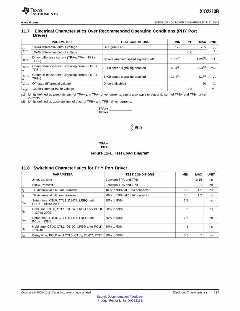
TPAx+
TPBx+
TPAx-
TPBx-
56 W
XIO2213B
www.ti.com SCPS210F –OCTOBER 2008–REVISED MAY 2013
11.7 Electrical Characteristics Over Recommended Operating Conditions (PHY PortDriver)
PARAMETER TEST CONDITIONS MIN TYP MAX UNIT
1394a differential output voltage 56 Figure 11-1 172 265VOD mV
1394b differential output voltage 700
Driver difference current (TPA+, TPA–, TPB+,IDIFF Drivers enabled, speed signaling off 1.05 (1) 1.05 (1) mATPB–)
ISP20 Common-mode speed signaling current (TPB+, S200 speed signaling enabled 4.84 (2) 2.53 (2) mA0 TPB–)
ISP40 Common-mode speed signaling current (TPB+, S400 speed signaling enabled 12.4 (2) 8.1 (2) mA0 TPB–)
VOFF Off-state differential voltage Drivers disabled 20 mV
VCM 1394b common-mode voltage 1.5 V
(1) Limits defined as algebraic sum of TPA+ and TPA– driver currents. Limits also apply to algebraic sum of TPB+ and TPB– drivercurrents.
(2) Limits defined as absolute limit of each of TPB+ and TPB– driver currents.
Figure 11-1. Test Load Diagram
11.8 Switching Characteristics for PHY Port DriverPARAMETER TEST CONDITIONS MIN MAX UNIT
Jitter, transmit Between TPA and TPB 0.15 ns
Skew, transmit Between TPA and TPB 0.1 ns
tr TP differential rise time, transmit 10% to 90%, at 1394 connector 0.5 1.2 ns
tf TP differential fall time, transmit 90% to 10%, at 1394 connector 0.5 1.2 ns
Setup time, CTL0, CTL1, D1-D7, LREQ until 50% to 50% 2.5 nstsu PCLK - 1394a-2000
Hold time, CTL0, CTL1, D1-D7, LREQ after PCLK 50% to 50% 0 nsth - 1394a-2000
Setup time, CTL0, CTL1, D1-D7, LREQ until 50% to 50% 2.5 nstsu PCLK - 1394b
Hold time, CTL0, CTL1, D1-D7, LREQ after PCLK 50% to 50% 1 nsth - 1394b
td Delay time, PCLK until CTL0, CTL1, D1-D7, PINT 50% to 50% 0.5 7 ns
Copyright © 2008–2013, Texas Instruments Incorporated Electrical Characteristics 195Submit Documentation FeedbackProduct Folder Links: XIO2213B
XIO2213B
SCPS210F –OCTOBER 2008–REVISED MAY 2013 www.ti.com
11.9 Electrical Characteristics Over Recommended Operating Conditions PHY PortReceiver
PARAMETER TEST CONDITIONS MIN TYP MAX UNIT
4 7 kZID Differential impedance Drivers disabled
4 pF
20 kZIC Common-mode impedance Drivers disabled
24 pF
VTH-R Receiver input threshold voltage Drivers disabled 30 30 mV
Cable bias detect threshold. TPBxVTH-CB Drivers disabled 0.6 1 Vcable inputs
Positive arbitration comparatorVTH+ Drivers disabled 89 168 mVthreshold voltage
Negative arbitration comparatorVTH Drivers disabled 168 89 mVthreshold voltage
VTH-SP200 Speed signal threshold TPBIAS-TPA common mode voltage, drivers disabled 49 131 mV
VTH-SP400 Speed signal threshold TPBIAS-TPA common mode voltage, drivers disabled 314 396 mV
11.10 Jitter/Skew Characteristics for 1394a PHY Port ReceiverPARAMETER MIN TYP MAX UNIT
TPA, TPB cable inputs, S100 operation 1.08
1394a Receive input jitter TPA, TPB cable inputs, S200 operation 0.5 ns
TPA, TPB cable inputs, S400 operation 0.315
Between TPA and TPB cable inputs, S100 operation 0.8
1394a Receive input skew Between TPA and TPB cable inputs, S200 operation 0.55 ns
Between TPA and TPB cable inputs, S400 operation 0.5
11.11 Operating, Timing, and Switching Characteristics of XIPARAMETER MIN TYP MAX UNIT
VIH High-level input voltage 0.63 VDDA_15 V
VIL Low-level input voltage 0.33 VDDA_15 V
Input clock frequency 98.304 MHz
Input clock frequency tolerance <100 ppm
Input slew rate 0.2 4 V/ns
Input clock duty cycle 40% 60%
11.12 Electrical Characteristics Over Recommended Operating Conditions(1394a Miscellaneous I/O)
PARAMETER TEST CONDITIONS MIN MAX UNIT
VTH Power status threshold CPS input (1) 400-kΩ resistor (1) 4.7 7.5 V
VO TPBIAS output voltage At rated IO current 1.665 2.015 V
IO TPBIAS output current 5.6 1.3 mA
(1) Measure at cable power side of resistor
12 Glossary
ACRONYM DEFINITION
BIST Built-in self test
ECRC End-to-end cyclic redundancy code
EEPROM Electrically erasable programmable read-only memory
196 Glossary Copyright © 2008–2013, Texas Instruments Incorporated
Submit Documentation FeedbackProduct Folder Links: XIO2213B
XIO2213B
www.ti.com SCPS210F –OCTOBER 2008–REVISED MAY 2013
GP General purpose
GPIO General-purpose input/output
ID Identification
IF Interface
IO Input/output
I2S Inter IC sound
LPM Link power management
LSB Least significant bit
MSB Most significant bit
MSI Message signaled interrupts
PCI Peripheral component interface
PME PCI power-management event
QoS Quality of service
RX Receive
SCL Serial-bus clock
SDA Serial-bus data
TC Traffic class
TLP Transaction layer packet or protocol
TX Transmit
VC Virtual channel
WRR Weighted round-robin
Copyright © 2008–2013, Texas Instruments Incorporated Glossary 197Submit Documentation FeedbackProduct Folder Links: XIO2213B
PACKAGE OPTION ADDENDUM
www.ti.com 5-May-2013
Addendum-Page 1
PACKAGING INFORMATION
Orderable Device Status(1)
Package Type PackageDrawing
Pins PackageQty
Eco Plan(2)
Lead/Ball Finish MSL Peak Temp(3)
Op Temp (°C) Top-Side Markings(4)
Samples
XIO2213BIZAY ACTIVE NFBGA ZAY 167 160 Green (RoHS& no Sb/Br)
SNAGCU Level-3-260C-168 HR -40 to 85 XIO2213BIZAY
XIO2213BZAJ ACTIVE NFBGA ZAJ 168 260 Green (RoHS& no Sb/Br)
SNAGCU Level-3-260C-168 HR 0 to 70 XIO2213B
XIO2213BZAY ACTIVE NFBGA ZAY 167 160 Green (RoHS& no Sb/Br)
SNAGCU Level-3-260C-168 HR 0 to 70 XIO2213BZAY
(1) The marketing status values are defined as follows:ACTIVE: Product device recommended for new designs.LIFEBUY: TI has announced that the device will be discontinued, and a lifetime-buy period is in effect.NRND: Not recommended for new designs. Device is in production to support existing customers, but TI does not recommend using this part in a new design.PREVIEW: Device has been announced but is not in production. Samples may or may not be available.OBSOLETE: TI has discontinued the production of the device.
(2) Eco Plan - The planned eco-friendly classification: Pb-Free (RoHS), Pb-Free (RoHS Exempt), or Green (RoHS & no Sb/Br) - please check http://www.ti.com/productcontent for the latest availabilityinformation and additional product content details.TBD: The Pb-Free/Green conversion plan has not been defined.Pb-Free (RoHS): TI's terms "Lead-Free" or "Pb-Free" mean semiconductor products that are compatible with the current RoHS requirements for all 6 substances, including the requirement thatlead not exceed 0.1% by weight in homogeneous materials. Where designed to be soldered at high temperatures, TI Pb-Free products are suitable for use in specified lead-free processes.Pb-Free (RoHS Exempt): This component has a RoHS exemption for either 1) lead-based flip-chip solder bumps used between the die and package, or 2) lead-based die adhesive used betweenthe die and leadframe. The component is otherwise considered Pb-Free (RoHS compatible) as defined above.Green (RoHS & no Sb/Br): TI defines "Green" to mean Pb-Free (RoHS compatible), and free of Bromine (Br) and Antimony (Sb) based flame retardants (Br or Sb do not exceed 0.1% by weightin homogeneous material)
(3) MSL, Peak Temp. -- The Moisture Sensitivity Level rating according to the JEDEC industry standard classifications, and peak solder temperature.
(4) Multiple Top-Side Markings will be inside parentheses. Only one Top-Side Marking contained in parentheses and separated by a "~" will appear on a device. If a line is indented then it is acontinuation of the previous line and the two combined represent the entire Top-Side Marking for that device.
Important Information and Disclaimer:The information provided on this page represents TI's knowledge and belief as of the date that it is provided. TI bases its knowledge and belief on informationprovided by third parties, and makes no representation or warranty as to the accuracy of such information. Efforts are underway to better integrate information from third parties. TI has taken andcontinues to take reasonable steps to provide representative and accurate information but may not have conducted destructive testing or chemical analysis on incoming materials and chemicals.TI and TI suppliers consider certain information to be proprietary, and thus CAS numbers and other limited information may not be available for release.
In no event shall TI's liability arising out of such information exceed the total purchase price of the TI part(s) at issue in this document sold by TI to Customer on an annual basis.
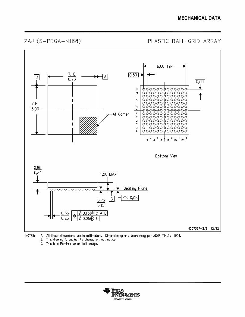
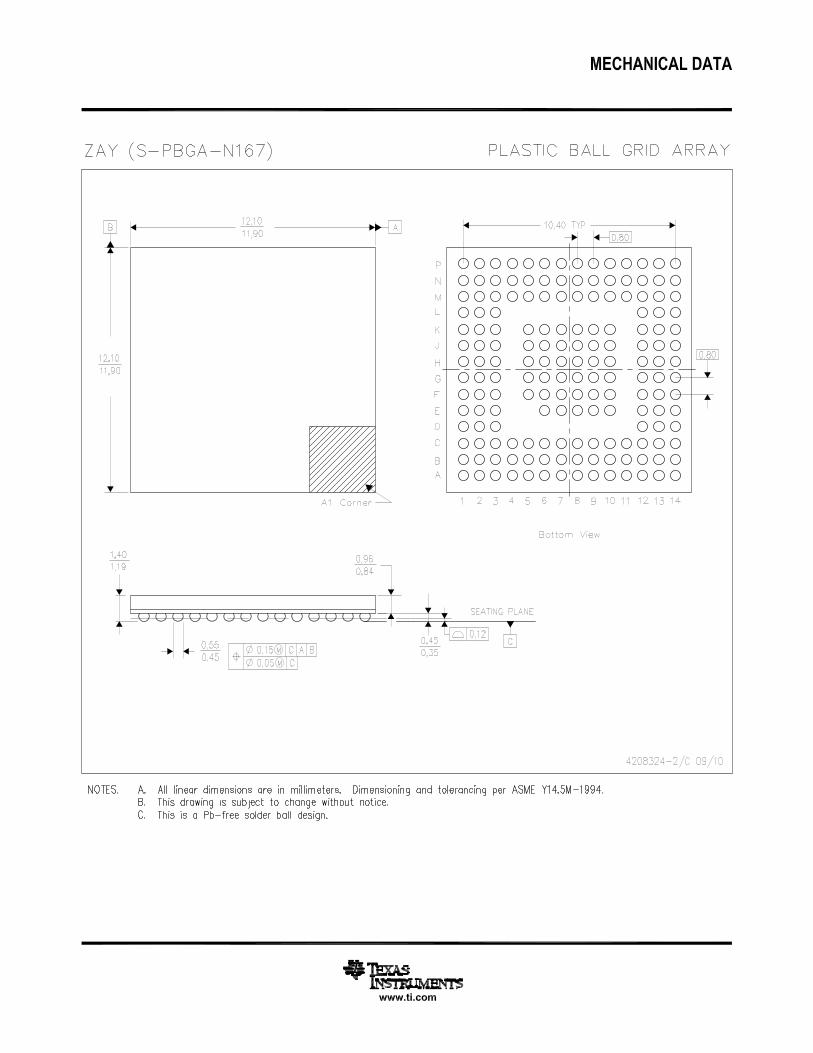

IMPORTANT NOTICE
Texas Instruments Incorporated and its subsidiaries (TI) reserve the right to make corrections, enhancements, improvements and otherchanges to its semiconductor products and services per JESD46, latest issue, and to discontinue any product or service per JESD48, latestissue. Buyers should obtain the latest relevant information before placing orders and should verify that such information is current andcomplete. All semiconductor products (also referred to herein as “components”) are sold subject to TI’s terms and conditions of salesupplied at the time of order acknowledgment.
TI warrants performance of its components to the specifications applicable at the time of sale, in accordance with the warranty in TI’s termsand conditions of sale of semiconductor products. Testing and other quality control techniques are used to the extent TI deems necessaryto support this warranty. Except where mandated by applicable law, testing of all parameters of each component is not necessarilyperformed.
TI assumes no liability for applications assistance or the design of Buyers’ products. Buyers are responsible for their products andapplications using TI components. To minimize the risks associated with Buyers’ products and applications, Buyers should provideadequate design and operating safeguards.
TI does not warrant or represent that any license, either express or implied, is granted under any patent right, copyright, mask work right, orother intellectual property right relating to any combination, machine, or process in which TI components or services are used. Informationpublished by TI regarding third-party products or services does not constitute a license to use such products or services or a warranty orendorsement thereof. Use of such information may require a license from a third party under the patents or other intellectual property of thethird party, or a license from TI under the patents or other intellectual property of TI.
Reproduction of significant portions of TI information in TI data books or data sheets is permissible only if reproduction is without alterationand is accompanied by all associated warranties, conditions, limitations, and notices. TI is not responsible or liable for such altereddocumentation. Information of third parties may be subject to additional restrictions.
Resale of TI components or services with statements different from or beyond the parameters stated by TI for that component or servicevoids all express and any implied warranties for the associated TI component or service and is an unfair and deceptive business practice.TI is not responsible or liable for any such statements.
Buyer acknowledges and agrees that it is solely responsible for compliance with all legal, regulatory and safety-related requirementsconcerning its products, and any use of TI components in its applications, notwithstanding any applications-related information or supportthat may be provided by TI. Buyer represents and agrees that it has all the necessary expertise to create and implement safeguards whichanticipate dangerous consequences of failures, monitor failures and their consequences, lessen the likelihood of failures that might causeharm and take appropriate remedial actions. Buyer will fully indemnify TI and its representatives against any damages arising out of the useof any TI components in safety-critical applications.
In some cases, TI components may be promoted specifically to facilitate safety-related applications. With such components, TI’s goal is tohelp enable customers to design and create their own end-product solutions that meet applicable functional safety standards andrequirements. Nonetheless, such components are subject to these terms.
No TI components are authorized for use in FDA Class III (or similar life-critical medical equipment) unless authorized officers of the partieshave executed a special agreement specifically governing such use.
Only those TI components which TI has specifically designated as military grade or “enhanced plastic” are designed and intended for use inmilitary/aerospace applications or environments. Buyer acknowledges and agrees that any military or aerospace use of TI componentswhich have not been so designated is solely at the Buyer's risk, and that Buyer is solely responsible for compliance with all legal andregulatory requirements in connection with such use.
TI has specifically designated certain components as meeting ISO/TS16949 requirements, mainly for automotive use. In any case of use ofnon-designated products, TI will not be responsible for any failure to meet ISO/TS16949.
Products Applications
Audio www.ti.com/audio Automotive and Transportation www.ti.com/automotive
Amplifiers amplifier.ti.com Communications and Telecom www.ti.com/communications
Data Converters dataconverter.ti.com Computers and Peripherals www.ti.com/computers
DLP® Products www.dlp.com Consumer Electronics www.ti.com/consumer-apps
DSP dsp.ti.com Energy and Lighting www.ti.com/energy
Clocks and Timers www.ti.com/clocks Industrial www.ti.com/industrial
Interface interface.ti.com Medical www.ti.com/medical
Logic logic.ti.com Security www.ti.com/security
Power Mgmt power.ti.com Space, Avionics and Defense www.ti.com/space-avionics-defense
Microcontrollers microcontroller.ti.com Video and Imaging www.ti.com/video
RFID www.ti-rfid.com
OMAP Applications Processors www.ti.com/omap TI E2E Community e2e.ti.com
Wireless Connectivity www.ti.com/wirelessconnectivity
Mailing Address: Texas Instruments, Post Office Box 655303, Dallas, Texas 75265Copyright © 2013, Texas Instruments Incorporated