Embed Size (px)
Citation preview

REF: SRM_X15 BeagleBoard X15 System Reference Manual
Rev B1
Page 1 of 88
X15
System Reference Manual
Revision B1
July 22, 2016
Author:
Gerald Coley [email protected]

REF: SRM_X15 BeagleBoard X15 System Reference Manual
Rev B1
Page 2 of 88
THIS DOCUMENT This work is licensed under the Creative Commons Attribution-Share Alike 3.0 Unported
License. To view a copy of this license, visit http://creativecommons.org/licenses/by-sa/3.0/
or send a letter to Creative Commons, 171 Second Street, Suite 300, San Francisco,
California, 94105, USA.
All derivative works are to be attributed to Gerald Coley of BeagleBoard.org.
For more information, see
http://creativecommons.org/license/results-one?license_code=by-sa
For any questions, concerns, or issues submit them to [email protected]
DESIGN These design materials referred to in this document are
*NOT SUPPORTED* and DO NOT constitute a
reference design. Only “community” support is allowed via
resources at BeagleBoard.org/discuss. THERE IS NO WARRANTY FOR THE DESIGN MATERIALS,
TO THE EXTENT PERMITTED BY APPLICABLE LAW.
EXCEPT WHEN OTHERWISE STATED IN WRITING THE
COPYRIGHT HOLDERS AND/OR OTHER PARTIES
PROVIDE THE DESIGN MATERIALS “AS IS” WITHOUT
WARRANTY OF ANY KIND, EITHER EXPRESSED OR
IMPLIED, INCLUDING, BUT NOT LIMITED TO, THE
IMPLIED WARRANTIES OF MERCHANTABILITY AND
FITNESS FOR A PARTICULAR PURPOSE. THE ENTIRE
RISK AS TO THE QUALITY AND PERFORMANCE OF THE
DESIGN MATERIALS IS WITH YOU. SHOULD THE DESIGN
MATERIALS PROVE DEFECTIVE, YOU ASSUME THE COST
OF ALL NECESSARY SERVICING, REPAIR OR
CORRECTION.
We mean it; these design materials may be totally
unsuitable for any purposes.

REF: SRM_X15 BeagleBoard X15 System Reference Manual
Rev B1
Page 3 of 88
UNITED STATES FCC AND CANADA IC REGULATORY COMPLIANCE INFORMATION
The BeagleBone is annotated to comply with Part 15 of the FCC Rules.
Operation is subject to the following two conditions: (1) This device may not cause harmful interference, and (2) this device must accept any interference received, including interference that may cause undesired operation. Changes or modifications not expressly approved by the party responsible for compliance could void the user’s authority to operate the equipment. This Class A or B digital apparatus complies with Canadian ICES-003. Changes or modifications not expressly approved by the party responsible for compliance could void the user’s authority to operate the equipment. Cet appareil numérique de la classe A ou B est conforme à la norme NMB-003 du Canada. Les changements ou les modifications pas expressément approuvés par la partie responsible de la conformité ont pu vider l’autorité de l'utilisateur pour actionner l'équipement.
BeagleBoard.org provides the enclosed product(s) under the following conditions: This evaluation board/kit is intended for use for ENGINEERING DEVELOPMENT, DEMONSTRATION, OR EVALUATION PURPOSES ONLY and is not considered by BeagleBoard.org to be a finished end-product fit for general consumer use. Persons handling the product(s) must have electronics training and observe good engineering practice standards. As such, the goods being provided are not intended to be complete in terms of required design-, marketing-, and/or manufacturing-related protective considerations, including product safety and environmental measures typically found in end products that incorporate such semiconductor components or circuit boards. This evaluation board/kit does not fall within the scope of the European Union directives regarding electromagnetic compatibility, restricted substances (RoHS), recycling (WEEE), FCC, CE or UL, and therefore may not meet the technical requirements of these directives or other related directives. Should this evaluation board/kit not meet the specifications indicated in the User’s Guide, the board/kit may be returned within 30 days from the date of delivery for a full refund to the distributor form which you purchased the board. THE FOREGOING WARRANTY IS THE EXCLUSIVE WARRANTY MADE BY SELLER TO BUYER AND IS IN LIEU OF ALL OTHER WARRANTIES, EXPRESSED, IMPLIED, OR STATUTORY, INCLUDING ANY WARRANTY OF MERCHANTABILITY OR FITNESS FOR ANY PARTICULAR PURPOSE. The user assumes all responsibility and liability for proper and safe handling of the goods. Further, the user indemnifies BeagleBoard.org from all claims arising from the handling or use of the goods. Due to the open construction of the product, it is the user’s responsibility to take any and all appropriate precautions with regard to electrostatic discharge. EXCEPT TO THE EXTENT OF THE INDEMNITY SET FORTH ABOVE, NEITHER PARTY SHALL BE LIABLE TO THE OTHER FOR ANY INDIRECT, SPECIAL, INCIDENTAL, OR CONSEQUENTIAL DAMAGES. BeagleBoard.org currently deals with a variety of customers for products, and therefore our arrangement with the user is not exclusive. BeagleBoard.org assumes no liability for applications assistance, customer product design, software performance, or infringement of patents or services described herein.

REF: SRM_X15 BeagleBoard X15 System Reference Manual
Rev B1
Page 4 of 88
Please read the System Reference Manual and, specifically, the Warnings and Restrictions notice in the User’s Guide prior to handling the product. This notice contains important safety information about temperatures and voltages. For additional information on BeagleBoard.org environmental and/or safety programs, please visit BeagleBoard.org. No license is granted under any patent right or other intellectual property right of BeagleBoard.org covering or relating to any machine, process, or combination in which such BeagleBoard.org products or services might be or are used. Mailing Address:
BeagleBoard.org 4467 Ascot Ct. Oakland TWP, MI 48306 U.S.A

REF: SRM_X15 BeagleBoard X15 System Reference Manual
Rev B1
Page 5 of 88
WARRANTY: The BeagleBoard is warranted against defects in materials and workmanship for a period of 90 days from purchase. This warranty does not cover any problems occurring as a result of improper use, modifications, exposure to water, excessive voltages, abuse, or accidents. All boards will be returned via standard mail if an issue is found. If no issue is found or express return is needed, the customer will pay all shipping costs.
Before returning the board, please visit BeagleBoard.org/support For up to date SW images and technical information refer to http://circuitco.com/support/index.php?title=BeagleBone Please refer to Section 9 of this document for the board checkout procedures. To return a defective board, please request an RMA at http://BeagleBoard.org/support/rma
Please DO NOT return the board without approval from the
RMA team first.
All boards received without RMA approval will not be worked
on.

REF: SRM_X15 BeagleBoard X15 System Reference Manual
Rev B1
Page 6 of 88
Table of Contents
FIGURES ...................................................................................................................................................... 8
TABLES .......................................................................................................................................................10
1.0 INTRODUCTION..............................................................................................................................11
2.0 CHANGE HISTORY .........................................................................................................................11
3.0 QUICK START SECTION ...............................................................................................................12
3.1 WHAT’S THE IN THE BOX ..................................................................................................................12 3.2 BOARD DETAILS ..............................................................................................................................13
3.2.1 TOP Side and BOTTOM Edge ...............................................................................................13 3.2.2 Top Side Connector Details ...................................................................................................14 3.2.3 TOP Edge and Bottom Side ...................................................................................................16 3.2.4 Bottom Side Details ...............................................................................................................17 3.2.5 Top Side Major Components .................................................................................................19 3.2.6 Top Side Major Component Details ......................................................................................20
3.3 CHECK IT OUT ..............................................................................................................................22 3.3.1 What is needed .......................................................................................................................22 3.3.2 SETUP INSTRUCTIONS ..............................................................................................................25
3.4 PLUG IN YOUR CABLES .............................................................................................................26 3.4.1 ETHERNET ...........................................................................................................................26 3.4.2 HDMI .....................................................................................................................................26 3.4.3 eSATA ....................................................................................................................................26 3.4.4 Keyboard and Mouse .............................................................................................................27 3.4.5 AUDIO ...................................................................................................................................27 3.4.6 Micro SD Card ......................................................................................................................28 3.4.7 USB Client .............................................................................................................................28 3.4.8 Serial Debug ..........................................................................................................................28 3.4.9 Terminal Setup .......................................................................................................................29 3.4.10 Plug in Power Cable .........................................................................................................29 3.4.11 Power LEDS .....................................................................................................................30 3.4.12 Turn ON HDMI monitor ...................................................................................................30 3.4.13 Turn ON X15 Power .........................................................................................................31 3.4.14 User LEDS ........................................................................................................................31 3.4.15 BOOTING .........................................................................................................................32 3.4.16 Boot Strapping ..................................................................................................................32 3.4.17 FAN Connection ...............................................................................................................33 3.4.18 FAN Mounting ..................................................................................................................33
3.5 TESTING ........................................................................................................................................34 3.5.1 DEBUG ..................................................................................................................................35 3.5.2 ETHERNET ...........................................................................................................................36 3.5.3 SPEAKERS ............................................................................................................................37 3.5.4 eSATA ....................................................................................................................................41 3.5.5 POWER ON and RESET ........................................................................................................42 3.5.6 HIGH TEMP CAUTION ........................................................................................................44
4.0 HARDWARE DESIGN OVERVIEW ..............................................................................................45
4.1 FEATURES ........................................................................................................................................46 4.2 BLOCK DIAGRAM .............................................................................................................................47 4.3 POWER SUBSYSTEM .........................................................................................................................48
4.3.1 Input Power and Conditioning ..............................................................................................48 4.3.2 PMIC .....................................................................................................................................49 4.3.3 Indicators ...............................................................................................................................51
REF: SRM_X15 BeagleBoard X15 System Reference Manual
Rev B1
Page 7 of 88
4.3.4 Voltage Clamp Circuits .........................................................................................................51 4.3.5 USB Power Bus .....................................................................................................................52
4.4 AM5728 PROCESSOR .......................................................................................................................53 4.5 MEMORY BLOCK DIAGRAM .............................................................................................................54 4.6 DDR3L ............................................................................................................................................55
4.6.1 DDR3 Terminations Regulator ..............................................................................................55 4.6.2 DDR3 Terminations Resistors ...............................................................................................56 4.6.3 Processor Interface ................................................................................................................57 4.6.4 DDR3L Connections ..............................................................................................................58
4.7 4G EMMC .......................................................................................................................................59 4.8 EEPROM ........................................................................................................................................59 4.9 USD CONNECTOR ............................................................................................................................60 4.10 BOOT MODES ..............................................................................................................................60 4.11 I2C1 BUS ....................................................................................................................................62 4.12 ETHERNET ...................................................................................................................................63
4.12.1 Ethernet 0 Processor Interface .........................................................................................64 4.12.2 Ethernet PHY Power .........................................................................................................65 4.12.3 Ethernet 0 RJ45 Connections ............................................................................................66 4.12.4 Ethernet 1 RJ45 Connections ............................................................................................67
4.13 HDMI .........................................................................................................................................68 4.1 AUDIO ..............................................................................................................................................69
4.1.1 Processor Interface ................................................................................................................69 4.1.2 Power Circuitry .....................................................................................................................70 4.1.3 Audio In/Out ..........................................................................................................................71
4.2 USB 2.0 CLIENT PORT .....................................................................................................................72 4.3 USB 3.0 AND HUB ..........................................................................................................................74
4.3.1 Processor and HUB Interface ...............................................................................................74 4.3.2 USB3 Port Power Control .....................................................................................................75 4.3.3 USB3 Port Connectors ..........................................................................................................76
4.4 ESATA/SATA .................................................................................................................................77 4.5 SERIAL DEBUG PORT .......................................................................................................................79 4.6 JTAG CONNECTOR ..........................................................................................................................80 4.7 TEMPERATURE SENSOR....................................................................................................................80 4.8 REAL TIME CLOCK ...........................................................................................................................81 4.9 USER LEDS ......................................................................................................................................82 4.10 FORGOTTEN PINS ........................................................................................................................83
5.0 EXPANSION CONNECTORS .........................................................................................................84
5.1 EXPANSION HEADER PINOUTS .........................................................................................................84 5.1 CREATING AND EXPANSION BOARD .................................................................................................85

REF: SRM_X15 BeagleBoard X15 System Reference Manual
Rev B1
Page 8 of 88
Figures Figure 1. BeagleBoard-X15 ......................................................................................... 12 Figure 2. X15 Top Side View ...................................................................................... 13 Figure 3. X15 Front Edge View ................................................................................... 14 Figure 4. BAT1 Location ............................................................................................. 15
Figure 5. X15 Top Edge View ..................................................................................... 16 Figure 6. Bottom Side of X15 ...................................................................................... 17 Figure 7. Location of Major ICs ................................................................................... 19 Figure 8. Desktop Configuration .................................................................................. 25 Figure 9. Ethernet Ports ................................................................................................ 26
Figure 10. HDMI Ports ............................................................................................... 26 Figure 11. eSATA/USB Port ...................................................................................... 26
Figure 12. Keyboard Transmitter ............................................................................... 27
Figure 13. Audio Jacks ............................................................................................... 27 Figure 14. MicroSD Card Cage .................................................................................. 28 Figure 15. USB Client Connector .............................................................................. 28
Figure 16. Serial Debug Port ...................................................................................... 28 Figure 17. Terminal Window Setup ........................................................................... 29 Figure 18. DC Jack Into P1 ........................................................................................ 29
Figure 19. DC 12V LED ............................................................................................ 30 Figure 20. Monitor Power Button .............................................................................. 30
Figure 21. Power LEDs .............................................................................................. 31 Figure 22. User LEDs ................................................................................................. 31 Figure 23. Terminal Window Showing Boot ............................................................. 32
Figure 24. Boot Strap Resistors .................................................................................. 32
Figure 25. Fan Connector ........................................................................................... 33 Figure 26. Fan Installation.......................................................................................... 33 Figure 27. X15 test Setup ........................................................................................... 34
Figure 28. Terminal Window ..................................................................................... 35 Figure 29. Debian Desktop ......................................................................................... 36
Figure 30. Open Web Browser ................................................................................... 36 Figure 31. Default Home Page ................................................................................... 37 Figure 32. Insert USB Flash Drive ............................................................................. 37 Figure 33. Adjacent USB Devices ............................................................................. 38 Figure 34. Media Insertion Notice ............................................................................. 39
Figure 35. Open And Play Sound File ....................................................................... 39
Figure 36. Volume Adjust .......................................................................................... 40
Figure 37. eSATA Cable and Drive ........................................................................... 41 Figure 38. Attached eSATA Drive Notice ................................................................. 42 Figure 39. Powering Off Using Shutdown Command ............................................... 43 Figure 40. Reset Button S2......................................................................................... 43 Figure 41. X15 Heat Zone .......................................................................................... 44
Figure 42. System Block Diagram ............................................................................. 47 Figure 43. System Power Management Block Diagram ............................................ 48 Figure 44. TPS650374 Block Diagram ...................................................................... 49

REF: SRM_X15 BeagleBoard X15 System Reference Manual
Rev B1
Page 9 of 88
Figure 45. Voltage Clamps ......................................................................................... 51
Figure 46. USB 5V Switcher ...................................................................................... 52 Figure 47. AM5728 Block Diagram........................................................................... 53 Figure 48. System Memory Block Diagram .............................................................. 54 Figure 49. DDR3 Termination Voltages .................................................................... 55 Figure 50. DDR3 Termination Resistors .................................................................... 56
Figure 51. DDR3 Processor Interface ........................................................................ 57 Figure 52. DDR3L Memory Device connections ...................................................... 58 Figure 53. eMMC Circuitry........................................................................................ 59 Figure 54. EEPROM Circuitry ................................................................................... 59 Figure 55. uSD Circuitry ............................................................................................ 60
Figure 56. Boot Pin Settings....................................................................................... 61
Figure 57. I2C1 Bus ................................................................................................... 62
Figure 58. Ethernet System Block Diagram ............................................................... 63 Figure 59. Ethernet 0 Processor Interface .................................................................. 64 Figure 60. Ethernet Power Diagram ........................................................................... 65 Figure 61. Ethernet RJ45 Interface............................................................................. 66
Figure 62. Ethernet 1 RJ45 Interface .......................................................................... 67 Figure 63. HDMI Interface Circuitry ......................................................................... 68
Figure 64. Stereo CODEC Processor Interface .......................................................... 69 Figure 65. AIC3104 Power Circuitry ......................................................................... 70 Figure 66. Stereo CODEC Audio Connections .......................................................... 71
Figure 67. USB Client Port ........................................................................................ 72 Figure 68. Alternate VBUS Detect Circuitry ............................................................. 73
Figure 69. USB3 and HUB Processor Interface ......................................................... 74 Figure 70. USB3 Power Control ................................................................................ 75
Figure 71. USB Port 1 Connectors ............................................................................. 76 Figure 72. USB Port 2 and 3 Connectors ................................................................... 76 Figure 73. eSATA Block Diagram ............................................................................. 77
Figure 74. eSATA Circuitry ....................................................................................... 78 Figure 75. Debug Serial Port ...................................................................................... 79
Figure 76. FTDI USB to Serial Adapter ..................................................................... 79 Figure 77. JTAG Port ................................................................................................. 80 Figure 78. Temperature Sensor Circuitry ................................................................... 80
Figure 79. Real Time Clock Circuitry ........................................................................ 81 Figure 80. User LEDs Circuitry ................................................................................. 82
Figure 81. Forgotten Pins ........................................................................................... 83 Figure 82. Expansion Connector ................................................................................ 84
Figure 83. Expansion Board Measurements............................................................... 85 Figure 84. Expansion Mating Expansion Connector.................................................. 86 Figure 85. X15 Top Side View .................................................................................. 87 Figure 86. X15 Bottom Side View ............................................................................. 88

REF: SRM_X15 BeagleBoard X15 System Reference Manual
Rev B1
Page 10 of 88
Tables Table 1. Change History ............................................................................................. 11
Table 2. List of Needed Accessories ........................................................................... 22 Table 3. BeagleBoard –X15 Features ......................................................................... 46 Table 4. Power, Current, Sequencing and Distribution .............................................. 50 Table 5. Boot Options ................................................................................................. 60 Table 6. I2C1 Device Address .................................................................................... 62
Table 7. User LED GPIO Mapping ............................................................................ 82
REF: SRM_X15 BeagleBoard X15 System Reference Manual
Rev B1
Page 11 of 88
1.0 Introduction
This document is the System Reference Manual for the BeagleBoard X15 which is
based on the TI AM5728 processor. This document covers the features and design of the
board.
.
2.0 Change History
This section describes the change history of this document.
Table 1. Change History
Rev Changes Date By
0.1 Preliminary release. 7/23/2015 EPD
0.2 Added pictures, connector details, accessories list 10/19/2015 EPD
A2 Limited Production Release 5/13/2016 EPD
B1 Update pictures 7/22/2016 EPD

REF: SRM_X15 BeagleBoard X15 System Reference Manual
Rev B1
Page 12 of 88
3.0 Quick Start Section
3.1 What’s the in the box
In the box you will find a BeagleBoard-X15 board inside an ESD bag.
Figure 1. BeagleBoard-X15

REF: SRM_X15 BeagleBoard X15 System Reference Manual
Rev B1
Page 13 of 88
3.2 Board Details
This section calls out key connectors and components on the board and provides a brief
description of each.
3.2.1 TOP Side and BOTTOM Edge
Shown without the heatsink installed.
Figure 2. X15 Top Side View
AUDIO OUT
AUDIO IN RESET micro SD USB3 USB3 x2
DEBUG HEADER
POWER BUTTON DC IN JACK HDMI ESATA ENET x2
HEATSINK
FAN POWER
Li-ION BATTERY
(OPTIONAL)
EEPROM ENABLE TP

REF: SRM_X15 BeagleBoard X15 System Reference Manual
Rev B1
Page 14 of 88
Figure 3. X15 Front Edge View
3.2.2 Top Side Connector Details
P5 ETHERNET x2
o Stacked RJ45 Jack with LEDs and integrated magnetics
o Port Location shown in Figure 4
P6 ESATA/USB
o eSATA - USB Type A Receptacle Combo
o Powered interface at 500mA
o Powers HDD or SSD drives from 5V supply
P11 HDMI
o HDMI Type A - 19 Position Surface Mount, Right Angle
P1 DC JACK
o CONN PWR JACK DC 2.5X5.5 8A T/H
S1 POWER BUTTON
o Tactile SPST-NO 0.05A Momentary Switch
o Hold 12 seconds to power OFF the board
P2-P3 CURRENT MONITOR SECTION
o Power Taps used for power measurements
o 100mil pin headers need to be installed prior to taking measurements
P10 DEBUG HEADER
o Same as used on BeagleBone Black
o See section 3.4.8 for details
P8-P9 AUDIO OUT/IN
o Standard 3.5mm jacks
USB Port 3
OUT IN USB Port 1
USB Port 2
µSD USB CLIENT

REF: SRM_X15 BeagleBoard X15 System Reference Manual
Rev B1
Page 15 of 88
o Stereo Audio Connector Jacks with single switch
S2 RESET BUTTON
o Momentary Tactile SPST-NO Switch
P12 Micro SD Card Cage
o ALPS Push-Push Type – Reverse mounting – Micro SD Connector
o Insert microSD card face up
P13-P15 USB 3.0 CONNECTORS
o SuperSpeed Panel Mount USB3.0 connectors
o Port numbering shown in Figure 3.
o NOTE: Use narrower drives when plugging both Port-1 and Port-2
HEATSINK
o CPU 1.01” SQ with Vertical Fins and thermal tape adhesive backing
o Fins spaced to support 4-40 screws that can hold an added CPU FAN
J1 FAN SOCKET
o The X15 can support a CPU FAN
o The Fan can be purchased separately
o Fan Part No: X15FANKIT-ND
o Fan socket details shown in section 3.4.17
BAT1 Li-ION BATTERY
o A Li-Ion battery can be installed on the X15 PCB
o Battery Part Number: RENATA CR1220MFR FV
o Can be purchased here:
http://www.mouser.com/Search/Refine.aspx?Keyword=CR1220MFR
o NOTE: Before Installing Battery BAT1 remove R416 from bottom side of
PCB
Figure 4. BAT1 Location

REF: SRM_X15 BeagleBoard X15 System Reference Manual
Rev B1
Page 16 of 88
3.2.3 TOP Edge and Bottom Side
Figure 5. X15 Top Edge View
ENET X2 eSATA HDMI DC JACK PWR ON
ENET 1
ENET 2

REF: SRM_X15 BeagleBoard X15 System Reference Manual
Rev B1
Page 17 of 88
Figure 6. Bottom Side of X15
3.2.4 Bottom Side Details
Bottom Side Major Components Details
Y1 RTC Crystal
o 32.768KHz REAL TIME CLOCK Tuning Fork Crystal
o Used in conjunction with U6 and BAT1 (top side)
U8 EEPROM
o 4KB EEPROM used to hold board information via I2C1
F1 5A FUSE
o 5A Fuse in SMT base
o Replacement Fuse: 0454005.MR
µSD CAGE
20pin JTAG
USB CLIENT
RTC XTAL FUSE
EEPROM

REF: SRM_X15 BeagleBoard X15 System Reference Manual
Rev B1
Page 18 of 88
Bottom Side Connector Details:
P4 20-pin JTAG Connector
o For use with TI JTAG emulators and CCS debugging tools
P7 USB Client
o USB 2.0 Client port
o USB Type B jack
P12 microSD cage
o ALPS Push-Push Type – Reverse mounting – Micro SD Connector
o Insert microSD card face up

REF: SRM_X15 BeagleBoard X15 System Reference Manual
Rev B1
Page 19 of 88
3.2.5 Top Side Major Components
Figure 7 below shows the major IC and components on the BeagleBoard-X15.
Figure 7. Location of Major ICs
U5
U11
U18
U23
U24
U26
U25
U14 U15
U22
U17
U
AM5728
PMIC
NFBGA
eMMC
4Gx8
USB
HUB
AUDIO
CODEC
DDR
Regulator
DDR3
4Gb x4
SERDES
CLK GEN
SATA
REDRIVER
10/100/1000
ENET PHY
x2
RTCC
USER
LEDs

REF: SRM_X15 BeagleBoard X15 System Reference Manual
Rev B1
Page 20 of 88
3.2.6 Top Side Major Component Details
U5 PMIC
o Power Management IC (PMIC)
o 13 x 13 nFBGA 0.8mm pitch
o 7-configurable converters up to 6A output current
o 7 LDOs for external use
o 32KHz RC oscillator for power sequence
o SPI or I2C control
U11 PROCESSOR
o Sitara AM5728, FCBGA 0.8mm pitch
o Dual ARM Cortex-A15 @ 1.5GHz
U7 SERDES CLOCK GENERATOR
o Reference Clock generator for PCI Express (PCIe) Gen1-Gen3
o Accepts 25MHz oscillator input
U23-U26 DDR3
o 4x 256Mb x16 DDR3L 2Gb (256MB)
o 2x 32 bit memory buses with two 16 16b devices on each bus.
U27 DDR VTT REGULATOR
o TPS51200 Sink and Source DDR Termination Regulator
o Lower Power DDR3 VTT Bus Termination
U18 AUDIO CODEC
o Low power stereo Audio DAC
o Part No
o 3D, EQ, PLL, LP Bypass, Notch Filtering
D4-D7 USER LEDs
o 4 user LEDs available
o Part No: LTST-C191KFKT
o GPIO Driven
U17 USB HUB
o 4-Port USB 3.0 HUB
U22 eMMC 4GB
o eMMC 5.0 (HS200) 153B 4GB
o HS200 Standard
U14-U15 10/100/1000 ENET PHYs
o Single chip 10/100/1000Mbps ENET Transceiver

REF: SRM_X15 BeagleBoard X15 System Reference Manual
Rev B1
Page 21 of 88
o RGMII3.3V/2.5V/1.8V tolerant IOs.
U6 RTCC
o 8pin RTC with optional battery backup
o I2C I/F
U33 SATA REDRIVER
o 2 Ch 3-Gbps single lane redriver
o Also supports SATA 1.5-Gbps
o Hot Plug capable

REF: SRM_X15 BeagleBoard X15 System Reference Manual
Rev B1
Page 22 of 88
3.3 CHECK IT OUT
This section provides instructions on how to check out the board after you receive it.
3.3.1 What is needed
Table shows the accessories needed to test all X15 peripherals. Some of these items
may need to be purchased if the user does not already own them. For power supply and
serial cables please observe power requirements when purchasing. The power jack on the
BEAGLEBOARD-X15 accepts a 2.5mm barrel to differentiate it from other board
supplies.
Table 2. List of Needed Accessories
DC POWER SUPPLY
12V Supply
60W (5A min)
2.5mm x 5.5mm Barrel Plug Size
Option 1: TRG70A120
Option 2: VEF65US12
Option 3: CENB1060A1203F01
Option 4: TRG70A120-02E01
TTL TO USB SERIAL CABLE
3.3V USB to SERIAL
Compatible with the one used on BBB
Can be purchased from various sources
One such cable can be purchased here:
http://www.digikey.com/product-detail/en/TTL-
232R-3V3/768-1015-ND/1836393
HDMI AUDIO-VIDEO CABLE
Type A Male to Male
Full size cable – NOT as used for
BeagleBone Black
Preferably 3ft or longer

REF: SRM_X15 BeagleBoard X15 System Reference Manual
Rev B1
Page 23 of 88
ETHERNET CABLE
Two cables needed if both interfaces used
Use Cat6 cables
ENET PHYs have Auto MDI/MDI-x
Crossover or straight cables can be used
AUDIO CABLE
3.5mm jacks on both ends
Need two if Speakers do not come with
one
SPEAKERS
Any amplified desktop speaker system
Includes 3.5mm audio cable
HDMI MONITOR
HD monitor capable of 1080P
With integrated audio
Or Output jack for Audio
MICRO SD CARD
4GB to 16GB
Class 10
Standard Adapter
eSATA ADAPTER CABLE
eSATA to SATA cable
Combo cable
Below are two such cables:
http://www.cablesonline.com/19estosa22ex.html
http://www.monoprice.com/product?p_id=8492

REF: SRM_X15 BeagleBoard X15 System Reference Manual
Rev B1
Page 24 of 88
SATA DRIVE
2.5” SATA HDD - Hard Disk Drive
One option available here: Newegg.com
2.5” SATA SSD - Solid State Drive
http://www.amazon.com/ADATA-Premier-2-5-
Inch-Synchronous-ASP900S3-128GM-
C/dp/B007RHT48S
USB THUMB DRIVE
USB3.0 thumb drive
Needed for file storage
Or to boot from USB3
WIRELESS KEYBOARD/MOUSE
Wireless combo will save USB ports used
Less wire clutter
Besides the accessories mentioned it is assumed the user has a PC or Laptop running
Linux or Windows.

REF: SRM_X15 BeagleBoard X15 System Reference Manual
Rev B1
Page 25 of 88
3.3.2 SETUP INSTRUCTIONS
Standalone w/Display and Keyboard/Mouse In this configuration, the board works more like a PC, totally free from any connection to a
PC as shown in Figure 8. It allows you to create your code to make the board do whatever
you need it to do. It will however require certain common PC accessories. These accessories
and instructions are described in the following section
Figure 8. Desktop Configuration
Board is shown without the heatsink installed. Additionally, an Ethernet cable can be
connected for network access if desired.

REF: SRM_X15 BeagleBoard X15 System Reference Manual
Rev B1
Page 26 of 88
3.4 PLUG IN YOUR CABLES
3.4.1 ETHERNET
There are two ports on the Ethernet
connector off the X15. Plug the cable into
either port.
NOTE the orientation of cable insertion
between the two ports in Figure 9.
Figure 9. Ethernet Ports
3.4.2 HDMI
Plug in HMDI cable into P11 HDMI
connector on the top edge of the X15 board.
Figure 10. HDMI Ports
3.4.3 eSATA
Plug in the eSATA cable as shown in Figure 10.
The same connector P6 can be used as a
USB connector which is the 4th USB port on
the X15.
Figure 11. eSATA/USB Port

REF: SRM_X15 BeagleBoard X15 System Reference Manual
Rev B1
Page 27 of 88
3.4.4 Keyboard and Mouse
To avoid using up multiple USB ports a
Wireless keyboard and mouse combination
is preferred. The transceiver can be installed
in any of the USB ports including P6
eSATA connector.
NOTE: USB 3.0 ports and devices have
been shown to radiate radio-frequency noise
that can interfere with some wireless or
Blutooth mice.
Figure 12. Keyboard Transmitter
3.4.5 AUDIO
To playback and record audio, insert speaker
cable into Audio OUT jack of the X15 and
an audio source into the Audio IN jack.
NOTE: Audio IN is not amplified. It is Line
In only and does not support microphones.
Figure 13. Audio Jacks
OUT
IN

REF: SRM_X15 BeagleBoard X15 System Reference Manual
Rev B1
Page 28 of 88
3.4.6 Micro SD Card
On the bottom edge of the X15 board, on the
bottom side is the micro SD card cage. If
booting from the SD card, the micro SD
card is inserted as shown in Figure 14 with
the top side facing up.
Figure 14. MicroSD Card Cage
3.4.7 USB Client
The USB Client connector P7 is located on
the bottom side of the board below USB3
Port 1 and next to the uSD Card cage.
Caution when inserting and removing the
client cable as it will exert excessive pressure
on the connector jack.
Figure 15. USB Client Connector 3.4.8 Serial Debug
Plug in the USB to Serial cable into the 6
pin header P10. Observe correct orientation.
Pin1 is located at the top side of the header.
PIN NUMBER SIGNAL
1 Ground
4 Receive
5 Transmit
Figure 16. Serial Debug Port
Pin1
Pin6

REF: SRM_X15 BeagleBoard X15 System Reference Manual
Rev B1
Page 29 of 88
3.4.9 Terminal Setup
Plug the USB end into your PC or Laptop and invoke MINICOM or TERATERM or
your favorite Terminal emulator program.
The settings for serial communications are:
Figure 17. Terminal Window Setup
3.4.10 Plug in Power Cable
Once all the needed cables are inserted, plug
in the DC power adapter into the P1 jack.
This is a 2.5mm center contact and requires
a supply that comes with a 2.5mm jack or an
adapter to 2.5mm. See Figure 18 for more
info.
Figure 18. DC Jack Into P1

REF: SRM_X15 BeagleBoard X15 System Reference Manual
Rev B1
Page 30 of 88
3.4.11 Power LEDS
Once the power plug is inserted in P1, the
Power LED D41 will light up.
Figure 19. DC 12V LED
3.4.12 Turn ON HDMI monitor
Once power is connected, turn on the HDMI
monitor. Change input to the HDMI port the
X15 is connected to.
Figure 20. Monitor Power Button
D41 - 12V Present LED

REF: SRM_X15 BeagleBoard X15 System Reference Manual
Rev B1
Page 31 of 88
3.4.13 Turn ON X15 Power
Though power is plugged in and the
terminal is connected there will be no
activity observed on the terminal. LED D41
will glow.
To turn ON the X15 main power press the
blue momentary switch S1. This will cause
LED D3 to glow showing that the board
power is ON.
Figure 21. Power LEDs
3.4.14 User LEDS
The BB-X15 has four user LEDs for debug,
and status indication. During the bootting
process the user may notice that the user
LEDs will blink.
Figure 22. User LEDs
D41 - 12V Present LED
D3 - POWER ON LED
D4 D5 D6 D7
S1
D41
D3

REF: SRM_X15 BeagleBoard X15 System Reference Manual
Rev B1
Page 32 of 88
3.4.15 BOOTING
At this point the software
present in eMMC or the SD
card if installed will start to
boot and activity can be seen
on the terminal. The actual
information printed out may
vary based on the SW image
used.
Figure 23. Terminal Window Showing Boot
3.4.16 Boot Strapping
The default option ,SD followed by eMMC setting, is hardwired via soldered on resistors.
Table 3 shows the boot strap options for the BeagleBoard-X15. The default is SD then
eMMC.
NOTE: To set different boot options Resistors R442-R444 will need to be de-soldered firs
and then solder in the other options. Be careful when doing this.
Boot Strap Options
Figure 24. Boot Strap Resistors

REF: SRM_X15 BeagleBoard X15 System Reference Manual
Rev B1
Page 33 of 88
3.4.17 FAN Connection
The X15 can support a 5V fan when a socket is
installed at J1. Digikey offers a fan kit that will fit
the X15 heatsink and plug into J1. Part number is
X15FANKIT-ND,
See Figure 25 and the next section for one FAN
option that is supported.
Figure 25. Fan Connector
3.4.18 FAN Mounting
The heatsink that comes with the X15 has a 7x7 fin
matrix that can accept 4-40 self-threading screws at
each corner. The screws will self-thread and hold
the fan in place.
Figure 26. Fan Installation

REF: SRM_X15 BeagleBoard X15 System Reference Manual
Rev B1
Page 34 of 88
3.5 TESTING
Once the X15 interfaces are connected your system is ready to test. This section will go
through what you can quickly test on your new BB-X15
Figure 27. X15 test Setup
Using a wireless keyboard and mouse is preferred since it frees up USB ports.
However, when using a wireless combo, please know that USB 3.0 ports and devices
have been shown to radiate radio-frequency noise that can interfere with wireless mice

REF: SRM_X15 BeagleBoard X15 System Reference Manual
Rev B1
Page 35 of 88
that rely on 2.4GHz radio-frequency dongles, as well as mice that use Bluetooth for
connectivity. This is a common warning you see particular on laptops.
3.5.1 DEBUG
The Serial debug port on the processor is UART3 via a single 1x6 pin header. In order to
use the interface a USB to TTL adapter will be required. The header is compatible with
the one provided by FTDI and can be purchased from various sources. Signals supported
are TX and RX. None of the handshake signals are supported. On the PC you will see
activity that will take you to login prompt.
Figure 28. Terminal Window
A few seconds after the board power is turned on, the image in eMMC or SD if booting
form SD, will boot and the Debian desktop will soon show up on the HDMI monitor.

REF: SRM_X15 BeagleBoard X15 System Reference Manual
Rev B1
Page 36 of 88
Figure 29. Debian Desktop
3.5.2 ETHERNET
Assuming the Ethernet cable is connected to one of the Ethernet ports on the
Beagleboard-X15 a quick test can be performed by pointing the mouse to the bottom left
corner of the Desktop and clicking the Debian menu logo.
From here point to Internet Chromium Browser.
Figure 30. Open Web Browser
The browser window will open and if there is an internet connection, the browser will go
to the default homepage.

REF: SRM_X15 BeagleBoard X15 System Reference Manual
Rev B1
Page 37 of 88
Figure 31. Default Home Page
The second Ethernet port can be similarly tested by moving the cable from ENET0 to
ENET1. See Section 3.4.1
3.5.3 SPEAKERS
To test the sound of your X15 you can open a sound file and play it back. In the example
below, a simple file is played via the Chromium Web browser. The sound file can be
present in a USB flash drive plugged into one of the USB3/2 connectors at the bottom
edge of the board or you could copy a file onto the X15 eMMC .
Figure 32. Insert USB Flash Drive

REF: SRM_X15 BeagleBoard X15 System Reference Manual
Rev B1
Page 38 of 88
NOTE: Depending on the width of the flash drive used, two adjacent drives may not fit
well in P13 Port-1 and P15 Port-2 connectors due to the proximity of the two connectors.
If two drives will not fit, do not force but use a narrower flash drive in one of the bottom
ports.
Figure 33. Adjacent USB Devices
On the Debian Desktop a window will pop-open and ask you if you want to see the
contents of the newly installed flash drive. Also on the Tera Term console you can also
read the logs associated with the insertion of the drive.

REF: SRM_X15 BeagleBoard X15 System Reference Manual
Rev B1
Page 39 of 88
Figure 34. Media Insertion Notice
Click ‘Open in file Manager’ to see the contents of the flash drive. Proceed to open the
sound file. In case there is no music player installed yet, open the wav file with
Chromium Brower. Then click play.
Figure 35. Open And Play Sound File
To adjust volume make sure your speakers are connected and the speaker volume is
turned to a nominal volume. The X15 volume can be adjusted by clicking on the lower

REF: SRM_X15 BeagleBoard X15 System Reference Manual
Rev B1
Page 40 of 88
right hand side left of the clock (icon missing in this example) and adjusting the volume
lever up and down.
Figure 36. Volume Adjust
Audio In can be similarly tested by using a 3.5mm to 3.5mm audio cable between a PC
playing a sound file and the X15 recording it via connector jack P9.

REF: SRM_X15 BeagleBoard X15 System Reference Manual
Rev B1
Page 41 of 88
3.5.4 eSATA
To test the eSATA interface you will need a cable and drive as described in Section
3.4.3. This drive has to be 2.5” drive since this interface will only support 3.3V drives.
Simply plug in the cable into connector P6 and the drive will be detected. The connector
also accepts a USB 2.0 flash drive or other USB 2.0 devices.
Figure 37. eSATA Cable and Drive
When plugged in, the eSATA or USB will be listed on the Debian Desktop as shown
below:

REF: SRM_X15 BeagleBoard X15 System Reference Manual
Rev B1
Page 42 of 88
Figure 38. Attached eSATA Drive Notice
3.5.5 POWER ON and RESET
To power OFF the board you can Press-and-Hold the power button for 12 seconds.
Another way to power off the board is to use the ‘shutdown’ command at the terminal
prompt. The board will then start powering off.

REF: SRM_X15 BeagleBoard X15 System Reference Manual
Rev B1
Page 43 of 88
Figure 39. Powering Off Using Shutdown Command
To RESET the board you can press the RESET button S2. Pressing once should reboot
the board.
Figure 40. Reset Button S2
REF: SRM_X15 BeagleBoard X15 System Reference Manual
Rev B1
Page 44 of 88
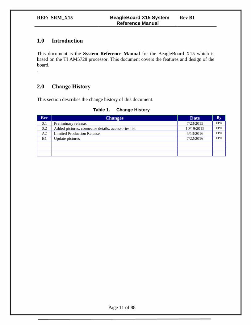
3.5.6 HIGH TEMP CAUTION
CAUTION: The BeagleBoardX15 may reach elevated temperatures.
Avoid handling the board while power is applied, especially in area shown
below. The same is true for the bottom side of the board.
Figure 41. X15 Heat Zone

REF: SRM_X15 BeagleBoard X15 System Reference Manual
Rev B1
Page 45 of 88
4.0 Hardware Design Overview
This section provides a more detailed description of the design of the board. This is
intended to provide a more complete description of each circuit. It is intended to provide
basic knowledge of the devices used and how they interface to one another. It does not
provide details of their designs or specification. Please refer to the datasheet for each
device from their respective suppliers if this information is needed.

REF: SRM_X15 BeagleBoard X15 System Reference Manual
Rev B1
Page 46 of 88
4.1 Features
The Table 2 below provides the high level features of the BeagleBoard-X15.
Table 3. BeagleBoard –X15 Features
BeagleBoard-X15
Processor Dual ARM Cortex-A15 @ 1.5GHz, TI Sitara AM5728
Graphics Dual Core SGX544 3D, 532MHZ
DSP Dual C66x, 700MHZ
Video Accelerator IVA, 532MHZ
Graphics GC3230 2D BTBLT
GP ARM Cores DUAL ARM M4, 212MHZ
SDRAM 2GB DDR3L, Dual 32bit bus, Non-ECC 533MHZ
Onboard Flash 4GB, 8bit Embedded eMMC
PMIC TPS659037
Debug Support 20-pin CTI JTAG, Serial debug header
PCB 4.2” x 4”, 12 layers
Indicators (2) Power, (4) Ethernet, (4) User Controllable
HS USB 3.0 Host (2) Type A 900ma (1) 1800mA (1)
USB 2.0 Host (1) 500mA via eSATA Connector
USB 2.0 Client (1) micro USB Type B
Ethernet (2) 10/100/1000 RJ4
SATA (1) eSATA Connector- Powered 500mA
LCD Ports (2) Via Expansion
PCIe (2) Channels via expansion
Camera Ports (1) Via expansion
SD (1) microSD
User Input (1) Reset Button (1) Power Button
HDMI (1) Full Size connector, 24b 1920x1080 60FPS, EDID
Audio HDMI and AIC3104 (Stereo In/Out)
Expansion (4) 60 pin dual row headers
GPIO pins 157
UARTs 7
SPI/I2C/CAN 1/1/1
PRU Pins 185
Real Time Clock 8pin RTC with optional battery backup, I2C I/F
Current Taps (4) 5V, 3.3V, VDD_MPU, VDD_DSP, VDD_CORE
Weight TBD
Power 12VDC@2A (3A additional if USB3 ports fully loaded)

REF: SRM_X15 BeagleBoard X15 System Reference Manual
Rev B1
Page 47 of 88
4.2 Block Diagram
The figure below is a block diagram of the board. There are more detailed block diagrams
in some of the sections that follow along with condensed schematics for the various
circuits.
Figure 42. System Block Diagram

REF: SRM_X15 BeagleBoard X15 System Reference Manual
Rev B1
Page 48 of 88
4.3 Power Subsystem
Figure 17 is the high level block diagram of the system power architecture of the board.
Figure 43. System Power Management Block Diagram
4.3.1 Input Power and Conditioning
The board is powered from a 12V 5A power supply using a 2.5mm x 5.5mm connector.
There are three switching regulators that are used to create the four main voltage rails
required by the system.
5V0………..Provides 5V to the PMIC, LEDS, HDMI, and the expansion headers.
PS3V3….….Provides the main 3.3V I/O rail supply, via the SW, and to the
PMIC.
VDD_3V3….Provides main I/O rail for the board and the expansion headers.
This is controlled by a power FET.
USB 5V…….The USB requires a lot of current to meet the USB3 requirements.
This switcher is dedicated to supplying the power to the USB3 ports.
There is a fuse provided to limit the current to the 5A rating of the power supply. The
fuse is replaceable.
12V to 5VDC 4A TPS54531
12VDC to 3.3V 4A TPS54531
FUSE 5A Slow Blow
12VDC to 5V 4A TPS54531
SW TPS22965
VDD_3V3 TPS65039
Power Management IC
PS_3V3
Syst
em V
olt
ages
USB_5V Power Button
5V0

REF: SRM_X15 BeagleBoard X15 System Reference Manual
Rev B1
Page 49 of 88
4.3.2 PMIC
The figure below is the high level block diagram of the TPS659039-Q1 Power
management IC used on the board.
Figure 44. TPS650374 Block Diagram
REF: SRM_X15 BeagleBoard X15 System Reference Manual
Rev B1
Page 50 of 88
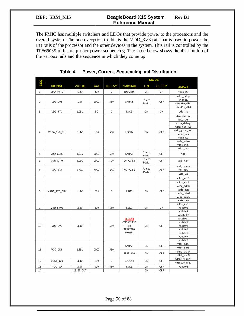
The PMIC has multiple switchers and LDOs that provide power to the processors and the
overall system. The one exception to this is the VDD_3V3 rail that is used to power the
I/O rails of the processor and the other devices in the system. This rail is controlled by the
TPS65039 to insure proper power sequencing. The table below shows the distribution of
the various rails and the sequence in which they come up.
Table 4. Power, Current, Sequencing and Distribution
SE
Q
MODE
SIGNAL VOLTS mA DELAY PMIC RAIL ON SLEEP AM57X
1 LDO_VRTC 1.8V 250 0 LDOVRTC ON ON vdda_rtc
2 VDD_1V8 1.8V 1000 550 SMPS8 Forced PWM
OFF
vdds_mlbp
vdds18v
vdds18v_ddr1
vdds18v_ddr2
3 VDD_RTC 1.05V 50 0 LDO9 ON ON vdd_rtc
4 VDDA_1V8_PLL 1.8V 100 550 LDOLN ON OFF
vdda_abe_per
vdda_ddr
vdda_debug
vdda_dsp_eve
vdda_gmac_core
vdda_gpu
vdda_iva
vdda_video
vdda_mpu
vdda_osc
5 VDD_CORE 1.03V 2000 550 SMPS6 Forced PWM
OFF vdd
6 VDD_MPU 1.09V 6000 550 SMPS1&2 Forced PWM
OFF vdd_mpu
7
1.06V
550 SMPS4&5 Forced PWM
OFF
vdd_dspeve
VDD_DSP 4000 vdd_gpu
vdd_iva
8 VDDA_1V8_PHY 1.8V 200 0 LDO3 ON OFF
vdda_usb1
vdda_usb2
vdda_hdmi
vdda_pcie
vdda_pcie0
vdda_pcie1
vdda_sata
vdda_usb3
9 VDD_SHV5 3.3V 300 550 LDO2 ON ON vddshv5
10 VDD_3V3 3.3V 550
REGEN1 (TPS54531D
via TPS22965
switch)
ON OFF
vddshv1
vddshv10
vddshv11
vddshv2
vddshv3
vddshv4
vddshv6
vddshv7
vddshv9
11 VDD_DDR 1.35V 2000 550
SMPS3 ON OFF vdds_ddr2
vdds_ddr1
TPS51200 ON OFF ddr1_vref0
ddr2_vref0
12 VUSB_3V3 3.3V 100 0 LDOUSB ON OFF vdda33v_usb1
vdda33v_usb2
13 VDD_SD 3.3V 300 550 LDO1 ON OFF vddshv8
14 RESET_OUT ON OFF

REF: SRM_X15 BeagleBoard X15 System Reference Manual
Rev B1
Page 51 of 88
In order for the board to power on, you will need to press the power button one time.
Press and release and do not hold the button down.
4.3.3 Indicators
There are two orange indicators on the board for the power rails:
DC…indicates that the 12V DC supply is connected. It does not indicate that the
voltage is within specification, but only that it is connected.
POWER…indicates that the PMIC has powered on and that the voltages are then
applied to the board. It does not indicate that any voltages are within
specification, but only that it is connected.
4.3.4 Voltage Clamp Circuits
Figure 45. Voltage Clamps
During power down it should be ensured that the difference between VDDS and
VDDSHVx [1–6] during the entire power-down sequence is < 2 V. If this is violated it
can result in reliability risks for the processor.
U35
TLVH431
Q8TRN_2N2907
VDD_3V3
VDD_1V8
R418500,1%
R429 10K,1%
R419DNI
R42040K,1%
VDD_3V3
VDD_1V8

REF: SRM_X15 BeagleBoard X15 System Reference Manual
Rev B1
Page 52 of 88
This solution was added to make sure that the difference between the 3.3-V VDDSHVx
rails and the 1.8-V VDDS rail never exceeds 2V.
4.3.5 USB Power Bus
The board is designed with a USB 3.0 HUB and supports three USB 3.0 ports. The
requirement is that each port support up to 900mA per port. For a high current charging
port, this number is raised to 1.5A. This brings the total to 3.3A max of 5V. In order to
supply this much current if needed, a dedicated 5V switcher is supplied. The figure
below shows the switcher.
Figure 46. USB 5V Switcher
The switcher is capable of supplying up to 4A. It is not expected to reach that much, but
the capacity is provided. In the event that it is required to compensate for onboard voltage
drop, the voltage level can be adjusted by changing R292 and R296 as indicated in the
datasheet for the switcher. The need for this is not expected, but a user may want to
create a little higher voltage to compensate for devices connected to the ports.
U28_6
R297
20.5
K,1
%R
294
169K
L16
4.7uH
R296
1.91K
U28_3
C410
.001uF,50V
C409
22pF
USB_SNS
U28_R
C
C401
0.1uf ,25V,0805
R295
45.3K
U28_4
12V
U28_8
12VDC TO 5VDC 4A
U28_1
U28
TPS54531D
BOOT1
VIN2
EN3
SS4
VSNS5COMP6
PH8
GND7
PA
D9
D24
SK54AFL-TP
R292
10.2K,1%C408
8.2nF,10V,0201
+ C403
100uF
,10V
USB_5V
C402
4.7
uF
,50V
.LE
SR
C440
4.7
uF
,50V
.LE
SR

REF: SRM_X15 BeagleBoard X15 System Reference Manual
Rev B1
Page 53 of 88
4.4 AM5728 Processor
This board is designed to support the AM5728 processor. For detailed information on the
AM5728 processor you can go to http://www.ti.com/product/AM5728/compare for more
information. Figure 47 is the block diagram of the AM5728 processor.
Figure 47. AM5728 Block Diagram

REF: SRM_X15 BeagleBoard X15 System Reference Manual
Rev B1
Page 54 of 88
4.5 Memory Block Diagram
Figure 48 below shows the block diagram of the memory system on the board.
Figure 48. System Memory Block Diagram
uSD ….The SD card cage that supports booting for the processor
EEPROM…provides board identification information
eMMC….provides boot source for the processor
DDR3L…main program space from which the processor operates.
Each of these are discussed in their own sections to follow.

REF: SRM_X15 BeagleBoard X15 System Reference Manual
Rev B1
Page 55 of 88
4.6 DDR3L
There are four 256Mb x16 DDR3L 2Gb (256MB) memory devices used in the design.
The memory used is either the MT41K256M16HA-125:E from Micron or the
D2516EC4BXGGB from Kingston. There are two 32 bit memory buses with two
devices on each bus.
4.6.1 DDR3 Terminations Regulator
Figure 22 below is the regulator that handles the VTT voltage rail. The regulator creates
the voltage for the termination circuits and the DDR_VREF level as well.
Figure 49. DDR3 Termination Voltages
This regulator supplies the required functions for both of the DDR3L banks on the board.
Q5 and Q6 are added to force a drain off of the VTT voltage after powering off the
system to bleed off any residual voltage left on that pin in order to prevent damage to the
processor.
DDR_VREF_OFFn19
R290 0,1%
R291 0,1%
R28910,5%
C40010pF,NPO
U27
TPS51200_10SON
VOSNS5
PGND4
VO3
PW
RP
AD
11
VLDOIN2
REFIN1
REFOUT6
EN7
GND8
PGOOD9
VIN10
R286
100K,1%
C391
.001uf ,50V
C390.001uf ,50V
R28510K,1%
C397
10uF,6.3V
C393
10uF,6.3V
C394
10uF,6.3V
C395
10uF,6.3V
VDD_3V3
VDD_DDR
DDR_VREFSTL1
DDR_VREFSTL2
VTTVTT_PGOOD
VTT_EN
VTT_VOSNS
VTT_REFOUT
C396
10uF,6.3V
DD
R_R
EF
IN
VTT_TRAN
C38910uF,6.3V
C3990.1uf ,16V
R288
10K,1%
R287
10K,1%
C3980.1uf ,16V
Q5NTA4153N
Q6BSS138PS_3V3
C392
0.1uf ,16V
R335
10K,1%
VTT
DDR_VREFSTL2 20,22
DDR_VREFSTL1 19,21
REF: SRM_X15 BeagleBoard X15 System Reference Manual
Rev B1
Page 56 of 88
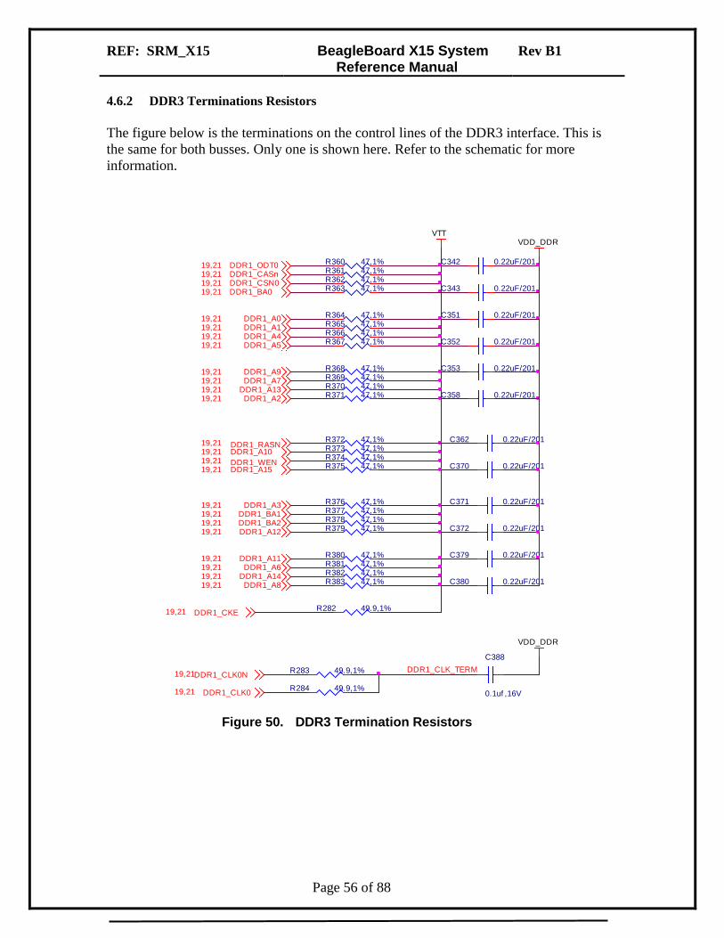
4.6.2 DDR3 Terminations Resistors
The figure below is the terminations on the control lines of the DDR3 interface. This is
the same for both busses. Only one is shown here. Refer to the schematic for more
information.
Figure 50. DDR3 Termination Resistors
DDR1_CKE19,21
DDR1_CLK0N19,21
DDR1_CLK019,21
VDD_DDR
VDD_DDR
VTT
DDR1_A519,21
DDR1_A319,21
DDR1_A119,21DDR1_A019,21
DDR1_A1119,21
DDR1_A919,21DDR1_A719,21
DDR1_A1319,21
DDR1_A1419,21
DDR1_A419,21
DDR1_A219,21
DDR1_A1519,21
DDR1_A1019,21
DDR1_A819,21
DDR1_A619,21
DDR1_BA219,21DDR1_BA119,21
DDR1_BA019,21
DDR1_A1219,21
C342 0.22uF/201
C351 0.22uF/201
C353 0.22uF/201
C343 0.22uF/201
C352 0.22uF/201
C358 0.22uF/201
C362 0.22uF/201
C370 0.22uF/201
C371 0.22uF/201
C372 0.22uF/201
C379 0.22uF/201
C380 0.22uF/201
DDR1_CSN019,21DDR1_CASn19,21DDR1_ODT019,21
R361 47,1%R360 47,1%
R363 47,1%
R282 49.9,1%
R362 47,1%
R365 47,1%R364 47,1%
R366 47,1%R367 47,1%
R283 49.9,1%
R284 49.9,1%
R368 47,1%R369 47,1%
R371 47,1%R370 47,1%
R373 47,1%R372 47,1%
R375 47,1%R374 47,1%
DDR1_WEN19,21
DDR1_RASN19,21
R376 47,1%R377 47,1%R378 47,1%R379 47,1%
R381 47,1%R380 47,1%
R383 47,1%R382 47,1%
DDR1_CLK_TERM
C388
0.1uf ,16V

REF: SRM_X15 BeagleBoard X15 System Reference Manual
Rev B1
Page 57 of 88
4.6.3 Processor Interface
The figure below shows the connections to the processor. This is the same for both
busses. Only one is shown here. Refer to the schematic for more information.
Figure 51. DDR3 Processor Interface
DDR_VREF_OFFn 24
R2741K,5%
R2731K,5%
DDR1_DQS_ECCDDR1_DQSN_ECC
VDD_DDR
U11-5
AM572x
DDR1_A14AE17
DDR1_A3AB19
DDR1_A13AF18
DDR1_RASNAF20
DDR1_BA2AB18
DDR1_A1AC19
DDR1_BA1AE18DDR1_BA0AF17
DDR1_A2AC20
DDR1_A12AC21
DDR1_A15AD18
DDR1_A10AD21
DDR1_A0AD20
DDR1_A7AE21
DDR1_A5AH22
DDR1_CASNAC18
DDR1_A11AD22
DDR1_A8AF22
DDR1_A9AE22
DDR1_A6AG23
DDR1_NCKAH24
DDR1_WENAH21
DDR1_RSTAG21
DDR1_D0AF25
DDR1_D1AF26
DDR1_D14AC24
DDR1_D11AF28
DDR1_D8AC23
DDR1_D10AG27 DDR1_D9AF27
DDR1_D15AD25
DDR1_D30AA25
DDR1_D21Y19
DDR1_D23Y20
DDR1_D29AA26
DDR1_D3AH26
DDR1_D26Y23
DDR1_D31AA28
DDR1_D27AA24
DDR1_ECC_D4Y25
DDR1_DQM2AC26
DDR1_DQS2AD27
DDR1_D24AA23
DDR1_DQSN2AD28
DDR1_D25Y22
DDR1_DQM3AA27
DDR1_D2AG26
DDR1_D22AB27
DDR1_D18AB28
DDR1_D4AF24
DDR1_D5AE24
DDR1_D6AF23
DDR1_D7AE23
DDR1_D13AC25 DDR1_D12AE26
DDR1_ECC_D7Y26
DDR1_DQM1AB23
DDR1_DQM0AD23
DDR1_D28Y24
DDR1_DQS_ECCV27
DDR1_DQS1AE27
DDR1_DQSN0AG25
DDR1_DQS3Y28
DDR1_D20AC27
DDR1_DQSN_ECCV28
DDR1_DQSN1AE28
DDR1_DQS0AH25
DDR1_DQSN3Y27
DDR1_D19AC28
DDR1_ECC_D1V23
DDR1_ECC_D5V24
DDR1_ECC_D6V25
DDR1_DQM_ECCV26
DDR1_D16V20
DDR1_D17W20
DDR1_ECC_D0W22
DDR1_ECC_D3W23
DDR1_CKAG24
DDR1_CKEAG22
DDR1_A4AF21
DDR1_CS0NAH23
DDR1_VREF0Y18
DDR1_ODT0AE20
DDR1_ECC_D2W19
GPIO7_11A22
DDR1_D021
DDR1_D321DDR1_D221DDR1_D121
DDR1_D521DDR1_D421
DDR1_D821
DDR1_D721DDR1_D621
C273
0.1uF/201
DDR1_D1121DDR1_D1021DDR1_D921
DDR1_D1321DDR1_D1221
DDR1_D1621
DDR1_D1521DDR1_D1421
DDR1_D1921DDR1_D1821DDR1_D1721
DDR1_D2121DDR1_D2021
DDR1_D2421
DDR1_D2321DDR1_D2221
DDR1_D2721DDR1_D2621DDR1_D2521
DDR1_D2921DDR1_D2821
DDR1_D3121DDR1_D3021
DDR1_DQM121
DDR1_DQM221
DDR1_DQM321
DDR1_DQM021
R3334.7K
DDR1_CKE
DDR_VREFSTL1
DDR1_WEN 21,24
DDR1_ODT0 21,24
DDR1_BA0 21,24
DDR1_RST 21
DDR1_A14 21,24
DDR1_BA2 21,24DDR1_BA1 21,24
DDR1_A2 21,24
DDR1_A13 21,24DDR1_A12 21,24
DDR1_A8 21,24
DDR1_A6 21,24
DDR1_A1 21,24
DDR1_A10 21,24
DDR1_A0 21,24
DDR1_A9 21,24
DDR1_A7 21,24
DDR1_A5 21,24
DDR1_A11 21,24
DDR1_A4 21,24
DDR1_A3 21,24
DDR1_CLK0N 21,24DDR1_CLK0 21,24
DDR1_CSN0 21,24
DDR1_A15 21,24
DDR1_CKE 21,24
DDR1_DQS021
DDR1_RASN 21,24
DDR1_CASN 21,24
DDR1_DQSN021
DDR1_DQS221
DDR1_DQS121
DDR1_DQSN221
DDR1_DQSN121
DDR1_DQSN321DDR1_DQS321
DDR_VREFSTL1

REF: SRM_X15 BeagleBoard X15 System Reference Manual
Rev B1
Page 58 of 88
4.6.4 DDR3L Connections
The figure below shows the connections to the DDR3 memory device. One device has
connections to DDRD0 to D15. The other device has connections to DDRD16 to D31 as
shown below. You will notice that the DDR data pins are scrambled. This is done to
facilitate the layout of the board and provide for an optimal layout. Address line
DDR1_A15 is not used in the default configuration as shipped. If desired a 1G DDR3
part can be used, which will double the memory on the board.
Figure 52. DDR3L Memory Device connections
R275 240,1%
DDR1_RST
DDR1_A12DDR1_A13
DDR1_BA2
DDR1_BA0DDR1_BA1
DDR1_A6
DDR1_A2DDR1_A1
DDR1_A8
DDR1_A14
DDR1_A9
DDR1_A5
DDR1_A10
DDR1_A0
DDR1_A7
DDR1_A11
DDR1_A4DDR1_A3
C276
0.22uF/201C278
0.22uF/201
DDR1_D18 19
DDR1_D23 19
DDR1_D22 19
DDR1_D17 19
DDR1_D19 19
DDR1_D21 19
DDR1_D20 19
DDR1_D28 19
DDR1_D25 19
DDR1_D16 19
DDR1_D24 19
DDR1_D29 19
DDR1_D26 19
DDR1_D27 19
DDR1_D31 19
DDR1_D30 19
DDR1_RASNDDR1_CASN
DDR1_CSN0
DDR1_WEN
DDR1_ODT0
VDD_DDRVDD_DDR
DDR_VREFSTL1
DDR1_DQM3 19
DDR1_DQM2 19
DDR1_DQS2 19
DDR1_DQS3 19DDR1_DQSN3 19
DDR1_DQSN2 19
ZQ1_HI
DDR1_CKE
DDR1_CLK0NDDR1_CLK0
DDR1_A15
U24
256MBx16 DDR3L
A12N7
A11R7
A10L7
A9R3
A8T8
A7R2
A6R8
A5P2
A4P8
A3N2
A2P3
A1P7
A0N3
BA2M3
BA1N8
BA0M2
A13T3 A14T7
ODTK1
CS#L2
CAS#K3 RAS#J3
WE#L3
CKEK9
CKJ7
CK#K7
UDQS#B7UDQSC7
LDQS#G3LDQSF3
UDMD3
LDME7
VDD.1B2
VDD.2D9
VDD.3G7
VDD.4K8
VDD.5N1
VDDQ.1A1
VDDQ.2A8
VDDQ.3C1
VDDQ.4C9
VDDQ.5D2
VDDQ.6E9
VDDQ.7F1
VDDQ.8H2
VDDQ.9H9
VDDLK2
VREFCAM8
DQ15A3
DQ14B8
DQ13A2
DQ12A7
DQ11C2
DQ10C8
DQ9C3
DQ8D7
DQ7H7
DQ6G2
DQ5H8
DQ4H3
DQ3F8
DQ2F2
DQ1F7
DQ0E3
VSS.1A9
VSS.2B3
VSS.3E1
VSS.4G8
VSS.5J8
VSSQ.1B1
VSSQ.2B9
VSSQ.3D1
VSSQ.4D8
VSSQ.5E2
VSSQ.6E8
VSSQ.7F9
VSSQ.8G1
VSSQ.9G9
VSSDLJ2
VREFDQH1
ZQL8
RSTnT2
VDD.6N9
VDD.7R1
VDD.8R9
VSS.6M1
VSS.7M9
VSS.8P1
VSS.9P9
VSS.10T1
VSS.11T9
NC.M7/A15M7
NC.L9L9
NC.L1L1
NC.J9J9
NC.J1J1

REF: SRM_X15 BeagleBoard X15 System Reference Manual
Rev B1
Page 59 of 88
4.7 4G eMMC
A single 4GB embedded MMC (eMMC) device is on the board. The device connects to
the MMC1 port of the processor, allowing for 8bit wide access. This is the secondary
boot device but as long as a bootable uSD is not inserted, it will be the primary boot
source. The expectation is that this will be the primary boot source for the board.
Figure 21 below is the connection schematic of the eMMC to the processor.
Figure 53. eMMC Circuitry
4.8 EEPROM
The board has an EEPROM for the storing of information about the board. This
information can be used by the software to determine the board’s information such as
name and revision. When J2 is installed the EEPROM can be written to. J2 is not
installed to prevent writing over the EEPROM information.
Figure 54. EEPROM Circuitry
R259
DN
I,0402
R258
DN
I,0402
RSTOUTn3,8,16,26,27
R256
DN
I,0402
R257
DN
I,0402
R255
DN
I,0402
R254
DN
I,0402
R253
DN
I,0402
R251
DN
I,0402
R250
DN
I,0402
R252
DN
I,0402
R249
0,1%
MMC2_CMD
MMC2_DAT4
MMC2_DAT1
C266
0.22uF/201
C269
0.22uF/201
U11-13
AM572x
MMC2_DAT0J4
MMC2_DAT1J6
MMC2_DAT2H4
MMC2_DAT3H5
MMC2_DAT4K7
MMC2_DAT5M7
MMC2_DAT6J5
MMC2_DAT7K6
MMC2_CLKJ7
MMC2_CMDH6
U22
MEM_MNAND_4GB
DAT0A3
DAT1A4
DAT2A5
DAT3B2
DAT4B3
DAT5B4
DAT6B5
DAT7B6
VC
CI
C2
VS
SQ
4C
4
VC
CQ
4C
6
VC
C3
E6
VS
S2
E7
VS
S5
N5
VC
C2
F5
VS
S1
G5
VS
S3
H10
VS
S4
K8
VC
C1
K9
VC
CQ
5M
4
CMDM5 CLKM6
VS
SQ
1N
2
VC
CQ
3N
4
VC
CQ
1P
3
VS
SQ
3P
4
VC
CQ
2P
5
VS
SQ
2P
6
RSTK5
VC
C0
J10
MMC2_3V3
VDD_3V3
MMC2_3V3
C268
4.7uF,6.3V
C267
2.2uF,6.3V
MMC2_CLK
EMMC_VDD1.1
VDD_3V3
MMC2_DAT3MMC2_DAT2
MMC2_DAT0
MMC2_DAT7MMC2_DAT6MMC2_DAT5
C270
0.1uf ,16V
WRITE ENABLE
U8
MEM_24WC256_8SOIC
A01
VCC8
VSS4NC3
SCL6
SDA5
A12
WP7
R3710K,1%
C810.1uf ,16V
I2C1_SDA2,3,15,16I2C1_SCL2,3,15,16
VDD_3V3
EE
WP
VDD_3V3
J2
HDR_1x1_M_.1
1 2
REF: SRM_X15 BeagleBoard X15 System Reference Manual
Rev B1
Page 60 of 88
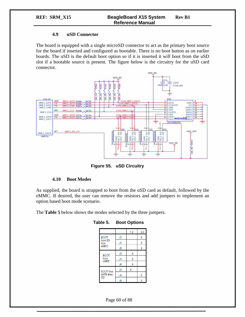
4.9 uSD Connector
The board is equipped with a single microSD connector to act as the primary boot source
for the board if inserted and configured as bootable. There is no boot button as on earlier
boards. The uSD is the default boot option so if it is inserted it will boot from the uSD
slot if a bootable source is present. The figure below is the circuitry for the uSD card
connector.
Figure 55. uSD Circuitry
4.10 Boot Modes
As supplied, the board is strapped to boot from the uSD card as default, followed by the
eMMC. If desired, the user can remove the resistors and add jumpers to implement an
option based boot mode scenario.
The Table 5 below shows the modes selected by the three jumpers.
Table 5. Boot Options
D21
TP
D2
E001
DR
L
IO1
3
IO2
5V
CC
1
GN
D4
NC
.22
D22
TP
D2E
001
DR
L
IO1
3
IO2
5V
CC
1
GN
D4
NC
.22
C271
10uF,6.3V
D23
TP
D2E
001
DR
L
IO1
3
IO2
5V
CC
1
GN
D4
NC
.22
VDD_SD
VDD_SD
VDD_SD
CON_MMC1_DAT0
VDD_3V3
MMC1_DAT2
MMC1_DAT0
MMC1_CMD
MMC1_CLK
MMC1_DAT3
MMC1_DAT1 microSD
P12
SCHA5B0200
DAT21
CD/DAT32
CMD3
VDD4
CLOCK5
VSS6
DAT07
DAT18
GND9
CD10
GND311
GND412
GND513
GND614
GND715
GND816
CON_MMC1_CLK
CON_MMC1_DAT1
MMC1_SD_CD
CON_MMC1_DAT3CON_MMC1_CMD
CON_MMC1_DAT2R266 33,5%R268 33,5%R267 33,5%
R269 33,5%
R271 33,5%R270 33,5%
R2
72
10K
,1%
U11-13
AM572x
MMC1_CLKW6
MMC1_SDCDW7
MMC1_CMDY6MMC1_DAT3Y3MMC1_DAT2AA5
MMC1_DAT0AA6
MMC1_DAT1Y4
R2
64
10K
,1%
R2
65
10K
,1%
R2
62
10K
,1%
R2
63
10K
,1%
R2
60
10K
,1%
R2
61
10K
,1%
C272
0.1uf ,16V
D20
TP
D2E
001
DR
L
IO1
3
IO2
5V
CC
1
GN
D4
NC
.22

REF: SRM_X15 BeagleBoard X15 System Reference Manual
Rev B1
Page 61 of 88
The figure below is the schematic of the boot option jumpers. By default, the board does
not have the headers loaded and there are resistors that short out pins 2 and 3 of each of
the jumpers.
Figure 56. Boot Pin Settings
The boot pins are also routed to the expansion headers. In the event an expansion board
was created, the boot modes could be overridden. Care should be taken if thee pins are
used for other functions, that they not be driven during power up when they are sampled
for the boot setting.

REF: SRM_X15 BeagleBoard X15 System Reference Manual
Rev B1
Page 62 of 88
4.11 I2C1 Bus
The I2C1 bus is only connected on the board and does not appear on the expansion
headers. There are four devices connected to this bus:
Board ID EEPROM
Temperature Sensor
TPS65074 PMIC
The figure below shows the connection between the processor and the devices.
Figure 57. I2C1 Bus
The table below provides the addresses of each of the devices on the bus.
Table 6. I2C1 Device Address
DEVICE ADDRESS FUNCTION TPS65039 0x58 Power Registers
TPS65039 0x59 Power resources
TPS65039 0x5A Trimming and test
TPS65039 0x5B OTP
TPS65039 0x12 DVS
EEPROM 0x50 Board information
TMP102 0x48 Temperature
AIC3104 0x18 Audio CODEC
U8
MEM_24WC256_8SOIC
A01
VCC8
VSS4NC3
SCL6
SDA5
A12
WP7U11-7
AM572x
I2C1_SCLC20
I2C1_SDAC21
U4
TMP102AIDRLT
ADD04
V+5
GND2
ALERT3
SCL1
SDA6
C15
0.1uf ,16V
VDD_3V3
I2C1_SCL2,7,15,16I2C1_SDA2,7,15,16
VDD_3V3
U5B
I2C1_SDA_SDIL2
I2C1_SCL_SCKL1
I2C2_SDA_SDOH8
I2C2_SCL_SCEM3
R17
2.2
K,1
%
R16
2.2
K,1
%
PMIC_SCEPMIC_SDO
R19 DNI,0402R18 DNI,0402
U18
TLV320AIC3104
SCL8
SDA9

REF: SRM_X15 BeagleBoard X15 System Reference Manual
Rev B1
Page 63 of 88
4.12 Ethernet
There a two 10/100/1000 Ethernet ports on the board that connect to the RGMII
interfaces of the processor. They are accessible via a stacked RJ45 connector.
Figure 58 below is the block diagram Ethernet section.
Figure 58. Ethernet System Block Diagram
The external circuitry is the same for both of the Ethernet PHY devices in the following
sections only port 0 will be described.
AM57xx Processor
Micrel PHY
RGMII0
Micrel PHY
RJ45
RJ45
RGMII1
INT
INT
10/100/1000
10/100/1000

REF: SRM_X15 BeagleBoard X15 System Reference Manual
Rev B1
Page 64 of 88
4.12.1 Ethernet 0 Processor Interface
Figure 59 below shows the connections between the Ethernet 0 PHY and the RGMII
interface of the processor.
Figure 59. Ethernet 0 Processor Interface
Resistors R72-R77 are used to set the default modes of the PHY. You can refer to the
KSZ903RNX datasheet for more information on these settings.
The PHY uses a 25MHz crystal to generate the required clocks.
A series of 22ohm resistors are used in series with the RX signals from the PHY to the
processor to prevent reflections. Zero ohm resistors are supplied in the TX path to
provide test points if needed. They could also be used to minimize reflections if required.
EMAC(0)_RXD2
EMAC(0)_RXD0
R_EMAC[0]_RXD3R_EMAC[0]_RXD2R_EMAC[0]_RXD1
E0_X
O
EMAC[0]_RXC
EMAC(0)_RXD3
EMAC(0)_RXD1
ETH0_3V3ETH0_3V3
R84 0,1%
R9
4D
NI,
040
2
R86 0,1%R85 0,1%
R88 0,1%R87 0,1%
R89 0,1%
ETH0_3V3
R96
0,1%
E0_
RS
T
R9212.1K,1%
R78 22,5%R79 22,5%
VDD_3V3
R80 22,5%R81 22,5%R82 22,5%R83 22,5%
R7
11
K,5
%R
70
1K
,5%
EMAC[0]_RXCTL
R7
31
K,5
%R
72
1K
,5%
R95
100K,1%,DNI
R_EMAC[0]_RXC
C217 18pF,50V
C218 18pF,50V
R7
71
0K
,1%
R7
61
0K
,1%
R7
51
0K
,1%
ENET0_INTn15
KSZ9031RNX48-pin QFN
U14
KSZ9031RNX
NC
113
LED215
DV
DD
H5
16
LED1 / PME_N117
DV
DD
L1
14
TXD019
TXD120
TXD221
TXD322
DV
DD
L5
18
DV
DD
L4
23
GTX_CLK24 TX_EN25
DV
DD
L6
26
RXD327
VS
S29
DV
DD
L2
30
RXD131 RXD032
RX_DV33
DV
DD
H3
34
RX_CLK35
MDC36 MDIO37
INT
_N
/ P
ME
_N
238
DV
DD
L3
39
DV
DD
H4
40
CL
K1
25
_N
DO
41
RE
SE
T_
N42
LD
O_O
43
XO
45
XI
46
NC
47
ISE
T48
AV
DD
H1
1
TXRXP_A2
TXRXM_A3
TXRXP_B5
TXRXM_B6
TXRXP_C7
TXRXM_C8
TXRXP_D10
TXRXM_D11
AV
DD
H2
12
RXD228
AV
DD
L_P
LL
44
P_G
ND
49
AV
DD
L2
4
AV
DD
L1
9
R7
41
0K
,1%
E0_ISET
R_EMAC[0]_RXD0
R9
31
0K
,1%
ENET_PORZ8,12
R3894.7K
ETH0_3V3
U1
4_
41
R3160,1%,DNI
MDIO_DATA 12
ETH_RESETn 12
MDIO_CLK 12MDIO_CLK
MDIO_DATA
E0_X
I
C21910uF,DNI
ETH_RESETn
Y5
25MHz
12
R_EMAC[0]_TXD1R_EMAC[0]_TXD2R_EMAC[0]_TXD3
R_EMAC[0]_TXCTL
EMAC[0]_TXD3
EMAC[0]_TXCEMAC[0]_TXCTL
R_EMAC[0]_TXCR_EMAC[0]_TXD0EMAC[0]_TXD0
EMAC[0]_TXD1EMAC[0]_TXD2
MDIO_DATA
R_EMAC[0]_RXCTL
MDIO_CLK
U11-3
AM572x
RGMII0_RXD0W2
RGMII0_RXD1Y2
RGMII0_TXD0U6
RGMII0_TXCTLV9
RGMII0_TXD2U7
MDIO_MCLKV1
RGMII0_RXD2V3
RGMII0_RXD3V4
MDIO_DU4
GPIO3_17U3
RGMII0_TXD3V7
RGMII0_TXD1V6
RGMII0_TXCW9
RGMII0_RXCTLV5
RGMII0_RXCU5

REF: SRM_X15 BeagleBoard X15 System Reference Manual
Rev B1
Page 65 of 88
An optional reset signal, GPIO3_17 is provided if there is a need for an asynchronous
reset of the PHY from the processor. This is not enabled by default. It also connects to
Ethernet 1 port as well.
4.12.2 Ethernet PHY Power
Figure 60 shows the power connections to the KSZ9031RNX PHY.
Figure 60. Ethernet Power Diagram
An external FET is required to generate the 1.2V required by the PHY core. The FET is
controlled by the PHY itself. The FET requires some heat sink function which is
provided by the PCB layout in the form of added copper.
All power for the PHY is derived from the VDD_3V3 rail, the main board power. Filters
are provided on all rails to minimize noise.
ETH0_3V3
C209
0.1uf ,16V
ETH0_3V3
C213
0.1uf ,16V
C21210uF,6.3V
C20810uF,6.3VFB2
150OHM800mA
1 2
C210
10uF,6.3V
FB1
150OHM800mA
1 2
FB4
150OHM800mA
1 2
Q1
FDT434P
E0_DVDDL
ETH0_LDO
FB3150OHM800mA
1 2
C205
47uF,6.3V,1206
KSZ9031RNX48-pin QFN
U14
KSZ9031RNX
NC
113
LED215
DV
DD
H5
16
LED1 / PME_N117
DV
DD
L1
14
TXD019
TXD120
TXD221
TXD322
DV
DD
L5
18
DV
DD
L4
23
GTX_CLK24 TX_EN25
DV
DD
L6
26
RXD327
VS
S29
DV
DD
L2
30
RXD131 RXD032
RX_DV33
DV
DD
H3
34
RX_CLK35
MDC36 MDIO37
INT
_N
/ P
ME
_N
238
DV
DD
L3
39
DV
DD
H4
40
CL
K1
25
_N
DO
41
RE
SE
T_
N42
LD
O_O
43
XO
45
XI
46
NC
47
ISE
T48
AV
DD
H1
1
TXRXP_A2
TXRXM_A3
TXRXP_B5
TXRXM_B6
TXRXP_C7
TXRXM_C8
TXRXP_D10
TXRXM_D11
AV
DD
H2
12
RXD228
AV
DD
L_P
LL
44
P_G
ND
49
AV
DD
L2
4
AV
DD
L1
9
ETH0_1.2V
VDD_3V3
E0_PLL
E0_AVDDL
C214
47uF,6.3V,1206
C211
0.1uf ,16V
C206
0.1uf ,16V
C207
0.1uf ,16V
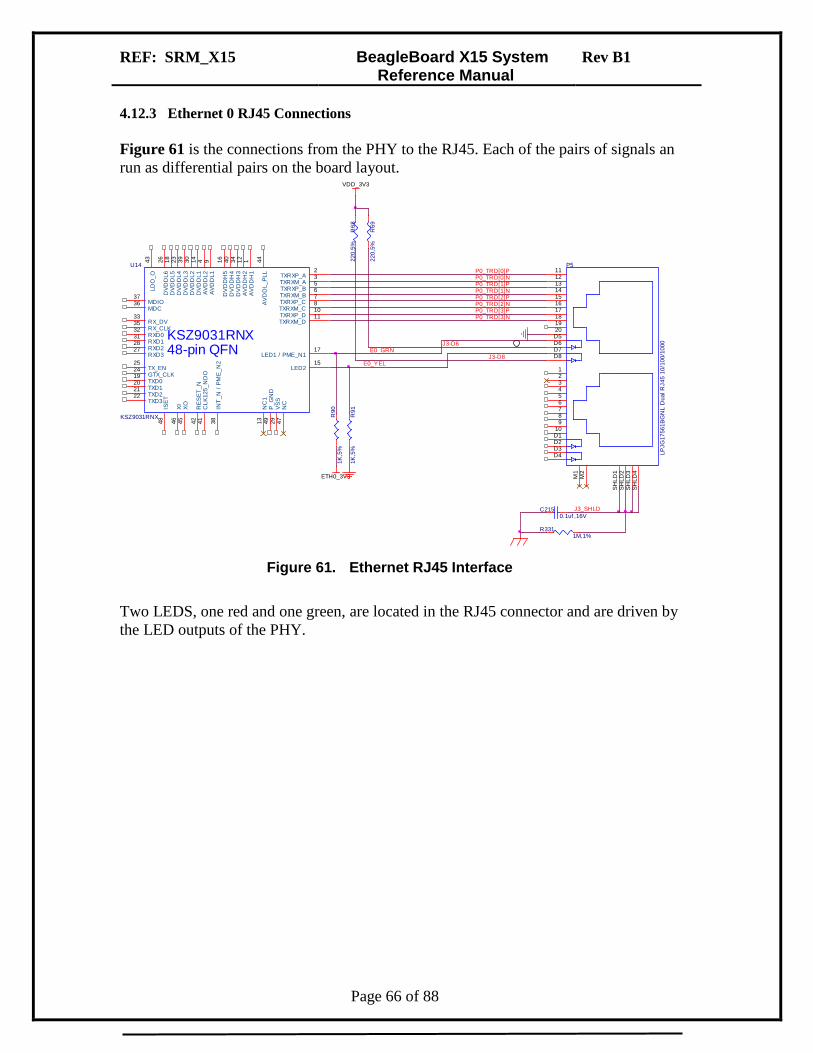
REF: SRM_X15 BeagleBoard X15 System Reference Manual
Rev B1
Page 66 of 88
4.12.3 Ethernet 0 RJ45 Connections
Figure 61 is the connections from the PHY to the RJ45. Each of the pairs of signals an
run as differential pairs on the board layout.
Figure 61. Ethernet RJ45 Interface
Two LEDS, one red and one green, are located in the RJ45 connector and are driven by
the LED outputs of the PHY.
P0_TRD[1]PP0_TRD[0]N
P0_TRD[2]NP0_TRD[2]P
P0_TRD[0]P
P0_TRD[1]N
P0_TRD[3]N
ETH0_3V3
R3311M,1%
J3-D6
P0_TRD[3]P
R6
92
20
,5%
J3-D8R
68
220
,5%
VDD_3V3
E0_YEL
E0_GRN
KSZ9031RNX48-pin QFN
U14
KSZ9031RNX
NC
113
LED215
DV
DD
H5
16
LED1 / PME_N117
DV
DD
L1
14
TXD019
TXD120
TXD221
TXD322
DV
DD
L5
18
DV
DD
L4
23
GTX_CLK24 TX_EN25
DV
DD
L6
26
RXD327
VS
S29
DV
DD
L2
30
RXD131 RXD032
RX_DV33
DV
DD
H3
34
RX_CLK35
MDC36 MDIO37
INT
_N
/ P
ME
_N
238
DV
DD
L3
39
DV
DD
H4
40
CL
K1
25
_N
DO
41
RE
SE
T_
N42
LD
O_O
43
XO
45
XI
46
NC
47
ISE
T48
AV
DD
H1
1
TXRXP_A2
TXRXM_A3
TXRXP_B5
TXRXM_B6
TXRXP_C7
TXRXM_C8
TXRXP_D10
TXRXM_D11
AV
DD
H2
12
RXD228
AV
DD
L_P
LL
44
P_G
ND
49
AV
DD
L2
4
AV
DD
L1
9
R9
01
K,5
%
R9
11
K,5
%
C2150.1uf ,16V
J3_SHLD
P5
LP
JG
17
56
1B
GN
L D
ual R
J4
5 1
0/1
00
/100
0
123456789
10D1D2D3D4
SH
LD
1S
HL
D2
M1
M2
20191817161514131211
D5D6D7D8
SH
LD
3S
HL
D4

REF: SRM_X15 BeagleBoard X15 System Reference Manual
Rev B1
Page 67 of 88
4.12.4 Ethernet 1 RJ45 Connections
Figure 37 is the connections from the PHY to the RJ45. Each of the pairs of signals are
run as differential pairs on the board layout.
Figure 62. Ethernet 1 RJ45 Interface
Two LEDS, one red and one green, are located in the RJ45 connector and are driven by
the LED outputs of the PHY.
P5
LP
JG
17561B
GN
L D
ual R
J45 1
0/1
00/1
000
123456789
10D1D2D3D4
SH
LD
1S
HLD
2
M1
M2
20191817161514131211
D5D6D7D8
SH
LD
3S
HLD
4
ETH1_3V3
R116
1K
,5%
R117
1K
,5%
KSZ9031RNX48-pin QFN
U15
KSZ9031RNX
NC
113
LED215
DV
DD
H5
16
LED1 / PME_N117
DV
DD
L1
14
TXD019
TXD120
TXD221
TXD322
DV
DD
L5
18
DV
DD
L4
23
GTX_CLK24 TX_EN25
DV
DD
L6
26
RXD327
VS
S29
DV
DD
L2
30
RXD131 RXD032
RX_DV33
DV
DD
H3
34
RX_CLK35
MDC36 MDIO37
INT
_N
/ P
ME
_N
238
DV
DD
L3
39
DV
DD
H4
40
CLK
125_N
DO
41
RE
SE
T_N
42
LD
O_O
43
XO
45
XI
46
NC
47
ISE
T48
AV
DD
H1
1
TXRXP_A2
TXRXM_A3
TXRXP_B5
TXRXM_B6
TXRXP_C7
TXRXM_C8
TXRXP_D10
TXRXM_D11
AV
DD
H2
12
RXD228
AV
DD
L_P
LL
44
P_G
ND
49
AV
DD
L2
4
AV
DD
L1
9
P1_TRD[1]N
P1_TRD[3]N
P1_TRD[1]PP1_TRD[0]N
P1_TRD[2]NP1_TRD[2]P
E1_GRN
E1_YEL
P1_TRD[3]P
P1_TRD[0]P
R98
220,5
%
J3_D2
R97
220,5
%
J3_D4
VDD_3V3

REF: SRM_X15 BeagleBoard X15 System Reference Manual
Rev B1
Page 68 of 88
4.13 HDMI
There is a single HDMI interface present on the processor. No external framer or
circuitry other than protection circuitry is required. This interface is capable of doing
1920x180 at 60 FPS.
Figure 63 below is the HDMI interface circuitry.
Figure 63. HDMI Interface Circuitry
Each of the output pairs are filtered using chokes FL1-FL4 specifically designed for
HDMI emissions suppression. This is to help on the FCC and CE emissions testing. Also
provided is ESD protection in the form of D12-D19.
U21 provides for the level shifting interface to the HDM connector. It also provides
55mA at 5V to power the EDID EEPROM on the monitor. It is not intended to provide
power for a HDMI to VGA converter.
The two pullup resistors for the I2C are not populated because the level shifter has its
own internal pullups.
A full size HDMI connector is used as the interface to the display.
VDD_3V3
C2654.7uF,6.3V
P11
HDMI-RA-19-TYPEA
D2 SHIELD2 D2+1
D2-3
D1 SHIELD5 D1+4
D1-6
D0 SHIELD8 D0+7
D0-9
CK SHIELD11 CK+10
CK-12
NC.1414 CE REMOTE13
DDC CLK15
DDC DATA16
+5V18
HP DET19
MTG1MTG1
MTG2MTG2
MTG3MTG3
MTG4MTG4
GND17
HDMI_CT_HPDHDMI_LS_OE
P11_E
SD
RHDMI_TX1-
RHDMI_TX1+
RHDMI_TX2-
RHDMI_TX2+U11-15
AM572x
HDMI1_DATA0YAH17
HDMI1_DATA1XAG18
HDMI1_DATA1YAH18
HDMI1_CLOCKXAG16
HDMI1_CLOCKYAH16
HDMI1_DATA0XAG17
HDMI1_DATA2XAG19
HDMI1_DATA2YAH19
VSSA_HDMI.2AD19
VSSA_HDMI.1AE19
HDMI_HPDB21
HDMI_CECB20
HDMI1_DDC_SDAF17HDMI1_DDC_SCLC25
GPIO7_10A24
GPIO6_28Y9
R3871M,1%
C4410.1uf ,16V
R2
46
4.7
K,D
NI
R2
45
4.7
K,D
NI
5V0
HDMI_HPD_B
HDMI_SCL_BHDMI_SDA_B
VDD_3V3
HDMI_CEC_A
D1
4
TP
D1
E0
5U
06
I1
G2
D1
2
TP
D1
E0
5U
06
I1
G2
D1
3
TP
D1
E0
5U
06
I1
G2
D1
6
TP
D1
E0
5U
06
I1
G2
D1
5
TP
D1
E0
5U
06
I1
G2
D1
7
TP
D1
E0
5U
06
I1
G2
D1
9
TP
D1
E0
5U
06
I1
G2
D1
8
TP
D1
E0
5U
06
I1
G2
HDMI_TX1-
HDMI_TX0-
HDMI_TX0+
HDMI_TXC-
HDMI_TXC+
HDMI_TX2-
HDMI_TX2+
HDMI_TX1+
HDMI_CEC_BHDMI_SDA_BHDMI_SCL_B
HDMI_HPD_B
HDMI_CEC_B
VDD_3V3
HDMI_5VOUT
HDMI_CT_HPDHDMI_LS_OE
HDMI1_DDC_SDAHDMI1_DDC_SCL
FL1
DLW21SN900HQ2
1
4 3
2
FL2
DLW21SN900HQ2
1
4 3
2
FL3
DLW21SN900HQ2
1
4 3
2
FL4
DLW21SN900HQ2
1
4 3
2
HDMI_HPD_AHDMI_CEC_A
R247 10K,1%,DNIR248 10K,1%
5V0
VDD_3V3
U21
TPD12S016 24UQFN
SCL_A1
SDA_A2
CEC_A24 HPD_A
3
CEC_B6HPD_B9
SCL_B7SDA_B8
VCCA23
LS_OE4 CT_HPD
11
5V_OUT12
VCC_5V10
D1+20
D1-19
D2+22
D2-21
D0+17
D0-16
CLK+15
CLK-14
GN
D1
5
GN
D3
18
GN
D2
13
55mA MAX
C2640.1uf ,16V
RHDMI_TX0+
RHDMI_TX0-
RHDMI_TXC-
RHDMI_TXC+
R2
42
DN
I,0
40
2
HDMI_HPD_A
R2
41
DN
I,0
40
2
R2
37
DN
I,0
40
2

REF: SRM_X15 BeagleBoard X15 System Reference Manual
Rev B1
Page 69 of 88
4.1 Audio
There are two sources of audio from the board, the HDMI interface or the stereo
CODEC. Only the CODEC will support Audio input. This section covers the stereo
CODEC.
4.1.1 Processor Interface
Figure 64 below shows the interface between the processor and the AIC3104.
Figure 64. Stereo CODEC Processor Interface
The AIC3104 requires a master clock (MCLK) that is supplied by the processor using
the XREF_CLK1 pin. Depending on the requirements, this clock can be any range from
512KHz to 50MHz. The most likely frequencies to be used are 12MHZ, 13MHZ,
16MHz, 19.2MHZ or 19.68MHZ.
Connection to the processor uses the McASP3 I2S interface.
RSTOUTn signal provides a reset to the AIC3014 whenever the system is reset.
The I2C1 interface is used to change the internal registers of the AIC3104. The I2C
address is 0x18.
R224 10,5%
R225 10,5%R227 10,5%
R229 10,5%
R223 22,5%
U18
TLV320AIC3104
RESETn31
SCL8
SDA9
MCLK1
WCLK3
BCLK2
DIN4
DOUT5
U11-17
AM572x
MCASP3_ACLKXB18MCASP3_FSXF15
MCASP3_AXR0B19
MCASP3_AXR1C17
XREF_CLK1E17
I2C1_SDA2,3,7,15I2C1_SCL2,3,7,15
RSTOUTn3,8,18,26,27
AIC_MCLKAIC_WCLKRAIC_BCLKR
AIC_MCLKR
AIC_DOUTRAIC_DINR
AIC_WCLKAIC_BCLK
AIC_DOUTAIC_DIN
R231
20K
,1%
R232
20K
,1%

REF: SRM_X15 BeagleBoard X15 System Reference Manual
Rev B1
Page 70 of 88
4.1.2 Power Circuitry
Figure 65 below is the power circuitry for the AIC3104.
Figure 65. AIC3104 Power Circuitry
The primary power source is the VDD_3V3 rail. You will notice a filter is used on the
rail in order to keep the noise down on the audio I/O. After the filter the rail becomes the
VDAC_3CV3 rail. This rail is then run through ferrite beads to create the AVDD_DAC,
IOVDD, and DRVDD rails.
The core circuitry inside the AIC3104 requires a 1.8V power rail on the DVDD pin. The
TPS77018 device generates that voltage from the VDAC_3V3 rail.
There is a separate ground plane under the CODEC that connects to the system ground at
a single point through FB9, a ferrite bead, in order to minimize any noise that might be
present in the ground plane.
AGND_AUD
AGND_AUD
U18
TLV320AIC3104
AVDD_DAC25
DRVDD18
IOVDD7
DVDD32
DVSS6
AVSS_ADC17
AVSS_DAC26
DRVSS21
DRVDD24
PAD33
VDAC_3V3
VDAC_3V3
VDAC_3V3
VDAC_3V3 U19
TPS77018DBV
IN1
GND2
ENn3
NC/FB4
OUT5
FB9
150OHM800mA
1 2
C25410uF,6.3V
C25710uF,6.3V
C24910uF,6.3V
VDD_3V3
C260
1uF,4V,0201
L13
BLM21PG221SN1D
L15
BLM21PG221SN1D
L14 BLM21PG221SN1D
C2530.1uf ,16V
C2520.1uf ,16V
C2580.1uf ,16V
C2590.1uf ,16V
C2620.1uf ,16V
C2470.1uf ,16V
L12
FLT_HIFREQ_.47UF
1 3
2 C2480.1uf ,16V
C2614.7uF,6.3V
AIC_IOVDD3.3
AIC_DRVDD3.3
AIC_DVDD
AIC_AVDD_DAC3.3

REF: SRM_X15 BeagleBoard X15 System Reference Manual
Rev B1
Page 71 of 88
4.1.3 Audio In/Out
Figure 66 is the audio jacks for the Audio in and out.
Figure 66. Stereo CODEC Audio Connections
Each of the connectors is a 3.5mm stereo jack. D8-D11 provides ESD protection for the
user connections. The termination signals on the interfaces are connected to a single point
ground. In the layout is a single dedicated ground for the CODEC circuitry. It is
connected to the system ground through FB9.
R230 10,5%
R233 10,5%
U18
TLV320AIC3104
RESETn31
SCL8
SDA9
MCLK1
WCLK3
BCLK2
DIN4
DOUT5
LEFT_LOP27
LEFT_LOM28
RIGHT_LOP29RIGHT_ROM30
HPLOUT19
HPROUT23
HPRCOM22
HPLCOM20
IN2R16
MICBIAS15
IN2L14
IN1LP10
IM1LM11
IN1RP12
IN1RM13
AVDD_DAC25
DRVDD18
IOVDD7
DVDD32
DVSS6
AVSS_ADC17
AVSS_DAC26
DRVSS21
DRVDD24
PAD33
RIGHT_IN
C255 2.2uF,6.3V
C256 2.2uF,6.3V
FB9
150OHM800mA
1 2
D8
PE
SD
0603-2
40
D9
PE
SD
0603-2
40
D10
PE
SD
0603-2
40
D11
PE
SD
0603-2
40I2C1 ADDRESS 0X18
C251 47uF,6.3V,1206
C250 47uF,6.3V,1206
R235
20K
,1%
R234
20K
,1%
R226
20K
,1%
R228
20K
,1%
AUDIO_R RIGHT_OUT
LEFT_OUT
AUDIN_L LEFT_IN
P8
SJ1-3524NG
1
2
3
4
AUDIN_RR
AUDIN_R AUDIN_RL
AUDIO_L
P9
SJ1-3524NG
1
2
3
4

REF: SRM_X15 BeagleBoard X15 System Reference Manual
Rev B1
Page 72 of 88
4.2 USB 2.0 Client Port
The board has a single USB OTG port that is configured as a Client port by default. The
Figure 67 shows the design of the circuit. D40 provides the ESD protection for the
signals.
If you look at the full schematic you will see an option for routing these signals to an
expansion board. You can swap R321 and R320, putting the port into a host mode. If you
want to use it as an OTG port, an ID pin would need to be provided to the processor via a
GPIO pin. There is no dedicate ID pin on the processor.
Figure 67. USB Client Port
There is a VBUS detection circuit on the board. You will notice that it is isolated and not
used.. This was put into the design to compensate for the function not working correctly
in the PMIC> Once the PMIC was fixed, the circuit was no longer needed. In future
revisions, this circuitry will be removed from the assembly. It is left there for now, just in
case the PMIC falls ill again. Figure 68 shows this circuitry and the isolation points.
The USB2_VBUS connects direct to the PMIC and the PMIC_VBUS_DET is the output
from the PMIC confirming the detection.
R21127,1%R21027,1%
P7_SHLD
P7
Mic
ro U
SB
-AB
D-2D+3
VB1
ID4
G2
S1
G3
S2
G15G
5S
4
G4
S3
U11-10
AM572x
USB2_DMAF11USB2_DPAE11GPIO7_24E25
US
B2_D
PU
SB
2_D
M
R3861M,1%
C2310.1uf ,16V
D40
TPD2E001DRL
IO1
3IO
25
VC
C1
GN
D4
NC
.22
USB1_VBUS
USBSP_DPUSBSP_DM
R32010K,1%,DNI
R32110K,1%USB2_ID
VDD_3V3

REF: SRM_X15 BeagleBoard X15 System Reference Manual
Rev B1
Page 73 of 88
Figure 68. Alternate VBUS Detect Circuitry
R3200,1%,DNI
USB2VBUS_EXP 27
R310,1%,DNI
U42
SN74LVC1G06DCK
A2
Y4
GN
D3
VC
C5
NC
1
VDD_3V3
R408
47K,1%
R409 620K
VBUS_DET 13
R410 330K
VDD_3V3
Q7BSS138/SOT
R413 0,1%,DNIUSB2_VBUS 3
USB2_5V
C4951uF,30V,0402
R412 0,1%
R415
47K,1%
PMIC_VBUS_DET3
VDD_3V3
R4140,1%

REF: SRM_X15 BeagleBoard X15 System Reference Manual
Rev B1
Page 74 of 88
4.3 USB 3.0 and HUB
There are three USB3 ports on the board, implemented by using a USB3 HUB connected
to the processor. The processor only has one USB3 port and requires the HUB to handle
additional ports.
4.3.1 Processor and HUB Interface
Figure 69 shows the main connections between the processor and the HUB.
Figure 69. USB3 and HUB Processor Interface
The USB signals are connected between the HUB and the processor via capacitors. The
TX and RX lines are swapped between the two.
There is not a dedicated ID pin for the ID function, so GPIO7_26 is used for that
function. Pulling it low sets the port to host mode. The I2C3 port is not connected by
default and is not currently being used for processor to HUB communications.
U11-10
AM572x
USB_RXN0AF12
USB_RXP0AE12
USB_TXN0AC11
USB_TXP0AD11
USB1_DMAC12USB1_DPAD12USB1_DRVVBUSAB10
GPIO7_25C27
I2C3_SDAC14
I2C3_SCLD14
USB1_DM
USB1_DRVVBUSUSB1_DP
USB_SSRXP0
USB_SSRXM0
PUSB_TXP0
PUSB_TXN0 C244 0.1uf ,16V
C239 0.1uf ,16V
USB_SSTXP0
USB_SSTXM0
PUSB_RXP0
PUSB_RXN0
C241 0.1uf ,16V
C242 0.1uf ,16V
R20510K,1%
USB1_ID
U17
TUSB8040A
USB_VBUSB44
USB_DP_UPA46
USB_DM_UPB42
USB_SSRXP_UPA44
USB_SSRXM_UPB40
USB_SSTXP_UPB39
USB_SSTXM_UPA42
SCL_SMBCLKB17 SDA_SMBDATA19
R3
92
2.2
K,1
%R
391
2.2
K,1
%
VDD_3V3

REF: SRM_X15 BeagleBoard X15 System Reference Manual
Rev B1
Page 75 of 88
4.3.2 USB3 Port Power Control
Figure 70 is the power control for the USB3 ports. Each rail is controlled by the USB
HUB. Each voltage rail has filter caps, bulk caps, and a ferrite bead for noise emissions
reduction. Resistors R293 and R298 set the current limit on each of the switches. Ports 1
and 2 are set for the 1200mA charge current. Only port one has that function enabled at
the HUB. The other USB3 port, port 3, is set for 900mA.
Figure 70. USB3 Power Control
The USB4VBUS is in support of the eSATA connector and can deliver 900mA to the
eSATA port.
USB3V
R293
25.5K,1%
C4
14
0.1
uf,
16V
+C4
13
100
uF
,10V
USB3VBUS
BATEN014
BATEN114
OC014
OC114
BATEN214
BATEN314
OC214
OC314
USB_5V
USB4V
U29_7
U30_7
C4
05
0.1
uf,
16V
C4
12
0.1
uf,
16V
+C4
11
100
uF
,10V
+C4
04
100uF
,10V
+C4
06
100uF
,10V
R298
63.4K,1%
L18BLM21PG221SN1D
C4
07
0.1
uf,
16V
USB2VUSB1V USB1VBUS
L17BLM21PG221SN1D
USB2VBUS
L19BLM21PG221SN1D
L20BLM21PG221SN1D
USB4VBUS
U30
TPS2561DRC
IN12
IN23
EN14
EN25
FAULT110
FAULT26
OUT19
OUT28
ILIM7
GND1
PAD11
U29
TPS2561DRC
IN12
IN23
EN14
EN25
FAULT110
FAULT26
OUT19
OUT28
ILIM7
GND1
PAD11

REF: SRM_X15 BeagleBoard X15 System Reference Manual
Rev B1
Page 76 of 88
4.3.3 USB3 Port Connectors
Figure 71 shows connections to the connectors on the board. The port has ESD
protection on all signals. P13 is a single USB 3.0 connector.
Figure 71. USB Port 1 Connectors
Figure 72 shows the connection for USB3 ports 2 and 3. P15 is a dual stacked UBS 3.0
connector. Each pin has a dedicated ESD device.
Figure 72. USB Port 2 and 3 Connectors
P13
CONN_USB3.0_A
USBVDD1
D+3 D-2
RX-5
RX+6
GNDD7TX-
8
TX+9
SHLD010
GND4SHLD111
C446 0.1uf ,16VC447 0.1uf ,16V
USB_DM014
USB_DP014
USB_TXM014
USB_TXP014
USB_RXM014
USB_RXP014
D25
TP
D2E
US
B30A
DR
D+
1
D-
2G
ND
3
D35
TP
D1E
10B
06
IO1
GN
D2
D27
TP
D2E
US
B30A
DR
D+
1
D-
2G
ND
3
D26
TP
D2E
US
B30A
DR
D+
1
D-
2G
ND
3
TX-TX+
USB1VBUS
C4
19
0.1
uf,
16V
USB2VBUS
D3
6
TP
D1
E1
0B
06
IO1
GN
D2
D3
4
TP
D1
E1
0B
06
IO1
GN
D2
C448 0.1uf ,16V
USB3VBUS
C450 0.1uf ,16V
C449 0.1uf ,16V
C451 0.1uf ,16V
D38
TPD2EUSB30ADR
D+1
D-2 GND
3
D29
TPD2EUSB30ADR
D+1
D-2 GND
3
TX2+
TX1-TX1+
TX2-
USB_RXM114
USB_RXP114
USB_DP114USB_DM114
USB_TXM114
USB_TXP114
USB_RXP214
USB_DP214USB_DM214
USB_TXM214
USB_TXP214
USB_RXM214
D28
TPD2EUSB30ADR
D+1
D-2 GND
3
D31
TPD2EUSB30ADR
D+1
D-2GND
3
D33
TP
D2
EU
SB
30A
DRD
+1
D-
2
GN
D3
D30
TP
D2
EU
SB
30A
DRD
+1
D-
2
GN
D3
P15
GSB311231HR
VBUS01
D0+3 D0-2
RX0+6 RX0-5
GNDD07
TX0+9 TX0-8
SHLD019
GND04
VBUS110
D1-11
D1+12
RX1-14
RX1+15
TX1+18 TX1-17
GND113
GNDD116
SHLD120
SHLD221
SHLD322
R3
00
1M
,1%

REF: SRM_X15 BeagleBoard X15 System Reference Manual
Rev B1
Page 77 of 88
4.4 eSATA/SATA
Figure 73 is the block diagram of the SATA section.
Figure 73. eSATA Block Diagram
A switch is used to direct the SATA signals to the onboard eSATA connector or to the
expansion header, where they can be used by add-on boards. If the signal on the
expansion header, P19-4, is left open, the signals go to the eSATA onboard connector. If
the pin is grounded, the switch is activated and the signals are routed to the expansion
headers. If the SATA signals are routed to the expansion headers, the eSATA connector
can still be used as USB port.
The Figure 74 is the detailed design of the eSATA interface. The eSATA interface is a
combination of two separate interfaces, SATA and USB. The eSATA port can be used as
an eSATA or a USB 2.0 port. Power for the eSATA is from the USB power pins, 5V.
The USB signals originate from the USB 3.0 HUB. The SATA interfaces originate from
the AM5728 processor via the switch.
Power is routed to the eSATA connector via the TPS2560 FET switch. It is capable of
providing the 5V at 900mA required by the eSATA connector.
AM57xx Processor
SATA
SWITCH
eSATA
EXPANS ION SATA_SEL

REF: SRM_X15 BeagleBoard X15 System Reference Manual
Rev B1
Page 78 of 88
Figure 74. eSATA Circuitry
SATA_RXN0
SATA_TXP0
SATA_RXP0
SATA_TXN0
EXP_SATA_RXN27
EXP_SATA_TXN27EXP_SATA_TXP27
EXP_SATA_RXP27
VDDA_1V8_PHY
C421
0.1uF/201
L21
FLT_HIFREQ_.47UF
1 3
2
VDD_1V8
R301 0,1%,DNI
R302 0,1%
R303
1K,5%
U31_VDDU31_1V8
U31
PI2DBS212_TQFN
GN
D1
1
SEL3
A0+4
A0-5
A1+6
A1-7
VD
D1
9G
ND
210
C1-15 C1+16 C0-17 C0+18
VD
D3
13
GN
D6
25
B1-21 B1+22 B0-23 B0+24
NC2 NC18
VD
D2
11
GN
D3
12
GN
D4
14
VD
D4
19
GN
D5
20
VD
D5
26
VD
D6
28
GN
D7
27
U11-1
AM572x
SATA1_RXN0AH9
SATA1_RXP0AG9
SATA1_TXN0AG10
SATA1_TXP0AH10
VSSA_SATAAE10
C415
0.1uf ,16V
C416 0.1uf ,16V
USB4VBUS
C420 0.1uf ,16V
C418 0.1uf ,16V
C417 0.1uf ,16V
eSATA_T+
eSATA_R-
eSATA_T-
eSATA_R+
US
BS
AT
A
P6
eSATA
VBUS01
D-2
D+3
GND14
GND25
A+6
A-7
GND38
B-9
B+10
GND411
M112M213
S114S215S316S417 P20_SHLD
R2991M,1%
TO THEEXPANSIONHEADER.
TUSB8040A
U17
USB_DP_DN3B29USB_DM_DN3A31
PWRON3Z_BATEN3A22
OVERCUR3ZA24
USB_5V
U30_7
R298
25.5K,1%
U30
TPS2560DRC
IN12
IN23
EN14
EN25
FAULT110
FAULT26
OUT19
OUT28
ILIM7
GND1
PAD11
C414
0.1
uf,
16V
+C413
100uF
,10V

REF: SRM_X15 BeagleBoard X15 System Reference Manual
Rev B1
Page 79 of 88
4.5 Serial Debug Port
The Figure 75 is the serial debug port on the board. It provides TX, RX, and ground
signals. The SN74LVC2G241 is an isolation buffer to prevent the signals from being fed
back into the processor when the board is powered off.
Figure 75. Debug Serial Port
The TX and RX signals are 3.3V level. In order to connect them to a PC, a USB to serial
converter is required. A common one is the FTDI USB to TTL cable as shown in Figure
76 below. May sure you use the 3.3V version and not the 5V version.
Figure 76. FTDI USB to Serial Adapter
UART3_TXD15UART3_RXD15
R236
10K
,1%
B_UART0_TXB_UART0_RX
U20
SN74LVC2G241
1A2
2OE7 1OE
1VCC
8
GND4
2A5 2Y
31Y
6
C2630.1uf ,16V P10
HEADER 6
123456
VDD_3V3
VDD_3V3
Serial Debug
Cable
Pin 1

REF: SRM_X15 BeagleBoard X15 System Reference Manual
Rev B1
Page 80 of 88
4.6 JTAG Connector
A JTAG connector is provided for those requiring advanced debug capability. Because
the AM5728 processor has a pair of DSPs, those using the DSP may find this feature very
useful. Figure 77 below shoes the connection diagram.
Figure 77. JTAG Port
4.7 Temperature Sensor
A TMP102A temperture sensor is located nearthe processor. There is also a temperature
sensor inside the processor. This sensor is intended to measure the ambient temperature
near the processor. The sensor is connected to the I2C3 bus on the processor. The alert
pin that indicates the the temperature has exceeded th eset limit is onnected to GPIO7_16.
Figure 78 below shows the temperature sensor circuitry.
Figure 78. Temperature Sensor Circuitry
R61 22,5%R63 22,5%
R65 22,5%
R60 22,5%
R64 22,5%
U11-14
AM572x
EMU1D24
TDID23
EMU0G21
RTCKE18
TCLKE20
TDOF19
TRSTND20
TMSF18
R67 22,5%
R5
94
.7K
R624.7K
R664.7K
EMU_RSTn
P4
20 Pin JTAG
SRST15
GND.18
GND.210
GND.312
GND.416
GND.520
EMU013
EMU114
EMU217
EMU318
TCLK11
EMU419
KEY6TDIS4
TDO7
TDI3 TRSTn
2TMS
1
TVD5
TCKRTN9
VDD_3V3
VDD_3V3
VDD_3V3
EMU1
RTCKTCK
EMU0
TDO
TMS
RTCKR
EMUR
TDITDIR
TDOR
TCLK
TRSTN
EMU_RSTn
EMU1R
C15
0.1uf ,16VU4
TMP102AIDRLT
ADD04
V+5
GND2
ALERT3
SCL1
SDA6I2C1_SCL3,7,15,16
I2C1_SDA3,7,15,16
VDD_3V3
TMP102_ALERT 15
VDD_3V3
R154.7K

REF: SRM_X15 BeagleBoard X15 System Reference Manual
Rev B1
Page 81 of 88
4.8 Real Time Clock
A battery back external Real Time Clock (RTC) MCP79410 is provided to keep the
current clock active while the board is powered down. It can be used in conjunction with
the internal Real Time Clock of the processor which will reset when power is removed
from the board.
In addition to the typical RTC functions, the device has 64 bytes of battery backed RAM
and 1Kb of EEPROM.
The CR1229 non-rechargeable battery supplies 35mAh of backup power which is
sufficient to keep the RTC active for a couple of years. Make sure you do not short the
battery by placing the board on a conductive surface when not in use as you will lose the
time.
Figure 79 below is the RTC circuitry.
Figure 79. Real Time Clock Circuitry
The RTC_ALARM connects to the Wakeup3 signal on the processor.
Communication to the processor uses the I2C3 bus. Registers and settings can be found
in the RTC datasheet.
VDD_3V3
R391
2.2
K,1
%R
392
2.2
K,1
%
U11-7
AM572x
I2C3_SDAC14
I2CS_SCLD14
R33
4.7
5K
,1%
VDD_3V3
C30 0.1uf ,16V
BAT1
CR-1220/FCN
+1
-2
U6
MCP79410,TFDN
X11
X22
VBAT3
VSS4
VCC8
MFP7
SCL6
SDA5
RTC_X2RTC_X1
RTC_ALARM
Y1CFS206-32.768KDZB
1 2
C3110pF,50V
C3210pF,50V
BU_BATT
VDD_3V3

REF: SRM_X15 BeagleBoard X15 System Reference Manual
Rev B1
Page 82 of 88
4.9 User LEDs
There are four User LEDS on the board. By setting the corresponding GPIO pin to a 1,
the LED will turn on. Figure 80 shows the User LED circuitry.
Figure 80. User LEDs Circuitry
Table 7 below gives the GPIO pins used for each LED.
Table 7. User LED GPIO Mapping
LED GPIO PIN USER0 GPIO7_8
USER1 GPIO7_9
USER2 GPIO7_14
USER3 GPIO7_15
USR0 USR1
USR0 LE
DB
C
LE
DA
C
LE
DB
A
5V0
LE
DA
A
USR2
USR1 LE
DD
C
LE
DC
C
USR3
USR3USR2
LE
DC
A
LE
DD
A
R2154.7K
R2164.7K
R2174.7K
R2184.7K
U11-12
AM572x
GPIO7_15B22
GPIO7_9B25GPIO7_8F16
GPIO7_14A26
R222
100K,1%
R221
100K,1%
R220
100K,1%
R219
100K,1%
D4
LTST-C191KFKT D5
LTST-C191KFKT
D6
LTST-C191KFKT
D7
LTST-C191KFKT
47k
10k
Q3A
DMC56404
16
2
47k
10k
Q3B
DMC56404
43
5
47k
10k
Q4A
DMC56404
16
2
47k
10k
Q4B
DMC56404
43
5
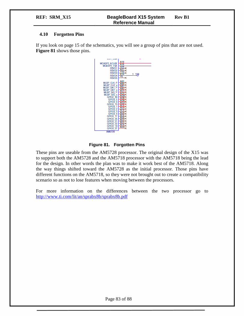
REF: SRM_X15 BeagleBoard X15 System Reference Manual
Rev B1
Page 83 of 88
4.10 Forgotten Pins
If you look on page 15 of the schematics, you will see a group of pins that are not used.
Figure 81 shows those pins.
Figure 81. Forgotten Pins
These pins are useable from the AM5728 processor. The original design of the X15 was
to support both the AM5728 and the AM5718 processor with the AM5718 being the lead
for the design. In other words the plan was to make it work best of the AM5718. Along
the way things shifted toward the AM5728 as the initial processor. Those pins have
different functions on the AM5718, so they were not brought out to create a compatibility
scenario so as not to lose features when moving between the processors.
For more information on the differences between the two processor go to
http://www.ti.com/lit/an/sprabx8b/sprabx8b.pdf

REF: SRM_X15 BeagleBoard X15 System Reference Manual
Rev B1
Page 84 of 88
5.0 Expansion Connectors
There are four expansion connectors on the board. The connector used are the Hirose
FX18 series. Figure 82 below is a picture of the connector.
Figure 82. Expansion Connector
When the alpha board was designed, .025 pins and headers were used. The insertion force
and retention force of those connectors made them impossible to use as there were too
may signals. It was impossible to get the boards pulled apart.
On the final version the Hirose connector was used to reduce the insertion and removal
force significantly and to provide for higher speed signal handing required by the PCIe
and SATA signals.
5.1 Expansion Header Pinouts
The following pages cover the functions found on the expansion headers. The actual
pinout is not covered in this document. This information can be found in the Pin Map
spreadsheet that is sortable on all columns, making it easier to search for pins across
various categories such as:
By expansion header
By function (PRU, LCD, etc.)
By name
The Pin Map spreadsheet can be found on the X15 Support Wiki.

REF: SRM_X15 BeagleBoard X15 System Reference Manual
Rev B1
Page 85 of 88
http://elinux.org/BeagleBoard:BeagleBoard-X15
5.1 Creating and Expansion Board
The expansion connectors are located on the bottom side of the board. There are three
possible options for creating your own expansion board.
Create a board that connects to one expansion connector
Create a board that connects to two of the connectors
Create a board that connects to all 4 connectors
Figure 83 below shows the dimensions of the board and the placement of the connectors.
This view is looking through the X15. This would also be the same view used for any
expansion board that were designed. The expansion board mounts on the back side of the
board. DO NOT mount the X15 under the expansion board, unless it is mounted at an
angle to where you get proper airflow, such as when used with an LCD panel.
Figure 83. Expansion Board Measurements

REF: SRM_X15 BeagleBoard X15 System Reference Manual
Rev B1
Page 86 of 88
The mating connector is the Hirose FX18-60S-0.8SV15. If you need different heights
than this one, they are available as well. Figure 84 is a picture of this connector.
Figure 84. Expansion Mating Expansion Connector
These connectors can be purchased from the following suppliers:
http://www.digikey.com/product-search/en?keywords=FX18-60S-0.8SV15
http://www.mouser.com/ProductDetail/Hirose-Connector/FX18-60S-
08SV15/?qs=sGAEpiMZZMvffgRu4KC1R93sqY37AFrhtQh7fBPpuqI%3d
http://www.newark.com/hirose-hrs/fx18-60s-0-8sv15/connector-rcpt-60pos-2row-0-
8mm/dp/59Y7142?ost=FX18-60S-0.8SV15&categoryId=&categoryName=
http://www.sager.com/fx18-60s-0-8sv15-3614937.html
https://estore.heilind.com/FX18-60S-0.8SV15/HIRFX18-60S-0.8SV15.html
Supply will vary so leave yourself enough time when ordering the parts.

REF: SRM_X15 BeagleBoard X15 System Reference Manual
Rev B1
Page 87 of 88
Figure 85. X15 Top Side View

REF: SRM_X15 BeagleBoard X15 System Reference Manual
Rev B1
Page 88 of 88
Figure 86. X15 Bottom Side View

Mouser Electronics
Authorized Distributor
Click to View Pricing, Inventory, Delivery & Lifecycle Information: BeagleBoard:
BeagleBoard X15