Embed Size (px)
Citation preview
Sie
na 2
013
Sili
con
Aval
anch
e Pi
xel (
APi
X)
Silicon Avalanche Pixel Structures (APiX) For Coordinate Measurements
V.Saveliev Institute of Applied Mathematics, Russian Academy of Science
on behalf of APiX Project
M.G. Bagliesi(a), G. Bigongiari(a), S. Bonechi(a), P. Brogi(a), G. Collazuol(d), N.D’Ascenzo(g), P. Maestro(a), P.S. Marrocchesi(a), C.S. Moon(f,b), F. Morsani(b), L. Ratti(c), V.Saveliev(g),
A. Savoy Navarro(f,b), J.E. Suh(a), A. Sulaj (a), C. Vacchi(c), S. Zucca(e)
Univ. of Siena and INFN Gruppo Collegato (Italy) INFN Sezione di Pisa (Italy)
Univ. of Pavia and INFN Sezione di Pavia (Italy) Univ. of Padova (Italy)
Laboratoire APC, Université Paris-Diderot/CNRS (France) Institute of Applied Mathematics, Russian Academy of Science, Moscow (Russia)
Sie
na 2
013
Sili
con
Aval
anch
e Pi
xel (
APi
X)
2
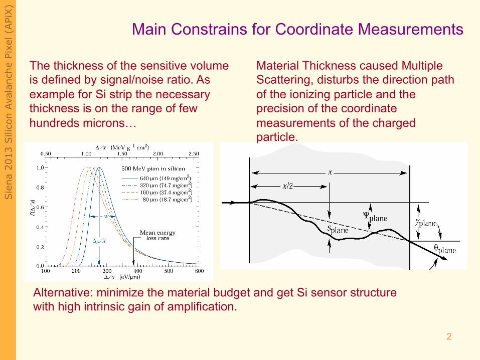
Main Constrains for Coordinate Measurements
The thickness of the sensitive volume is defined by signal/noise ratio. As example for Si strip the necessary thickness is on the range of few hundreds microns…
Alternative: minimize the material budget and get Si sensor structure with high intrinsic gain of amplification.
Material Thickness caused Multiple Scattering, disturbs the direction path of the ionizing particle and the precision of the coordinate measurements of the charged particle.
Sie
na 2
013
Sili
con
Aval
anch
e Pi
xel (
APi
X)
3
l The detection of ionizing particles imposes a certain material budget due to the necessity of sensitive material, - the signal is proportional to the path length in sensitive material (ionization energy loses);
l The coordinate measurements of ionizing particles are affected by the material budget, - Multiple Scattering is disturbing the direction of particles and thus the precision in tracking);
l The signal quality is affected by the electronic noise - including the detector itself; the signal without an internal amplification is not so strong;
l The need for the front end electronics very close to the sensors is increasing the material budget dramatically (second wafer for electronics);
Coordinate Measurement of Ionizing Particles
(conventional)
Sie
na 2
013
Sili
con
Aval
anch
e Pi
xel (
APi
X)
4
YES :
l The minimal sensitive thickness (few microns) gives very strong signal for ionizing particle;
BUT :
l Silicon Photomultiplier has quite high dark rate (~10 5/mm2), could not be distinguishing from signal of ionizing particle;
l High Sensitivity to background photons;
l Don’t have the pixel by pixel (cell by sell) readout, coordinate measurements have to have the single pixel (cell) readout;
Can Silicon Photomultiplier Detect the Ionizing Particles ?
Sie
na 2
013
Sili
con
Aval
anch
e Pi
xel (
APi
X)
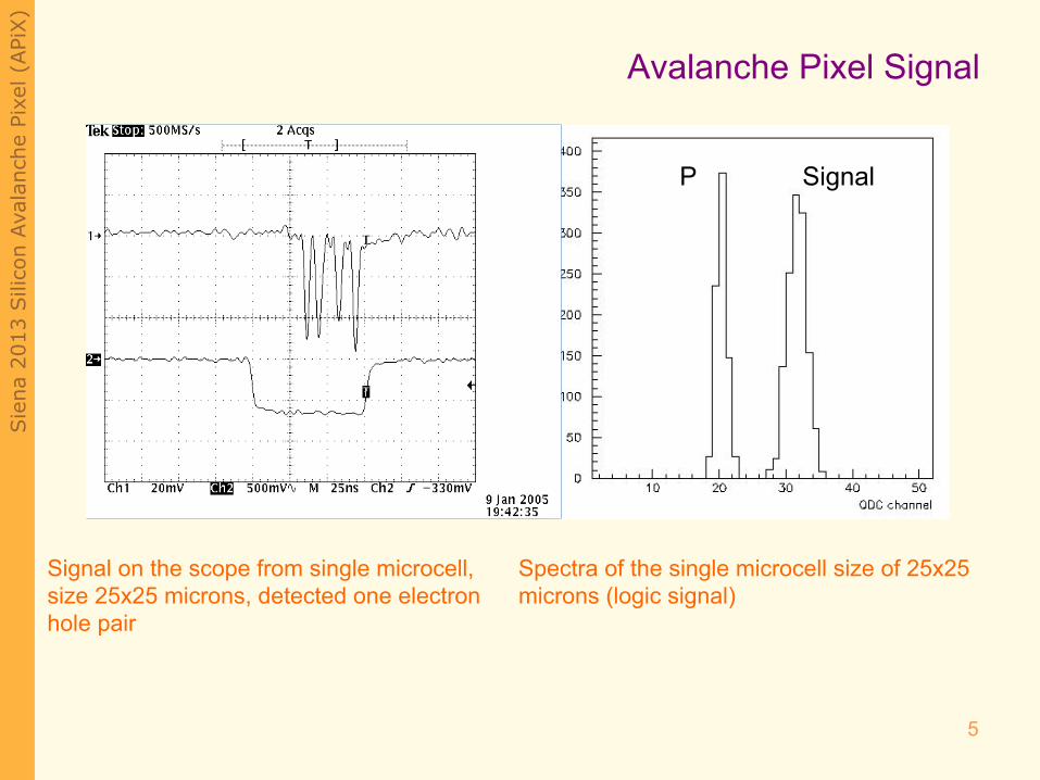
Spectra of the single microcell size of 25x25 microns (logic signal)
Signal on the scope from single microcell, size 25x25 microns, detected one electron hole pair
P Signal
Avalanche Pixel Signal
5
Sie
na 2
013
Sili
con
Aval
anch
e Pi
xel (
APi
X)
6
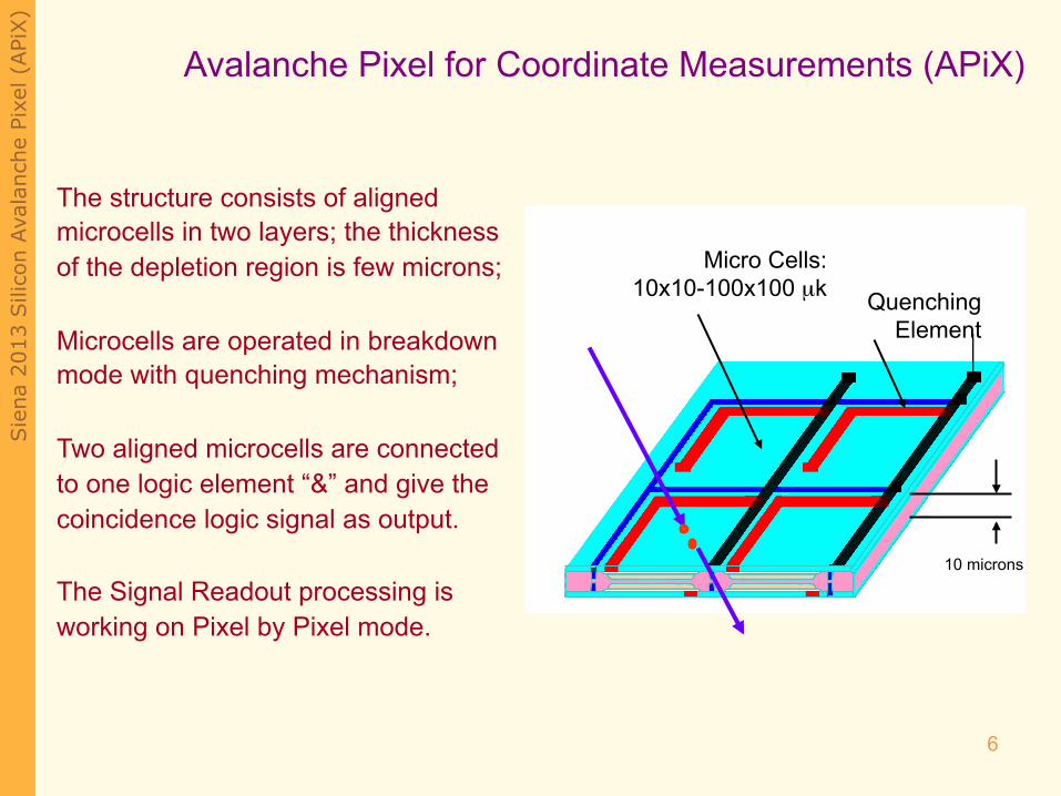
Avalanche Pixel for Coordinate Measurements (APiX)
The structure consists of aligned microcells in two layers; the thickness of the depletion region is few microns; Microcells are operated in breakdown mode with quenching mechanism; Two aligned microcells are connected to one logic element “&” and give the coincidence logic signal as output. The Signal Readout processing is working on Pixel by Pixel mode.
Micro Cells: 10x10-100x100 µk Quenching
Element
10 microns
Sie
na 2
013
Sili
con
Aval
anch
e Pi
xel (
APi
X)
7
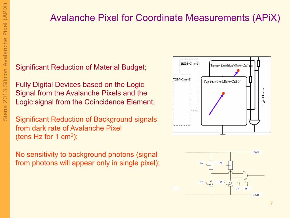
Avalanche Pixel for Coordinate Measurements (APiX)
Significant Reduction of Material Budget; Fully Digital Devices based on the Logic Signal from the Avalanche Pixels and the Logic signal from the Coincidence Element; Significant Reduction of Background signals from dark rate of Avalanche Pixel (tens Hz for 1 cm2); No sensitivity to background photons (signal from photons will appear only in single pixel);
26
12
126
112
36 37
GND
PWR
Sie
na 2
013
Sili
con
Aval
anch
e Pi
xel (
APi
X)
8
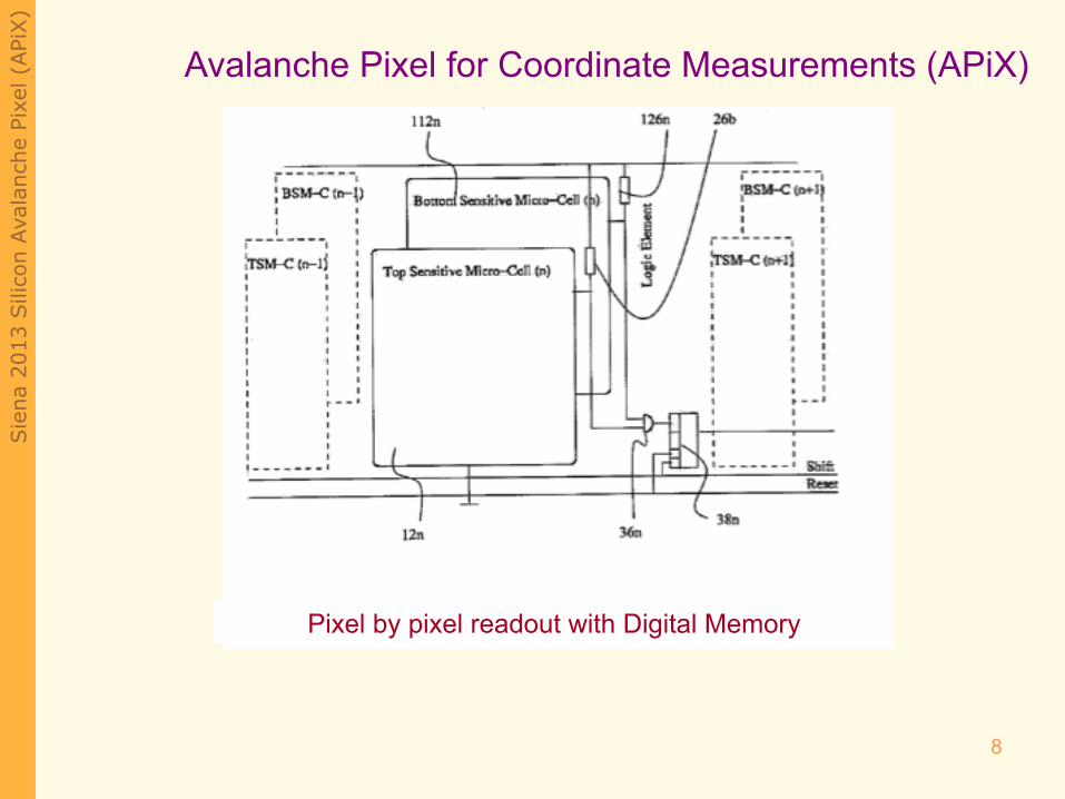
Avalanche Pixel for Coordinate Measurements (APiX)
Pixel by pixel readout with Digital Memory
Sie
na 2
013
Sili
con
Aval
anch
e Pi
xel (
APi
X)
9
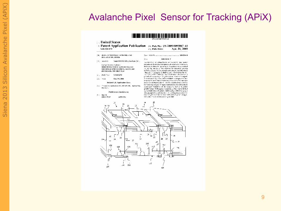
Avalanche Pixel Sensor for Tracking (APiX)
Sie
na 2
013
Sili
con
Aval
anch
e Pi
xel (
APi
X)
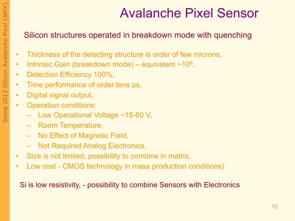
Avalanche Pixel Sensor
• Thickness of the detecting structure is order of few microns, • Intrinsic Gain (breakdown mode) – equivalent ~106, • Detection Efficiency 100%, • Time performance of order tens ps, • Digital signal output, • Operation conditions:
– Low Operational Voltage ~15-60 V, – Room Temperature, – No Effect of Magnetic Field, – Not Required Analog Electronics,
• Size is not limited, possibility to combine in matrix, • Low cost - CMOS technology in mass production conditions)
Silicon structures operated in breakdown mode with quenching
Si is low resistivity, - possibility to combine Sensors with Electronics
10
Sie
na 2
013
Sili
con
Aval
anch
e Pi
xel (
APi
X)
11
l For the sensors with high intrinsic gain, the detection of ionizing particles requires minimal material budget – the output signal does practically not depend on the sensitive material. Sensor thickness could be reduced to a few microns of the Silicon;
l Minimal effect due to low material budget, the Multiple Scattering is minimal and accordingly the precision of ionizing particle tracking is higher;
l The electronic noise does not really affect the output signal;
l The sensors are practically digital devices: there is no need for complicated analog front end electronics;
l The material of sensors is compatible with the standard electronics technology and the associated processing electronics will be implemented on the same chip together with sensors;
l No sensitivity to the background environment, as photons for instance;
Coordinate Measurement of Ionizing Particles
(new structure)
Sie
na 2
013
Sili
con
Aval
anch
e Pi
xel (
APi
X)
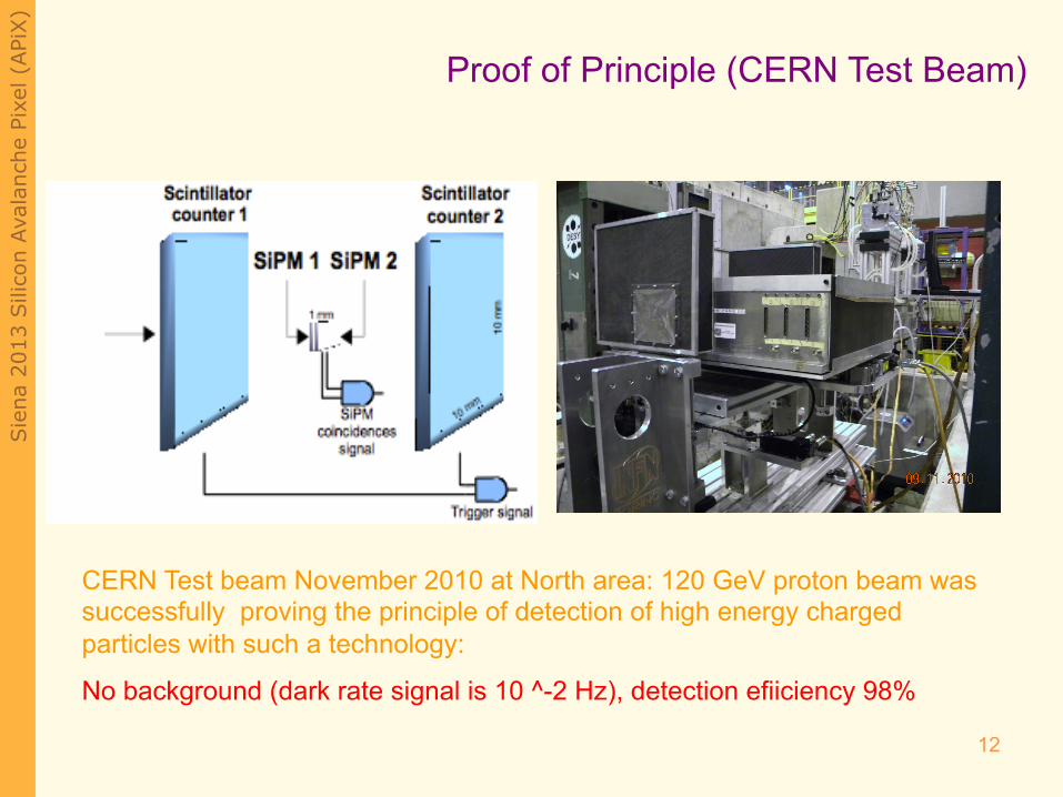
CERN Test beam November 2010 at North area: 120 GeV proton beam was successfully proving the principle of detection of high energy charged particles with such a technology:
No background (dark rate signal is 10 ^-2 Hz), detection efiiciency 98%
Proof of Principle (CERN Test Beam)
12
Sie
na 2
013
Sili
con
Aval
anch
e Pi
xel (
APi
X)
13
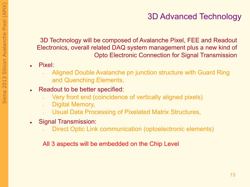
3D Advanced Technology
3D Technology will be composed of Avalanche Pixel, FEE and Readout Electronics, overall related DAQ system management plus a new kind of
Opto Electronic Connection for Signal Transmission l Pixel:
• Aligned Double Avalanche pn junction structure with Guard Ring and Quenching Elements,
l Readout to be better specified: • Very front end (coincidence of vertically aligned pixels) • Digital Memory, • Usual Data Processing of Pixelated Matrix Structures,
l Signal Transmission: • Direct Optic Link communication (optoelectronic elements) All 3 aspects will be embedded on the Chip Level
Sie
na 2
013
Sili
con
Aval
anch
e Pi
xel (
APi
X)
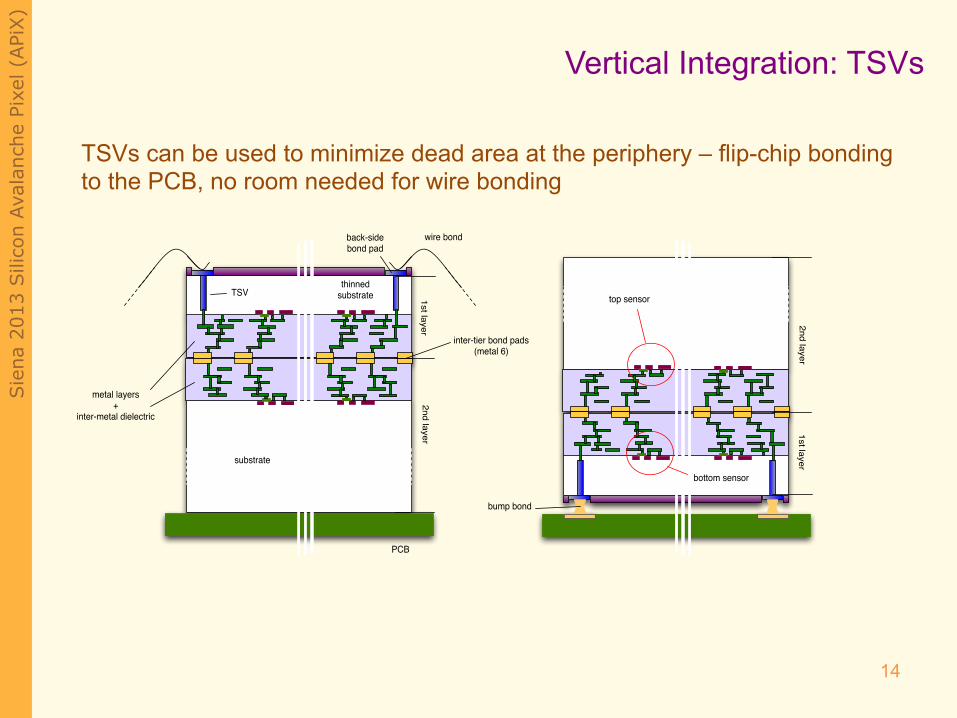
TSVs can be used to minimize dead area at the periphery – flip-chip bonding to the PCB, no room needed for wire bonding
1st layer2nd layer
2nd layer1st layer
inter-tier bond pads(metal 6)
metal layers +
inter-metal dielectric
wire bond
substrate
thinnedsubstrateTSV
bump bond
PCB
bottom sensor
top sensor
back-sidebond pad
Vertical Integration: TSVs
14
Sie
na 2
013
Sili
con
Aval
anch
e Pi
xel (
APi
X)
15
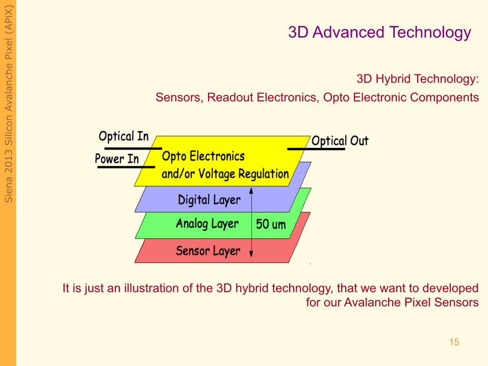
3D Advanced Technology
3D Hybrid Technology: Sensors, Readout Electronics, Opto Electronic Components
It is just an illustration of the 3D hybrid technology, that we want to developed for our Avalanche Pixel Sensors
Sie
na 2
013
Sili
con
Aval
anch
e Pi
xel (
APi
X)
• The development of an innovative position sensitive pixelated sensor to detect ionizing particles is presented. The Avalanche Pixel Sensor (APiX) is based on the vertical integration of avalanche pixels connected in pairs and operated in coincidence with embedded digital electronics on the chip.
• The APiX sensor addresses the need to minimize the material budget and related multiple scattering effects in tracking systems requiring a high spatial resolution in the presence of a large occupancy. The expected operation of the new sensor features low noise, low power consumption and suitable radiation tolerance.
• The APiX device provides on-chip digital information on the position of the impact coordinate of the impinging charged particle and can be seen as the building block of a modular system of pixelated arrays, implementing a sparsified readout.
• The technological challenge of the vertical integration of the device, under CMOS processes, will be performed.
Summary
Sie
na 2
013
Sili
con
Aval
anch
e Pi
xel (
APi
X)
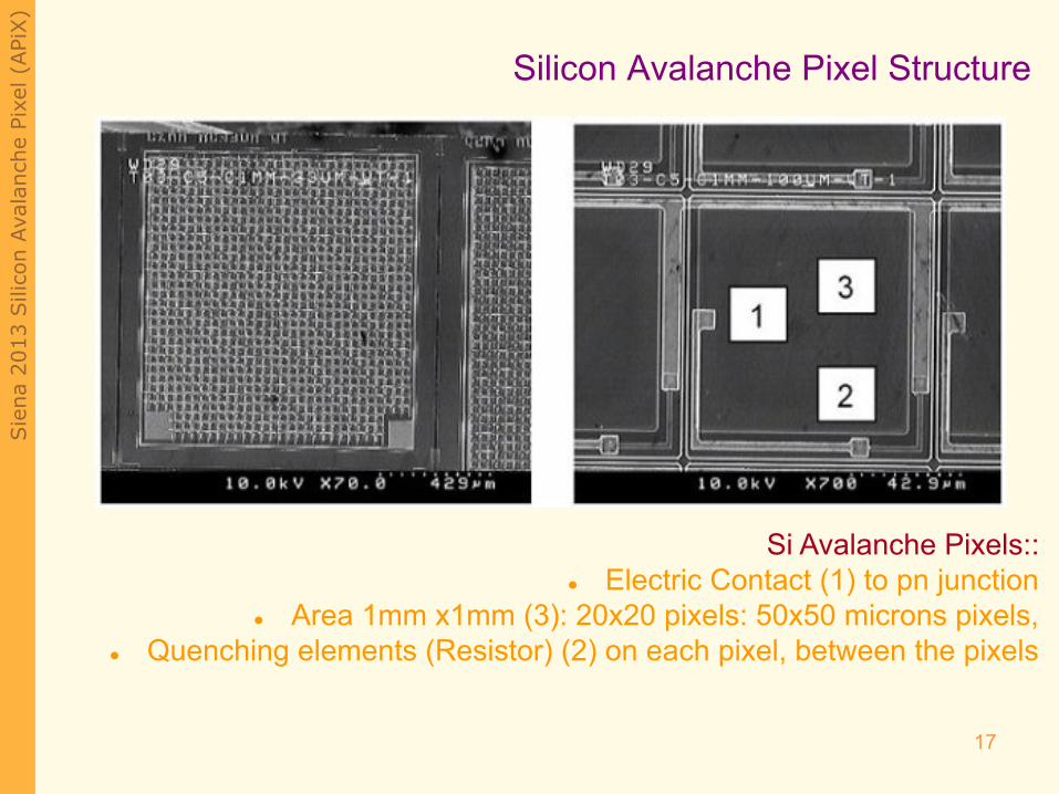
Si Avalanche Structure
Si Avalanche Pixels:: l Electric Contact (1) to pn junction
l Area 1mm x1mm (3): 20x20 pixels: 50x50 microns pixels, l Quenching elements (Resistor) (2) on each pixel, between the pixels
Silicon Avalanche Pixel Structure
17
Sie
na 2
013
Sili
con
Aval
anch
e Pi
xel (
APi
X)
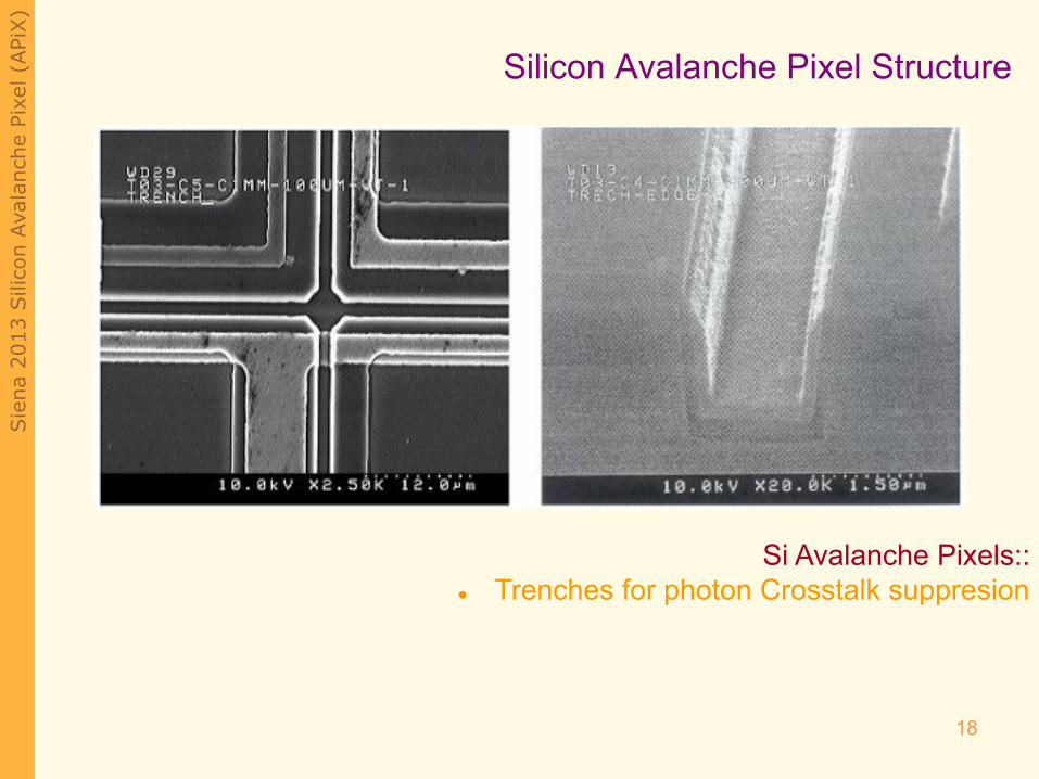
Si Avalanche Pixels:: l Trenches for photon Crosstalk suppresion
Silicon Avalanche Pixel Structure
18


![POSSIBLE VOLCANIC AVALANCHE DEPOSIT NORTH OF GALE … · slides on Mars (2 – 23) [10]. ... 100 meter/pixel mosaic (version 12) [13] were used for general mapping. • CTX digital](https://img.pdfslide.us/doc/110x75/5f19f5b8b21e86267516ddb0/possible-volcanic-avalanche-deposit-north-of-gale-slides-on-mars-2-a-23-10.jpg)