Embed Size (px)
Citation preview
MAT-VET-F 21027
Examensarbete 15 hpJuni 2021
Wireless Power Transfer in Cavity Resonator
Axel DjurbergFredrik ForsbergAnton LindLudvig Snihs
Teknisk- naturvetenskaplig fakultet UTH-enheten Besöksadress: Ångströmlaboratoriet Lägerhyddsvägen 1 Hus 4, Plan 0 Postadress: Box 536 751 21 Uppsala Telefon: 018 – 471 30 03 Telefax: 018 – 471 30 00 Hemsida: http://www.teknat.uu.se/student
Abstract
Wireless Power Transfer in Cavity Resonator
Axel Djurberg, Fredrik Forsberg, Anton Lind, Ludvig Snihs
The purpose of this paper is to achieve wireless power transfer inside a resonating cavity, and thereby apply this to charge batteries. The idea is to convert radio frequency waves into direct current, which can charge the batteries. This was done by creating an LC-antenna, which in turn was connected to a rectifier. A data logger was also built, this to be able to read and log the power within the cavity to examine its power distribution. Because of COVID-19 restrictions, access to laboratory and equipment was limited. Due to this, smaller experiments where performed to make sure that all parts worked as intended before trying to perform tests inside the cavity resonator. The results were varied, some favorable, some not. However, all experiments gave insight and further understanding on the issue.
The cavity operations had varied results. The data logger was able to pick up, at most, 7.6 % of the power output by the function generator. However, some problems arose with the rectifier which resulted in it not working for higher frequencies. Though, it was capable of rectifying RF signals at lower frequencies from a function generator, which was used to charge a battery. Consequently, there was no charging of batteries inside the cavity. However, three dimensional wireless power transfer was achieved. With some improvements to the current designs, the main goal could be accomplished.
Tryckt av: UppsalaISSN: 1401-5757, MAT-VET-F 21027Examinator: Martin SjödinÄmnesgranskare: Chao XuHandledare: Dragos Dancila

Populärvetenkaplig sammanfattningPå senare år har en snabb utveckling inom trådlös laddning skett, och idag är det ett välkäntkoncept som används för att ladda mobiltelefoner, smart-klockor och dylikt. Det finns flerafördelar med att byta ut den klassiska sladd-laddaren mot en trådlös platta, den främstaär bekvämlighet. För att ytterligare avancera konceptet av bekvämlighet har forskning ochutveckling av 3D-laddning förts fram; där man, i princip, kan lägga en elektronisk apparatvart som helst inuti en speciellt konstruerad låda, och detta föremål ska då laddas. För attbidra till utvecklingen ska vi därmed undersöka detta koncept, och i sin tur försöka uppnå3D-laddning.
Grundkonceptet som ligger bakom 3D-laddning är en omvandling av radiofrekvensvågor (RF) till likström(DC). Första steget är att man, i en metallåda, skickar in RF-vågor som för en viss frekvens blir ståendevågor. Frekvensen för RF vågor brukar ligga mellan 20kHz till 300GHz och just den frekvensen som behövsför att uppnå stående vågor är direkt beroende av dimensionerna på lådan. Man brukar kalla detta för attvågorna hamnar i resonans, och det är essentiellt för att uppnå en hög effektivitet.
Nästkommande steg är att fånga upp vågorna inuti lådan och omvandla dessa till likström, som kan användasför laddning. För att fånga upp RF vågorna används, på liknande sätt som för 2D laddning, en LC-krets (enkrets bestående av en spole och en kondensator). Spolen fångar upp vågorna och det induceras då växelström(AC) i LC-kretsen som sedan, med en likriktare, kan göras om till en stabil likström. Då LC-kretsen har enegen resonansfrekvens bör den konstrueras så att den får samma resonansfrekvens som lådan.
Det bör poängteras att bytet mellan icke trådlös och trådlös laddning ofta kommer med förbehåll. Framförallt att effektöverföringen blir sämre. Detta gäller till ännu större grad för 3D laddning då det är svårt attfånga upp majoriteten av energin som finns i lådan, speciellt om spolen behöver vara liten. Dock en uppoffringsom kan göras om effektförlusten är mindre betydande än den ökade bekvämligheten av 3D laddning.
Ett exempel när bekvämlighet kan vara av högre prioriterat än bra effektöverföring är vid laddning avväldigt små drönare. Drönare har blivit mer och mer populärt de senaste åren och således har utvecklingenav drönare också ökat. Forskare och företag har till och med börjat utveckla drönare som är små som bin.Det finns flera användningsområden för dessa typer av drönare; agera som pollinerare om bi-populationenskulle bli låg, söka igenom olycksplatser, leta efter människor, med mera. Men, när man har något som ärså litet och troligtvis av hög kvantitet som behöver laddas, kan det vara bökigt och tidskrävande att laddavarje enskild drönare med sladd. Vi tänker att detta skulle vara en perfekt applikation för 3D laddning. Attman kan konstruera en resonanslåda med flera brickor staplade ovanpå varandra där drönarna kan flyga inav sig själva och ladda när de har lågt batteri, som en bikupa.
Ett flertal experiment, tester och simuleringar har gjorts för att vidare förstå och klargöra varje steg utaveffektöverföring i ett 3D rum. En resonerande låda exciterad med 433 MHz och en LC-krets plockade uppmaximalt 7.6% av källans utsända effekt. Detta mättes med en konstruerad effekt detekterare datalogger.Vidare konstruerades en likriktare som dock inte fungerande för så pass höga frekvensker, men som ändålyckades ladda ett batteri med en funktionsgenerator som input (istället för en resonanslåda och LC-krets).
3
Contents1 Introduction 6
1.1 Problem description . . . . . . . . . . . . . . . . . . . . . . . . . . . . . . . . . . . . . . . . . 6
2 Theory 82.1 Resonator . . . . . . . . . . . . . . . . . . . . . . . . . . . . . . . . . . . . . . . . . . . . . . . 8
2.1.1 Rectangular Waveguide . . . . . . . . . . . . . . . . . . . . . . . . . . . . . . . . . . . 82.1.2 Rectangular waveguide cavity resonators . . . . . . . . . . . . . . . . . . . . . . . . . . 10
2.2 ISM band . . . . . . . . . . . . . . . . . . . . . . . . . . . . . . . . . . . . . . . . . . . . . . . 122.3 Impedance matching . . . . . . . . . . . . . . . . . . . . . . . . . . . . . . . . . . . . . . . . . 122.4 Coupling coefficient . . . . . . . . . . . . . . . . . . . . . . . . . . . . . . . . . . . . . . . . . . 122.5 LC-circuits . . . . . . . . . . . . . . . . . . . . . . . . . . . . . . . . . . . . . . . . . . . . . . 132.6 Construction of an LC-receiver . . . . . . . . . . . . . . . . . . . . . . . . . . . . . . . . . . . 15
2.6.1 Circular loop inductor . . . . . . . . . . . . . . . . . . . . . . . . . . . . . . . . . . . . 152.6.2 Coil inductor . . . . . . . . . . . . . . . . . . . . . . . . . . . . . . . . . . . . . . . . . 15
2.7 Batteries . . . . . . . . . . . . . . . . . . . . . . . . . . . . . . . . . . . . . . . . . . . . . . . . 162.7.1 Battery capacity . . . . . . . . . . . . . . . . . . . . . . . . . . . . . . . . . . . . . . . 162.7.2 Charging and discharging . . . . . . . . . . . . . . . . . . . . . . . . . . . . . . . . . . 16
2.8 Arduino . . . . . . . . . . . . . . . . . . . . . . . . . . . . . . . . . . . . . . . . . . . . . . . . 172.9 Vector Network Analyzer . . . . . . . . . . . . . . . . . . . . . . . . . . . . . . . . . . . . . . 18
3 Method 193.1 Cavity Resonator . . . . . . . . . . . . . . . . . . . . . . . . . . . . . . . . . . . . . . . . . . . 19
3.1.1 Resonance frequency . . . . . . . . . . . . . . . . . . . . . . . . . . . . . . . . . . . . . 193.1.2 COMSOL simulations . . . . . . . . . . . . . . . . . . . . . . . . . . . . . . . . . . . . 193.1.3 Construction of the cavity . . . . . . . . . . . . . . . . . . . . . . . . . . . . . . . . . . 21
3.2 RF-to-DC converter . . . . . . . . . . . . . . . . . . . . . . . . . . . . . . . . . . . . . . . . . 213.2.1 Rectifier . . . . . . . . . . . . . . . . . . . . . . . . . . . . . . . . . . . . . . . . . . . . 22
3.3 Battery testing . . . . . . . . . . . . . . . . . . . . . . . . . . . . . . . . . . . . . . . . . . . . 233.3.1 Choice of battery . . . . . . . . . . . . . . . . . . . . . . . . . . . . . . . . . . . . . . . 233.3.2 Discharge . . . . . . . . . . . . . . . . . . . . . . . . . . . . . . . . . . . . . . . . . . . 243.3.3 Charge . . . . . . . . . . . . . . . . . . . . . . . . . . . . . . . . . . . . . . . . . . . . 25
3.4 Data logger . . . . . . . . . . . . . . . . . . . . . . . . . . . . . . . . . . . . . . . . . . . . . . 263.4.1 RF Power detector . . . . . . . . . . . . . . . . . . . . . . . . . . . . . . . . . . . . . . 263.4.2 Construction and testing . . . . . . . . . . . . . . . . . . . . . . . . . . . . . . . . . . 283.4.3 CAD and 3D-printing . . . . . . . . . . . . . . . . . . . . . . . . . . . . . . . . . . . . 29
3.5 2D testing . . . . . . . . . . . . . . . . . . . . . . . . . . . . . . . . . . . . . . . . . . . . . . . 303.5.1 Resonance frequency of LC-circuits . . . . . . . . . . . . . . . . . . . . . . . . . . . . . 313.5.2 2D testing and logging with data logger . . . . . . . . . . . . . . . . . . . . . . . . . . 32
3.6 Cavity operation . . . . . . . . . . . . . . . . . . . . . . . . . . . . . . . . . . . . . . . . . . . 333.6.1 LC-receiver . . . . . . . . . . . . . . . . . . . . . . . . . . . . . . . . . . . . . . . . . . 333.6.2 Measurement of cavity resonance frequency . . . . . . . . . . . . . . . . . . . . . . . . 343.6.3 Data logging inside cavity . . . . . . . . . . . . . . . . . . . . . . . . . . . . . . . . . . 35
4 Results and discussion 374.1 Primary testings . . . . . . . . . . . . . . . . . . . . . . . . . . . . . . . . . . . . . . . . . . . 37
4.1.1 RF-DC converter . . . . . . . . . . . . . . . . . . . . . . . . . . . . . . . . . . . . . . . 374.1.2 Battery discharge . . . . . . . . . . . . . . . . . . . . . . . . . . . . . . . . . . . . . . . 394.1.3 Battery recharge . . . . . . . . . . . . . . . . . . . . . . . . . . . . . . . . . . . . . . . 404.1.4 LC-receiver . . . . . . . . . . . . . . . . . . . . . . . . . . . . . . . . . . . . . . . . . . 404.1.5 2D testing and data logging . . . . . . . . . . . . . . . . . . . . . . . . . . . . . . . . . 43
4
4.2 Operating in cavity . . . . . . . . . . . . . . . . . . . . . . . . . . . . . . . . . . . . . . . . . . 44
5 Conclusion 46
Appendix A: Code 49Appendix A.1: Charge/Discharge . . . . . . . . . . . . . . . . . . . . . . . . . . . . . . . . . . . . 49Appendix A.2: Data logger . . . . . . . . . . . . . . . . . . . . . . . . . . . . . . . . . . . . . . . 51
Appendix B: Data Sheets 53Appendix B.1: ZX47-40LN-S+ RF Power Detector . . . . . . . . . . . . . . . . . . . . . . . . . . 53Appendix B.2: 1N5817 Diode . . . . . . . . . . . . . . . . . . . . . . . . . . . . . . . . . . . . . . 67
5
1 IntroductionVisible light and the vicious gamma rays are both electromagnetic waves, but they differ in frequency. Radiofrequency (RF) waves are signals with a range from about 20 kHz to 300 GHz. These are mainly used fortransporting information through the air from a transmitter to a receiver. Examples are radio FM signalsand WiFi. The transportation implies a lot of power loss, which is not a major problem when informationis exchanged [1].
Wireless power transfer was first discovered by Tesla in 1891, where he the following years kept developingthe idea [2]. More recently, inductive charging is becoming the standard in e.g. mobile phone and headphonecharging. This can be seen as a 2D charging where the transmitter and receiver has to be rather close.
However, 3D wireless power transfer is a relatively new concept that is not widely used, because of theproblem with power losses at great distances. Wireless power transfer could potentially remove the need forcables and batteries in many applications.
By resonant coupling, using an LC-circuit to resonate at the operating frequency, the transferred power canbe increased. Furthermore, by using a cavity resonator, i.e. a hollow geometry with walls of conductivematerial where the RF signal and its energy is stored, the power transfer efficiency can drastically increase.Operating the cavity at a certain frequency will give raise to standing electromagnetic waves. Energy canbe harvested from the magnetic waves by inductive coupling.
Previous research utilizing cavity resonators has used it with animal experiments, where rats with a receiverimplant lived inside a cavity [3]. Others have charged multiple devices simultaneously inside the cavity [4].The latter application will be the focus of this paper, as the technique of charging multiple drones in threedimensional space is sought after. The application of drones has drastically increased in recent years. Oneexample is Prime Air, a delivery system using drones [5]. However, the charging of these drones are donevia cables or 2D charging pads, whilst in this paper we propose a technique where multiple drones can becharged simultaneously in 3D space.
The main advantage of opting for 3D-charging, instead of wired, is convenience. In the case of drones, thisconvenience can lead to greater automatization as the drones can be programmed to conveniently fly into thecavity by themselves. Instead of having multiple cords which need to be plugged in to each drone. One couldargue that 2D-charging would suffice for this purpose, but that would require a great number of separatecharging pads, whereas only one cavity would be needed for 3D-charging. Regardless if 2D-charging mightbe a better option today, from an efficiency standpoint, further advancements in the future might make 3Dpower transfer more economic and environmentally friendly than current techniques.
1.1 Problem descriptionThe aim of this work is to create a wireless power transfer system in 3D space using a cavity resonator.
The final goal is to simultaneously charge at least two rechargeable AAA-NiMH batteries within the cavity.This shall be done with a small receiver. An additional goal is to develop a RF power detecting data loggerto be able to read and log the power within the cavity to examine its power distribution. Furtermore, thepower transfer efficiency (PTE) from transmitting source to the receiving antenna is to be calculated.
To achieve this, smaller sub goals are defined as the following:
− Build a cavity resonator made of aluminum.
− Build a resonant LC-circuit as an antenna that can couple to the magnetic fields of the cavity.
− Construct a RF-to-DC rectifier that converts the received signal from the antenna to DC signal.
− Examine the discharge and recharge curves of the chosen batteries.
6

− Construct a RF power detector data logger to examine the characteristics of the cavity, and comparethe findings to COMSOL simulations.
To make sure that the constructions of the aforementioned sub goals work as intended, smaller experimentswill be performed before testing them inside the cavity resonator.
7
2 Theory
2.1 Resonator2.1.1 Rectangular Waveguide
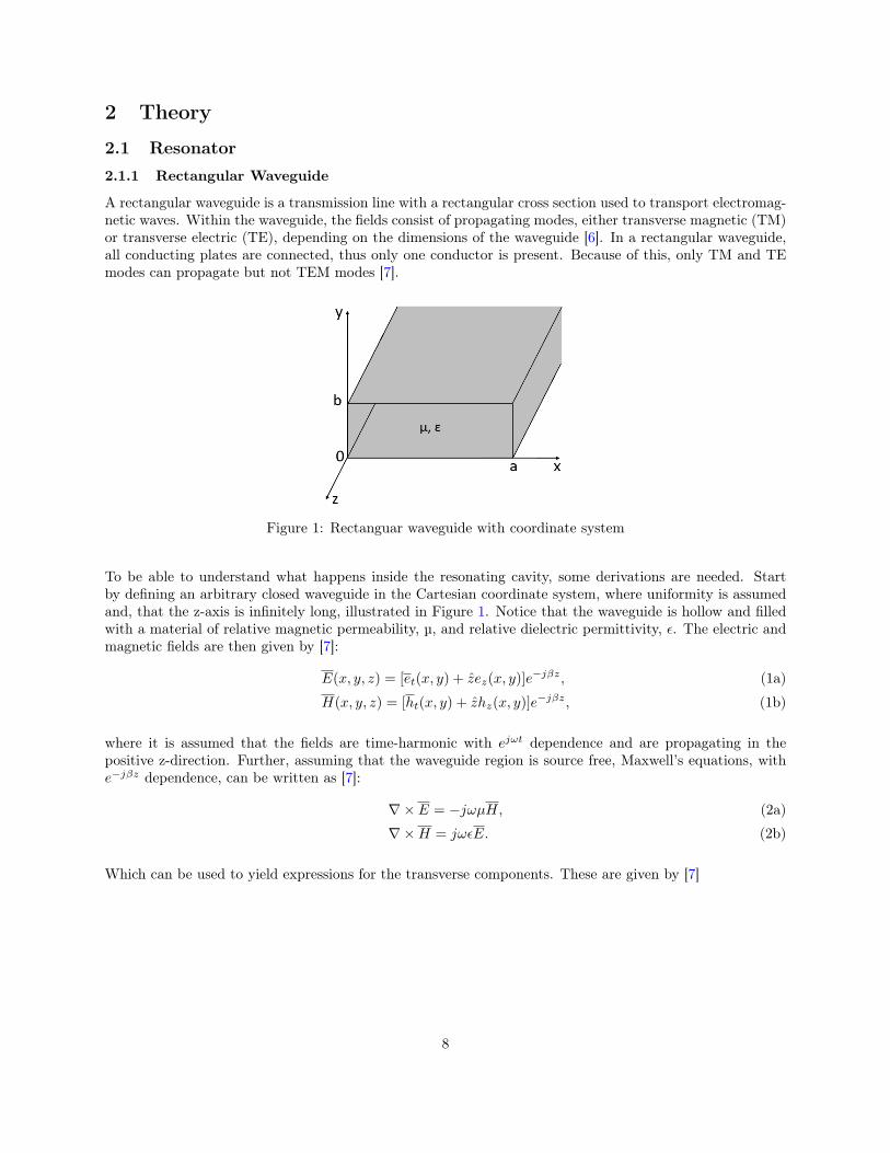
A rectangular waveguide is a transmission line with a rectangular cross section used to transport electromag-netic waves. Within the waveguide, the fields consist of propagating modes, either transverse magnetic (TM)or transverse electric (TE), depending on the dimensions of the waveguide [6]. In a rectangular waveguide,all conducting plates are connected, thus only one conductor is present. Because of this, only TM and TEmodes can propagate but not TEM modes [7].
Figure 1: Rectanguar waveguide with coordinate system
To be able to understand what happens inside the resonating cavity, some derivations are needed. Startby defining an arbitrary closed waveguide in the Cartesian coordinate system, where uniformity is assumedand, that the z-axis is infinitely long, illustrated in Figure 1. Notice that the waveguide is hollow and filledwith a material of relative magnetic permeability, µ, and relative dielectric permittivity, ε. The electric andmagnetic fields are then given by [7]:
E(x, y, z) = [et(x, y) + zez(x, y)]e−jβz, (1a)
H(x, y, z) = [ht(x, y) + zhz(x, y)]e−jβz, (1b)
where it is assumed that the fields are time-harmonic with ejωt dependence and are propagating in thepositive z-direction. Further, assuming that the waveguide region is source free, Maxwell’s equations, withe−jβz dependence, can be written as [7]:
∇× E = −jωµH, (2a)
∇×H = jωεE. (2b)
Which can be used to yield expressions for the transverse components. These are given by [7]
8
Hx =j
ω2µε− β2
(ωε∂Ez∂y− β ∂Hz
∂x
), (3a)
Hy = − j
ω2µε− β2
(ωε∂Ez∂x− β ∂Hz
∂y
), (3b)
Ex = − j
ω2µε− β2
(β∂Ez∂x
+ ωµ∂Hz
∂y
), (3c)
Ey =j
ω2µε− β2
(β∂Ez∂y− ωµ∂Hz
∂x
). (3d)
where β is the propagation constant of the TE and TM waves.
Transverse electric waves
Transverse electric waves are defined by when Ez is zero, and Hz is non-zero. Start by solving the Helmholtzwave equation for Hz, namely
∇2Hz(x, y, z) + ω2µεHz(x, y, z) = 0. (4)
Since e−jωz dependence is assumed, the third-dimensional Helmholtz can be reduced to a two-dimensionalproblem, i.e.
∇2Hz(x, y) + (ω2µε− β2)Hz(x, y) = 0, (5)
since ∂2Hz/∂z2 = −β2. This wave-equation can be solved by eigenfunction expansion and the utilization
of (3), which is especially trivial because of the homogeneous Dirichlet boundary conditions. Consequently,the final solution is given by [7]
Hz = Am,n cos(mπx
a) cos(
nπy
b)e−jωz. (6)
With this expression for Hz, all components of the TE-waves can be solved using (3). See Table 1 for allcomponents.
Transverse magnetic waves
Transverse magnetic waves are defined by when Hz is zero, and Ez is non-zero. Similarly to the case of TE-waves, we solve the Helmholtz wave equation. This time for Ez. The only difference is that the boundaryconditions can be applied directly to the general solution, without the need of utilizing (3). The final solutionis therefore given by [7]
Ez = Bm,n sin(mπx
a) sin(
nπy
b)e−jωz. (7)
With this expression for Ez, all components of the TM-waves can be solved using (3). See Table 1 for allcomponents.
9
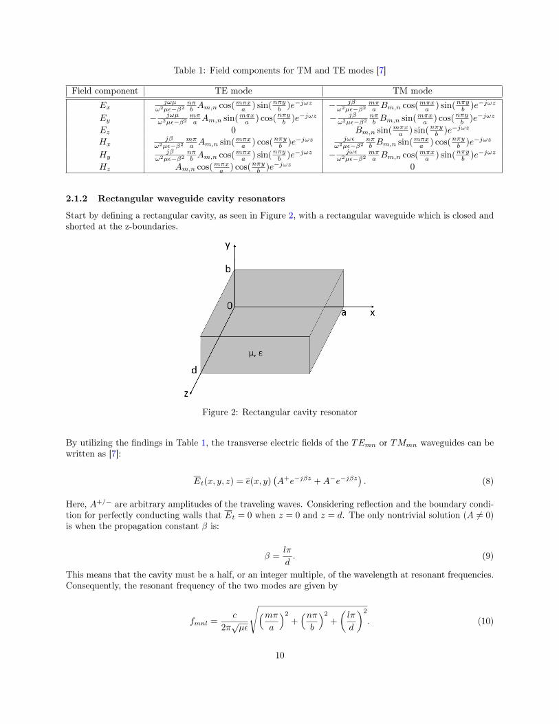
Table 1: Field components for TM and TE modes [7]
Field component TE mode TM modeEx
jωµω2µε−β2
nπb Am,n cos(mπxa ) sin(nπyb )e−jωz − jβ
ω2µε−β2mπa Bm,n cos(mπxa ) sin(nπyb )e−jωz
Ey − jωµω2µε−β2
mπa Am,n sin(mπxa ) cos(nπyb )e−jωz − jβ
ω2µε−β2nπb Bm,n sin(mπxa ) cos(nπyb )e−jωz
Ez 0 Bm,n sin(mπxa ) sin(nπyb )e−jωz
Hxjβ
ω2µε−β2mπa Am,n sin(mπxa ) cos(nπyb )e−jωz jωε
ω2µε−β2nπb Bm,n sin(mπxa ) cos(nπyb )e−jωz
Hyjβ
ω2µε−β2nπb Am,n cos(mπxa ) sin(nπyb )e−jωz − jωε
ω2µε−β2mπa Bm,n cos(mπxa ) sin(nπyb )e−jωz
Hz Am,n cos(mπxa ) cos(nπyb )e−jωz 0
2.1.2 Rectangular waveguide cavity resonators
Start by defining a rectangular cavity, as seen in Figure 2, with a rectangular waveguide which is closed andshorted at the z-boundaries.
Figure 2: Rectangular cavity resonator
By utilizing the findings in Table 1, the transverse electric fields of the TEmn or TMmn waveguides can bewritten as [7]:
Et(x, y, z) = e(x, y)(A+e−jβz +A−e−jβz
). (8)
Here, A+/− are arbitrary amplitudes of the traveling waves. Considering reflection and the boundary condi-tion for perfectly conducting walls that Et = 0 when z = 0 and z = d. The only nontrivial solution (A 6= 0)is when the propagation constant β is:
β =lπ
d. (9)
This means that the cavity must be a half, or an integer multiple, of the wavelength at resonant frequencies.Consequently, the resonant frequency of the two modes are given by
fmnl =c
2π√µε
√(mπa
)2+(nπb
)2+
(lπ
d
)2
. (10)
10
Here,m, n, l, are the number of variations in the standing wave patterns in the x, y, z - directions respectively.c is the speed of light. To determine the dominant mode, the dimensions of the cavity must be known.Assuming commonly dimensions for a resonating cavity, that is b < a < d, the dominant mode is the TE101
mode, i.e. the one with lowest resonant frequency. This corresponds to a cavity with length (z-direction)λ/2. Notice that if a = d the TE101 and TE011 will have the same resonance frequency [7].
Each mode of the cavity resonator has a distinct standing wave pattern at their resonance frequency. Whenthe operating frequency equals the resonance frequency of a mode, this mode will be the operating one andthe distribution of the H-field and E-field will depend on this mode [8].
Steady state and Quality factor Q
When exciting a resonating cavity with electromagnetic waves, there is a maximum amount of energy thatcan be stored inside the cavity, meaning there will be an equilibrium steady state. When the maximumenergy is reached, the power pumped into the cavity mainly goes into wall heating [9].
The quality factor Q of a resonant circuit (see section 2.5) is defined as:
Q = ωAverage energy storedenergy loss / second
(11)
A cavity resonator can be modeled as a resonant circuit, which means that the Q-factor is a measure of itslosses [7]. Therefore, a highly conductive material is of interested when constructing a cavity resonator tomaximize the unloaded Q-factor, since it results in a maximized power transfer efficiency [3].
RF excitation
To excite a cavity resonator with RF-signals, a linear probe antenna can be used. The probe should bemounted where the E-field is strongest. Furthermore, the length should be parallel with the E-fields. Thenthe probe drives the current, thus the E-field is in the same direction as the cavity’s E-field. Consequently,the probe and cavity couples strongly and maximizes efficiency [10, 11].
Cavity Perturbation
The electromagnetic fields inside a cavity changes when the cavity is perturbed. In other words, when thecavity is altered by changing its size, or adding a (di)electric material, the fields change. Cavity resonatorsare often modified this way in practical applications. For instance, by inserting a metallic screw into thecavity, the resonance frequency will be lowered and thus tuned depending on the screw size. One can assumethat the field distribution changes a tiny amount from the unperturbed fields [7, 12].
Multimode resonance
Multimode resonance occures when several modes are being excited in a cavity. This is commonly used inhigh frequency applications such as microwave ovens. To realize multimode resonance, the dimensions of thecavity has to be at least two times larger than the operating frequency wavelength. An excited mode from(10), e.g. the TE324-mode, will have a lot of maximums and minimums within the cavity. Due to this, theuniformity of the distribution is poor, since just by moving a small distance you can move from a maximumto a minimum. By using a varying excitation frequency one can excite many different modes. For instancea cavity of dimensions 30 x 35 x 25[cm] with a varying frequency of 2450 ± 25 MHz will excite 6 modes.Doubling the dimensions, nearly 40 modes will be excited. Excitation of many modes will produce a cavitywith more uniform field distribution as the probability of a maximum is rather large at any location insidethe cavity [8].
11
2.2 ISM bandThe ISM band are parts of the frequency spectrum that are internationally reserved for specific industrial,scientific or medicinal applications, hence the name ISM. The ISM band is needed since these applicationsmay cause electromagnetic interference, which can disrupt radio- and telecommunication that operate in thesame frequency. The frequency allocation is defined in the Radio Regulations, which are an appendix to theTelecommunications Convention established by the International Telecommunication Union (ITU), which inturn is a body within the UN [13].
Note that ISM electronics should be able to tolerate interference stemming from other instruments thatbelong in the same frequency. Licensed users for each ISM band differs from region to local acceptance, e.g.amateur service (also known as ham radio) is assigned to 430-440 MHz in region 1 which includes Europe,Africa and most of northern Asia [14]. When designing electronic devices that operates in the MHz-rangeand above, it is therefore important to know which frequency is available and which ones are not.
2.3 Impedance matchingThe maximum power-transfer theorem states that, to achieve the best possible power transfer efficiency(PTE) from the source to the load, it is necessary to impedance match the two. More specifically, theimpedance of the source, Zsource, must be matched to the impedance of the load, Zload, accordingly:Zsource = Z∗
load, where Z is the impedance and ∗ denotes the complex conjugate. Hence, if Zsource = R+jXthen Zload = R − jX is required to achieve maximum PTE. If the load is purely resistive but the sourceis reactive, a reactance X with a negative sign must be added at the load. Note that since X is frequencydependent, impedance matching only works for one frequency in most cases [15]. This is analogous to me-chanics, where one object colliding with another object will transfer the highest amount of kinetic energy ifthey have the same amount of mass. In this type of cavity 3D wireless power transfer, impedance matchingcan be applied in practically every interconnected stage; the probe, the cavity, the receiver and the batteryall have individual impedance that can be matched to each other.
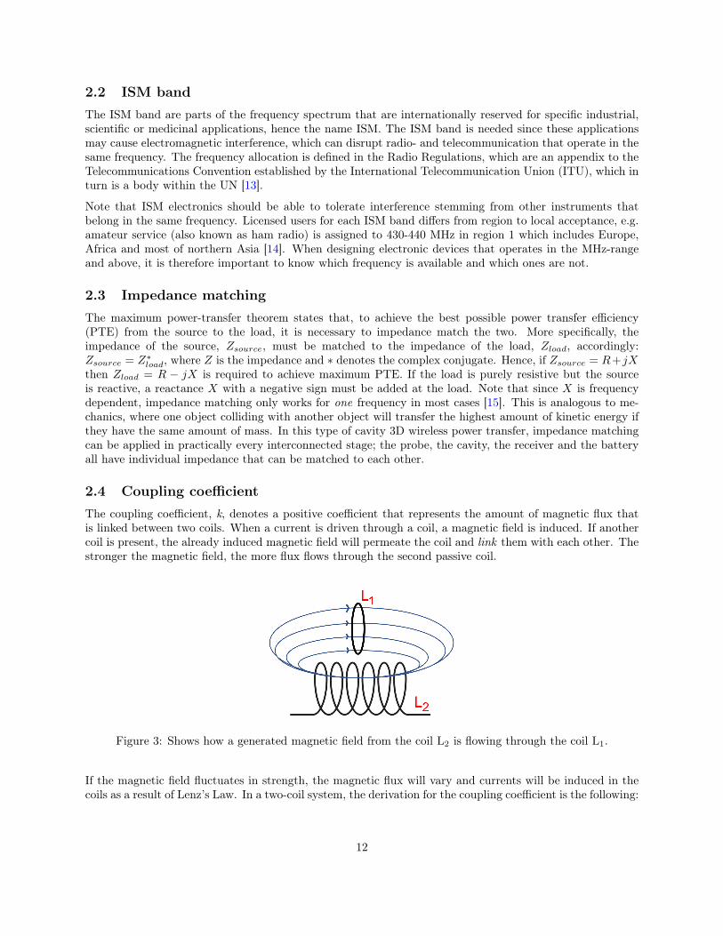
2.4 Coupling coefficientThe coupling coefficient, k, denotes a positive coefficient that represents the amount of magnetic flux thatis linked between two coils. When a current is driven through a coil, a magnetic field is induced. If anothercoil is present, the already induced magnetic field will permeate the coil and link them with each other. Thestronger the magnetic field, the more flux flows through the second passive coil.
Figure 3: Shows how a generated magnetic field from the coil L2 is flowing through the coil L1.
If the magnetic field fluctuates in strength, the magnetic flux will vary and currents will be induced in thecoils as a result of Lenz’s Law. In a two-coil system, the derivation for the coupling coefficient is the following:
12
Consider L1 and L2 as shown in Figure 3. If a current I1 and I2 flows through the two coils the followingholds:
L1 =N1φ1I1
& L2 =N2φ2I2
.
Where φ is the magnetic flux through the coil due to the current flowing in the coil itself. The mutualinductance is then defined as
M =N2φ12I1
or M =N1φ21I2
=N1kφ2I2
.
Multiplying the two different expressions for mutual inductance gives:
M ×M =N1kφ2I2
N2kφ1I1
,
M2 = k2N1φ1I1
N2φ2I2
= k2L1L2,
M = k√L1L2. (12)
Since a higher mutual inductance will increase the induced current through a second loop, a highly coupledpair of coils is beneficial. The coupling coefficient is often defined as 0 < k < 1, so in a case where k = 1, thetwo coils are magnetically tightly coupled whereas if k = 0, suggest them to be magnetically isolated fromeach other [16].
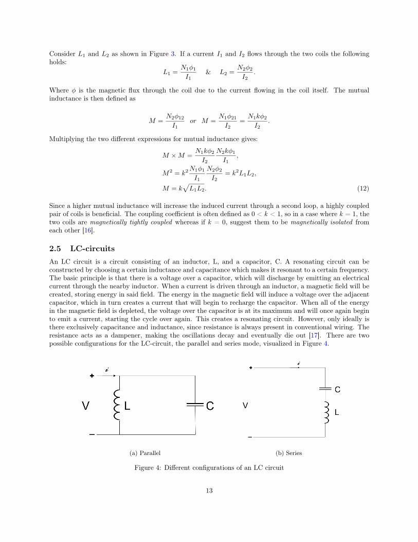
2.5 LC-circuitsAn LC circuit is a circuit consisting of an inductor, L, and a capacitor, C. A resonating circuit can beconstructed by choosing a certain inductance and capacitance which makes it resonant to a certain frequency.The basic principle is that there is a voltage over a capacitor, which will discharge by emitting an electricalcurrent through the nearby inductor. When a current is driven through an inductor, a magnetic field will becreated, storing energy in said field. The energy in the magnetic field will induce a voltage over the adjacentcapacitor, which in turn creates a current that will begin to recharge the capacitor. When all of the energyin the magnetic field is depleted, the voltage over the capacitor is at its maximum and will once again beginto emit a current, starting the cycle over again. This creates a resonating circuit. However, only ideally isthere exclusively capacitance and inductance, since resistance is always present in conventional wiring. Theresistance acts as a dampener, making the oscillations decay and eventually die out [17]. There are twopossible configurations for the LC-circuit, the parallel and series mode, visualized in Figure 4.
(a) Parallel (b) Series
Figure 4: Different configurations of an LC circuit
13
In both configurations, resonance occurs when, for a given frequency, the reactants of the inductor andcapacitor are equal but opposite in sign. Hence:
ωL =1
ωC
ω = ω0 =1√LC
(13)
This is defined as the resonant angular frequency. Studying the impedance’s of these configurations gives anidea of how these can be used in a circuit.
Impedance of a series LC-circuit
The total impedance is given by:
Z = ZL + ZC
= jωL+1
jωC
= j(ω2LC − 1
ωC).
By using (13) one obtains:
Z = jL(ω2 − ω0
2
ω). (14)
From (14), one deduces that at the resonance frequency there is zero impedance, so a series LC-circuit willact as a band-pass filter if connected in series with a load, having little to no impact on the voltage loss ina voltage division.
Impedance of a parallel LC-circuit
We perform the same analysis as for the series circuit. The total impedance is given by:
Z =ZLZCZL + ZC
=jωL 1
jωC
jωL+ 1jωC
= −j ωL
ω2LC − 1.
Using the resonant angular frequency (13), we obtain:
Z = −j( 1
C)
ω
ω2 − ω02. (15)
From (15), it is concluded that the impedance goes to infinity if driven by a voltage source at resonatingfrequency. Hence, a parallel LC-circuit connected in series with a load will also act as a band-pass filter.
14
LC-circuits in WPT
A resonating circuit can be used to couple to a distant voltage source, thus enabling wireless power trans-mission. This phenomenon is made possible by means of mutual inductance; propose an antenna is emittingEM-signals with a certain frequency, then alternating magnetic fields will be created which in turn will gener-ate magnetic flux through an inductor. According to Faraday’s Law, the change in magnetic flux through aninductor will induce a current in said coil to counteract the change in magnetic flow. This current will thencharge the capacitor, as discussed above in the LC-circuits resonance principle. If said antenna is emittingEM-signals at a frequency which happens to be the resonance frequency for the LC-circuit, an oscillationwill start and a small driving current can induce voltages and currents that are considerable in amplitude.
2.6 Construction of an LC-receiverTo satisfy the relation given by (13) for a given frequency, one can choose a fixed capacitance value andthen construct an inductor from scratch with the specific value of inductance. There are different type ofinductors, e.g. rectangular loop, circular loop and coil inductances.
2.6.1 Circular loop inductor
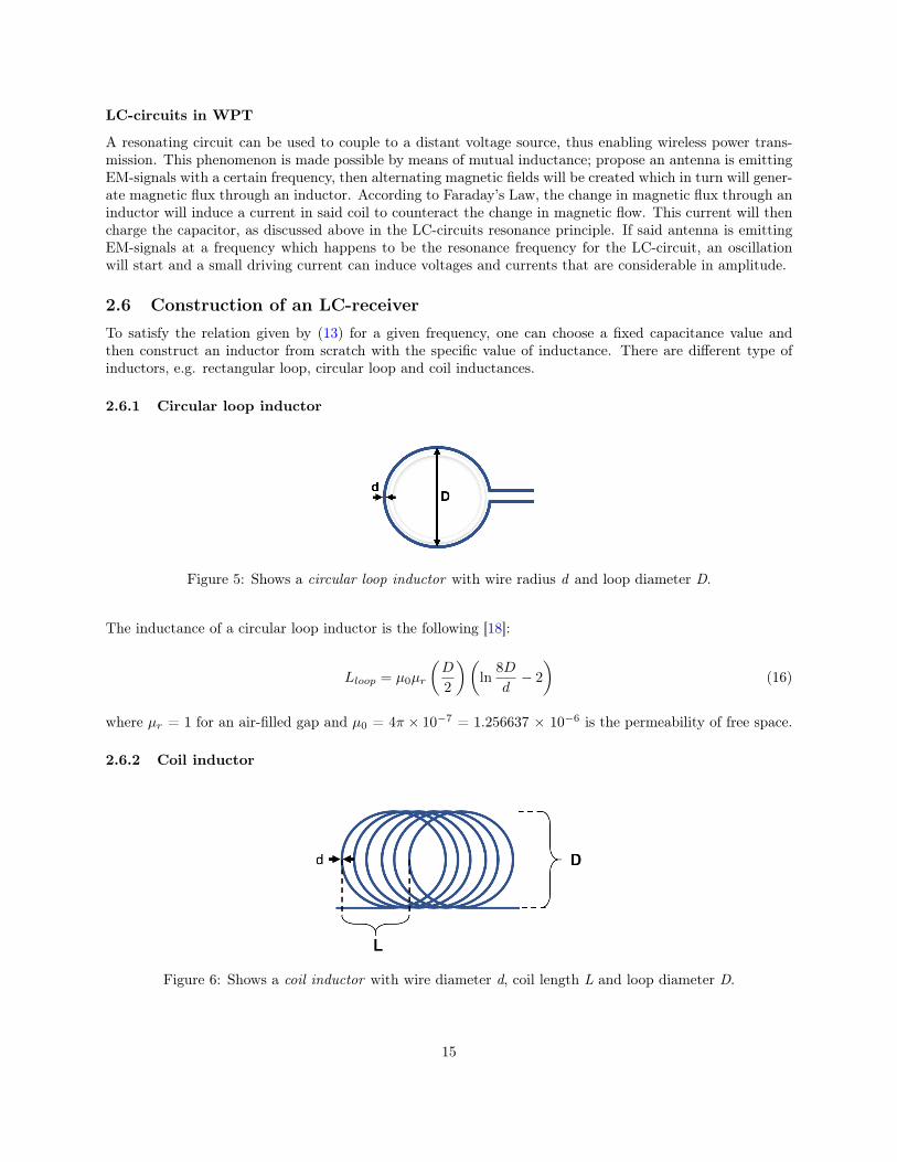
Figure 5: Shows a circular loop inductor with wire radius d and loop diameter D.
The inductance of a circular loop inductor is the following [18]:
Lloop = µ0µr
(D
2
)(ln
8D
d− 2
)(16)
where µr = 1 for an air-filled gap and µ0 = 4π × 10−7 = 1.256637 × 10⁻⁶ is the permeability of free space.
2.6.2 Coil inductor
Figure 6: Shows a coil inductor with wire diameter d, coil length L and loop diameter D.
15
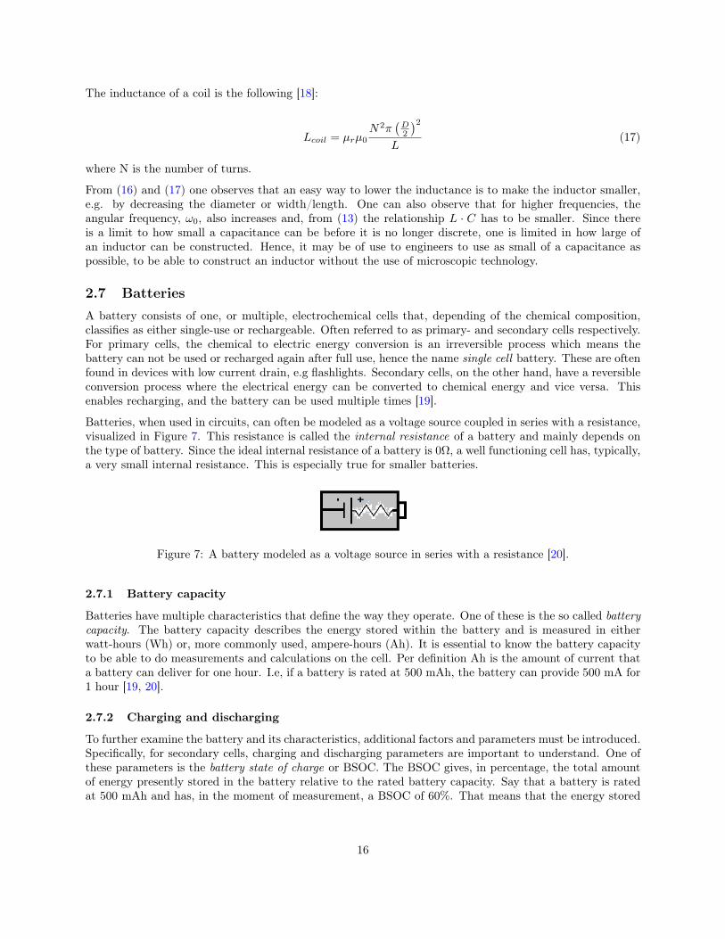
The inductance of a coil is the following [18]:
Lcoil = µrµ0
N2π(D2
)2L
(17)
where N is the number of turns.
From (16) and (17) one observes that an easy way to lower the inductance is to make the inductor smaller,e.g. by decreasing the diameter or width/length. One can also observe that for higher frequencies, theangular frequency, ω0, also increases and, from (13) the relationship L · C has to be smaller. Since thereis a limit to how small a capacitance can be before it is no longer discrete, one is limited in how large ofan inductor can be constructed. Hence, it may be of use to engineers to use as small of a capacitance aspossible, to be able to construct an inductor without the use of microscopic technology.
2.7 BatteriesA battery consists of one, or multiple, electrochemical cells that, depending of the chemical composition,classifies as either single-use or rechargeable. Often referred to as primary- and secondary cells respectively.For primary cells, the chemical to electric energy conversion is an irreversible process which means thebattery can not be used or recharged again after full use, hence the name single cell battery. These are oftenfound in devices with low current drain, e.g flashlights. Secondary cells, on the other hand, have a reversibleconversion process where the electrical energy can be converted to chemical energy and vice versa. Thisenables recharging, and the battery can be used multiple times [19].
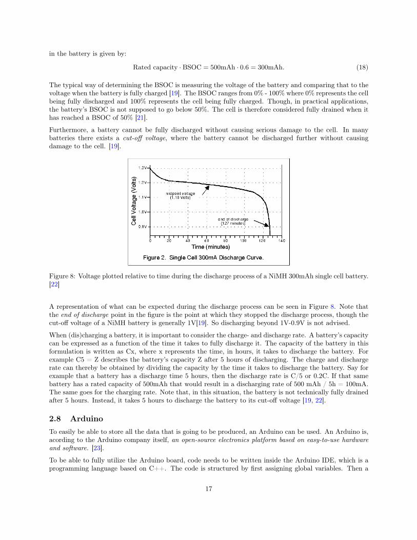
Batteries, when used in circuits, can often be modeled as a voltage source coupled in series with a resistance,visualized in Figure 7. This resistance is called the internal resistance of a battery and mainly depends onthe type of battery. Since the ideal internal resistance of a battery is 0Ω, a well functioning cell has, typically,a very small internal resistance. This is especially true for smaller batteries.
Figure 7: A battery modeled as a voltage source in series with a resistance [20].
2.7.1 Battery capacity
Batteries have multiple characteristics that define the way they operate. One of these is the so called batterycapacity. The battery capacity describes the energy stored within the battery and is measured in eitherwatt-hours (Wh) or, more commonly used, ampere-hours (Ah). It is essential to know the battery capacityto be able to do measurements and calculations on the cell. Per definition Ah is the amount of current thata battery can deliver for one hour. I.e, if a battery is rated at 500 mAh, the battery can provide 500 mA for1 hour [19, 20].
2.7.2 Charging and discharging
To further examine the battery and its characteristics, additional factors and parameters must be introduced.Specifically, for secondary cells, charging and discharging parameters are important to understand. One ofthese parameters is the battery state of charge or BSOC. The BSOC gives, in percentage, the total amountof energy presently stored in the battery relative to the rated battery capacity. Say that a battery is ratedat 500 mAh and has, in the moment of measurement, a BSOC of 60%. That means that the energy stored
16
in the battery is given by:
Rated capacity · BSOC = 500mAh · 0.6 = 300mAh. (18)
The typical way of determining the BSOC is measuring the voltage of the battery and comparing that to thevoltage when the battery is fully charged [19]. The BSOC ranges from 0% - 100% where 0% represents the cellbeing fully discharged and 100% represents the cell being fully charged. Though, in practical applications,the battery’s BSOC is not supposed to go below 50%. The cell is therefore considered fully drained when ithas reached a BSOC of 50% [21].
Furthermore, a battery cannot be fully discharged without causing serious damage to the cell. In manybatteries there exists a cut-off voltage, where the battery cannot be discharged further without causingdamage to the cell. [19].
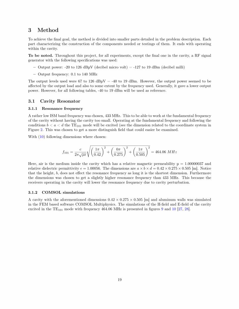
Figure 8: Voltage plotted relative to time during the discharge process of a NiMH 300mAh single cell battery.[22]
A representation of what can be expected during the discharge process can be seen in Figure 8. Note thatthe end of discharge point in the figure is the point at which they stopped the discharge process, though thecut-off voltage of a NiMH battery is generally 1V[19]. So discharging beyond 1V-0.9V is not advised.
When (dis)charging a battery, it is important to consider the charge- and discharge rate. A battery’s capacitycan be expressed as a function of the time it takes to fully discharge it. The capacity of the battery in thisformulation is written as Cx, where x represents the time, in hours, it takes to discharge the battery. Forexample C5 = Z describes the battery’s capacity Z after 5 hours of discharging. The charge and dischargerate can thereby be obtained by dividing the capacity by the time it takes to discharge the battery. Say forexample that a battery has a discharge time 5 hours, then the discharge rate is C/5 or 0.2C. If that samebattery has a rated capacity of 500mAh that would result in a discharging rate of 500 mAh / 5h = 100mA.The same goes for the charging rate. Note that, in this situation, the battery is not technically fully drainedafter 5 hours. Instead, it takes 5 hours to discharge the battery to its cut-off voltage [19, 22].
2.8 ArduinoTo easily be able to store all the data that is going to be produced, an Arduino can be used. An Arduino is,acording to the Arduino company itself, an open-source electronics platform based on easy-to-use hardwareand software. [23].
To be able to fully utilize the Arduino board, code needs to be written inside the Arduino IDE, which is aprogramming language based on C++. The code is structured by first assigning global variables. Then a
17

void setup(), i.e. a function that will only run once, where input pin modes etc. is initialized. Other void ...()-functions can also be specified. Afterwards, a void loop() can be added, which will loop the commandsinside the bracket. Here, the void functions can be called. Further, by the command Serial.print, wantedvalues can be printed in the Serial monitor. [24].
Reading a voltage with an Arduino connected to an analog sensor pin, will by the analog-to-digital converter(ADC), converts it into a number between 0 and 1023. Thus the input voltage can be calculated by[25]:
Voltage = sensorValue · Ref. voltage1023
. (19)
The reference voltage is normally 5V, but sometimes it has to be calibrated as some Arduino boards havedifferent reference voltages. Furthermore, the reference voltage can also be lowered with a load to the 5Voutput pin. Especially if the Arduino is powered by a USB connection with 5V instead of a external powersupply of higher voltage (6-12V) to the VIN pin.
2.9 Vector Network AnalyzerA vector network analyzer (VNA) is a type of electronic test instrument used in high frequency applications.The device measures transmitted and reflected waves and compares it to the input signal [26]. The inputsignal has a wide frequency range, which can also be used to excite a cavity. The VNA can also used todecide a cavity’s or an LC-circuit’s resonance frequency. This is valuable since it can be used to compareresults to theoretical findings.
18
3 MethodTo achieve the final goal, the method is divided into smaller parts detailed in the problem description. Eachpart characterizing the construction of the components needed or testings of them. It ends with operatingwithin the cavity.
To be noted. Throughout this project, for all experiments, except the final one in the cavity, a RF signalgenerator with the following specifications was used:
− Output power: -20 to 126 dBµV (decibel micro volt) = -127 to 19 dBm (decibel milli)
− Output frequency: 0.1 to 140 MHz
The output levels used were 67 to 126 dBµV = -40 to 19 dBm. However, the output power seemed to beaffected by the output load and also to some extent by the frequency used. Generally, it gave a lower outputpower. However, for all following tables, -40 to 19 dBm will be used as reference.
3.1 Cavity Resonator3.1.1 Resonance frequency
A rather low ISM band frequency was chosen, 433 MHz. This to be able to work at the fundamental frequencyof the cavity without having the cavity too small. Operating at the fundamental frequency and following theconditions b < a < d the TE101 mode will be excited (see the dimension related to the coordinate system inFigure 2. This was chosen to get a more distinguish field that could easier be examined.
With (10) following dimensions where chosen:
f101 =c
2π√µε
√(1π
0.42
)2
+
(0π
0.275
)2
+
(1π
0.505
)2
= 464.06 MHz
Here, air is the medium inside the cavity which has a relative magnetic permeability µ = 1.00000037 andrelative dielectric permittivity ε = 1.00056. The dimensions are a× b× d = 0.42× 0.275× 0.505 [m]. Noticethat the height, b, does not effect the resonance frequency as long it is the shortest dimension. Furthermorethe dimensions was chosen to get a slightly higher resonance frequency than 433 MHz. This because thereceivers operating in the cavity will lower the resonance frequency due to cavity perturbation.
3.1.2 COMSOL simulations
A cavity with the aforementioned dimensions 0.42 × 0.275 × 0.505 [m] and aluminum walls was simulatedin the FEM based software COMSOL Multiphysics. The simulations of the H-field and E-field of the cavityexcited in the TE101 mode with frequency 464.06 MHz is presented in figures 9 and 10 [27, 28].
19
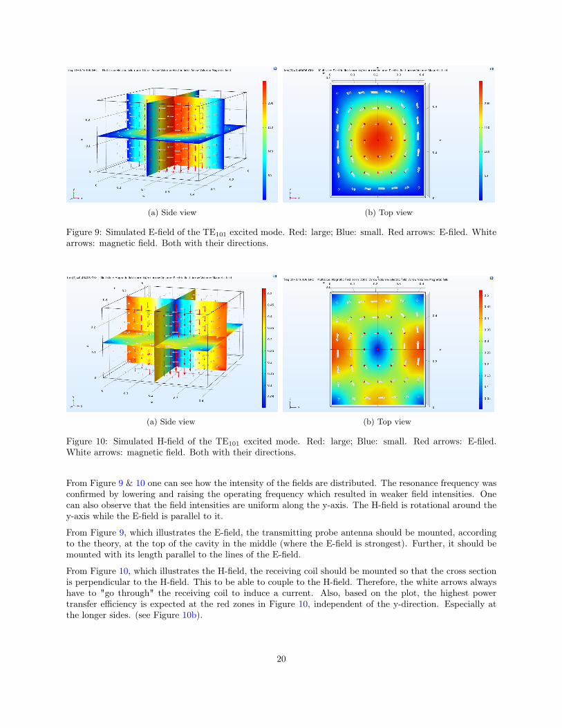
(a) Side view (b) Top view
Figure 9: Simulated E-field of the TE101 excited mode. Red: large; Blue: small. Red arrows: E-filed. Whitearrows: magnetic field. Both with their directions.
(a) Side view (b) Top view
Figure 10: Simulated H-field of the TE101 excited mode. Red: large; Blue: small. Red arrows: E-filed.White arrows: magnetic field. Both with their directions.
From Figure 9 & 10 one can see how the intensity of the fields are distributed. The resonance frequency wasconfirmed by lowering and raising the operating frequency which resulted in weaker field intensities. Onecan also observe that the field intensities are uniform along the y-axis. The H-field is rotational around they-axis while the E-field is parallel to it.
From Figure 9, which illustrates the E-field, the transmitting probe antenna should be mounted, accordingto the theory, at the top of the cavity in the middle (where the E-field is strongest). Further, it should bemounted with its length parallel to the lines of the E-field.
From Figure 10, which illustrates the H-field, the receiving coil should be mounted so that the cross sectionis perpendicular to the H-field. This to be able to couple to the H-field. Therefore, the white arrows alwayshave to "go through" the receiving coil to induce a current. Also, based on the plot, the highest powertransfer efficiency is expected at the red zones in Figure 10, independent of the y-direction. Especially atthe longer sides. (see Figure 10b).
20
3.1.3 Construction of the cavity
A cavity resonator was built using:
− Aluminum foil
− Aluminum tape
− Cardboard
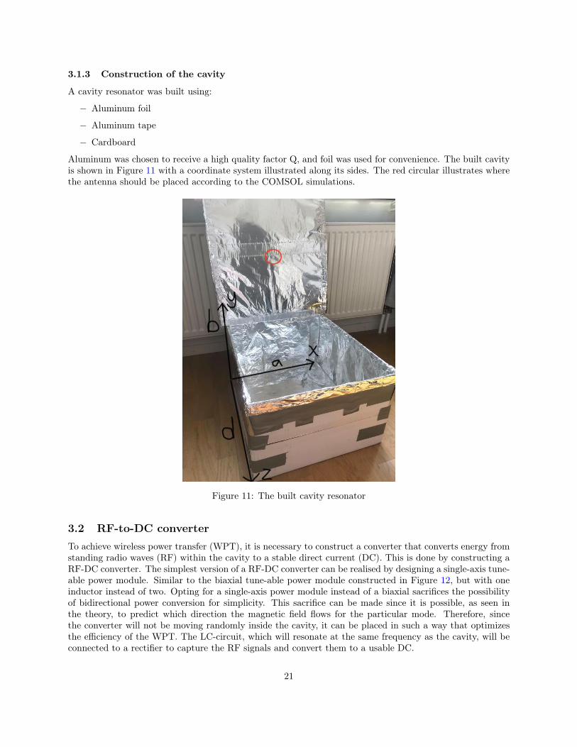
Aluminum was chosen to receive a high quality factor Q, and foil was used for convenience. The built cavityis shown in Figure 11 with a coordinate system illustrated along its sides. The red circular illustrates wherethe antenna should be placed according to the COMSOL simulations.
Figure 11: The built cavity resonator
3.2 RF-to-DC converterTo achieve wireless power transfer (WPT), it is necessary to construct a converter that converts energy fromstanding radio waves (RF) within the cavity to a stable direct current (DC). This is done by constructing aRF-DC converter. The simplest version of a RF-DC converter can be realised by designing a single-axis tune-able power module. Similar to the biaxial tune-able power module constructed in Figure 12, but with oneinductor instead of two. Opting for a single-axis power module instead of a biaxial sacrifices the possibilityof bidirectional power conversion for simplicity. This sacrifice can be made since it is possible, as seen inthe theory, to predict which direction the magnetic field flows for the particular mode. Therefore, sincethe converter will not be moving randomly inside the cavity, it can be placed in such a way that optimizesthe efficiency of the WPT. The LC-circuit, which will resonate at the same frequency as the cavity, will beconnected to a rectifier to capture the RF signals and convert them to a usable DC.
21
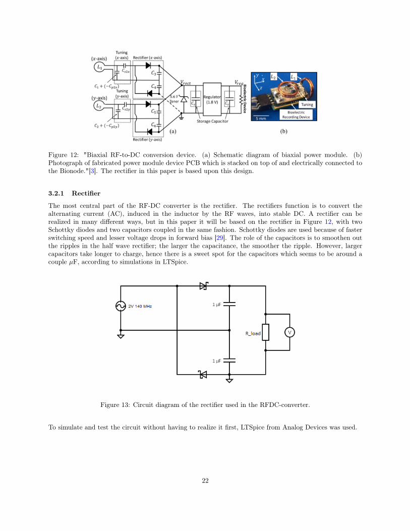
Figure 12: "Biaxial RF-to-DC conversion device. (a) Schematic diagram of biaxial power module. (b)Photograph of fabricated power module device PCB which is stacked on top of and electrically connected tothe Bionode."[3]. The rectifier in this paper is based upon this design.
3.2.1 Rectifier
The most central part of the RF-DC converter is the rectifier. The rectifiers function is to convert thealternating current (AC), induced in the inductor by the RF waves, into stable DC. A rectifier can berealized in many different ways, but in this paper it will be based on the rectifier in Figure 12, with twoSchottky diodes and two capacitors coupled in the same fashion. Schottky diodes are used because of fasterswitching speed and lesser voltage drops in forward bias [29]. The role of the capacitors is to smoothen outthe ripples in the half wave rectifier; the larger the capacitance, the smoother the ripple. However, largercapacitors take longer to charge, hence there is a sweet spot for the capacitors which seems to be around acouple µF, according to simulations in LTSpice.
Figure 13: Circuit diagram of the rectifier used in the RFDC-converter.
To simulate and test the circuit without having to realize it first, LTSpice from Analog Devices was used.
22
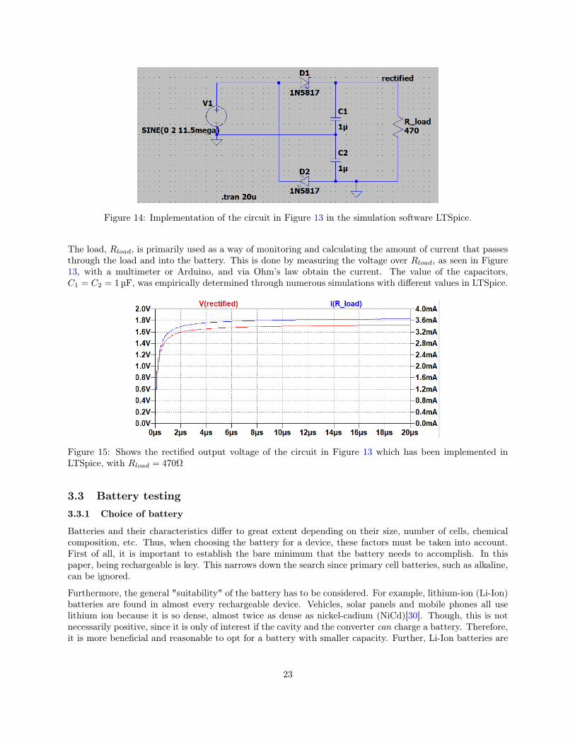
Figure 14: Implementation of the circuit in Figure 13 in the simulation software LTSpice.
The load, Rload, is primarily used as a way of monitoring and calculating the amount of current that passesthrough the load and into the battery. This is done by measuring the voltage over Rload, as seen in Figure13, with a multimeter or Arduino, and via Ohm’s law obtain the current. The value of the capacitors,C1 = C2 = 1 µF, was empirically determined through numerous simulations with different values in LTSpice.
Figure 15: Shows the rectified output voltage of the circuit in Figure 13 which has been implemented inLTSpice, with Rload = 470Ω
3.3 Battery testing3.3.1 Choice of battery
Batteries and their characteristics differ to great extent depending on their size, number of cells, chemicalcomposition, etc. Thus, when choosing the battery for a device, these factors must be taken into account.First of all, it is important to establish the bare minimum that the battery needs to accomplish. In thispaper, being rechargeable is key. This narrows down the search since primary cell batteries, such as alkaline,can be ignored.
Furthermore, the general "suitability" of the battery has to be considered. For example, lithium-ion (Li-Ion)batteries are found in almost every rechargeable device. Vehicles, solar panels and mobile phones all uselithium ion because it is so dense, almost twice as dense as nickel-cadium (NiCd)[30]. Though, this is notnecessarily positive, since it is only of interest if the cavity and the converter can charge a battery. Therefore,it is more beneficial and reasonable to opt for a battery with smaller capacity. Further, Li-Ion batteries are
23
generally quite unsafe. Especially in a relatively uncontrolled environment[31], which applies here. Thus,Li-Ion batteries are not applicable here.
The aforementioned NiCd battery is another option. The NiCd is a rigid type of battery that handlesuncontrolled charging and discharging very well. It used to be a very popular battery when it came torechargeable cells, and was available in various shapes and sizes[31]. It would have been a great option, butit is outdated and does not exists on the market, at least not as AAA-battery. AAA seemed to be the bestchoice since it is small, has generally low rated voltage, is easily accessible and generally allows recharging.Though, a battery inside a small drone would have to be way smaller than an AAA-battery.
The NiCd’s lack of market real estate mostly comes from the invention of the Nickel-Metal Hydride (NiMH)battery, and due to NiMH being more environmentally friendly. Though, there are some setbacks when optingfor the NiMH instead of the NiCd. For example, the NiMH is not quite as rigid as NiCd and requires a moreparticular charging and discharging range. A discharge current of between 0.2C to 0.5C is recommended. Italso requires a more complex charging regime. Since it generates more heat during charging it needs longercharging times. Lower charging rates is also an option, but needs to be done with care, since there is a riskof overcharging and damaging the NiMH cell [31].
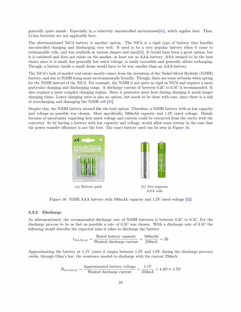
Despite this, the NiMH battery seemed like the best option. Therefore, a NiMH battery with as low capacityand voltage as possible was chosen. More specifically, 500mAh capacity and 1.2V rated voltage. Mainlybecause of uncertainty regarding how much voltage and current could be extracted from the cavity with theconverter. So by having a battery with low capacity and voltage, would allow some leeway in the case thatthe power transfer efficiency is not the best. The exact battery used can be seen in Figure 16.
(a) Battery pack (b) Two separateAAA cells
Figure 16: NiMH AAA battery with 500mAh capacity and 1.2V rated voltage [32]
3.3.2 Discharge
As aforementioned, the recommended discharge rate of NiMH batteries is between 0.2C to 0.5C. For thedischarge process to be as fast as possible a rate of 0.5C was chosen. With a discharge rate of 0.5C thefollowing would describe the expected time it takes to discharge the battery:
tdischarge =Rated battery capacity
Wanted discharge current=
500mAh250mA
= 2h
Approximating the battery at 1.1V (since it ranges between 1.2V and 1.0V during the discharge process)yields, through Ohm’s law, the resistance needed to discharge with the current 250mA:
Rdischarge =Approximated battery voltage
Wanted discharge current=
1.1V250mA
= 4.4Ω ≈ 4.7Ω
24
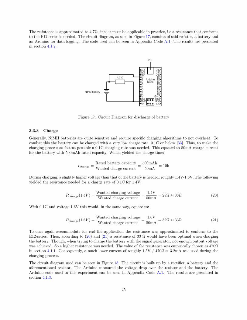
The resistance is approximated to 4.7Ω since it must be applicable in practice, i.e a resistance that conformsto the E12-series is needed. The circuit diagram, as seen in Figure 17, consists of said resistor, a battery andan Arduino for data logging. The code used can be seen in Appendix Code A.1. The results are presentedin section 4.1.2.
Figure 17: Circuit Diagram for discharge of battery
3.3.3 Charge
Generally, NiMH batteries are quite sensitive and require specific charging algorithms to not overheat. Tocombat this the battery can be charged with a very low charge rate, 0.1C or below [33]. Thus, to make thecharging process as fast as possible a 0.1C charging rate was needed. This equated to 50mA charge currentfor the battery with 500mAh rated capacity. Which yielded the charge time:
tcharge =Rated battery capacityWanted charge current
=500mAh50mA
= 10h
During charging, a slightly higher voltage than that of the battery is needed, roughly 1.4V-1.6V. The followingyielded the resistance needed for a charge rate of 0.1C for 1.4V:
Rcharge(1.4V ) =Wanted charging voltageWanted charge current
=1.4V50mA
= 28Ω ≈ 33Ω (20)
With 0.1C and voltage 1.6V this would, in the same way, equate to:
Rcharge(1.6V ) =Wanted charging voltageWanted charge current
=1.6V50mA
= 32Ω ≈ 33Ω (21)
To once again accommodate for real life application the resistance was approximated to conform to theE12-series. Thus, according to (20) and (21) a resistance of 33 Ω would have been optimal when chargingthe battery. Though, when trying to charge the battery with the signal generator, not enough output voltagewas achieved. So a higher resistance was needed. The value of the resistance was empirically chosen as 470Ωin section 4.1.1. Consequently, a much lower current of roughly 1.5V / 470Ω ≈ 3.2mA was used during thecharging process.
The circuit diagram used can be seen in Figure 18. The circuit is built up by a rectifier, a battery and theaforementioned resistor. The Arduino measured the voltage drop over the resistor and the battery. TheArduino code used in this experiment can be seen in Appendix Code A.1. The results are presented insection 4.1.3.
25
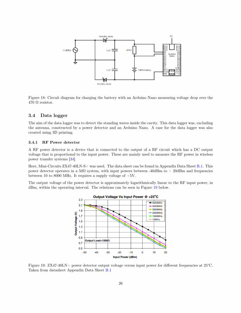
Figure 18: Circuit diagram for charging the battery with an Arduino Nano measuring voltage drop over the470 Ω resistor.
3.4 Data loggerThe aim of the data logger was to detect the standing waves inside the cavity. This data logger was, excludingthe antenna, constructed by a power detector and an Arduino Nano. A case for the data logger was alsocreated using 3D printing.
3.4.1 RF Power detector
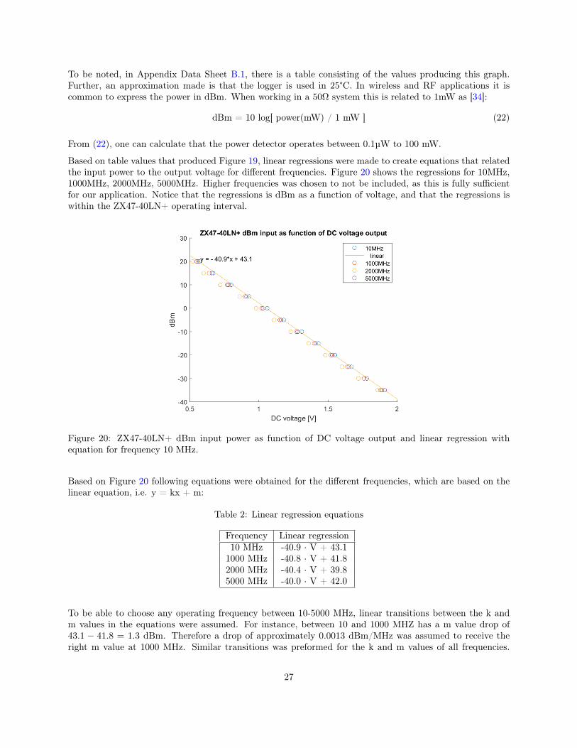
A RF power detector is a device that is connected to the output of a RF circuit which has a DC outputvoltage that is proportional to the input power. These are mainly used to measure the RF power in wirelesspower transfer systems [34].
Here, Mini-Circuits ZX47-40LN-S+ was used. The data sheet can be found in Appendix Data Sheet B.1. Thispower detector operates in a 50Ω system, with input powers between -40dBm to + 20dBm and frequenciesbetween 10 to 8000 MHz. It requires a supply voltage of +5V.
The output voltage of the power detector is approximately logarithmically linear to the RF input power, indBm, within the operating interval. The relations can be seen in Figure 19 below.
Figure 19: ZX47-40LN+ power detector output voltage versus input power for different frequencies at 25°C.Taken from datasheet Appendix Data Sheet B.1
26
To be noted, in Appendix Data Sheet B.1, there is a table consisting of the values producing this graph.Further, an approximation made is that the logger is used in 25°C. In wireless and RF applications it iscommon to express the power in dBm. When working in a 50Ω system this is related to 1mW as [34]:
dBm = 10 log[ power(mW) / 1 mW ] (22)
From (22), one can calculate that the power detector operates between 0.1µW to 100 mW.
Based on table values that produced Figure 19, linear regressions were made to create equations that relatedthe input power to the output voltage for different frequencies. Figure 20 shows the regressions for 10MHz,1000MHz, 2000MHz, 5000MHz. Higher frequencies was chosen to not be included, as this is fully sufficientfor our application. Notice that the regressions is dBm as a function of voltage, and that the regressions iswithin the ZX47-40LN+ operating interval.
Figure 20: ZX47-40LN+ dBm input power as function of DC voltage output and linear regression withequation for frequency 10 MHz.
Based on Figure 20 following equations were obtained for the different frequencies, which are based on thelinear equation, i.e. y = kx + m:
Table 2: Linear regression equations
Frequency Linear regression10 MHz -40.9 · V + 43.11000 MHz -40.8 · V + 41.82000 MHz -40.4 · V + 39.85000 MHz -40.0 · V + 42.0
To be able to choose any operating frequency between 10-5000 MHz, linear transitions between the k andm values in the equations were assumed. For instance, between 10 and 1000 MHZ has a m value drop of43.1 − 41.8 = 1.3 dBm. Therefore a drop of approximately 0.0013 dBm/MHz was assumed to receive theright m value at 1000 MHz. Similar transitions was preformed for the k and m values of all frequencies.
27
This was implemented in the Arduino code. The code asks the user to chose an arbitrary frequency between10-5000 MHz.
Furthermore, since the input to the Arduinos sensor pin probably will have some variation, the code wasstructured as follows [35]:
− Takes a sample every 10 ms.
− Store these values and calculate the average over 2 s.
3.4.2 Construction and testing
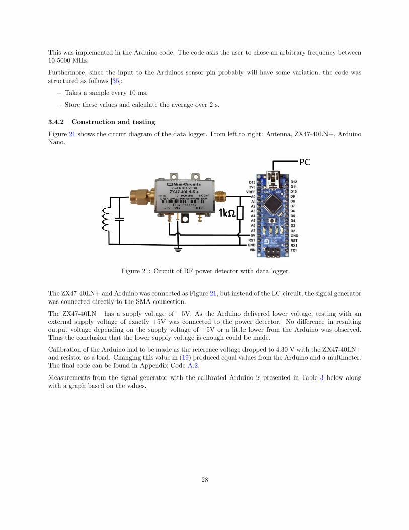
Figure 21 shows the circuit diagram of the data logger. From left to right: Antenna, ZX47-40LN+, ArduinoNano.
Figure 21: Circuit of RF power detector with data logger
The ZX47-40LN+ and Arduino was connected as Figure 21, but instead of the LC-circuit, the signal generatorwas connected directly to the SMA connection.
The ZX47-40LN+ has a supply voltage of +5V. As the Arduino delivered lower voltage, testing with anexternal supply voltage of exactly +5V was connected to the power detector. No difference in resultingoutput voltage depending on the supply voltage of +5V or a little lower from the Arduino was observed.Thus the conclusion that the lower supply voltage is enough could be made.
Calibration of the Arduino had to be made as the reference voltage dropped to 4.30 V with the ZX47-40LN+and resistor as a load. Changing this value in (19) produced equal values from the Arduino and a multimeter.The final code can be found in Appendix Code A.2.
Measurements from the signal generator with the calibrated Arduino is presented in Table 3 below alongwith a graph based on the values.
28
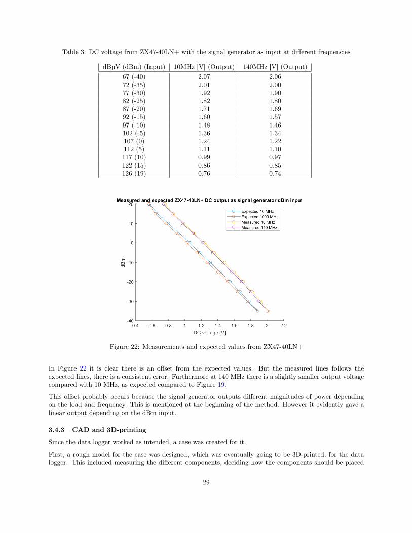
Table 3: DC voltage from ZX47-40LN+ with the signal generator as input at different frequencies
dBµV (dBm) (Input) 10MHz [V] (Output) 140MHz [V] (Output)67 (-40) 2.07 2.0672 (-35) 2.01 2.0077 (-30) 1.92 1.9082 (-25) 1.82 1.8087 (-20) 1.71 1.6992 (-15) 1.60 1.5797 (-10) 1.48 1.46102 (-5) 1.36 1.34107 (0) 1.24 1.22112 (5) 1.11 1.10117 (10) 0.99 0.97122 (15) 0.86 0.85126 (19) 0.76 0.74
Figure 22: Measurements and expected values from ZX47-40LN+
In Figure 22 it is clear there is an offset from the expected values. But the measured lines follows theexpected lines, there is a consistent error. Furthermore at 140 MHz there is a slightly smaller output voltagecompared with 10 MHz, as expected compared to Figure 19.
This offset probably occurs because the signal generator outputs different magnitudes of power dependingon the load and frequency. This is mentioned at the beginning of the method. However it evidently gave alinear output depending on the dBm input.
3.4.3 CAD and 3D-printing
Since the data logger worked as intended, a case was created for it.
First, a rough model for the case was designed, which was eventually going to be 3D-printed, for the datalogger. This included measuring the different components, deciding how the components should be placed
29
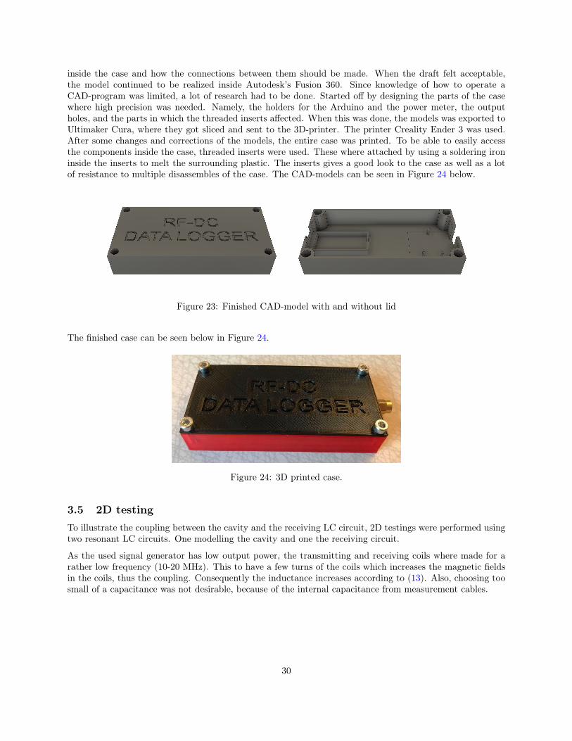
inside the case and how the connections between them should be made. When the draft felt acceptable,the model continued to be realized inside Autodesk’s Fusion 360. Since knowledge of how to operate aCAD-program was limited, a lot of research had to be done. Started off by designing the parts of the casewhere high precision was needed. Namely, the holders for the Arduino and the power meter, the outputholes, and the parts in which the threaded inserts affected. When this was done, the models was exported toUltimaker Cura, where they got sliced and sent to the 3D-printer. The printer Creality Ender 3 was used.After some changes and corrections of the models, the entire case was printed. To be able to easily accessthe components inside the case, threaded inserts were used. These where attached by using a soldering ironinside the inserts to melt the surrounding plastic. The inserts gives a good look to the case as well as a lotof resistance to multiple disassembles of the case. The CAD-models can be seen in Figure 24 below.
Figure 23: Finished CAD-model with and without lid
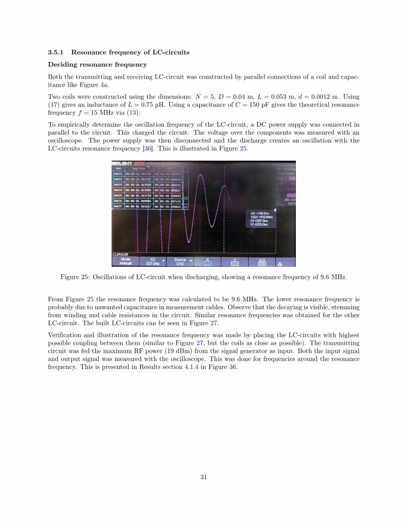
The finished case can be seen below in Figure 24.
Figure 24: 3D printed case.
3.5 2D testingTo illustrate the coupling between the cavity and the receiving LC circuit, 2D testings were performed usingtwo resonant LC circuits. One modelling the cavity and one the receiving circuit.
As the used signal generator has low output power, the transmitting and receiving coils where made for arather low frequency (10-20 MHz). This to have a few turns of the coils which increases the magnetic fieldsin the coils, thus the coupling. Consequently the inductance increases according to (13). Also, choosing toosmall of a capacitance was not desirable, because of the internal capacitance from measurement cables.
30
3.5.1 Resonance frequency of LC-circuits
Deciding resonance frequency
Both the transmitting and receiving LC-circuit was constructed by parallel connections of a coil and capac-itance like Figure 4a.
Two coils were constructed using the dimensions: N = 5, D = 0.04 m, L = 0.053 m, d = 0.0012 m. Using(17) gives an inductance of L = 0.75 µH. Using a capacitance of C = 150 pF gives the theoretical resonancefrequency f = 15 MHz via (13).
To empirically determine the oscillation frequency of the LC-circuit, a DC power supply was connected inparallel to the circuit. This charged the circuit. The voltage over the components was measured with anoscilloscope. The power supply was then disconnected and the discharge creates an oscillation with theLC-circuits resonance frequency [36]. This is illustrated in Figure 25.
Figure 25: Oscillations of LC-circuit when discharging, showing a resonance frequency of 9.6 MHz.
From Figure 25 the resonance frequency was calculated to be 9.6 MHz. The lower resonance frequency isprobably due to unwanted capacitance in measurement cables. Observe that the decaying is visible, stemmingfrom winding and cable resistances in the circuit. Similar resonance frequencies was obtained for the otherLC-circuit. The built LC-circuits can be seen in Figure 27.
Verification and illustration of the resonance frequency was made by placing the LC-circuits with highestpossible coupling between them (similar to Figure 27, but the coils as close as possible). The transmittingcircuit was fed the maximum RF power (19 dBm) from the signal generator as input. Both the input signaland output signal was measured with the oscilloscope. This was done for frequencies around the resonancefrequency. This is presented in Results section 4.1.4 in Figure 36.
31
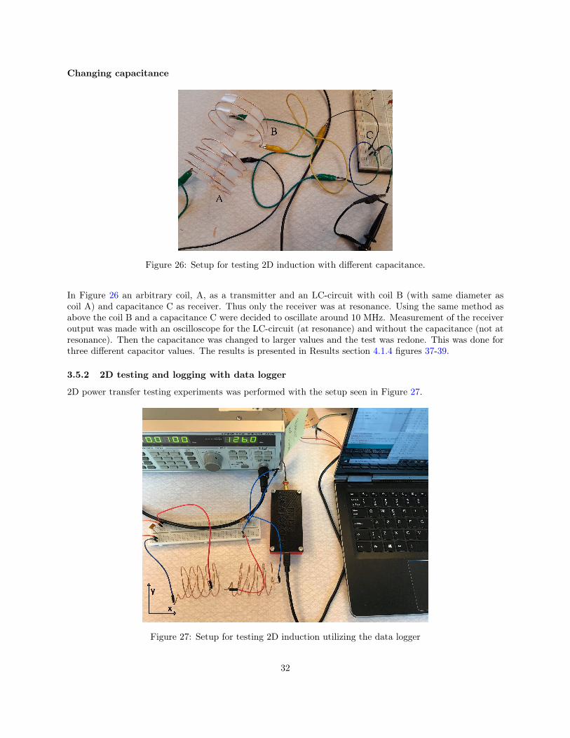
Changing capacitance
Figure 26: Setup for testing 2D induction with different capacitance.
In Figure 26 an arbitrary coil, A, as a transmitter and an LC-circuit with coil B (with same diameter ascoil A) and capacitance C as receiver. Thus only the receiver was at resonance. Using the same method asabove the coil B and a capacitance C were decided to oscillate around 10 MHz. Measurement of the receiveroutput was made with an oscilloscope for the LC-circuit (at resonance) and without the capacitance (not atresonance). Then the capacitance was changed to larger values and the test was redone. This was done forthree different capacitor values. The results is presented in Results section 4.1.4 figures 37-39.
3.5.2 2D testing and logging with data logger
2D power transfer testing experiments was performed with the setup seen in Figure 27.
Figure 27: Setup for testing 2D induction utilizing the data logger
32
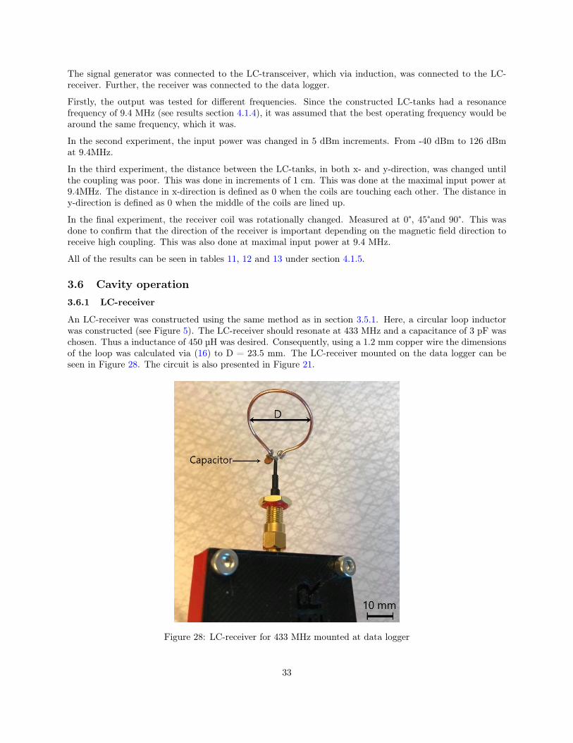
The signal generator was connected to the LC-transceiver, which via induction, was connected to the LC-receiver. Further, the receiver was connected to the data logger.
Firstly, the output was tested for different frequencies. Since the constructed LC-tanks had a resonancefrequency of 9.4 MHz (see results section 4.1.4), it was assumed that the best operating frequency would bearound the same frequency, which it was.
In the second experiment, the input power was changed in 5 dBm increments. From -40 dBm to 126 dBmat 9.4MHz.
In the third experiment, the distance between the LC-tanks, in both x- and y-direction, was changed untilthe coupling was poor. This was done in increments of 1 cm. This was done at the maximal input power at9.4MHz. The distance in x-direction is defined as 0 when the coils are touching each other. The distance iny-direction is defined as 0 when the middle of the coils are lined up.
In the final experiment, the receiver coil was rotationally changed. Measured at 0°, 45°and 90°. This wasdone to confirm that the direction of the receiver is important depending on the magnetic field direction toreceive high coupling. This was also done at maximal input power at 9.4 MHz.
All of the results can be seen in tables 11, 12 and 13 under section 4.1.5.
3.6 Cavity operation3.6.1 LC-receiver
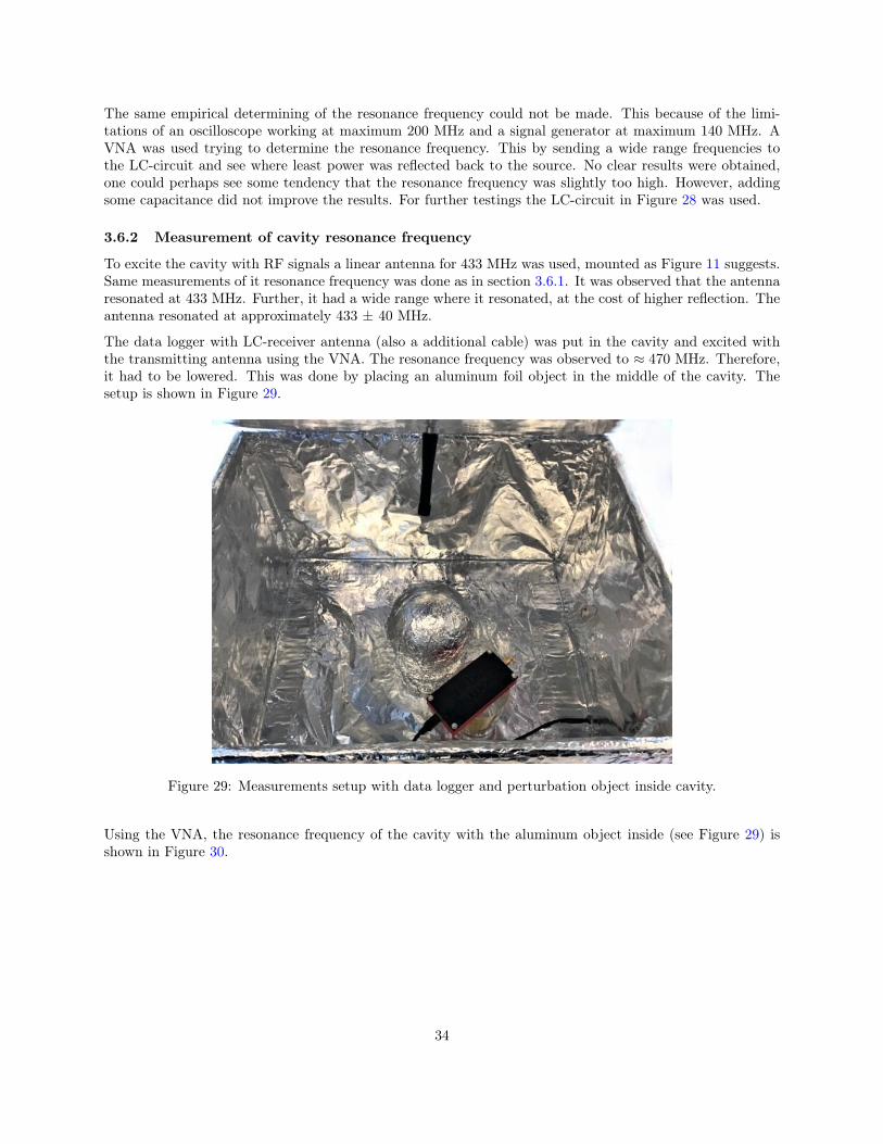
An LC-receiver was constructed using the same method as in section 3.5.1. Here, a circular loop inductorwas constructed (see Figure 5). The LC-receiver should resonate at 433 MHz and a capacitance of 3 pF waschosen. Thus a inductance of 450 µH was desired. Consequently, using a 1.2 mm copper wire the dimensionsof the loop was calculated via (16) to D = 23.5 mm. The LC-receiver mounted on the data logger can beseen in Figure 28. The circuit is also presented in Figure 21.
Figure 28: LC-receiver for 433 MHz mounted at data logger
33
The same empirical determining of the resonance frequency could not be made. This because of the limi-tations of an oscilloscope working at maximum 200 MHz and a signal generator at maximum 140 MHz. AVNA was used trying to determine the resonance frequency. This by sending a wide range frequencies tothe LC-circuit and see where least power was reflected back to the source. No clear results were obtained,one could perhaps see some tendency that the resonance frequency was slightly too high. However, addingsome capacitance did not improve the results. For further testings the LC-circuit in Figure 28 was used.
3.6.2 Measurement of cavity resonance frequency
To excite the cavity with RF signals a linear antenna for 433 MHz was used, mounted as Figure 11 suggests.Same measurements of it resonance frequency was done as in section 3.6.1. It was observed that the antennaresonated at 433 MHz. Further, it had a wide range where it resonated, at the cost of higher reflection. Theantenna resonated at approximately 433 ± 40 MHz.
The data logger with LC-receiver antenna (also a additional cable) was put in the cavity and excited withthe transmitting antenna using the VNA. The resonance frequency was observed to ≈ 470 MHz. Therefore,it had to be lowered. This was done by placing an aluminum foil object in the middle of the cavity. Thesetup is shown in Figure 29.
Figure 29: Measurements setup with data logger and perturbation object inside cavity.
Using the VNA, the resonance frequency of the cavity with the aluminum object inside (see Figure 29) isshown in Figure 30.
34
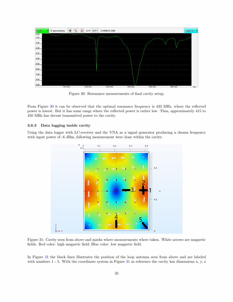
Figure 30: Resonance measurements of final cavity setup.
From Figure 30 it can be observed that the optimal resonance frequency is 433 MHz, where the reflectedpower is lowest. But it has some range where the reflected power is rather low. Thus, approximately 415 to450 MHz has decent transmitted power to the cavity.
3.6.3 Data logging inside cavity
Using the data logger with LC-receiver and the VNA as a signal generator producing a chosen frequencywith input power of -6 dBm, following measurement were done within the cavity:
Figure 31: Cavity seen from above and marks where measurements where taken. White arrows are magneticfields. Red color: high magnetic field; Blue color: low magnetic field.
In Figure 31 the black lines illustrates the position of the loop antenna seen from above and are labeledwith numbers 1 - 5. With the coordinate system in Figure 31 as reference the cavity has dimensions x, y, z
35

= 0.42 x 0.275 x 0.505 [m]. All measurements were performed at half the cavity height i.e. y = 0.1375 m.Additionally all measurements except measurement no. 2 where performed at the lowest possible height y =0.015m. These had the same x, z positions and will be labeled 1.1 - 5.1. All measurement where performedat 433 MHz.
At locations 1 and 1.1 measurements were also performed at lower and higher frequencies.
Fractions of the received power relative the transmitted power from the VNA i.e. the power transfer efficiency(PTE) was calculated.
All results can be seen in Results section 4.2.
36
4 Results and discussion
4.1 Primary testings4.1.1 RF-DC converter
Table 4-10 shows the frequency f [MHz] generated by the signal generator, average voltage0 V [mV] andripples peak-to-peak (p2p) [mV] read from the oscilloscope over different resistors plugged into the rectifierin Figure 18.
Table 4: 33Ω
f [MHz] V [mV] p2p[mV]0.1 455 3421 432 3285 337 25010 236 17015 168 10020 135 15025 128 644
Table 5: 150Ω
f [MHz] V [mV] p2p[mV]0.1 1360 3361 1720 4405 1170 29510 891 24415 840 24020 327 15025 412 756
Table 6: 270Ω
f [MHz] V [mV] p2p[mV]0.1 1910 2801 1830 3005 1620 29010 1260 24015 900 15020 377 16025 556 768
Table 7: 330Ω
f [MHz] V [mV] p2p[mV]0.1 2090 2721 2010 2925 1960 30010 1600 26815 1090 15020 553 15025 624 680
Table 8: 470Ω
f [MHz] V [mV] p2p[mV]0.1 2490 2641 2350 2165 2420 32010 2100 27215 1430 15220 659 14425 784 740
Table 9: 510Ω
f [MHz] V [mV] p2p[mV]0.1 2570 2561 2460 2805 2510 31210 2200 26415 1510 14520 693 14025 750 588
Table 10: 1kΩ
f [MHz] V [mV] p2p[mV]0.1 3220 2001 3100 2245 2920 56010 3360 30415 2280 14020 861 14025 868 700
The most appropriate charging resistance was chosen empirically from values in tables 4-10. To charge thebattery, an average voltage of 1.4V-1.6V with relatively low peak-to-peak voltage is needed. With 470Ω theresults showed decent average voltage and low ripples, while still remaining as low resistance as possible.Desired was as low resistance as possible to get higher current, and therefore shorter charge time. Thus,470Ω was chosen as the most appropriate charging resistance. This was much higher than anticipated, andit is believed that this is due to the 50Ω-output impedance of the signal generator; hence, a case of voltage
0The average voltage is defined as the DC voltage, which can be seen as the flat part in Figure 15 where the slope of thecurve approaches zero.
37
division arises and to receive a high enough voltage on the output a resistor of sufficient resistance is needed.Furthermore, the signal generator’s output power seems to differ depending on what load is present, but470Ω proved to be satisfactory.
To achieve 1.4V-1.6V with 470Ω one can observe, in Table 8, that a frequency between 10MHz-15MHz isneeded. Empirically, with the oscilloscope, 11.5MHz was decided as the most appropriate frequency in thisrange.
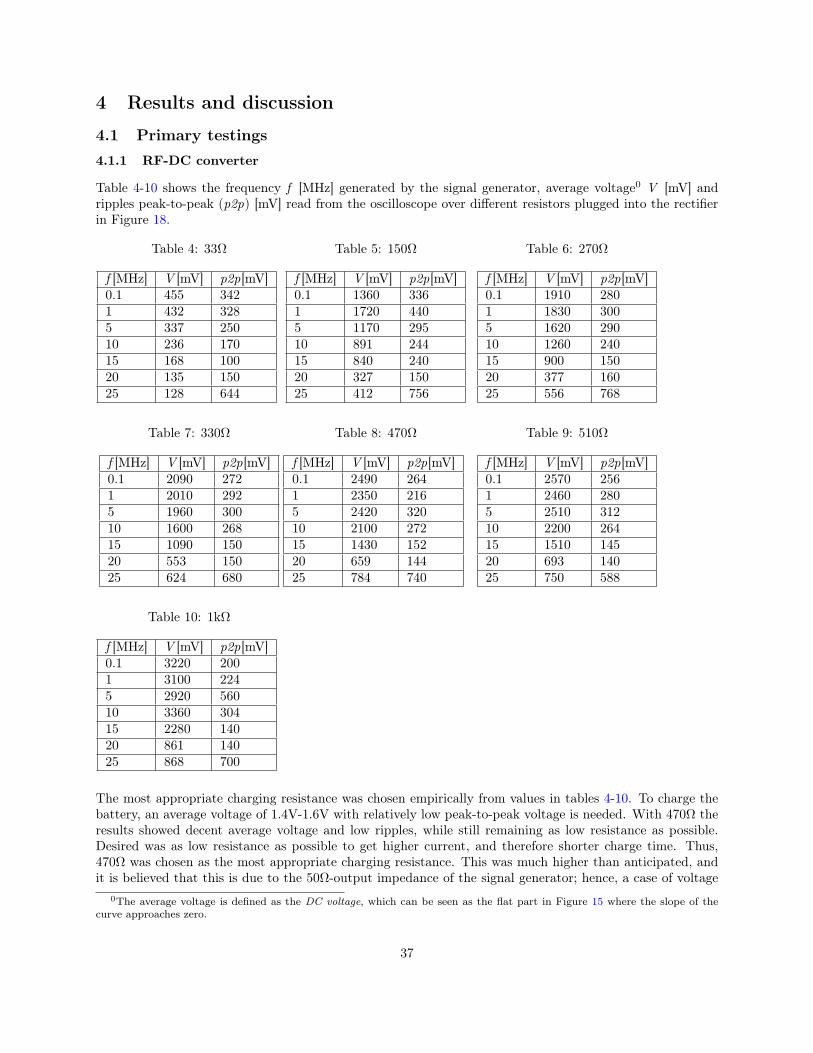
Figure 32: Rectifier output with 470Ω load and 11.5MHz input. This is the DC part of the curve, similar tothe flat part of Figure 15.
Observe that the ripples in Figure 32 does not look like the ones in Figure 15. This might be because therealized rectifier operates at 11.5 MHz whilst the simulated one operates at 140 MHz. Perhaps the reasonfor the difference in operating frequency is the diodes. One potential problem, is the differing output powerof the signal generator. Since our diodes need a voltage drop of sufficing magnitude to be forward-biased, adiffering power output can create situations where we have too low voltage which could be the case when weraise frequency above a certain threshold. Additionally, not all diodes are the same. Schottky diodes werechosen because of their low forward-biasing and faster twitching speed, which makes them favorable for high-frequency circuits. However, there are different models of Schottky diodes and therefore the specificationsvary. Our kind, the 1N5817-diode, has a forward-bias of 0.45-0.75 V, depending on the forward current. Onthe data sheet, seen in Appendix Data Sheet B.2, it says it is has "extremely fast switching" and features"high frequency operation". On account of the aforementioned, the diode should be able to operate in theconditions that we pose, but is also dependent of what the manufacturer classes as high frequency. Multiplesources claim that Schottky-diodes works well for "multiple MHz", but doesn’t specify what range thatis. Hence, one should consider if Schottky-diodes really was the optimal diode choice for this application.Other perhaps more suitable choices for further realization could be tunnel diodes that can operate at upto multiple GHz or IMPATT diodes which is used in HF microwave devices. A downside to these type ofdiodes is that they’re quite expensive.
38
4.1.2 Battery discharge
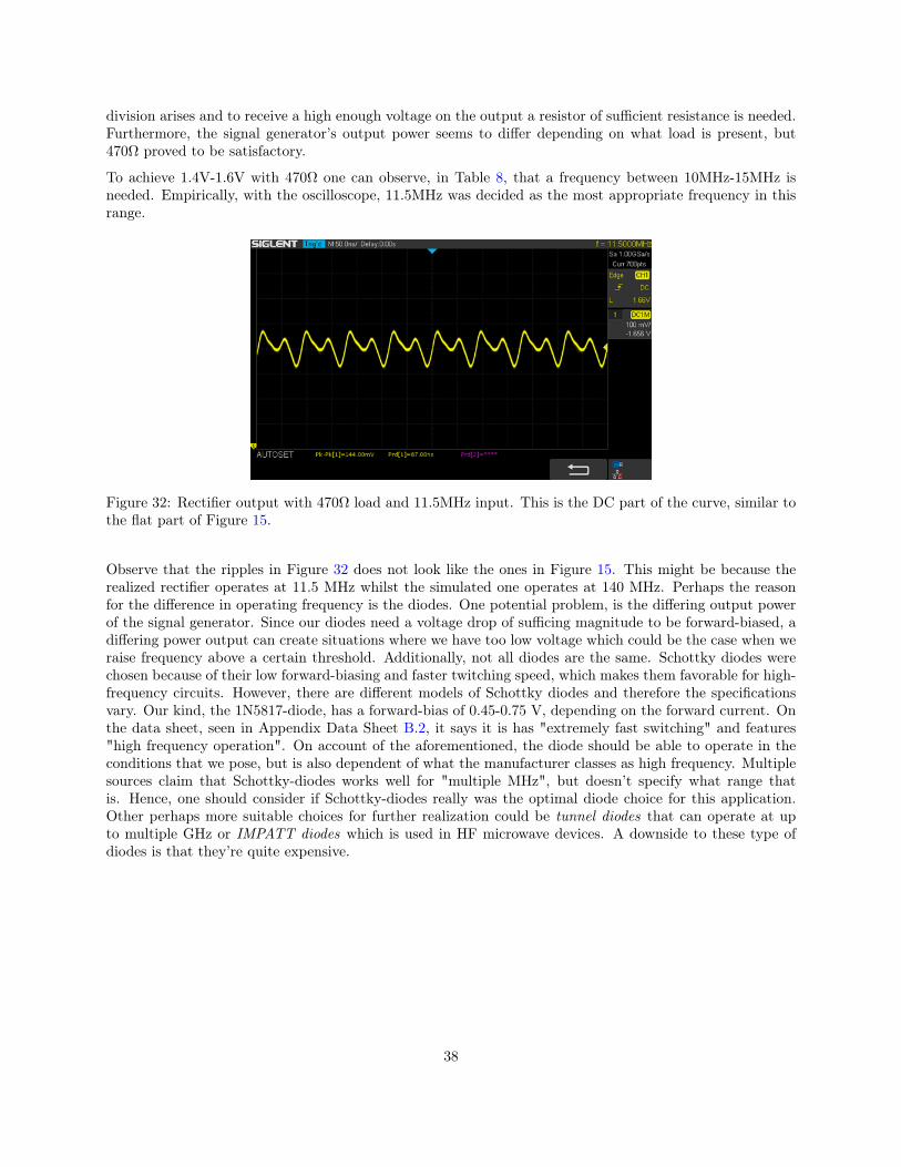
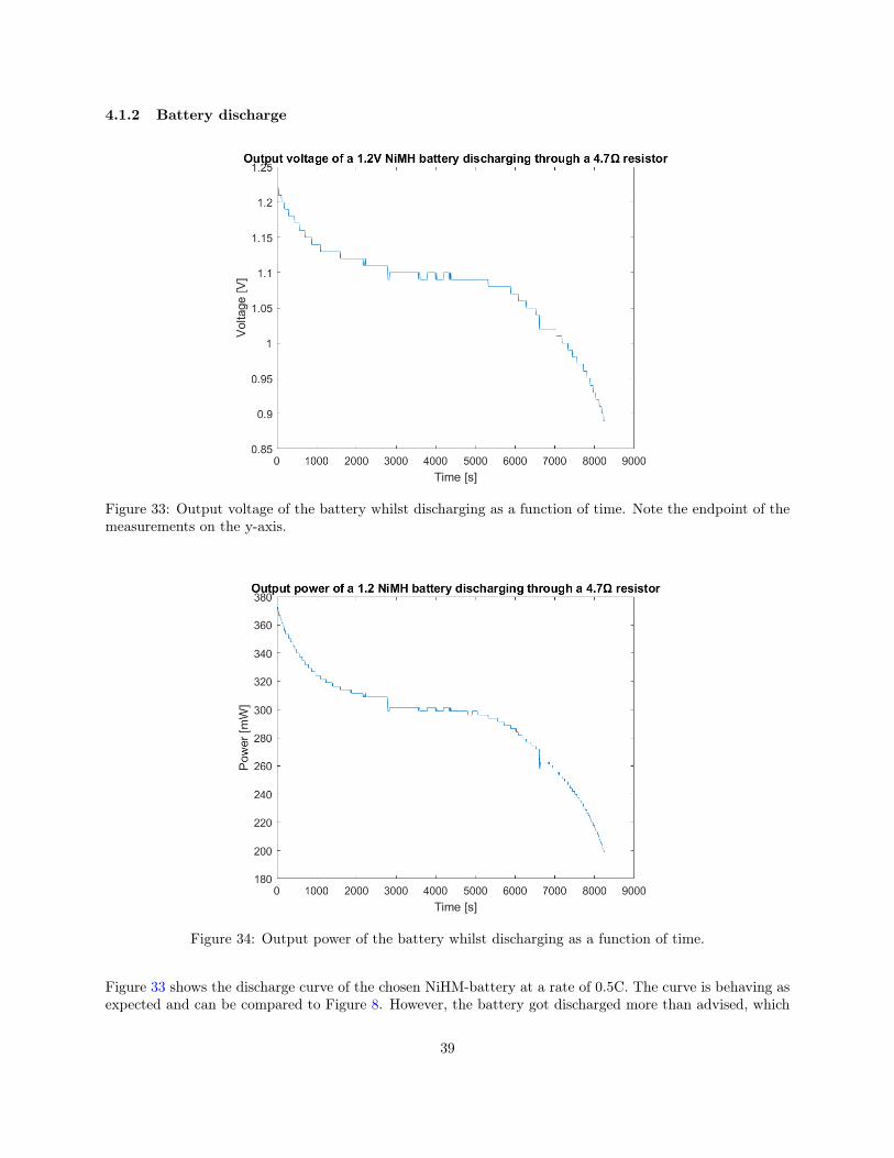
Figure 33: Output voltage of the battery whilst discharging as a function of time. Note the endpoint of themeasurements on the y-axis.
Figure 34: Output power of the battery whilst discharging as a function of time.
Figure 33 shows the discharge curve of the chosen NiHM-battery at a rate of 0.5C. The curve is behaving asexpected and can be compared to Figure 8. However, the battery got discharged more than advised, which
39
could have damaged the battery.
4.1.3 Battery recharge
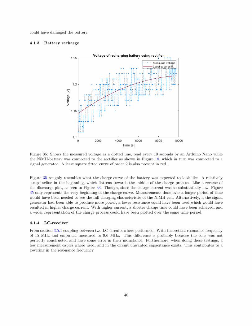
Figure 35: Shows the measured voltage as a dotted line, read every 10 seconds by an Arduino Nano whilethe NiMH-battery was connected to the rectifier as shown in Figure 18, which in turn was connected to asignal generator. A least square fitted curve of order 2 is also present in red.
Figure 35 roughly resembles what the charge-curve of the battery was expected to look like. A relativelysteep incline in the beginning, which flattens towards the middle of the charge process. Like a reverse ofthe discharge plot, as seen in Figure 33. Though, since the charge current was so substantially low, Figure35 only represents the very beginning of the charge-curve. Measurements done over a longer period of timewould have been needed to see the full charging characteristic of the NiMH cell. Alternatively, if the signalgenerator had been able to produce more power, a lower resistance could have been used which would haveresulted in higher charge current. With higher current, a shorter charge time could have been achieved, anda wider representation of the charge process could have been plotted over the same time period.
4.1.4 LC-receiver
From section 3.5.1 coupling between two LC-circuits where performed. With theoretical resonance frequencyof 15 MHz and empirical measured to 9.6 MHz. This difference is probably because the coils was notperfectly constructed and have some error in their inductance. Furthermore, when doing these testings, afew measurement cables where used, and in the circuit unwanted capacitance exists. This contributes to alowering in the resonance frequency.
40
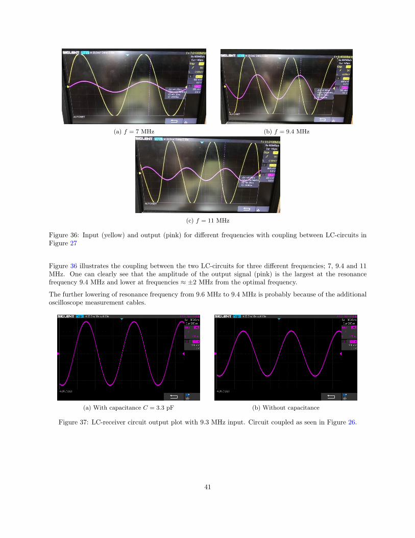
(a) f = 7 MHz (b) f = 9.4 MHz
(c) f = 11 MHz
Figure 36: Input (yellow) and output (pink) for different frequencies with coupling between LC-circuits inFigure 27
Figure 36 illustrates the coupling between the two LC-circuits for three different frequencies; 7, 9.4 and 11MHz. One can clearly see that the amplitude of the output signal (pink) is the largest at the resonancefrequency 9.4 MHz and lower at frequencies ≈ ±2 MHz from the optimal frequency.
The further lowering of resonance frequency from 9.6 MHz to 9.4 MHz is probably because of the additionaloscilloscope measurement cables.
(a) With capacitance C = 3.3 pF (b) Without capacitance
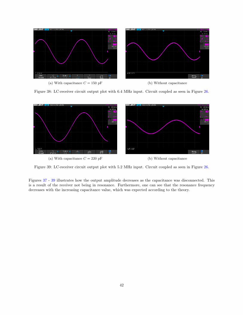
Figure 37: LC-receiver circuit output plot with 9.3 MHz input. Circuit coupled as seen in Figure 26.
41
(a) With capacitance C = 150 pF (b) Without capacitance
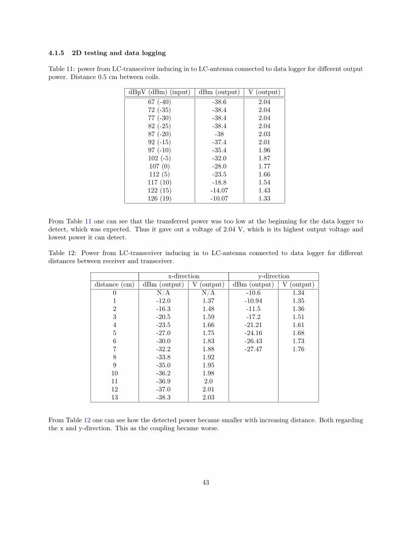
Figure 38: LC-receiver circuit output plot with 6.4 MHz input. Circuit coupled as seen in Figure 26.
(a) With capacitance C = 220 pF (b) Without capacitance
Figure 39: LC-receiver circuit output plot with 5.2 MHz input. Circuit coupled as seen in Figure 26.
Figures 37 - 39 illustrates how the output amplitude decreases as the capacitance was disconnected. Thisis a result of the receiver not being in resonance. Furthermore, one can see that the resonance frequencydecreases with the increasing capacitance value, which was expected according to the theory.
42
4.1.5 2D testing and data logging
Table 11: power from LC-transceiver inducing in to LC-antenna connected to data logger for different outputpower. Distance 0.5 cm between coils.
dBµV (dBm) (input) dBm (output) V (output)67 (-40) -38.6 2.0472 (-35) -38.4 2.0477 (-30) -38.4 2.0482 (-25) -38.4 2.0487 (-20) -38 2.0392 (-15) -37.4 2.0197 (-10) -35.4 1.96102 (-5) -32.0 1.87107 (0) -28.0 1.77112 (5) -23.5 1.66117 (10) -18.8 1.54122 (15) -14.07 1.43126 (19) -10.07 1.33
From Table 11 one can see that the transferred power was too low at the beginning for the data logger todetect, which was expected. Thus it gave out a voltage of 2.04 V, which is its highest output voltage andlowest power it can detect.
Table 12: Power from LC-transceiver inducing in to LC-antenna connected to data logger for differentdistances between receiver and transceiver.
x-direction y-directiondistance (cm) dBm (output) V (output) dBm (output) V (output)
0 N/A N/A -10.6 1.341 -12.0 1.37 -10.94 1.352 -16.3 1.48 -11.5 1.363 -20.5 1.59 -17.2 1.514 -23.5 1.66 -21.21 1.615 -27.0 1.75 -24.16 1.686 -30.0 1.83 -26.43 1.737 -32.2 1.88 -27.47 1.768 -33.8 1.929 -35.0 1.9510 -36.2 1.9811 -36.9 2.012 -37.0 2.0113 -38.3 2.03
From Table 12 one can see how the detected power became smaller with increasing distance. Both regardingthe x and y-direction. This as the coupling became worse.
43
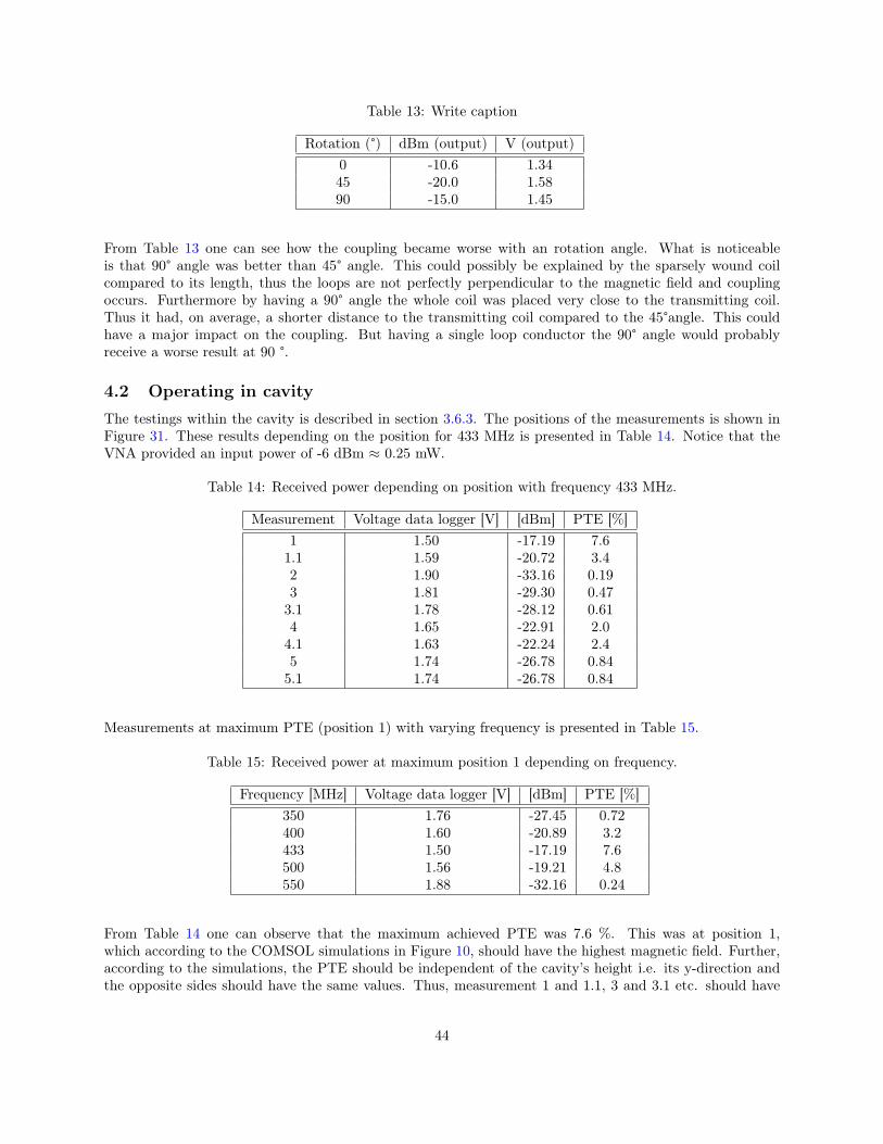
Table 13: Write caption
Rotation (°) dBm (output) V (output)0 -10.6 1.3445 -20.0 1.5890 -15.0 1.45
From Table 13 one can see how the coupling became worse with an rotation angle. What is noticeableis that 90° angle was better than 45° angle. This could possibly be explained by the sparsely wound coilcompared to its length, thus the loops are not perfectly perpendicular to the magnetic field and couplingoccurs. Furthermore by having a 90° angle the whole coil was placed very close to the transmitting coil.Thus it had, on average, a shorter distance to the transmitting coil compared to the 45°angle. This couldhave a major impact on the coupling. But having a single loop conductor the 90° angle would probablyreceive a worse result at 90 °.
4.2 Operating in cavityThe testings within the cavity is described in section 3.6.3. The positions of the measurements is shown inFigure 31. These results depending on the position for 433 MHz is presented in Table 14. Notice that theVNA provided an input power of -6 dBm ≈ 0.25 mW.
Table 14: Received power depending on position with frequency 433 MHz.
Measurement Voltage data logger [V] [dBm] PTE [%]1 1.50 -17.19 7.61.1 1.59 -20.72 3.42 1.90 -33.16 0.193 1.81 -29.30 0.473.1 1.78 -28.12 0.614 1.65 -22.91 2.04.1 1.63 -22.24 2.45 1.74 -26.78 0.845.1 1.74 -26.78 0.84
Measurements at maximum PTE (position 1) with varying frequency is presented in Table 15.
Table 15: Received power at maximum position 1 depending on frequency.
Frequency [MHz] Voltage data logger [V] [dBm] PTE [%]350 1.76 -27.45 0.72400 1.60 -20.89 3.2433 1.50 -17.19 7.6500 1.56 -19.21 4.8550 1.88 -32.16 0.24
From Table 14 one can observe that the maximum achieved PTE was 7.6 %. This was at position 1,which according to the COMSOL simulations in Figure 10, should have the highest magnetic field. Further,according to the simulations, the PTE should be independent of the cavity’s height i.e. its y-direction andthe opposite sides should have the same values. Thus, measurement 1 and 1.1, 3 and 3.1 etc. should have
44
the same value. From Table 15 one can observe that this is the tendency. However 1 and 1.1 have ratherlarge difference while 5 and 5.1 is exactly the same.
Measurements were also performed at the other side walls and similar results was obtained in accordancewith the simulations. Thus the H-field pattern seems to be similar. However a few things were noticed thataffected the results and contributed to errors.
The perturbation object used to lower the resonance frequency was placed in the middle of the cavity. Ifthis was not placed in the middle or if it was not uniform it affected the fields which led to not same PTEat the opposite walls. The object was also rather big which could affect the fields. Ideally the cavity shouldhave been slightly larger to lower the fundamental resonance frequency. Furthermore, where the antenna wasplaced and its downward-angle affected the results. Ideally it should be mounted in the middle and pointdownwards. As the lid of the cavity had to be removed between each measurement this was difficult to keepconsistent. Also the receiving coil had to be mounted at the exact position and angle. For instance whenvarying the height (y-direction) the x and z were probably not the exact same nor was the angle. Thoughat the corner it was easier to be consistent and the same results for 5, 5.1 was obtained.
Measurement 2 received the worst PTE. According to the simulations, the loop’s cross section was mountedin parallel to the magnetic field. Thus, ideally, no PTE should have been achieved, but the result indicate amagnetic field direction in accordance with the simulations.
Table 15 shows how the PTE was affected as the frequency was decreased and increased from the optimalvalue of 433 MHz. If Figure 30 is observed. At 400 and 500 MHz there is still some reduction of the reflectedpower to the source, While at 350 and 550 MHz there is barley any resonance. This clearly illustrates theimportance of the cavity being in resonance.
As mentioned, it was hard to determine the resonance frequency of the receiving LC-circuit antenna andit probably had a higher resonance frequency. This as the construction was hard to do precise. However,what could be observed trying to measure the resonance frequency of the LC-receiver was that it had avery narrow resonance band. Thus, its resonance frequency had to be at exactly 433 MHz to receive goodcoupling. If this would have been achieved, a higher PTE would have been expected.
Since the reciving coil was very small compared to the cavity resonare, the PTE was decreased. As the cavitycan be modeled as a LC-circuit, one can model the coupling between the cavity and the receiving antennaas two coils with a large size difference. Consequently, the coupling between them is poor. Ideally, the loopwould be big and resonate at the correct frequency, which are both hard to achieve at high frequencies.To further maximize the PTE, one could take impedance matching into consideration. This has not beenapplied because of complexity using it in every steps.
In this cavity resonator only one mode, the TE101 mode was excited. This led to a H-field distributionwith low values at some locations. Powering devices anywhere inside the cavity, high PTE is desired at anylocation. This could be achieved by exciting multiple modes i.e. a multimode cavity. However doing this,the problem of the receivers being resonant for a wide range of frequencies occurs.
45
5 ConclusionAll of the smaller sub goals were implemented with varying results, some favorable, some not. A RF-to-DCrectifier was constructed that received an RF signal from the signal generator, which it then rectified toproduce a DC output with relatively small ripples. The rectifier worked very well for lower radio frequencies(30 kHz to 12 MHz), but failed for higher frequencies (>13 MHz). The conclusion is that it is due to poorperformance of the Schottky diodes for high frequency operations, and that the rectifier should work forthese frequencies if different diodes would have been used (e.g. tunnel or IMPATT diodes). Unfortunately,the discovery was made too late because of lab restrictions due to COVID-19, and the shipping time wouldoverstep the time limit for the project. Additionally, it may be that the rectifier would have worked with ahigher input power, but there was no power amplifier, or signal generator, with larger output amplitude toborrow.
Next, several tests were done on AAA NiMH batteries to study their discharge and recharge curves. Adischarge curve was found which looked very similar to existing theory on these. Since the RF-to-DCrectifier would not work for 433 MHz, it was decided to attempt recharging with the constructed rectifierconnected to a signal generator which provided an output of 126 dBµV at 11.5 MHz. The voltage of thebattery was tracked by an Arduino Nano. Using a least squares fit to our data showed a distinct trend,which looked similar to known recharge curves of NiMH batteries. To establish a more reliable conclusion,that the batteries can be fully charged by our rectifier, one would have to run the recharge test longer (morethan the current 3 hours). However, current measurements indicates that it works.
The last three sub goals were closely intertwined. A cavity resonator out of aluminum was built with afundamental resonating frequency of around 470 MHz. Then, COMSOL simulations were done to see howthe TE101 field would be distributed inside a cavity of the dimensions given by the constructed aluminumbox. Thereafter, a series of 2D tests with coils were conducted to confirm that the ZX-47 RF power detectorworked as intended, which it did. Then a case for the power detector was 3D-printed, to facilitate the useof it inside a cavity and to prevent any potential damage to it. Furthermore, an LC-circuit was constructedto be used as an antenna to the RF power detector, to be able to pick up signals inside the resonant cavity.The antenna was built in such a way that it should have resonated in the same frequency as the cavity,but testings suggested that the antenna resonated at a slightly higher frequency. This was perhaps due toa coil which did not have the correct dimensions; a more precise method of building coils was needed, ormaybe tools designed for that purpose. Lastly, the RF power detector with the antenna attached was movedaround in the cavity whilst excited with 433 MHz signals. The results show a field distribution similar tothe simulations in COMSOL. The testings showed that 7.6% was the highest percentage picked up by theantenna compared to the source. Further testings that would have been interesting is using different sizedcoils in the LC-antenna to see how it correlates to magnetic field coupling. Additionally, to charge multipledevices at the same time inside the cavity one would have to look into the use of multimode to obtain a fielddistribution which is more favorable; hence, a higher frequency would be used.
There was several limitations posed on us during this project. Due to COVID-19, access to the electroniclabs at Ångström was restricted and therefore there was a shortage of equipment needed; the group had tomake do with the material that was possible to borrow. Several delays emerged because of shipping times,which in turn decreased the time available to do realisations and testing of the material. Despite all of this,every sub goal was realized with some favorable results, and some not.
46

References[1] “Understanding rf signals.” http://etutorials.org/Networking/wn/Chapter+3.+Radio+Frequency+
and+Light+Signal+Fundamentals+The+Invisible+Medium/Understanding+RF+Signals/, [obtained2021-04-17].
[2] “Wireless power transfer history and state-of-the-art.” https://wpt.ieee.org/wpt-history/, 2021[obtained 2021-04-21].
[3] H. Mei, K. A. Thackston, R. A. Bercich, J. G. Jefferys, and P. P. Irazoqui, “Cavity resonator wire-less power transfer system for freely moving animal experiments,” IEEE Transactions on BiomedicalEngineering, vol. 64, no. 4, pp. 775–785, 2016.
[4] M. Shahmohammadi, M. J. Chabalko, and A. P. Sample, “Circuit model for resonant cavity modeenabled wireless power transfer,” in 2016 46th European Microwave Conference (EuMC), pp. 747–750,IEEE, 2016.
[5] “Amazon prime air.” https://www.amazon.com/Amazon-Prime-Air/b?ie=UTF8&node=8037720011,[obtained 2021-04-26].
[6] S. W. Ellingson, “6.8: Rectangular waveguide- tm modes.” https://phys.libretexts.org/Bookshelves/Electricity_and_Magnetism/Book%3A_Electromagnetics_II_(Ellingson)/06%3A_Waveguides/6.08%3A_Rectangular_Waveguide-_TM_Modes, 2020 [obtained 2021-04-16].
[7] D. M. Pozar, Microwave engineering. John wiley & sons, 2011.
[8] M. Mehdizadeh, Microwave/RF Applicators and Probes 2nd Edition. Elsevier, 2015.
[9] R. A. Alvarez, “Microwave energy storage in resonant cavities,” University of California, 1983.
[10] M. J. Chabalko and A. P. Sample, “Three-dimensional charging via multimode resonant cavity enabledwireless power transfer,” IEEE Transactions on Power Electronics, vol. 30, no. 11, pp. 6163–6173, 2015.
[11] “Excitation of cavity resonator.” https://www.daenotes.com/electronics/microwave-radar/excitation-methods-of-cavity-resonator, [obtained 2021-05-15].
[12] “Cavity perturbation theory.” https://en.wikipedia.org/wiki/Cavity_perturbation_theory, 2021[obtained 2021-05-01].
[13] “Frequently asked questions - itu.” https://www.itu.int/net/ITU-R/terrestrial/faq/index.html,[obtained 2021-05-16].
[14] “Selected european radio frequency allocations 30 mhz to 300 ghz.” https://www.rfcafe.com/references/electrical/rf-freq-allo-euro.htm, [obtained 2021-04-15].
[15] L. Frenzel, “Back to basics: Impedance matching (part 1).” https://www.electronicdesign.com/technologies/communications/article/21796367/back-to-basics-impedance-matching-part-1, 2011 [obtained: 2021-04-05].
[16] “Coefficient of coupling.” https://circuitglobe.com/what-is-coefficient-of-coupling.html,[obtained 2021-04-15].
[17] “Oscillations in an lc circuit.” https://phys.libretexts.org/@go/page/4439, 2020 [obtained 2021-04-10].
[18] C. R. Paul, Inductance: loop and partial. John Wiley & Sons, 2011.
[19] CC.B.Honsberg and S.G.Bowden, “Photovoltaics education website.” www.pveducation.org, 2019 [ob-tained 2021-04-10].
[20] “Learning about electronics.” http://www.learningaboutelectronics.com, [obtained 2021-04-13].
47

[21] J. Garche, C. K. Dyer, P. T. Moseley, Z. Ogumi, D. A. Rand, and B. Scrosati, Encyclopedia of electro-chemical power sources. Newnes, 2013.
[22] M. Venis, “Testing nicd and nimh batteries.” https://www.ebme.co.uk/articles/maintenance/testing-nicd-and-nimh-batteries, [obtained 2021-04-20].
[23] “What is arduino?.” https://www.arduino.cc/en/Guide/Introduction, [obtained 2021-04-19].
[24] “Arduino reference.” https://www.arduino.cc/reference/en/, [obtained 2021-04-19].
[25] “Read analog voltage.” https://www.arduino.cc/en/Tutorial/BuiltInExamples/ReadAnalogVoltage, [obtained 2021-04-19].
[26] “What is a vector network analyzer, vna: the basics.” https://www.electronics-notes.com/articles/test-methods/rf-vector-network-analyzer-vna/what-is-a-vna.php, [obtained 2021-05-19].
[27] “Em mode analysis for the rectangular waveguide | comsol multiphysics tutorial-5.” https://www.youtube.com/watch?v=u5zNmwLT5Bc, 2018 [obtained 2021-04-12].
[28] “How to model and simulate 3d geometry? | comsol multiphysics tutorial-2.” https://www.youtube.com/watch?v=fKwm6NFQcms, 2018 [obtained 2021-04-22].
[29] T. Thakuria, H. K. Singh, and T. Bezboruah, “Modelling and simulation of low cost rf energy har-vesting system,” in 2017 International Conference on Innovations in Electronics, Signal Processing andCommunication (IESC), pp. 51–54, IEEE, 2017.
[30] “The seven top uses for rechargeable lithium-ion batteries.” https://relionbattery.com/blog/the-seven-top-uses-for-rechargeable-lithium-ion-batteries, 2015 [obtained 2021-05-03].
[31] “What’s the best battery?.” https://batteryuniversity.com/learn/archive/whats_the_best_battery, 2017 [obtained: 2021-05-03 ].
[32] “Uppladdningsbara aaa-batterier hr03 1,2v 500 mah.” https://www.netonnet.se/art/hem-hushall/batterier/laddningsbara-batterier/andersson-laddningsbara-aaa-batterier-hr03-12v-500mah/1008896.9455/, [obtained 2021-04-14].
[33] “Nimh battery charging basics.” https://www.powerstream.com/NiMH.htm, 2021 [obtained 2021-05-05].
[34] L. E. Frenzel, “Rf detectors for wireless devices.” https://www.analog.com/media/en/technical-documentation/frequently-asked-questions/201551981Detector_FAQ.pdf, [obtained2021-04-27].
[35] “Making a 10w linear - part 3 - directional coupler.” https://www.youtube.com/watch?v=T6_NHJHSwq0&t=308s, 2020 [obtained: 2021-04-12].
[36] “Wireless charger | theory & homemade circuit.” https://www.youtube.com/watch?v=eNZ8KPHYDvg&t=239s, 2021 [obtained 2021-04-09].
48

Appendix A: Code
Appendix A.1: Charge/Discharge// Charge/Discharge code
const float referenceVolts = 4.66; // Calibrated reference voltgeconst int sensorPin = A0; // Connected to analog pin A0const int sensorPin2 = A2; // Connected to analog pin A2int ReadVal = 0; // varible to store read valueint ReadVal2 = 0;int resistance = 470; // The resistance measured over (4.7 for discharge)
float volts = 0;float volts2 = 0;float current = 0;float power = 0;
//-------------------------------------------------------------------------------
void setup()pinMode(sensorPin , INPUT);pinMode(sensorPin2 , INPUT);Serial.begin (9600);
Serial.print ("Time since start [s]: ");Serial.print (" Voltage [V]: ");Serial.print (" Voltage2 [V]: ");Serial.print (" Current [mA]: ");Serial.print ("Power [mW]: ");Serial.print ("\n");
//--------------------------------------------------------------------------------
void Calculations(int ReadVal ,int Readval2)
volts = (ReadVal / 1023.0) * referenceVolts; // Calculate the ratiovolts2 = (ReadVal2 / 1023.0) * referenceVolts;current = 1000*( volts / resistance ); // [mA]
//---------------------------------------------------------------------------------
void ReadPower ()
const unsigned long ReadTimeInterval = 100; // ms // First 3 rows changed depending on display intervalconst int NumSamples = 300; // msconst unsigned long CalcTimeInterval = 30000; // msstatic unsigned long CurrentTime = 0;static unsigned long LastReadTime = 0;static unsigned long LastCalcTime = 0;static int ReadValArray[NumSamples ];static long int ReadValAve = 0;static int ReadValArray2[NumSamples ];static long int ReadValAve2 = 0;static int ArrayIndex = 0;
CurrentTime = millis (); // Time since started
if(CurrentTime - LastReadTime >= ReadTimeInterval) // Take reading every ReadTimeInterval
LastReadTime += ReadTimeInterval;ReadVal = analogRead(sensorPin ); // Read the value from the sensorReadVal2 = analogRead(sensorPin2 ); // Read the value from the sensor
ReadValArray[ArrayIndex] = ReadVal;ReadValArray2[ArrayIndex] = ReadVal2;if (ArrayIndex < NumSamples - 1)
ArrayIndex = ArrayIndex + 1;else
ArrayIndex = 0;
49
if(CurrentTime - LastCalcTime >= CalcTimeInterval)
LastCalcTime += CalcTimeInterval; // Update time when doing calculationReadValAve = 0; // Reset the average valueReadValAve2 = 0;
for (int Index = 0; Index <= NumSamples -1; Index ++)
ReadValAve = ReadValAve + ReadValArray[Index ];ReadValAve2 = ReadValAve2 + ReadValArray2[Index ];
ReadValAve = ReadValAve / NumSamples; // Calculate avarageReadValAve2 = ReadValAve2 / NumSamples;
Calculations(ReadValAve , ReadValAve2 );
Serial.print(CurrentTime /1000);Serial.print (" ");Serial.print(volts2 );Serial.print (" ");Serial.print(volts);Serial.print (" ");Serial.print(current );Serial.print (" ");Serial.print(current*volts);Serial.print (" ");Serial.print ("\n");
//---------------------------------------------------------------------------------
void loop()
ReadPower ();
50
Appendix A.2: Data logger
//Power detector data logger code
const float referenceVolts = 4.3; // calibrated reference voltageconst int sensorPin = A6; // power detector is connected to analog pin A6int ReadVal = 0; // varible to store read valueint freq; // variable to store the frequency inputint k;int m;int dBm_to_power;
float volts = 0;float dBm = 0;double power = 0;
//-------------------------------------------------------------------------------
void setup()pinMode(sensorPin , INPUT);Serial.begin (9600);Serial.println ("What frequency is used? (MHz )"); // Prompt User for Inputwhile (Serial.available () == 0) // Wait for user to input frequencyfreq = Serial.parseInt (); // Read the data the user has input
Serial.print (" Output DC [V]: ");Serial.print ("Input power [dBm]: ");Serial.print ("Input power [mW]: ");Serial.print ("\n");
if ((freq >= 10) && (freq < 1000)) // Different curves for different frequenciesk = -40.9 + (freq /10000); // Create smooth transitions between frequenciesm = 43.1 - (freq /770); // Starts at -40.9*V + 43.1
// Ends at -40.8*V + 41.8
if ((freq >= 1000) && (freq < 2000)) k = -41.2 + (freq /2500); // Starts at -40.8*V + 41.8m = 43.8 - (freq /500); // Ends at -40.4*V + 39.8
if ((freq >= 2000) && (freq < 5000)) k = -40.65 + (freq /8000); // Starts at -40.4*V + 39.8m = 38.4 + (freq /1400) // Ends at -40.0*V + 42.0
//--------------------------------------------------------------------------------
void CalculatePower(int ReadVal)
volts = (ReadVal / 1023.0) * referenceVolts; // Calculate the ratiodBm = (volts * k + m); // dBm based on linear regressions
power = pow(10, (dBm /10)); // From dBm to power [mW]
//---------------------------------------------------------------------------------
void ReadPower ()
const unsigned long ReadTimeInterval = 10; // Take reading every 10 [ms]const int NumSamples = 200;//100; // [ms]const unsigned long CalcTimeInterval = 2000;//1000; // [ms]static unsigned long CurrentTime = 0;static unsigned long LastReadTime = 0;static unsigned long LastCalcTime = 0;static int ReadValArray[NumSamples ];static long int ReadValAve = 0;static int ArrayIndex = 0;
CurrentTime = millis (); // Time since started
if(CurrentTime - LastReadTime >= ReadTimeInterval) // Take reading every ReadTimeInterval
51
LastReadTime += ReadTimeInterval;ReadVal = analogRead(sensorPin ); // Read the value from the sensor
ReadValArray[ArrayIndex] = ReadVal;
if (ArrayIndex < NumSamples - 1)ArrayIndex = ArrayIndex + 1;
elseArrayIndex = 0;
if(CurrentTime - LastCalcTime >= CalcTimeInterval)
LastCalcTime += CalcTimeInterval; // Update time when doing calculationReadValAve = 0; // Reset the average value
for (int Index = 0; Index <= NumSamples -1; Index ++)
ReadValAve = ReadValAve + ReadValArray[Index ];
ReadValAve = ReadValAve / NumSamples; // Calculate avarage
CalculatePower(ReadValAve );
Serial.print(volts);Serial.print (" ");Serial.print(dBm);Serial.print (" ");Serial.print(power);Serial.print ("\n");
//---------------------------------------------------------------------------------
void loop()
ReadPower ();
52

Appendix B: Data Sheets
Appendix B.1: ZX47-40LN-S+ RF Power Detector
53
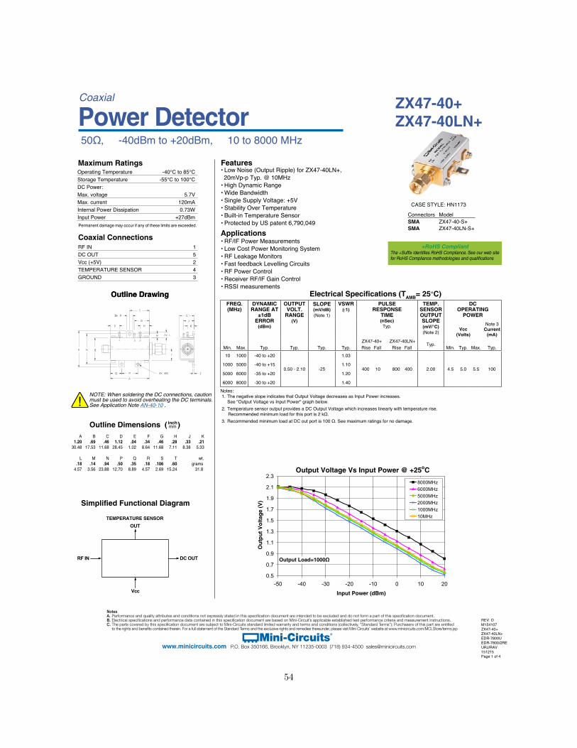
NotesA. Performance and quality attributes and conditions not expressly stated in this specification document are intended to be excluded and do not form a part of this specification document. B. Electrical specifications and performance data contained in this specification document are based on Mini-Circuit’s applicable established test performance criteria and measurement instructions. C. The parts covered by this specification document are subject to Mini-Circuits standard limited warranty and terms and conditions (collectively, “Standard Terms”); Purchasers of this part are entitled to the rights and benefits contained therein. For a full statement of the Standard Terms and the exclusive rights and remedies thereunder, please visit Mini-Circuits’ website at www.minicircuits.com/MCLStore/terms.jsp
Mini-Circuits®
www.minicircuits.com P.O. Box 350166, Brooklyn, NY 11235-0003 (718) 934-4500 [email protected]
REV. DM154107ZX47-40+ZX47-40LN+EDR-7800UEDR-7800/2REURJ/RAV151215Page 1 of 4
Operating Temperature -40°C to 85°C Storage Temperature -55°C to 100°CDC Power:Max. voltage 5.7VMax. current 120mAInternal Power Dissipation 0.73WInput Power +27dBm
CASE STYLE: HN1173
Notes: 1. The negative slope indicates that Output Voltage decreases as Input Power increases. See "Output Voltage vs Input Power" graph below.
2. Temperature sensor output provides a DC Output Voltage which increases linearly with temperature rise.Recommended minimum load for this port is 2 kΩ.
3. Recommended minimum load at DC out port is 100 Ω. See maximum ratings for no damage.
Connectors ModelSMA ZX47-40-S+SMA ZX47-40LN-S+
Maximum Ratings
Electrical Specifications (TAMB= 25°C)
• Low Noise (Output Ripple) for ZX47-40LN+, 20mVp-p Typ. @ 10MHz • High Dynamic Range• Wide Bandwidth• Single Supply Voltage: +5V• Stability Over Temperature• Built-in Temperature Sensor• Protected by US patent 6,790,049
Features
• RF/IF Power Measurements• Low Cost Power Monitoring System• RF Leakage Monitors• Fast feedback Levelling Circuits• RF Power Control• Receiver RF/IF Gain Control• RSSI measurements
Applications
ZX47-40+ ZX47-40LN+Power Detector
50Ω, -40dBm to +20dBm, 10 to 8000 MHz
Coaxial
Output Voltage Vs Input Power @ +25oC
0.5
0.7
0.9
1.1
1.3
1.5
1.7
1.9
2.1
2.3
-50 -40 -30 -20 -10 0 10 20
Input Power (dBm)
Out
put V
olta
ge (V
)
8000MHz6000MHz5000MHz2000MHz1000MHz10MHz
Outline Drawing
A B C D E F G H J K 1.20 .69 .46 1.12 .04 .34 .46 .28 .33 .21 30.48 17.53 11.68 28.45 1.02 8.64 11.68 7.11 8.38 5.33
Outline Dimensions ( )inchmm
L M N P Q R S T wt. .18 .14 .94 .50 .35 .18 .106 .60 grams 4.57 3.56 23.88 12.70 8.89 4.57 2.69 15.24 31.8
Simplified Functional Diagram
RF IN 1DC OUT 5Vcc (+5V) 2TEMPERATURE SENSOR 4GROUND 3
Coaxial Connections
TEMP SENSOR OUT
RF IN
Vcc
DC OUT
TEMPERATURE SENSOR
Output Load=1000Ω
FREQ.(MHz)
DYNAMICRANGE AT
±1dBERROR
(dBm)
OUTPUTVOLT.
RANGE(V)
SLOPE(mV/dB)(Note 1)
VSWR(:1)
PULSERESPONSE
TIME(nSec)
Typ.
TEMP.SENSOROUTPUTSLOPE(mV/°C)(Note 2)
DCOPERATING
POWER
Vcc(Volts)
Note 3Current
(mA)
Min. Max. Typ. Typ. Typ. Typ.ZX47-40+ ZX47-40LN+
Typ.Min. Typ. Max. Typ.Rise Fall Rise Fall
10 1000 -40 to +20
0.50 - 2.10 -25
1.03
400 10 800 400 2.00 4.5 5.0 5.5 1001000 5000 -40 to +15 1.10
5000 6000 -35 to +20 1.20
6000 8000 -30 to +20 1.40
Permanent damage may occur if any of these limits are exceeded.
Outline Drawing
+RoHS CompliantThe +Suffix identifies RoHS Compliance. See our web site for RoHS Compliance methodologies and qualifications
NOTE: When soldering the DC connections, caution must be used to avoid overheating the DC terminals. See Application Note AN-40-10 .!
54
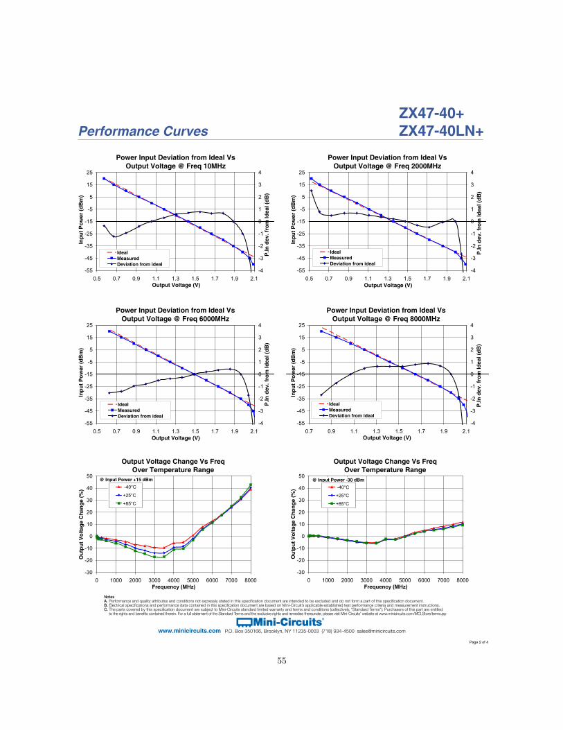
NotesA. Performance and quality attributes and conditions not expressly stated in this specification document are intended to be excluded and do not form a part of this specification document. B. Electrical specifications and performance data contained in this specification document are based on Mini-Circuit’s applicable established test performance criteria and measurement instructions. C. The parts covered by this specification document are subject to Mini-Circuits standard limited warranty and terms and conditions (collectively, “Standard Terms”); Purchasers of this part are entitled to the rights and benefits contained therein. For a full statement of the Standard Terms and the exclusive rights and remedies thereunder, please visit Mini-Circuits’ website at www.minicircuits.com/MCLStore/terms.jsp
Mini-Circuits®
www.minicircuits.com P.O. Box 350166, Brooklyn, NY 11235-0003 (718) 934-4500 [email protected]
Page 2 of 4
Performance CurvesZX47-40+ZX47-40LN+
Power Input Deviation from Ideal VsOutput Voltage @ Freq 2000MHz
-55
-45
-35
-25
-15
-5
5
15
25
0.5 0.7 0.9 1.1 1.3 1.5 1.7 1.9 2.1Output Voltage (V)
Inpu
t Pow
er (d
Bm
)
-4
-3
-2
-1
0
1
2
3
4
P.In
dev
. fro
m Id
eal (
dB)
IdealMeasuredDeviation from ideal
Power Input Deviation from Ideal VsOutput Voltage @ Freq 6000MHz
-55
-45
-35
-25
-15
-5
5
15
25
0.5 0.7 0.9 1.1 1.3 1.5 1.7 1.9 2.1Output Voltage (V)
Inpu
t Pow
er (d
Bm
)
-4
-3
-2
-1
0
1
2
3
4
P.In
dev
. fro
m Id
eal (
dB)
IdealMeasuredDeviation from ideal
Power Input Deviation from Ideal VsOutput Voltage @ Freq 8000MHz
-55
-45
-35
-25
-15
-5
5
15
25
0.7 0.9 1.1 1.3 1.5 1.7 1.9 2.1Output Voltage (V)
Inpu
t Pow
er (d
Bm
)
-4
-3
-2
-1
0
1
2
3
4
P.In
dev
. fro
m Id
eal (
dB)
IdealMeasuredDeviation from ideal
Output Voltage Change Vs Freq Over Temperature Range
-30
-20
-10
0
10
20
30
40
50
0 1000 2000 3000 4000 5000 6000 7000 8000Frequency (MHz)
Out
put V
olta
ge C
hang
e (%
) -40°C
+25°C
+85°C
@ Input Power +15 dBm
Output Voltage Change Vs Freq Over Temperature Range
-30
-20
-10
0
10
20
30
40
50
0 1000 2000 3000 4000 5000 6000 7000 8000Frequency (MHz)
Out
put V
olta
ge C
hang
e (%
) -40°C
+25°C
+85°C
@ Input Power -30 dBm
Power Input Deviation from Ideal VsOutput Voltage @ Freq 10MHz
-55
-45
-35
-25
-15
-5
5
15
25
0.5 0.7 0.9 1.1 1.3 1.5 1.7 1.9 2.1Output Voltage (V)
Inpu
t Pow
er (d
Bm
)
-4
-3
-2
-1
0
1
2
3
4
P.In
dev
. fro
m Id
eal (
dB)
IdealMeasuredDeviation from ideal
55
NotesA. Performance and quality attributes and conditions not expressly stated in this specification document are intended to be excluded and do not form a part of this specification document. B. Electrical specifications and performance data contained in this specification document are based on Mini-Circuit’s applicable established test performance criteria and measurement instructions. C. The parts covered by this specification document are subject to Mini-Circuits standard limited warranty and terms and conditions (collectively, “Standard Terms”); Purchasers of this part are entitled to the rights and benefits contained therein. For a full statement of the Standard Terms and the exclusive rights and remedies thereunder, please visit Mini-Circuits’ website at www.minicircuits.com/MCLStore/terms.jsp
Mini-Circuits®
www.minicircuits.com P.O. Box 350166, Brooklyn, NY 11235-0003 (718) 934-4500 [email protected]
Page 3 of 4
Performance CurvesZX47-40+ZX47-40LN+
Slope Vs Input Power Over Temperature Range @ Freq 10MHz
-35
-30
-25
-20
-15
-10
-5
0
5
-50 -40 -30 -20 -10 0 10 20Input Power (dBm)
Slo
pe (m
V/d
B)
-40°C
+25°C
+85°C
Slope Vs Freq Over Temperature Range@ Input Power -40dBm
-30
-25
-20
-15
-10
-5
0 1000 2000 3000 4000 5000 6000 7000 8000Frequency (MHz)
Slo
pe (m
V/d
B)
-40°C
+25°C
+85°C
Slope Vs Input Power Over Temperature Range @ Freq 5000MHz
-35
-30
-25
-20
-15
-10
-5
0
5
-50 -40 -30 -20 -10 0 10 20Input Power (dBm)
Slo
pe (m
V/d
B)
-40°C
+25°C
+85°C
Slope Vs Freq Over Temperature Range@ Input Power -25dBm
-30
-25
-20
-15
-10
-5
0 1000 2000 3000 4000 5000 6000 7000 8000Frequency (MHz)
Slo
pe (m
V/d
B)
-40°C
+25°C
+85°C
Slope Vs Input Power Over TemperatureRange @ Freq 8000MHz
-35
-30
-25
-20
-15
-10
-5
0
5
-50 -40 -30 -20 -10 0 10 20Input Power (dBm)
Slo
pe (m
V/d
B)
-40°C
+25°C
+85°C
Slope Vs Freq Over Temerature Range @ Input Power 0dBm
-30
-25
-20
-15
-10
-5
0 1000 2000 3000 4000 5000 6000 7000 8000Frequency (MHz)
Slo
pe (m
V/d
B)
-40°C
+25°C
+85°C
56
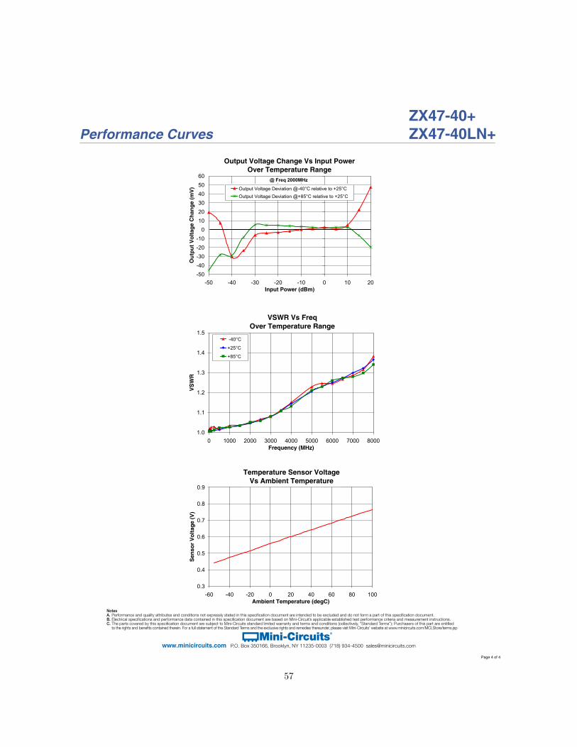
NotesA. Performance and quality attributes and conditions not expressly stated in this specification document are intended to be excluded and do not form a part of this specification document. B. Electrical specifications and performance data contained in this specification document are based on Mini-Circuit’s applicable established test performance criteria and measurement instructions. C. The parts covered by this specification document are subject to Mini-Circuits standard limited warranty and terms and conditions (collectively, “Standard Terms”); Purchasers of this part are entitled to the rights and benefits contained therein. For a full statement of the Standard Terms and the exclusive rights and remedies thereunder, please visit Mini-Circuits’ website at www.minicircuits.com/MCLStore/terms.jsp
Mini-Circuits®
www.minicircuits.com P.O. Box 350166, Brooklyn, NY 11235-0003 (718) 934-4500 [email protected]
Page 4 of 4
Performance CurvesZX47-40+ZX47-40LN+
VSWR Vs FreqOver Temperature Range
1.0
1.1
1.2
1.3
1.4
1.5
0 1000 2000 3000 4000 5000 6000 7000 8000Frequency (MHz)
VS
WR
-40°C
+25°C
+85°C
Temperature Sensor VoltageVs Ambient Temperature
0.3
0.4
0.5
0.6
0.7
0.8
0.9
-60 -40 -20 0 20 40 60 80 100Ambient Temperature (degC)
Sen
sor
Vol
tage
(V)
Output Voltage Change Vs Input PowerOver Temperature Range
-50-40-30-20-10
0102030405060
-50 -40 -30 -20 -10 0 10 20Input Power (dBm)
Out
put V
olta
ge C
hang
e (m
V) Output Voltage Deviation @-40°C relative to +25°C
Output Voltage Deviation @+85°C relative to +25°C
@ Freq 2000MHz
57
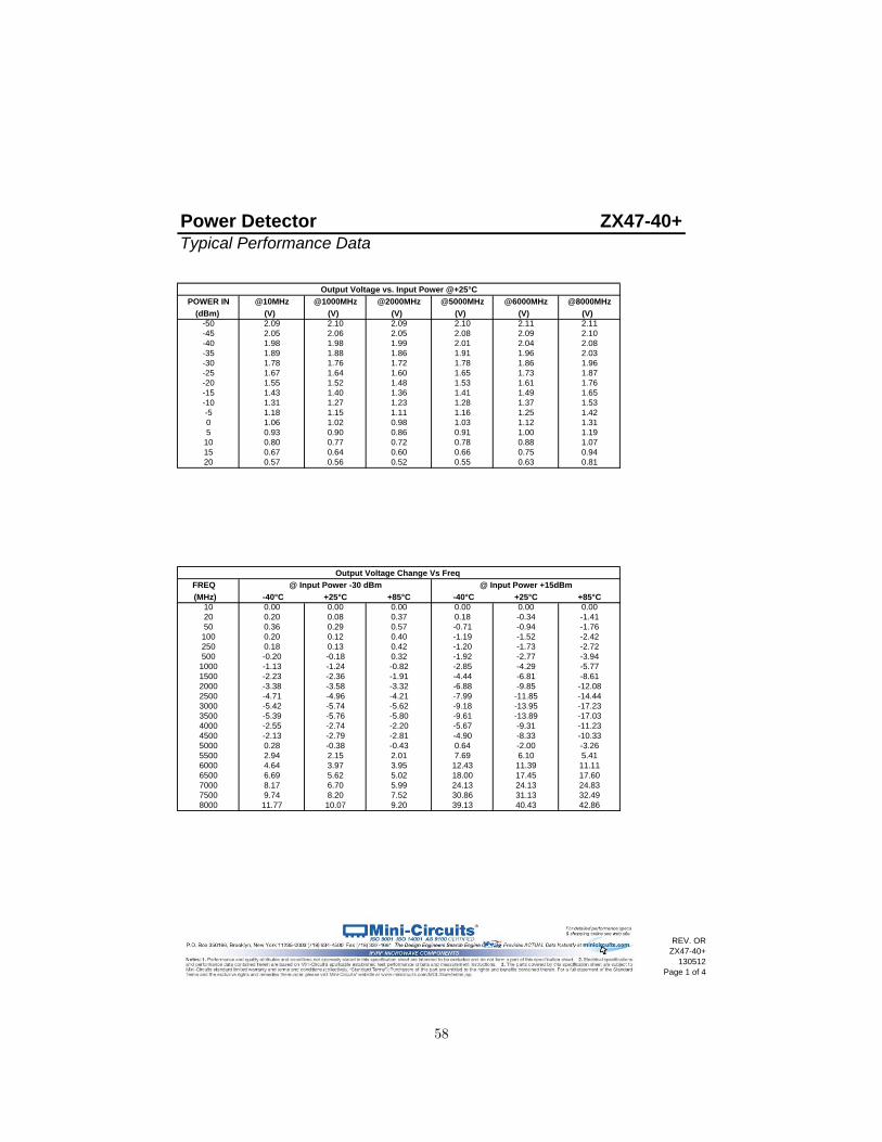
Power DetectorTypical Performance Data
POWER IN @1000MHz @5000MHz @8000MHz (dBm) (V) (V) (V)
-50 2.10 2.10 2.11-45 2.06 2.08 2.10-40 1.98 2.01 2.08-35 1.88 1.91 2.03-30 1.76 1.78 1.96-25 1.64 1.65 1.87-20 1.52 1.53 1.76-15 1.40 1.41 1.65-10 1.27 1.28 1.53-5 1.15 1.16 1.420 1.02 1.03 1.315 0.90 0.91 1.19
10 0.77 0.78 1.0715 0.64 0.66 0.9420 0.56 0.55 0.81
FREQ (MHz) +25°C -40°C +85°C
10 0.00 0.00 0.0020 0.08 0.18 -1.4150 0.29 -0.71 -1.76100 0.12 -1.19 -2.42250 0.13 -1.20 -2.72500 -0.18 -1.92 -3.94
1000 -1.24 -2.85 -5.771500 -2.36 -4.44 -8.612000 -3.58 -6.88 -12.082500 -4.96 -7.99 -14.443000 -5.74 -9.18 -17.233500 -5.76 -9.61 -17.034000 -2.74 -5.67 -11.234500 -2.79 -4.90 -10.335000 -0.38 0.64 -3.265500 2.15 7.69 5.416000 3.97 12.43 11.116500 5.62 18.00 17.607000 6.70 24.13 24.837500 8.20 30.86 32.498000 10.07 39.13 42.86
0.600.52
ZX47-40+
1.251.121.000.88
Output Voltage vs. Input Power @+25°C
2.112.092.041.96
0.750.63
0.860.72
1.861.731.611.49
1.601.481.361.231.110.98
24.1331.1340.43
2.092.051.981.891.781.671.55
-9.31-8.33-2.006.10
11.3917.45
-4.29-6.81-9.85
-11.85-13.95-13.89
+25°C -40°C0.000.20
0.000.37
0.00-0.34
+85°C
0.360.200.18
0.570.400.42
@6000MHz (V)
@10MHz (V) (V)
@2000MHz
-4.71-5.42
-0.94-1.52-1.73-2.77-0.20
-1.130.32-0.82
-2.55
1.311.181.06
0.57
0.930.800.67
-2.23-3.38
1.43
0.282.94
-1.91-3.32-4.21-5.62-5.80-2.20
-5.39
-2.13
@ Input Power +15dBmOutput Voltage Change Vs Freq
@ Input Power -30 dBm
2.092.051.991.861.72
1.37
-2.81-0.432.013.955.025.99
9.7411.77
7.529.20
4.646.698.17
REV. ORZX47-40+
130512Page 1 of 4
58
Power DetectorTypical Performance Data
Measured Output Voltage(V) Ideal Deviation
from ideaOutput Voltage
(V) Ideal Deviation from idea
-50 2.09 -43.56 -6.44 2.09 -44.03 -5.97-45 2.05 -42.00 -3.00 2.05 -42.34 -2.66-40 1.98 -39.00 -1.00 1.99 -40.00 0.00-35 1.89 -35.00 0.00 1.86 -34.94 -0.06-30 1.78 -30.67 0.67 1.72 -29.52 -0.48-25 1.67 -25.65 0.65 1.60 -24.68 -0.32-20 1.55 -20.77 0.77 1.48 -20.00 0.00-15 1.43 -15.70 0.70 1.36 -15.21 0.21-10 1.31 -10.59 0.59 1.23 -10.35 0.35-5 1.18 -5.29 0.29 1.11 -5.51 0.510 1.06 0.00 0.00 0.98 -0.67 0.675 0.93 5.40 -0.40 0.86 4.32 0.68
10 0.80 10.95 -0.95 0.72 9.52 0.4815 0.67 16.23 -1.23 0.60 14.21 0.7920 0.57 20.36 -0.36 0.52 17.49 2.51
Measured Output Voltage (V) Ideal Deviation
from ideaOutput Voltage
(V) Ideal Deviation from idea
-50 2.11 -41.01 -8.99 2.11 -36.79 -13.42-45 2.09 -40.34 -4.66 2.10 -36.47 -8.73-40 2.04 -38.29 -1.71 2.08 -35.22 -4.95-35 1.96 -35.00 0.00 2.03 -33.26 -1.84-30 1.86 -30.41 0.41 1.96 -30.00 0.00-25 1.73 -25.33 0.33 1.87 -25.53 0.67-20 1.61 -20.19 0.19 1.76 -20.57 0.87-15 1.49 -15.00 0.00 1.65 -15.31 0.78-10 1.37 -9.73 -0.27 1.53 -10.00 0.64-5 1.25 -4.63 -0.37 1.42 -4.83 0.640 1.12 0.51 -0.51 1.31 0.34 0.635 1.00 5.80 -0.80 1.19 5.67 0.47
10 0.88 10.97 -0.97 1.07 11.32 0.0015 0.75 16.41 -1.41 0.94 17.25 -0.7420 0.63 21.53 -1.53 0.81 23.40 -1.70
@6000MHz(mV/dB) @8000MHz(mV/dB)
ZX47-40+
Sensitivity vs. Input Power @+25°C
Sensitivity vs. Input Power @+25°C
@10MHz(mV/dB) @2000MHz(mV/dB)
REV. ORZX47-40+
130512Page 2 of 4
59
Power Detector ZX47-40+Typical Performance Data
POWER IN (dBm)
-40°C +25°C +85°C -40°C +25°C +85°C -40°C +25°C +85°C-50 -9.08 -7.42 -2.62 -5.82 -4.74 -3.26 -1.54 -1.38 0.06-45 -15.94 -14.24 -10.16 -14.90 -13.32 -7.08 -4.36 -5.44 -1.58-40 -20.56 -19.00 -17.10 -23.16 -21.46 -19.06 -9.68 -8.44 -7.08-35 -21.66 -20.58 -20.94 -25.76 -25.48 -24.62 -15.54 -14.12 -12.32-30 -23.38 -23.82 -22.54 -25.20 -25.06 -24.78 -20.36 -19.34 -17.30-25 -23.32 -23.16 -22.58 -24.54 -24.72 -24.46 -22.28 -21.46 -20.06-20 -23.80 -24.10 -24.32 -24.98 -24.70 -24.28 -23.78 -22.74 -21.06-15 -24.80 -24.24 -24.78 -24.76 -25.04 -25.10 -23.86 -22.96 -21.56-10 -24.70 -25.20 -25.08 -24.76 -24.92 -24.62 -23.08 -22.34 -21.32-5 -24.68 -25.10 -25.02 -24.34 -24.34 -24.42 -22.90 -22.36 -21.620 -25.72 -25.64 -25.74 -24.58 -25.06 -25.06 -23.56 -23.08 -22.645 -26.14 -26.36 -26.22 -25.06 -25.06 -24.92 -24.24 -24.42 -24.3010 -23.68 -25.06 -24.64 -22.12 -25.10 -26.20 -25.22 -25.64 -25.5615 -15.82 -19.60 -20.96 -17.32 -20.88 -23.02 -23.32 -26.62 -29.00
FREQ (MHz)
-40°C +25°C +85°C -40°C +25°C +85°C -40°C +25°C +85°C10 -20.56 -19.00 -17.10 -23.32 -23.16 -22.58 -25.72 -25.64 -25.74
250 -21.18 -19.62 -17.28 -24.16 -24.60 -23.76 -25.54 -25.52 -25.58500 -21.90 -20.90 -17.72 -24.20 -24.30 -24.64 -25.52 -25.50 -25.521000 -22.62 -20.94 -18.78 -23.82 -24.10 -24.32 -25.18 -25.28 -25.441500 -23.94 -22.20 -19.78 -24.12 -24.22 -24.44 -25.42 -25.02 -25.082000 -24.38 -25.82 -21.70 -23.74 -23.90 -23.98 -25.90 -25.50 -25.382500 -24.28 -23.38 -23.72 -23.64 -24.04 -22.66 -25.72 -25.46 -25.503000 -23.54 -23.30 -23.22 -23.88 -24.12 -24.20 -25.84 -25.48 -25.463500 -27.02 -27.94 -27.32 -23.96 -23.82 -23.60 -25.78 -25.42 -25.444000 -21.30 -19.74 -18.82 -24.60 -25.34 -25.82 -24.86 -25.14 -25.404500 -23.66 -23.14 -21.70 -24.84 -24.70 -24.48 -24.68 -25.00 -25.225000 -23.16 -21.46 -19.06 -24.54 -24.72 -24.46 -24.58 -25.06 -25.065500 -20.22 -17.90 -15.60 -24.08 -23.84 -23.46 -24.94 -25.04 -24.626000 -17.98 -15.56 -13.06 -24.38 -24.32 -24.14 -25.00 -25.06 -24.466500 -15.68 -13.76 -11.70 -24.72 -24.38 -23.54 -24.68 -24.48 -23.787000 -13.66 -12.44 -10.44 -23.84 -23.10 -22.16 -24.32 -23.80 -23.007500 -12.14 -10.80 -8.90 -23.00 -22.30 -21.22 -23.96 -23.68 -23.268000 -9.68 -8.44 -7.08 -22.28 -21.46 -20.06 -23.56 -23.08 -22.64
Slope Vs Input Power Over TemperatureRange @ Freq 10MHz Range @ Freq 5000MHz Range @ Freq 8000MHz
Slope Vs Freq Over Temperature Range @ Input Power -40dBm @ Input Power -25dBm @ Input Power 0dBm
REV. ORZX47-40+
130512Page 3 of 4
60
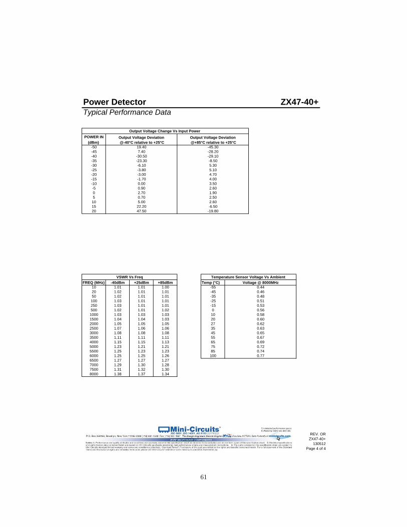
Power DetectorTypical Performance Data
POWER IN (dBm)
-50 19.40 -45.30-45 7.40 -28.20-40 -30.50 -29.10-35 -23.30 -8.50-30 -6.10 5.30-25 -3.80 5.10-20 -3.00 4.70-15 -1.70 4.00-10 0.00 3.50-5 0.90 2.600 2.70 1.905 0.70 2.5010 5.00 2.6015 22.20 -6.5020 47.50 -19.80
FREQ (MHz) -40dBm +25dBm +85dBm Temp (°C) 10 1.01 1.01 1.00 -55 0.4420 1.02 1.01 1.01 -45 0.4650 1.02 1.01 1.01 -35 0.48
100 1.03 1.01 1.01 -25 0.51250 1.03 1.01 1.01 -15 0.53500 1.02 1.01 1.02 0 0.561000 1.03 1.03 1.03 10 0.581500 1.04 1.04 1.03 20 0.602000 1.05 1.05 1.05 27 0.622500 1.07 1.06 1.06 35 0.633000 1.08 1.08 1.08 45 0.653500 1.11 1.11 1.11 55 0.674000 1.15 1.15 1.13 65 0.695000 1.23 1.21 1.21 75 0.725500 1.25 1.23 1.23 85 0.746000 1.25 1.25 1.26 100 0.776500 1.27 1.27 1.277000 1.29 1.30 1.287500 1.31 1.32 1.308000 1.38 1.37 1.34
ZX47-40+
Voltage @ 8000MHzTemperature Sensor Voltage Vs Ambient
Output Voltage Change Vs Input Power
VSWR Vs Freq
Output Voltage Deviation @-40°C relative to +25°C
Output Voltage Deviation @+85°C relative to +25°C
REV. ORZX47-40+
130512Page 4 of 4
61
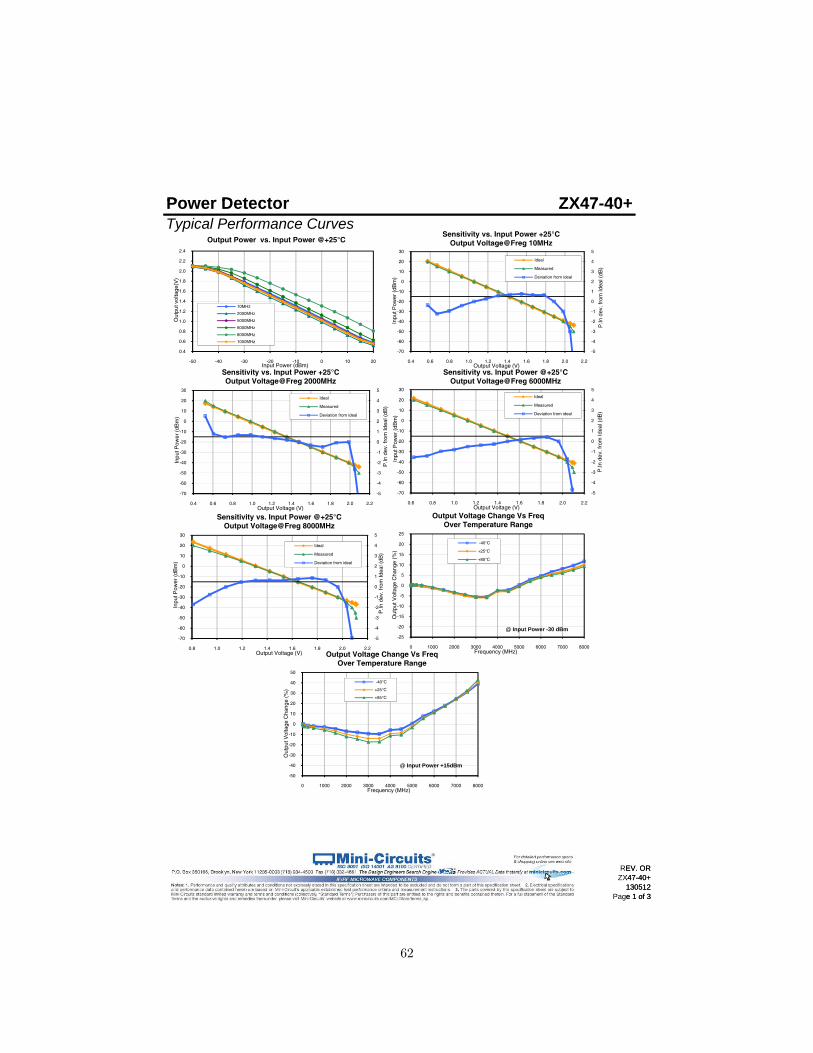
Power Detector ZX47 40+
REV. ORZX47-40+
130512Page 1 of 3
Power DetectorTypical Performance Curves
ZX47-40+
1.6
1.8
2.0
2.2
2.4
tage
(V)
Output Power vs. Input Power @+25°C
1
2
3
4
5
-10
0
10
20
30
r (d
Bm
)
Sensitivity vs. Input Power +25°COutput Voltage@Freg 10MHz
Ideal
Measured
Deviation from ideal
m Id
eal (
dB)
0.4
0.6
0.8
1.0
1.2
1.4
-50 -40 -30 -20 -10 0 10 20
Out
put v
olt
Input Power (dBm)
10MHz
2000MHz
5000MHz
6000MHz
8000MHz
1000MHz
-5
-4
-3
-2
-1
0
-70
-60
-50
-40
-30
-20
0.4 0.6 0.8 1.0 1.2 1.4 1.6 1.8 2.0 2.2
Inpu
t Pow
er
Output Voltage (V)
P.In
dev
. fro
m
530
Sensitivity vs. Input Power +25°COutput Voltage@Freg 2000MHz
530
Sensitivity vs. Input Power @+25°COutput Voltage@Freg 6000MHz
-4
-3
-2
-1
0
1
2
3
4
5
-60
-50
-40
-30
-20
-10
0
10
20
30
Inpu
t Pow
er (
dBm
)
Ideal
Measured
Deviation from ideal
P.In
dev
. fro
m Id
eal (
dB)
-4
-3
-2
-1
0
1
2
3
4
5
-60
-50
-40
-30
-20
-10
0
10
20
30In
put P
ower
(dB
m)
Ideal
Measured
Deviation from ideal
P.In
dev
. fro
m Id
eal (
dB)
-5-70
0.4 0.6 0.8 1.0 1.2 1.4 1.6 1.8 2.0 2.2Output Voltage (V)
-5-70
0.6 0.8 1.0 1.2 1.4 1.6 1.8 2.0 2.2Output Voltage (V)
1
2
3
4
5
-10
0
10
20
30
er (
dBm
)
Sensitivity vs. Input Power @+25°COutput Voltage@Freg 8000MHz
Ideal
Measured
Deviation from ideal
m Id
eal (
dB)
5
10
15
20
25
Cha
nge
(%)
Output Voltage Change Vs Freq Over Temperature Range
-40°C
+25°C
+85°C
-5
-4
-3
-2
-1
0
-70
-60
-50
-40
-30
-20
0.8 1.0 1.2 1.4 1.6 1.8 2.0 2.2
Inpu
t Pow
e
Output Voltage (V)
P.In
dev
. fro
m
-25
-20
-15
-10
-5
0
0 1000 2000 3000 4000 5000 6000 7000 8000
Out
put V
olta
ge
Frequency (MHz)
@ Input Power -30 dBm
50
Output Voltage Change Vs Freq Over Temperature Range
-40
-30
-20
-10
0
10
20
30
40
Out
put V
olta
ge C
hang
e (%
)
-40°C
+25°C
+85°C
@ Input Power +15dBm
-50
0 1000 2000 3000 4000 5000 6000 7000 8000Frequency (MHz)
REV. ORZX47-40+
130512Page 1 of 3
62
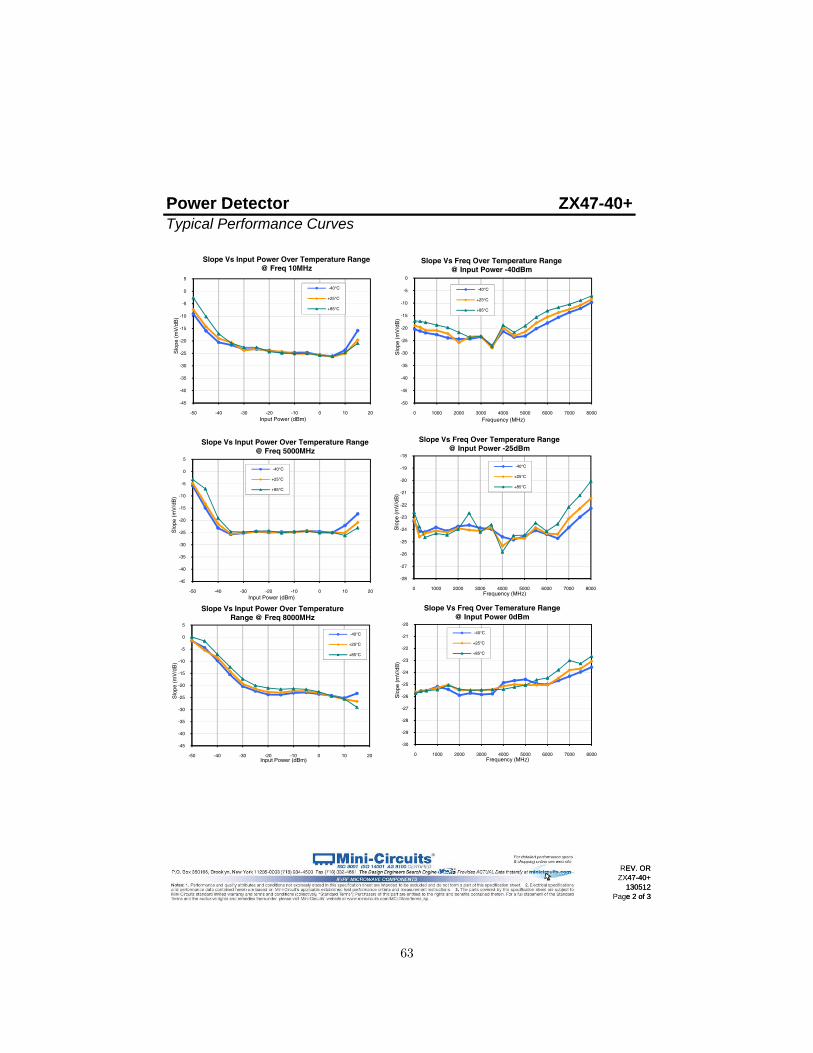
Power Detector ZX47 40+
REV. ORZX47-40+
130512Page 2 of 3
Power DetectorTypical Performance Curves
ZX47-40+
0
5
Slope Vs Input Power Over Temperature Range @ Freq 10MHz
-40°C -5
0
Slope Vs Freq Over Temperature Range@ Input Power -40dBm
-40°C
-40
-35
-30
-25
-20
-15
-10
-5
Slo
pe (
mV
/dB
)
+25°C
+85°C
-45
-40
-35
-30
-25
-20
-15
-10
Slo
pe (
mV
/dB
)
+25°C
+85°C
-45
-40
-50 -40 -30 -20 -10 0 10 20Input Power (dBm)
-50
-45
0 1000 2000 3000 4000 5000 6000 7000 8000
Frequency (MHz)
-5
0
5
Slope Vs Input Power Over Temperature Range @ Freq 5000MHz
-40°C
+25°C -20
-19
-18
Slope Vs Freq Over Temperature Range@ Input Power -25dBm
-40°C
+25°C
85°C
45
-40
-35
-30
-25
-20
-15
-10
Slo
pe (
mV
/dB
)
+85°C
-28
-27
-26
-25
-24
-23
-22
-21
Slo
pe (
mV
/dB
)
+85°C
-45
-50 -40 -30 -20 -10 0 10 20Input Power (dBm)
-15
-10
-5
0
5
V/d
B)
Slope Vs Input Power Over TemperatureRange @ Freq 8000MHz
-40°C
+25°C
+85°C
-24
-23
-22
-21
-20
mV
/dB
)
Slope Vs Freq Over Temerature Range @ Input Power 0dBm
-40°C
+25°C
+85°C
0 1000 2000 3000 4000 5000 6000 7000 8000Frequency (MHz)
-45
-40
-35
-30
-25
-20
-50 -40 -30 -20 -10 0 10 20
Slo
pe (
mV
Input Power (dBm)
-30
-29
-28
-27
-26
-25
0 1000 2000 3000 4000 5000 6000 7000 8000
Slo
pe (
m
Frequency (MHz)
REV. ORZX47-40+
130512Page 2 of 3
63
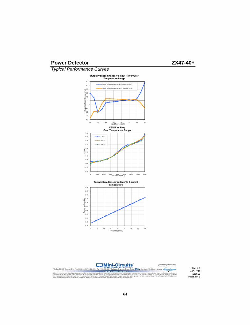
Power Detector ZX47 40+
REV. ORZX47-40+
130512Page 3 of 3
Power DetectorTypical Performance Curves
ZX47-40+
30
40
50
V)
Output Voltage Change Vs Input Power Over Temperature Range
Output Voltage Deviation @-40°C relative to +25°C
Output Voltage Deviation @+85°C relative to +25°C
-50
-40
-30
-20
-10
0
10
20
Out
put V
olta
ge C
hang
e (m
-50 -40 -30 -20 -10 0 10 20Input Power (dBm)
1.20
1.25
1.30
1.35
1.40
WR
VSWR Vs FreqOver Temperature Range
-40°C
+25°C
+85°C
0.90
0.95
1.00
1.05
1.10
1.15
0 1000 2000 3000 4000 5000 6000 7000 8000
VS
W
Frequency (MHz)
0.65
0.70
0.75
0.80
0.85
0.90
or V
olta
ge (
V)
Temperature Sensor Voltage Vs Ambient Temperature
0.40
0.45
0.50
0.55
0.60
-60 -40 -20 0 20 40 60 80 100
Sen
so
Frequency (MHz)
REV. ORZX47-40+
130512Page 3 of 3
64
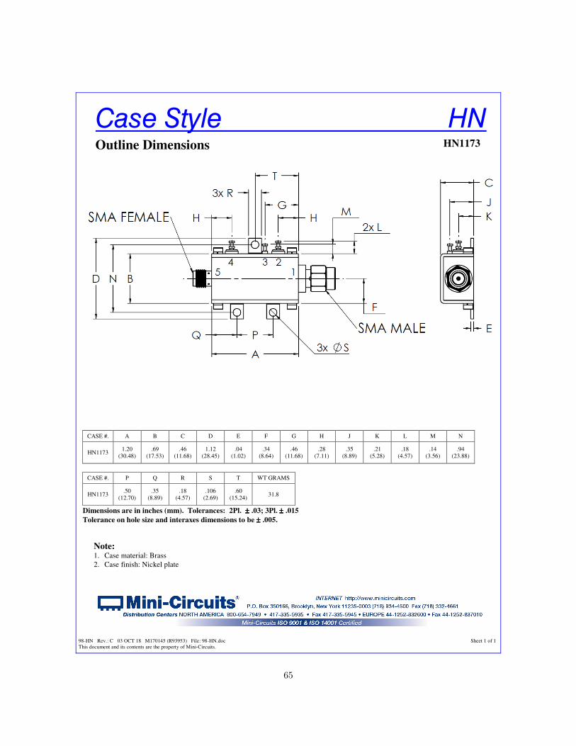
Case Style HN
98-HN Rev.: C 03 OCT 18 M170145 (R93953) File: 98-HN.doc Sheet 1 of 1
This document and its contents are the property of Mini-Circuits.
Outline Dimensions
HN1173
CASE #. A B C D E F G H J K L M N
HN1173 1.20
(30.48)
.69
(17.53)
.46
(11.68)
1.12
(28.45)
.04
(1.02)
.34
(8.64)
.46
(11.68)
.28
(7.11)
.35
(8.89)
.21
(5.28)
.18
(4.57)
.14
(3.56)
.94
(23.88)
CASE #. P Q R S T WT GRAMS
HN1173 .50
(12.70)
.35
(8.89)
.18
(4.57)
.106
(2.69)
.60
(15.24) 31.8
Dimensions are in inches (mm). Tolerances: 2Pl. ±±±± .03; 3Pl. ±±±± .015
Tolerance on hole size and interaxes dimensions to be ±±±± .005.
Note: 1. Case material: Brass
2. Case finish: Nickel plate
65
Mini-Circuits Environmental Specifications
All Mini-Circuits products are manufactured under exacting quality assurance and control standards, and are capable of meeting published specifications after being subjected to any or all of the following physical and environmental test.
Specification Test/Inspection Condition Reference/Spec
ENV28T5
Operating Temperature -40° to 85°C Individual Model Data Sheet
Storage Temperature -55° to 100° CAmbient Environment
Individual Model Data Sheet
Barometric Pressure 100,000 Feet MIL-STD-202, Method 105, Condition D
Humidity 90% RH, 65°CUnits may require bake-out after humidity to restore full performance.
MIL-STD-202, Method 103
Thermal Shock -65° to 125°C, 5 cycles MIL-STD-202, Method 107, Condition B
Vibration (High Frequency) 20g peak, 10-2000 Hz, 12 times in each of three perpendicular directions (total 36)
MIL-STD-202, Method 204, Condition D
Mechanical Shock 100g, 6ms sawtooth, 3 shocks each direction 3 axes (total 18)
MIL-STD-202, Method 213, Condition I
This document and its contents are the property of Mini-Circuits.
Rev:ENV28T5 A 09/26/13 File:M143494 ENV28T5.pdfPage: 1
66

Appendix B.2: 1N5817 Diode
67
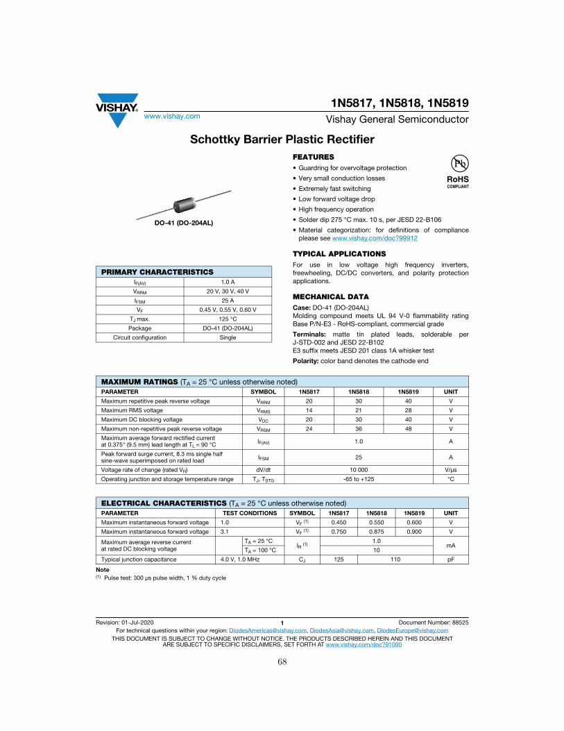
1N5817, 1N5818, 1N5819www.vishay.com Vishay General Semiconductor
Revision: 01-Jul-2020 1 Document Number: 88525For technical questions within your region: [email protected], [email protected], [email protected]
THIS DOCUMENT IS SUBJECT TO CHANGE WITHOUT NOTICE. THE PRODUCTS DESCRIBED HEREIN AND THIS DOCUMENTARE SUBJECT TO SPECIFIC DISCLAIMERS, SET FORTH AT www.vishay.com/doc?91000
Schottky Barrier Plastic RectifierFEATURES• Guardring for overvoltage protection
• Very small conduction losses
• Extremely fast switching
• Low forward voltage drop
• High frequency operation
• Solder dip 275 °C max. 10 s, per JESD 22-B106
• Material categorization: for definitions of compliance please see www.vishay.com/doc?99912
TYPICAL APPLICATIONSFor use in low voltage high frequency inverters, freewheeling, DC/DC converters, and polarity protection applications.
MECHANICAL DATACase: DO-41 (DO-204AL)Molding compound meets UL 94 V-0 flammability rating Base P/N-E3 - RoHS-compliant, commercial grade
Terminals: matte tin plated leads, solderable per J-STD-002 and JESD 22-B102E3 suffix meets JESD 201 class 1A whisker test
Polarity: color band denotes the cathode end
Note(1) Pulse test: 300 μs pulse width, 1 % duty cycle
PRIMARY CHARACTERISTICSIF(AV) 1.0 A
VRRM 20 V, 30 V, 40 V
IFSM 25 A
VF 0.45 V, 0.55 V, 0.60 V
TJ max. 125 °C
Package DO-41 (DO-204AL)
Circuit configuration Single
DO-41 (DO-204AL)
MAXIMUM RATINGS (TA = 25 °C unless otherwise noted)PARAMETER SYMBOL 1N5817 1N5818 1N5819 UNIT
Maximum repetitive peak reverse voltage VRRM 20 30 40 V
Maximum RMS voltage VRMS 14 21 28 V
Maximum DC blocking voltage VDC 20 30 40 V
Maximum non-repetitive peak reverse voltage VRSM 24 36 48 V
Maximum average forward rectified currentat 0.375" (9.5 mm) lead length at TL = 90 °C IF(AV) 1.0 A
Peak forward surge current, 8.3 ms single halfsine-wave superimposed on rated load IFSM 25 A
Voltage rate of change (rated VR) dV/dt 10 000 V/μs
Operating junction and storage temperature range TJ, TSTG -65 to +125 °C
ELECTRICAL CHARACTERISTICS (TA = 25 °C unless otherwise noted)PARAMETER TEST CONDITIONS SYMBOL 1N5817 1N5818 1N5819 UNIT
Maximum instantaneous forward voltage 1.0 VF (1) 0.450 0.550 0.600 V
Maximum instantaneous forward voltage 3.1 VF (1) 0.750 0.875 0.900 V
Maximum average reverse currentat rated DC blocking voltage
TA = 25 °CIR (1)
1.0mA
TA = 100 °C 10
Typical junction capacitance 4.0 V, 1.0 MHz CJ 125 110 pF
68
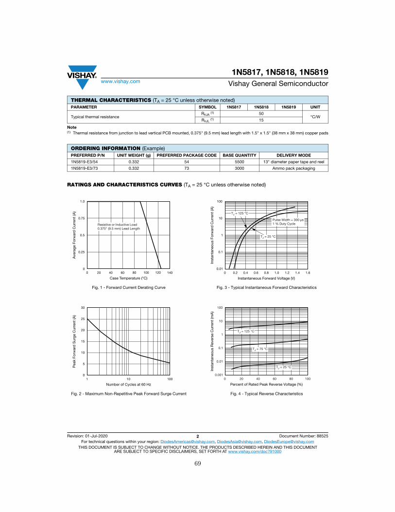
1N5817, 1N5818, 1N5819www.vishay.com Vishay General Semiconductor
Revision: 01-Jul-2020 2 Document Number: 88525For technical questions within your region: [email protected], [email protected], [email protected]
THIS DOCUMENT IS SUBJECT TO CHANGE WITHOUT NOTICE. THE PRODUCTS DESCRIBED HEREIN AND THIS DOCUMENTARE SUBJECT TO SPECIFIC DISCLAIMERS, SET FORTH AT www.vishay.com/doc?91000
Note(1) Thermal resistance from junction to lead vertical PCB mounted, 0.375" (9.5 mm) lead length with 1.5" x 1.5" (38 mm x 38 mm) copper pads
RATINGS AND CHARACTERISTICS CURVES (TA = 25 °C unless otherwise noted)
Fig. 1 - Forward Current Derating Curve
Fig. 2 - Maximum Non-Repetitive Peak Forward Surge Current
Fig. 3 - Typical Instantaneous Forward Characteristics
Fig. 4 - Typical Reverse Characteristics
THERMAL CHARACTERISTICS (TA = 25 °C unless otherwise noted)PARAMETER SYMBOL 1N5817 1N5818 1N5819 UNIT
Typical thermal resistanceRJA (1) 50
°C/WRJL (1) 15
ORDERING INFORMATION (Example)PREFERRED P/N UNIT WEIGHT (g) PREFERRED PACKAGE CODE BASE QUANTITY DELIVERY MODE
1N5819-E3/54 0.332 54 5500 13" diameter paper tape and reel
1N5819-E3/73 0.332 73 3000 Ammo pack packaging
0
0.25
0.5
0.75
0 40 6020 80 100 120 140
1.0
Ave
rage
For
war
d C
urre
nt (A
)
Case Temperature (°C)
Resistive or Inductive Load0.375" (9.5 mm) Lead Length
1 10 1000
5
10
15
20
25
30
Number of Cycles at 60 Hz
Pea
k Fo
rwar
d S
urge
Cur
rent
(A)
Inst
anta
neou
s Fo
rwar
d C
urre
nt (A
)
100
10
1
0.1
0.01
Instantaneous Forward Voltage (V)
0 0.40.2 1.20.80.6 1.4 1.61.0
TJ = 125 °C
TJ = 25 °C
Pulse Width = 300 μs1 % Duty Cycle
Inst
anta
neou
s R
ever
se C
urre
nt (m
A)
1
10
100
0.01
0.001
0.1
200 10040 60 80
Percent of Rated Peak Reverse Voltage (%)
TJ = 125 °C
TJ = 25 °C
TJ = 75 °C
69
1N5817, 1N5818, 1N5819www.vishay.com Vishay General Semiconductor
Revision: 01-Jul-2020 3 Document Number: 88525For technical questions within your region: [email protected], [email protected], [email protected]
THIS DOCUMENT IS SUBJECT TO CHANGE WITHOUT NOTICE. THE PRODUCTS DESCRIBED HEREIN AND THIS DOCUMENTARE SUBJECT TO SPECIFIC DISCLAIMERS, SET FORTH AT www.vishay.com/doc?91000
Fig. 5 - Typical Junction Capacitance
Fig. 6 - Typical Junction Capacitance
Fig. 7 - Typical Transient Thermal Impedance
PACKAGE OUTLINE DIMENSIONS in inches (millimeters)
Junc
tion
Cap
acita
nce
(pF)
101 100
100
1000
100.1
Reverse Voltage (V)
1N5817
TJ = 25 °Cf = 1.0 MHzVsig = 50 mVp-p
Junc
tion
Cap
acita
nce
(pF)
101 100
100
1000
100.1
Reverse Voltage (V)
1N5818, 1N5819
TJ = 25 °Cf = 1.0 MHzVsig = 50 mVp-p
0.01 101 100
10
100
0.10.1
1
t - Pulse Duration (s)
Tran
sien
t Th
erm
al Im
ped
ance
(°C
/W)
DO-41 (DO-204AL)
0.107 (2.7)0.080 (2.0)
DIA.
0.034 (0.86)0.028 (0.71)
DIA.
1.0 (25.4)MIN.
1.0 (25.4)MIN.
0.205 (5.2)0.160 (4.1)
70
Legal Disclaimer Noticewww.vishay.com Vishay
Revision: 01-Jan-2021 1 Document Number: 91000
Disclaimer ALL PRODUCT, PRODUCT SPECIFICATIONS AND DATA ARE SUBJECT TO CHANGE WITHOUT NOTICE TO IMPROVE RELIABILITY, FUNCTION OR DESIGN OR OTHERWISE.
Vishay Intertechnology, Inc., its affiliates, agents, and employees, and all persons acting on its or their behalf (collectively, “Vishay”), disclaim any and all liability for any errors, inaccuracies or incompleteness contained in any datasheet or in any other disclosure relating to any product.
Vishay makes no warranty, representation or guarantee regarding the suitability of the products for any particular purpose or the continuing production of any product. To the maximum extent permitted by applicable law, Vishay disclaims (i) any and all liability arising out of the application or use of any product, (ii) any and all liability, including without limitation special, consequential or incidental damages, and (iii) any and all implied warranties, including warranties of fitness for particular purpose, non-infringement and merchantability.
Statements regarding the suitability of products for certain types of applications are based on Vishay’s knowledge of typical requirements that are often placed on Vishay products in generic applications. Such statements are not binding statements about the suitability of products for a particular application. It is the customer’s responsibility to validate that a particular product with the properties described in the product specification is suitable for use in a particular application. Parameters provided in datasheets and / or specifications may vary in different applications and performance may vary over time. All operating parameters, including typical parameters, must be validated for each customer application by the customer’s technical experts. Product specifications do not expand or otherwise modify Vishay’s terms and conditions of purchase, including but not limited to the warranty expressed therein.
Except as expressly indicated in writing, Vishay products are not designed for use in medical, life-saving, or life-sustaining applications or for any other application in which the failure of the Vishay product could result in personal injury or death. Customers using or selling Vishay products not expressly indicated for use in such applications do so at their own risk. Please contact authorized Vishay personnel to obtain written terms and conditions regarding products designed for such applications.
No license, express or implied, by estoppel or otherwise, to any intellectual property rights is granted by this document or by any conduct of Vishay. Product names and markings noted herein may be trademarks of their respective owners.
© 2021 VISHAY INTERTECHNOLOGY, INC. ALL RIGHTS RESERVED
71


![Improved Split-Ring Resonator for Microfluidicorca.cf.ac.uk/59763/1/Improved split ring.pdf · 2020. 11. 26. · The resonant frequency of a cavity resonator [13] is set by its dimensions,](https://img.pdfslide.us/doc/110x75/60f99d8762b1d658425e30d9/improved-split-ring-resonator-for-split-ringpdf-2020-11-26-the-resonant.jpg)