Embed Size (px)
Citation preview

1 21
Winstar Display Co., LTD : 407 163 No.163 Chung Ching RD., Taichune, Taiwan, R.O.C
WEB: http://www.winstar.com.tw E-mail: [email protected] Tel:886-4-24262208 Fax 886-4-24262207
SPECIFICATION
CUSTOMER : MODULE NO.: WH1602A-YGH-CTK
APPROVED BY: ( FOR CUSTOMER USE ONLY )
SALES BY APPROVED BY CHECKED BY PREPARED BY
ISSUED DATE:

2 21
Winstar Display Co., LTD
MODLE NO
RECORDS OF REVISION DOC. FIRST ISSUE
VERSION DATE
REVISED PAGE NO. SUMMARY
0 2004.07.30 First issue

3 21
Contents 1.Module Classification Information
2.Precautions in use of LCD Modules
3.General Specification
4.Absolute Maximum Ratings
5.Electrical Characteristics
6.Optical Characteristics
7.Interface Pin Function
8.Contour Drawing & Block Diagram
9.Function Description
10.Character Generator ROM Pattern
11.Instruction Table
12.Timing Characteristics
13.Initializing of LCM
14.Quality Assurance
15.Reliability
16.Backlight Information

4 21
1.Module Classification Information W H 1 6 0 2 A Y G H CTK Å Ç É Ñ Ö Ü á à Å Brand WINSTAR DISPLAY CORPORATION Ç Display Type H→Character Type, G→Graphic Type É Display Font Character 16 words, 2Lines. Ñ Model serials no. Ö Backlight Type N→Without backlight
B→EL, Blue green D→EL, Green W→EL, White F→CCFL, White Y→LED, Yellow Green
A→LED, Amber R→LED, Red O→LED, Orange G→LED, Green
Ü LCD Mode B→TN Positive, Gray T→FSTN Negative N→TN Negative, G→STN Positive, Gray Y→STN Positive, Yellow Green M→STN Negative, Blue F→FSTN Positive
á LCD Polarize Type/ Temperature range/ View direction
A→Reflective, N.T, 6:00 D→Reflective, N.T, 12:00 G→Reflective, W. T, 6:00 J→Reflective, W. T, 12:00 B→Transflective, N.T,6:00 E→Transflective, N.T.12:00
H→Transflective, W.T,6:00 K→Transflective, W.T,12:00 C→Transmissive, N.T,6:00 F→Transmissive, N.T,12:00 I→Transmissive, W. T, 6:00 L→Transmissive, W.T,12:00
à Special Code CT : English and Cyrillic standard font ;K: LED 20 DICE
2.Precautions in use of LCD Modules

5 21
(1)Avoid applying excessive shocks to the module or making any alterations or modifications to it.
(2)Don’t make extra holes on the printed circuit board, modify its shape or change the components of LCD module.
(3)Don’t disassemble the LCM. (4)Don’t operate it above the absolute maximum rating. (5)Don’t drop, bend or twist LCM. (6)Soldering: only to the I/O terminals. (7)Storage: please storage in anti-static electricity container and clean environment.
3.General Specification Item Dimension Unit
Number of Characters 16 characters x 2 Lines Module dimension 84.0 x 44.0 x 13.5(MAX) mm View area 66.0 x 16.0 mm Active area 56.20 x 11.5 mm Dot size 0.55 x 0.65 mm Dot pitch 0.60 x 0.70 mm Character size 2.95 x 5.55 mm Character pitch 3.55 x 5.95 mm LCD type STN, Positive, Transflective, Gray Duty 1/16 View direction 6 o’clock Backlight Type LED Yellow green
4.Absolute Maximum Ratings

6 21
Item Symbol Min Typ Max Unit Operating Temperature TOP -20 +70 Storage Temperature TST -30 +80 Input Voltage VI VSS VDD V Supply Voltage For Logic VDD-VSS -0.3 7 V Supply Voltage For LCD VDD-V0 -0.3 13 V
5.Electrical Characteristics Item Symbol Condition Min Typ Max Unit
Supply Voltage For Logic VDD-VSS 4.5 5.5 V
Supply Voltage For LCD VDD-V0 Ta=-20 Ta=25 Ta=70
3.2
3.8
5.2
V V V
Input High Volt. VIH 2.2 VDD V Input Low Volt. VIL 0.6 V Output High Volt. VOH 2.4 V Output Low Volt. VOL 0.4 V Supply Current IDD VDD=5V 1.2 mA
6.Optical Characteristics Item Symbol Condition Min Typ Max Unit

7 21
(V)θ CR 2 20 40 deg View Angle
(H)φ CR 2 -30 30 deg Contrast Ratio CR 3
T rise 150 200 ms Response Time
T fall 150 200 ms
Definition of Operation Voltage (Vop) Definition of Response Time ( Tr , Tf )
Driving Voltage(V)
Intensity
Cr Max
100ў H
Vop
Selected WaveNon-selected Wave
[positive type]
Cr = Lon / Loff
Intensity
90ў H100ў H
Tr
10ў H
Tf
Non-selectedConition
Non-selectedConitionSelected Conition
[positive type] Conditions : Operating Voltage : Vop Viewing Angle(θ φ) : 0° 0° Frame Frequency : 64 HZ Driving Waveform : 1/N duty , 1/a bias Definition of viewing angle(CR 2)
Ј cf Ј p= 180ў X
Ј p= 90ў X
Ј p= 0ў X
Ј p= 270ў X
Ј cb
Ј crЈ cl
7.Interface Pin Function Pin No. Symbol Level Description

8 21
1 VSS 0V Ground 2 VDD 5.0V Supply Voltage for logic 3 VO (Variable) Operating voltage for LCD 4 RS H/L H: DATA, L: Instruction code 5 R/W H/L H: Read(MPU→Module) L: Write(MPU→Module) 6 E H,H→L Chip enable signal 7 DB0 H/L Data bit 0 8 DB1 H/L Data bit 1 9 DB2 H/L Data bit 2 10 DB3 H/L Data bit 3 11 DB4 H/L Data bit 4 12 DB5 H/L Data bit 5 13 DB6 H/L Data bit 6 14 DB7 H/L Data bit 7 15 A LED + 16 K LED
8.Contour Drawing &Block Diagram

9 21
Recommanded Value(1) VLED= 4.2V, ILED= 130mA R= 6.2Ј [(1/2 Watt)(2) VLED= 4.0V, ILED= 20mA R= 40Ј [(1/2 Watt)
The non-specified tolerance of dimension is 0.3mm.
High Low
7.513.58.9
12.1H1H2
LED-H/L B/L
2-R1.252-R2.5
2.5
1.5
15.0
12.9
7.016
.9
16- 1.0 PTH
1.8P2.54*15=38.110.2
2.52.536
.0
6- 1.0 PTH6- 2.0 PAD
4.0
16 1514 1
3.55
0.45.9
55.5
5 0.7 0.65
0.62.950.6
0.55
1.61.6
9.7 MAX5.1
H1 maxH2
20.4
VddVo
R/WE
RS
23
56
4
DB1DB2DB3DB4
98
1011
7 DB0
1 Vss
DB6DB7
KA/Vee
1314
1615
12 DB5
76.04.0
44.0
0.526
.27.3
11.5(
AA)
17.0(
VA)
11.9
14.65
9.013.9
DOT SIZE
2- 2.5 PTH2- 5.0 PAD EL or NO B/L
K
A
6.484.0 0.5
66.0(VA)56.2(AA)
71.2
External contrast adjustment.
(Contrast performance may go down.)
(Will never get Vee output from pin15)
B/LKAR
LCM
3.Drive from Vdd,Vss
LCMKARR
B/L
2.Drive from pin15, pin16
KAR
B/L
1.Drive from A,K LED B/L Drive Method
Vee
10K~20KVR
VssVoVdd
Optional
N.V.
Gene
rator
Powe
r Circ
uitBi
as an
d
Vdd,Vss,V1~V5
Seg41~80
Equivalentor
CL2CL1M
Seg DriverD
Seg1~40
Com1~16
16X2 LCDICST7066U-OT-BCController/Com Driver
68 seriesorDB0~DB7
ER/WRS
80 series
MPU
DDRAM addressDDRAM address
Character located 15 161311 12 141098765421 3
4F0F
4E0E
4D0D
4C0C
4B0B
4A0A
4909
4808
4707
4606
4505
4404
4303
4202
4101
4000
9.Function Description

10 21
The LCD display Module is built in a LSI controller, the controller has two 8-bit registers, an instruction register (IR) and a data register (DR). The IR stores instruction codes, such as display clear and cursor shift, and address information for display data RAM (DDRAM) and character generator (CGRAM). The IR can only be written from the MPU. The DR temporarily stores data to be written or read from DDRAM or CGRAM. When address information is written into the IR, then data is stored into the DR from DDRAM or CGRAM. By the register selector (RS) signal, these two registers can be selected.
RS R/W Operation 0 0 IR write as an internal operation (display clear, etc.) 0 1 Read busy flag (DB7) and address counter (DB0 to DB7) 1 0 Write data to DDRAM or CGRAM (DR to DDRAM or CGRAM) 1 1 Read data from DDRAM or CGRAM (DDRAM or CGRAM to DR)
Busy Flag (BF)
When the busy flag is 1, the controller LSI is in the internal operation mode, and the next instruction will not be accepted. When RS=0 and R/W=1, the busy flag is output to DB7. The next instruction must be written after ensuring that the busy flag is 0.
Address Counter (AC) The address counter (AC) assigns addresses to both DDRAM and CGRAM Display Data RAM (DDRAM) This DDRAM is used to store the display data represented in 8-bit character codes. Its extended capacity is 80×8 bits or 80 characters. Below figure is the relationships between DDRAM addresses and positions on the liquid crystal display.
AC (hexadecimal)
High bits Low bits
AC6 AC5 AC4 AC3 AC2 AC1 AC0 1 0 0 1 1 1 0
Example: DDRAM addresses 4E

11 21
Character Generator ROM (CGROM) The CGROM generate 5×8 dot or 5×10 dot character patterns from 8-bit character codes. See Table 2.
Character Generator RAM (CGRAM) In CGRAM, the user can rewrite character by program. For 5×8 dots, eight character patterns
can be written, and for 5×10 dots, four character patterns can be written. Write into DDRAM the character code at the addresses shown as the left column of table 1. To show the character patterns stored in CGRAM.
Display position DDRAM address
00 01 02 03 04 05 06 07 08 09 0A 0B 0C 0D 0E 0F 40 41 42 43 44 45 46 47 48 49 4A 4B 4C 4D 4E 4F
2-Line by 16-Character Display
1 2 3 4 5 6 7 8 9 10 11 12 13 14 15 16

12 21
Relationship between CGRAM Addresses, Character Codes (DDRAM) and Character patterns
Table 1.
F o r 5 * 8 d o t c h a r a c te r p a t te rn sC h a r a c te r C o d e s( D D R A M d a ta ) C G R A M A d d r e s s C h a r a c te r P a t te r n s
( C G R A M d a ta )5 4 3 2 1 067 5 4 3 2 01 7 6 5 4 3 2 1 0
0 0 000 110 010 101 001 111 011 100 000 110 010 101 001 111 011 100 000 1
01 001 111 011 1
* * ** * ** * ** * ** * ** * ** * ** * * 0 0 0 0 0* * ** * ** * ** * ** * ** * ** * ** * * 0 0 0 0 0
0 0 0 00 0 0 0
0 0 0 0
0 0 00 0 0
0 0 00 0 00 0 0
00 0 00 0 0
0
0 0 0
00 1
* * *
* * *
1 1 10 0 0 0 * 1 1 1
0 0 0 0 * 0 0 0
0 0 0 0 * 0 0 1
H ig h L o w H ig h L o w H ig h L o w
F o r 5 * 1 0 d o t c h a r a c te r p a t te r n sC h a r a c te r C o d e s( D D R A M d a ta ) C G R A M A d d r e s s C h a r a c te r P a t te r n s
( C G R A M d a ta )7
H ig h L o w456 3 2 1 0
H ig h L o w5 4 3 2 1 0
H ig h L o w7 6 5 4 123 0
* * * 0 0 0 0 00 0 0 0 0* * *
* * ** * ** * ** * ** * ** * ** * ** * ** * *
* * * * * * * *
0 0 0 00 0 0 10 0 1 00 0 1 10 1 0 00 1 0 10 1 1 00 1 1 11 0 0 01 0 0 11 0 1 0
1 1 1 1
0 0 0 0 0
0 0 0 0 * 0 0 0 0 0
0 00 0
0 0 00 0 0
00 0 0 00 0 0 00 0 0 0
C h a r a c te rp a t t e r n ( 1 )
C u r s o r p a t te r n
C h a r a c te rp a t t e r n ( 2 )
C u r s o r p a t te r n
C h a r a c te rp a t t e r n
C u r s o r p a t te r n
: " H ig h "

13 21
10.Character Generator ROM Pattern Table.2
LLLL LLLH LLHL LLHH LHLL LHLH LHHL LHHH HLLL HLLH HLHL HLHH HHLL HHLH HHHLUpper
4 bitLower4 bit
LLLL
LLLH
LLHL
LLHH
LHLL
LHLH
LHHL
LHHH
HLLL
HLLH
HLHL
HLHH
HHLL
HHLH
HHHL
HHHH
HHHH
CGRAM
(1)CG
RAM(2)CG
RAM(3)CG
RAM(4)CG
RAM(5)CG
RAM(6)CG
RAM(7)CG
RAM(8)CG
RAM(1)CG
RAM(2)CG
RAM(3)CG
RAM(4)CG
RAM(5)CG
RAM(6)CG
RAM(7)CG
RAM(8)

14 21
11.Instruction Table Instruction Code
Instruction RS R/W DB7 DB6 DB5 DB4 DB3 DB2 DB1 DB0
Description Execution time (fosc=270Khz)
Clear Display 0 0 0 0 0 0 0 0 0 1 Write “00H” to DDRAM and set DDRAM address to “00H” from AC 1.53ms
Return Home 0 0 0 0 0 0 0 0 1 Set DDRAM address to “00H” from AC and return cursor to its original position if shifted. The contents of DDRAM are not changed.
1.53ms
Entry Mode Set 0 0 0 0 0 0 0 1 I/D SH Assign cursor moving direction and
enable the shift of entire display. 39μs Display ON/OFF Control
0 0 0 0 0 0 1 D C B Set display (D), cursor (C), and blinking of cursor (B) on/off control bit. 39μs
Cursor or Display Shift 0 0 0 0 0 1 S/C R/L
Set cursor moving and display shift control bit, and the direction, without changing of DDRAM data.
39μs
Function Set 0 0 0 0 1 DL N F Set interface data length (DL:8-bit/4-bit), numbers of display line (N:2-line/1-line)and, display font type (F:5×11 dots/5×8 dots)
39μs
Set CGRAM Address 0 0 0 1 AC5 AC4 AC3 AC2 AC1 AC0 Set CGRAM address in address counter. 39μs Set DDRAM Address 0 0 1 AC6 AC5 AC4 AC3 AC2 AC1 AC0 Set DDRAM address in address counter. 39μs
Read Busy Flag and Address
0 1 BF AC6 AC5 AC4 AC3 AC2 AC1 AC0 Whether during internal operation or not can be known by reading BF. The contents of address counter can also be read.
0μs
Write Data to RAM 1 0 D7 D6 D5 D4 D3 D2 D1 D0 Write data into internal RAM
(DDRAM/CGRAM). 43μs
Read Data from RAM 1 1 D7 D6 D5 D4 D3 D2 D1 D0 Read data from internal RAM
(DDRAM/CGRAM). 43μs
” ” don’t care
15 21
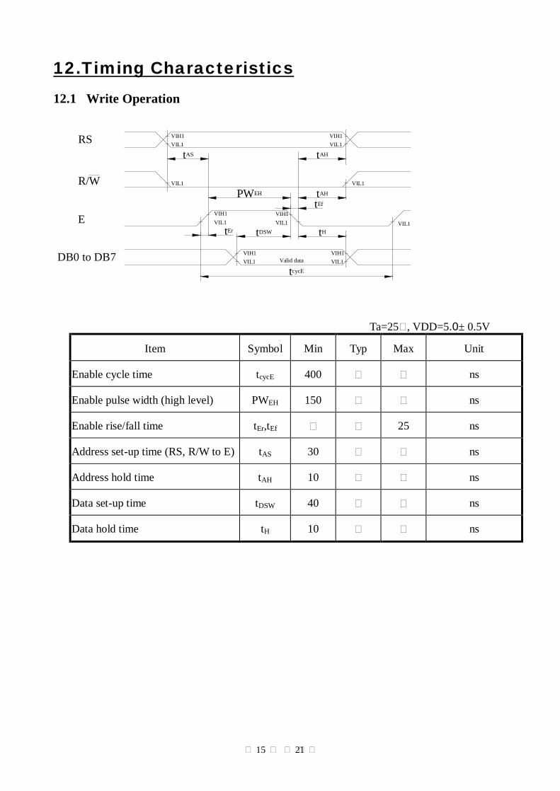
12.Timing Characteristics 12.1 Write Operation
Ta=25 , VDD=5.0± 0.5V Item Symbol Min Typ Max Unit
Enable cycle time tcycE 400 ns
Enable pulse width (high level) PWEH 150 ns
Enable rise/fall time tEr,tEf 25 ns
Address set-up time (RS, R/W to E) tAS 30 ns
Address hold time tAH 10 ns
Data set-up time tDSW 40 ns
Data hold time tH 10 ns
VIH1VIL1
VIH1VIL1
VIL1
tcycE
VIH1VIL1
VIH1VIL1
VIL1
tAS tAH
tAHtEf
tHtDSW
PWEH
tErVIL1
VIH1VIL1
VIH1VIL1
RS
R/W
E
DB0 to DB7 Valid data

16 21
12.2 Read Operation
Ta=25 , VDD=5.0± 0.5V Item Symbol Min Typ Max Unit
Enable cycle time tcycE 400 ns
Enable pulse width (high level) PWEH 150 ns
Enable rise/fall time tEr,tEf 25 ns
Address set-up time (RS, R/W to E) tAS 30 ns
Address hold time tAH 10 ns
Data delay time tDDR 100 ns
Data hold time tDHR 20 ns
VIH1VIL1
VIH1VIL1
tcycE
VOH1VOL1*
tAS tAH
tAHtEf
tDHR
PWEH
tErVIL1
VIH1VIL1
VIH1VIL1
RS
R/W
E
DB0 to DB7
VIH1 VIH1
VOH1*VOL1Valid data
tDDR
NOTE: *VOL1 is assumed to be 0.8V at 2 MHZ operation.

17 21
13.Initializing of LCM
Power on
RS R/W DB7 DB6 DB5 DB4 DB3 DB2 DB1 DB00 0 0 0 1 1 * * * *
Wait for more than 15 ms after VCC rises to 4.5 V
Wait for more than 4.1 ms
1DB4DB7
0RS
0R/W DB6
0 0DB5
1DB1DB2DB3
* * * *DB0
Wait for more than 100 µs
DB41
DB7R/WRS0 0
DB5DB60 0 1
DB1DB3 DB2* * *
DB0*
1DB4DB7
00RS R/W
10 0DB6 DB5 DB1
F *NDB2DB3
*DB0
0 0 0 0 0 0 1 0 0 00 0 0 0 0 0 0 0 0 10 0 0 0 0 0 0 1 I/D S
Initialization ends
BF can not be checked before this instruction.Function set ( Interface is 8 bits long. )
Function set ( Interface is 8 bits long. )
BF can not be checked before this instruction.
BF can not be checked before this instruction.
Function set ( Interface is 8 bits long. )
BF can be checked after the following instructions.When BF is not checked , the waiting time betweeninstructions is longer than execution instruction time.
Function set ( Interface is 8 bits long. Specifythe number of display lines and font. )The number of display lines and character fontcan not be changed after this point.
8-Bit Ineterface
Display offDisplay clearEntry mode set

18 21
Power on
RS R/W DB7 DB6 DB5 DB40 0 0 0 1 1
Wait for more than 15 ms after VCC rises to 4.5 V
Wait for more than 4.1 ms
Wait for more than 100 µs
0DB4DB7
00RS R/W
10 0DB6 DB5
0 0 0 0 1 00 0 N F * *0 0 0 0 0 0
Initialization ends
BF can not be checked before this instruction.Function set ( Interface is 8 bits long. )
Function set ( Interface is 8 bits long. )
BF can not be checked before this instruction.
BF can not be checked before this instruction.
Function set ( Interface is 8 bits long. )
BF can be checked after the following instructions.When BF is not checked , the waiting time betweeninstructions is longer than execution instruction time.
Function set ( Set interface to be 4 bits long. )Interface is 8 bits in length.
Function set ( Interface is 4 bits long. Specifythe number of display lines and character font. )The number of display lines and character fontcan not be changed after this point.Display offDisplay clearEntry mode set
4-Bit Ineterface
0DB6RS R/W
0 0DB7
0DB4DB5
1 1
DB60
RS R/W0 0
DB70
DB4DB51 1
0 0 1 0 0 00 0 0 0 0 00 0 0 0 0 10 0 0 0 0 00 0 0 I/D S1

19 21
14.Quality Assurance Screen Cosmetic Criteria
Item Defect Judgment Criterion Partition
1 Spots
A)Clear Size: d mm Acceptable Qty in active area
d 0.1 Disregard 0.1<d 0.2 6 0.2<d 0.3 2 0.3<d 0
Note: Including pin holes and defective dots which must be within one pixel size.
B)Unclear Size: d mm Acceptable Qty in active area
d 0.2 Disregard 0.2<d 0.5 6 0.5<d 0.7 2 0.7<d 0
Minor
2 Bubbles in Polarize
Size: d mm Acceptable Qty in active area d 0.3 Disregard
0.3<d 1.0 3 1.0<d 1.5 1 1.5<d 0
Minor
3 Scratch In accordance with spots cosmetic criteria. When the light
reflects on the panel surface, the scratches are not to be remarkable.
Minor
4 Allowable Density Above defects should be separated more than 30mm each other. Minor
5 Coloration Not to be noticeable coloration in the viewing area of the
LCD panels. Back-light type should be judged with back-light on state
only. Minor

20 21
15.Reliability Content of Reliability Test
Environmental Test
Test Item Content of Test Test Condition Applicable Standard
High Temperature storage
Endurance test applying the high storage temperature for a long time.
80 200hrs ——
Low Temperature storage
Endurance test applying the high storage temperature for a long time.
-30 200hrs ——
High Temperature Operation
Endurance test applying the electric stress (Voltage & Current) and the thermal stress to the element for a long time.
70 200hrs ——
Low Temperature Operation
Endurance test applying the electric stress under low temperature for a long time.
-20 200hrs ——
High Temperature/ Humidity Storage
Endurance test applying the high temperature and high humidity storage for a long time.
80 ,90%RH 96hrs ——
High Temperature/ Humidity Operation
Endurance test applying the electric stress (Voltage & Current) and temperature / humidity stress to the element for a long time.
70 ,90%RH 96hrs ——
Temperature Cycle
Endurance test applying the low and high temperature cycle. -30 25 80 30min 5min 30min 1 cycle
-30 /80 10 cycles ——
Mechanical Test
Vibration test Endurance test applying the vibration during transportation and using.
10~22Hz→1.5mmp-p 22~500Hz→1.5G Total 0.5hrs
——
Shock test Constructional and mechanical endurance test applying the shock during transportation.
50G Half sign wave 11 msedc 3 times of each direction
——
Atmospheric pressure test
Endurance test applying the atmospheric pressure during transportation by air.
115mbar 40hrs ——
Others
Static electricity test
Endurance test applying the electric stress to the terminal.
VS=800V,RS=1.5kΩ CS=100pF 1 time
——
***Supply voltage for logic system=5V. Supply voltage for LCD system =Operating voltage at 25

21 21
16.Backlight Information Specification
PARAMETER SYMBOL MIN TYP MAX UNIT TEST CONDITION Supply Current ILED ─ 100 mA V=4.2V Supply Voltage V 4.2 4.6 V Reverse Voltage VR 8 V Luminous Intensity IV 60 CD/M2 ILED=100mA
Wave Length λp ─ 570 nm ILED=100mA Life Time 100000 Hr. V 4.6V Color Yellow Green