Embed Size (px)
Citation preview
Samsung V-NAND
Yield more capacity, performance and power efficiency
White Paper

White Paper
Introduction
There continues to be an explosive growth in data traffic
worldwide, pushing NAND flash memory to its limits. Current
2D planar NAND technology has inherent limitations, preventing
capacity expansion that would result in critical degradation
of performance and reliability. Since 2D planar NAND cannot
effectively scale capacity to meet increasing data demand, new
solutions must be found.
Samsung offers an innovative solution to satisfy rising data
demands with its cutting-edge, 3bit vertical-NAND (V-NAND)
flash technology. By stacking memory cells vertically in a three-
dimensional structure, new potential for 3D memory capacities
are created, eliminating performance and reliability issues from
capacity limitations. Whether end consumers or data centers,
everyone can expect smooth, reliable performance at lower
costs for today's demanding, data-centric world.
Traditional 2D planar NAND technology
A typical NAND flash chip is composed of memory cells on a
plane that enables memory write capabilities. The more cells
there are, the greater the memory capacity. Manufacturers strive
to fit more cells in less space and in merely 15 years cell size
has gone from 120 nm to 19 nm with 100 times more capacity,
reaching today's cell size of 1x nm.
Cell-to-cell interference
Continually shrinking the cells creates technical challenges that
arise from an electrical charge in a cell flowing into an adjacent
cell creating cell-to-cell interference. This cell-to-cell interference
unfortunately leads to data corruption. And when a cell size goes
below 20 nm, the chance for interference drastically increases,
inevitably making the cell unreliable.
Prohibitive patterning
Patterning is a photolithography process that uses light to
transfer a geometric pattern from a mask to a photoresist
on the substrate of the chip to create a circuit. With a 1x nm
sized cell, light is unable to penetrate the mask. Effective,
shorter wavelength light equipment is an alternative, but is cost
prohibitive.
Samsung 3bit V-NAND memory technology
Samsung’s revolutionary 3bit V-NAND technology features
a unique design that stacks 32 layers of 3bit cells on top of
one another instead of trying to decrease the cells' length and
width to fit into today's ever-shrinking form factors. Using this
new V-NAND architecture creates two times the density of a
traditional 2D planar NAND in a smaller footprint.
Compared to Samsung's 2-bit 32-layer V-NAND technology, the
3bit V-NAND flash has crossed the threshold of costs in dollars
per gigabit by being able to store 3 bits per cell over 2 bits per
cell. This disruptive density 3bit technology brings costs down,
yet still offers better endurance for consumer and enterprise
applications. By delivering cost, value and density, it enables
Samsung to increase the level of support for next-generation
interfaces, advancing the SSD market.
This innovative design eliminates pattern limitations while
achieving a much larger scalable capacity to satisfy present and
future data demands. V-NAND’s unique design is achieved by
disruptive innovation of structure, material and integration.
Stay abreast of increasing data demands with Samsung's innovative vertical architecture
2
24
Three sixty Residences(24 Floors)
101 California Street(~48 Floors) Effectively
1st V-NAND Mass Product
32 Stack 3bitOne California
(32 Floors)
New Era of V-NAND
Disruptive Density
24 Stack 2bit
32 Stack 2bit32
2nd V-NAND Innovation New Innovation (3bit)
White Paper
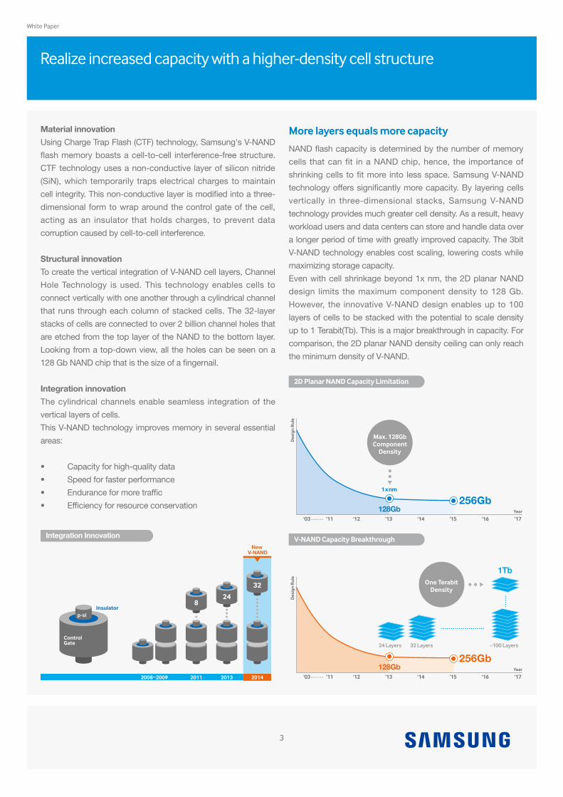
Material innovation
Using Charge Trap Flash (CTF) technology, Samsung's V-NAND
flash memory boasts a cell-to-cell interference-free structure.
CTF technology uses a non-conductive layer of silicon nitride
(SiN), which temporarily traps electrical charges to maintain
cell integrity. This non-conductive layer is modified into a three-
dimensional form to wrap around the control gate of the cell,
acting as an insulator that holds charges, to prevent data
corruption caused by cell-to-cell interference.
Structural innovation
To create the vertical integration of V-NAND cell layers, Channel
Hole Technology is used. This technology enables cells to
connect vertically with one another through a cylindrical channel
that runs through each column of stacked cells. The 32-layer
stacks of cells are connected to over 2 billion channel holes that
are etched from the top layer of the NAND to the bottom layer.
Looking from a top-down view, all the holes can be seen on a
128 Gb NAND chip that is the size of a fingernail.
Integration innovation
The cylindrical channels enable seamless integration of the
vertical layers of cells.
This V-NAND technology improves memory in several essential
areas:
• Capacityforhigh-qualitydata
• Speedforfasterperformance
• Enduranceformoretraffic
• Efficiencyforresourceconservation
More layers equals more capacity
NAND flash capacity is determined by the number of memory
cells that can fit in a NAND chip, hence, the importance of
shrinking cells to fit more into less space. Samsung V-NAND
technology offers significantly more capacity. By layering cells
vertically in three-dimensional stacks, Samsung V-NAND
technology provides much greater cell density. As a result, heavy
workload users and data centers can store and handle data over
a longer period of time with greatly improved capacity. The 3bit
V-NAND technology enables cost scaling, lowering costs while
maximizing storage capacity.
Even with cell shrinkage beyond 1x nm, the 2D planar NAND
design limits the maximum component density to 128 Gb.
However, the innovative V-NAND design enables up to 100
layers of cells to be stacked with the potential to scale density
up to 1 Terabit(Tb). This is a major breakthrough in capacity. For
comparison, the 2D planar NAND density ceiling can only reach
the minimum density of V-NAND.
Realize increased capacity with a higher-density cell structure
3
Integration Innovation
ControlGate
p-siInsulator
248
32
New V-NAND
2008~2009 2011 2013 2014
2D Planar NAND Capacity Limitation
V-NAND Capacity Breakthrough
128Gb
1 x nm
256Gb
Max. 128GbComponent
Density
Des
ign
Rul
e
Year
‘03 . . . . . . ’11 ‘12 ’13 ‘14 ’15 ‘16 ’17
24 Layers 32 Layers ~100 Layers
1Tb
128Gb256Gb
Des
ign
Rul
e
Year
‘03 . . . . . . ’11 ‘12 ’13 ‘14 ’15 ‘16 ’17
One TerabitDensity
White Paper
Double data write speeds compared with 2D NANDwith unique algorithms
4
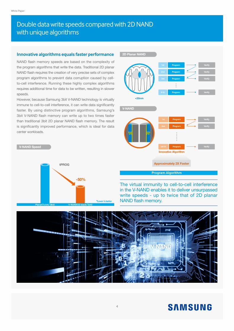
Innovative algorithms equals faster performance
NAND flash memory speeds are based on the complexity of
the program algorithms that write the data. Traditional 2D planar
NAND flash requires the creation of very precise sets of complex
program algorithms to prevent data corruption caused by cell-
to-cell interference. Running these highly complex algorithms
requires additional time for data to be written, resulting in slower
speeds.
However, because Samsung 3bit V-NAND technology is virtually
immune to cell-to-cell interference, it can write data significantly
faster. By using distinctive program algorithms, Samsung’s
3bit V-NAND flash memory can write up to two times faster
than traditional 3bit 2D planar NAND flash memory. The result
is significantly improved performance, which is ideal for data
center workloads.
The virtual immunity to cell-to-cell interference in the V-NAND enables it to deliver unsurpassed write speeds - up to twice that of 2D planar NAND flash memory.
V-NAND Speed
tPROG
*Lower is better
-50%
Planar(1xnm/3bit) V-NAND(32 stack/3bit)
<20nm
1st Program Verify
2nd Program Verify
3rd Program Verify
N th Program Verify
Verify
Verify
Verify
1st
2nd
½N th
Program
Program
Program
2D Planar NAND
V-NAND
Approximately 2X Faster
Innovative Algorithm
Program Algorithm
White Paper
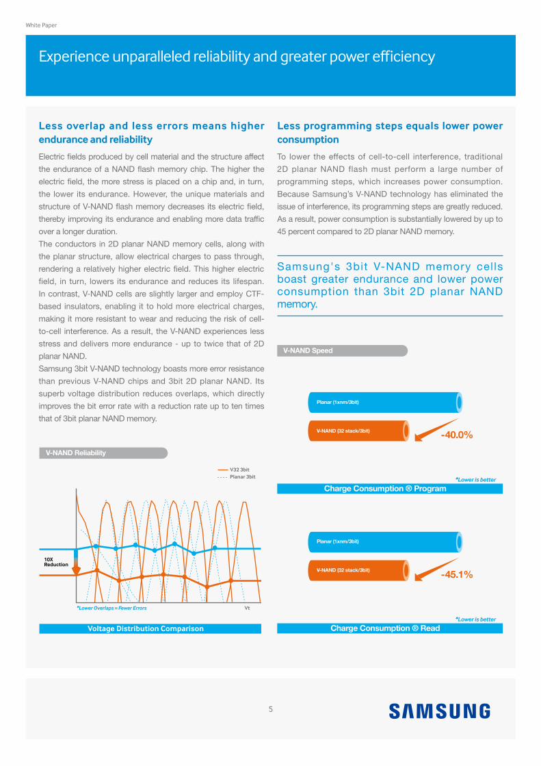
Less overlap and less errors means higher endurance and reliability
Electric fields produced by cell material and the structure affect
the endurance of a NAND flash memory chip. The higher the
electric field, the more stress is placed on a chip and, in turn,
the lower its endurance. However, the unique materials and
structure of V-NAND flash memory decreases its electric field,
thereby improving its endurance and enabling more data traffic
over a longer duration.
The conductors in 2D planar NAND memory cells, along with
the planar structure, allow electrical charges to pass through,
rendering a relatively higher electric field. This higher electric
field, in turn, lowers its endurance and reduces its lifespan.
In contrast, V-NAND cells are slightly larger and employ CTF-
based insulators, enabling it to hold more electrical charges,
making it more resistant to wear and reducing the risk of cell-
to-cell interference. As a result, the V-NAND experiences less
stress and delivers more endurance - up to twice that of 2D
planar NAND.
Samsung 3bit V-NAND technology boasts more error resistance
than previous V-NAND chips and 3bit 2D planar NAND. Its
superb voltage distribution reduces overlaps, which directly
improves the bit error rate with a reduction rate up to ten times
that of 3bit planar NAND memory.
Less programming steps equals lower power consumption
To lower the effects of cell-to-cell interference, traditional
2D planar NAND flash must perform a large number of
programming steps, which increases power consumption.
Because Samsung’s V-NAND technology has eliminated the
issue of interference, its programming steps are greatly reduced.
As a result, power consumption is substantially lowered by up to
45 percent compared to 2D planar NAND memory.
Experience unparalleled reliability and greater power efficiency
5
Samsung's 3bit V-NAND memory cel ls boast greater endurance and lower power consumption than 3bit 2D planar NAND memory.
V-NAND Reliability
10XReduction
*Lower Overlaps = Fewer Errors Vt
V32 3bitPlanar 3bit
Voltage Distribution Comparison
V-NAND Speed
-40.0%
Planar(1xnm/3bit)
*Lower is better
-45.1%
*Lower is better
Planar (1xnm/3bit)
V-NAND (32 stack/3bit)
Planar (1xnm/3bit)
V-NAND (32 stack/3bit)
Charge Consumption ® Program
Charge Consumption ® Read

White Paper
Improve capacity, performance, endurance and power efficiency
Legal and additional information
6
Conclusion
Samsung 3bit V-NAND flash technology overcomes the
capacity limitations of traditional 2D planar NAND technology
with its revolutionary vertical, three-dimensional design. This
innovative 3D vertical architecture insulates individual cells
from interference and increases density to eliminate patterning
restrictions.
In addition, the innovations that V-NAND flash provide enable
higher cell density for greater capacity, simplified programming
for enhanced speed and power efficiency, and robust materials
for greater endurance over the lifespan of the flash memory.
Samsung V-NAND flash memory is the smart choice for fulfilling
the ever-increasing demands of today's - and tomorrow's - data
centers.
Choose flash memory designed by a pioneer in V-NAND technology
Samsung has gained a wealth of knowledge and expertise as
a global leader in memory innovations, which spans more than
two decades. Over those years, Samsung boasts a number of
market firsts, including the first SSD, the first 2-bit MLC SSD,
the first 3bit SSD and the first PCle PC SSD.
In particular, Samsung is a major innovator in V-NAND memory
technology and the first company to mass-produce V-NAND-
equipped SSDs. And now Samsung is the first to develop the
32-stack 3bit
V-NAND. No wonder so many data centers are entrusting
Samsung flash memory to manage their valuable data.
About Samsung Electronics Co., Ltd.
Samsung Electronics Co., Ltd. is a global leader in technology,
opening new possibilities for people everywhere. Through
relentless innovation and discovery, we are transforming
the worlds of TVs, smartphones, tablets, PCs, cameras,
home appliances, printers, LTE systems, medical devices,
semiconductors and LED solutions. We employ 286,000 people
across 80 countries with annual sales of US$216.7 billion.
To discover more, please visit www.samsung.com.
For more information
For more information about Samsung 3bit V-NAND flash
memory, visit
www.samsung.com/semiconductor
Copyright © 2015 Samsung Electronics Co., Ltd. All rights
reserved. Samsung is a registered trademark of Samsung
Electronics Co., Ltd. Specifications and designs are subject to
change without notice. Nonmetric weights and measurements
are approximate. All data were deemed correct at time of
creation. Samsung is not liable for errors or omissions. All
brand, product, service names and logos are trademarks and/or
registered trademarks of their respective owners and are hereby
recognized and acknowledged.
Samsung Electronics Co., Ltd.
416, Maetan 3-dong, Yeongtong-gu, Suwon-si, Gyeonggi-do
443-772, Korea
www.samsung.com
2015-08
Samsung has been a global leader in designing and manufacturing cutting-edge memory technology spanning more than two decades.