Embed Size (px)
Citation preview
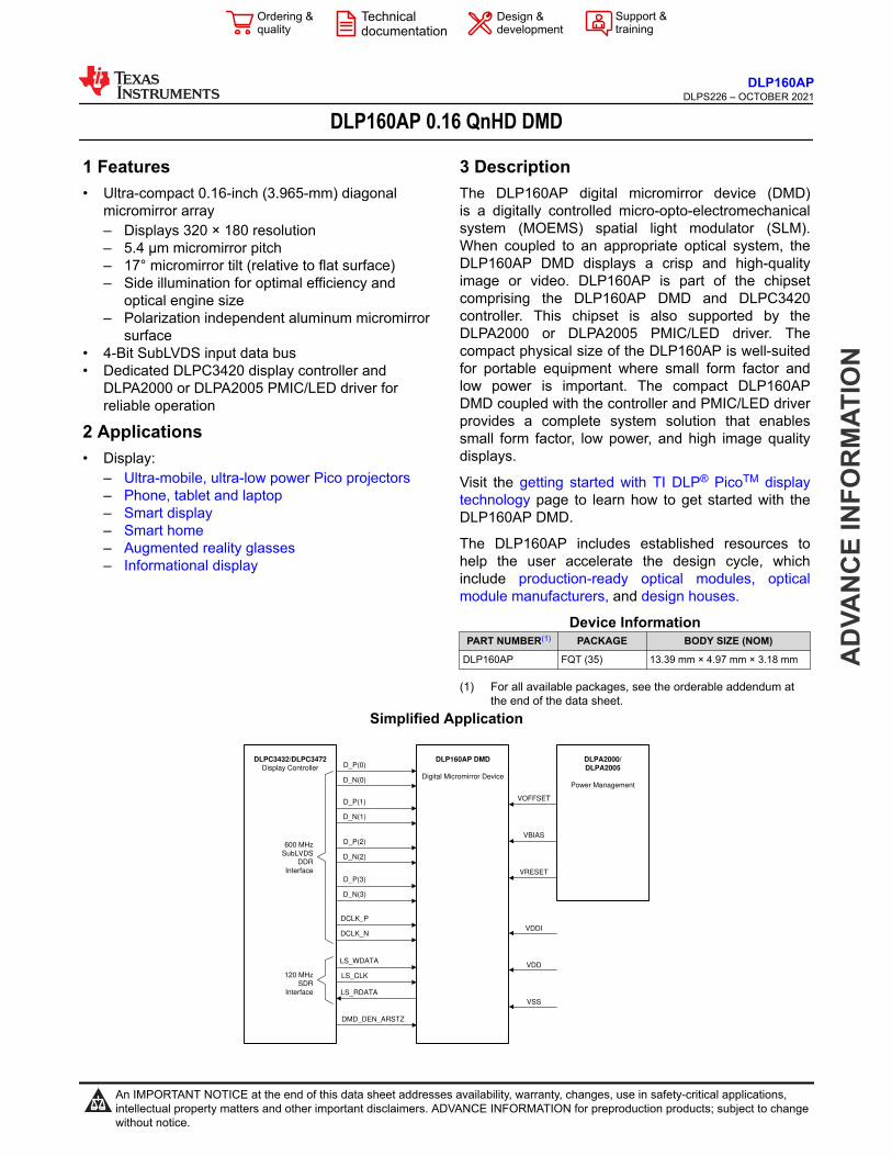
DLP160AP 0.16 QnHD DMD
1 Features• Ultra-compact 0.16-inch (3.965-mm) diagonal
micromirror array– Displays 320 × 180 resolution– 5.4 µm micromirror pitch– 17° micromirror tilt (relative to flat surface)– Side illumination for optimal efficiency and
optical engine size– Polarization independent aluminum micromirror
surface• 4-Bit SubLVDS input data bus• Dedicated DLPC3420 display controller and
DLPA2000 or DLPA2005 PMIC/LED driver for reliable operation
2 Applications• Display:
– Ultra-mobile, ultra-low power Pico projectors– Phone, tablet and laptop– Smart display– Smart home– Augmented reality glasses– Informational display
3 DescriptionThe DLP160AP digital micromirror device (DMD) is a digitally controlled micro-opto-electromechanical system (MOEMS) spatial light modulator (SLM). When coupled to an appropriate optical system, the DLP160AP DMD displays a crisp and high-quality image or video. DLP160AP is part of the chipset comprising the DLP160AP DMD and DLPC3420 controller. This chipset is also supported by the DLPA2000 or DLPA2005 PMIC/LED driver. The compact physical size of the DLP160AP is well-suited for portable equipment where small form factor and low power is important. The compact DLP160AP DMD coupled with the controller and PMIC/LED driver provides a complete system solution that enables small form factor, low power, and high image quality displays.
Visit the getting started with TI DLP® PicoTM display technology page to learn how to get started with the DLP160AP DMD.
The DLP160AP includes established resources to help the user accelerate the design cycle, which include production-ready optical modules, optical module manufacturers, and design houses.
Device InformationPART NUMBER(1) PACKAGE BODY SIZE (NOM)
DLP160AP FQT (35) 13.39 mm × 4.97 mm × 3.18 mm
(1) For all available packages, see the orderable addendum at the end of the data sheet.
Simplified Application
D_P(0)
D_N(0)
D_P(1)
D_N(1)
DLPC3432/DLPC3472
Display Controller
D_P(2)
D_N(2)
D_P(3)
D_N(3)
DCLK_P
DCLK_N
LS_WDATA
LS_CLK
LS_RDATA
600 MHz
SubLVDS
DDR
Interface
DMD_DEN_ARSTZ
DLP160AP DMD
Digital Micromirror Device
VOFFSET
VBIAS
VRESET
VDDI
VDD
VSS
DLPA2000/
DLPA2005
Power Management
120 MHz
SDR
Interface
AD
VAN
CE
INFO
RM
ATIO
N
DLP160APDLPS226 – OCTOBER 2021
An IMPORTANT NOTICE at the end of this data sheet addresses availability, warranty, changes, use in safety-critical applications, intellectual property matters and other important disclaimers. ADVANCE INFORMATION for preproduction products; subject to change without notice.
Table of Contents1 Features............................................................................12 Applications..................................................................... 13 Description.......................................................................14 Revision History.............................................................. 25 Pin Configuration and Functions...................................36 Specifications.................................................................. 6
6.1 Absolute Maximum Ratings........................................ 66.2 Storage Conditions..................................................... 66.3 ESD Ratings............................................................... 76.4 Recommended Operating Conditions.........................76.5 Thermal Information..................................................106.6 Electrical Characteristics...........................................106.7 Timing Requirements................................................ 116.8 Switching Characteristics(1) ..................................... 166.9 System Mounting Interface Loads............................ 176.10 Micromirror Array Physical Characteristics............. 186.11 Micromirror Array Optical Characteristics............... 196.12 Window Characteristics.......................................... 206.13 Chipset Component Usage Specification............... 20
7 Detailed Description......................................................217.1 Overview................................................................... 217.2 Functional Block Diagram......................................... 217.3 Feature Description...................................................227.4 Device Functional Modes..........................................22
7.5 Optical Interface and System Image Quality Considerations............................................................ 22
7.6 Micromirror Array Temperature Calculation.............. 237.7 Micromirror Landed-On/Landed-Off Duty Cycle....... 24
8 Application and Implementation.................................. 288.1 Application Information............................................. 288.2 Typical Application.................................................... 29
9 Power Supply Recommendations................................319.1 Power Supply Power-Up Procedure......................... 319.2 Power Supply Power-Down Procedure.....................319.3 Power Supply Sequencing Requirements................ 32
10 Layout...........................................................................3410.1 Layout Guidelines................................................... 3410.2 Layout Example...................................................... 34
11 Device and Documentation Support..........................3511.1 Device Support........................................................3511.2 Receiving Notification of Documentation Updates.. 3511.3 Support Resources................................................. 3511.4 Trademarks............................................................. 3511.5 Electrostatic Discharge Caution.............................. 3511.6 Glossary.................................................................. 36
12 Mechanical, Packaging, and Orderable Information.................................................................... 36
4 Revision HistoryDATE REVISION NOTES
October 2021 * Initial release.
DLP160APDLPS226 – OCTOBER 2021 www.ti.com
AD
VAN
CE IN
FOR
MATIO
N
2 Submit Document Feedback Copyright © 2021 Texas Instruments Incorporated
Product Folder Links: DLP160AP
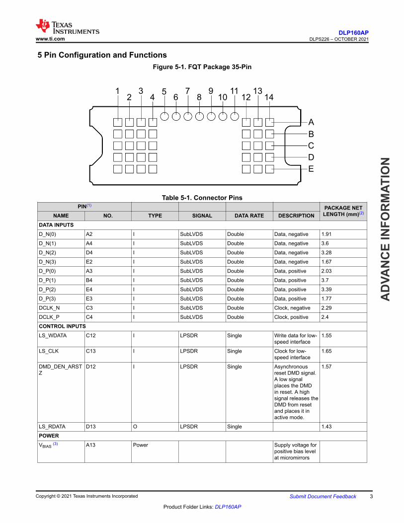
5 Pin Configuration and FunctionsFigure 5-1. FQT Package 35-Pin
14856
1110
912
7 131234
A
B
C
D
E
Table 5-1. Connector PinsPIN(1) PACKAGE NET
LENGTH (mm)(2)NAME NO. TYPE SIGNAL DATA RATE DESCRIPTIONDATA INPUTSD_N(0) A2 I SubLVDS Double Data, negative 1.91
D_N(1) A4 I SubLVDS Double Data, negative 3.6
D_N(2) D4 I SubLVDS Double Data, negative 3.28
D_N(3) E2 I SubLVDS Double Data, negative 1.67
D_P(0) A3 I SubLVDS Double Data, positive 2.03
D_P(1) B4 I SubLVDS Double Data, positive 3.7
D_P(2) E4 I SubLVDS Double Data, positive 3.39
D_P(3) E3 I SubLVDS Double Data, positive 1.77
DCLK_N C3 I SubLVDS Double Clock, negative 2.29
DCLK_P C4 I SubLVDS Double Clock, positive 2.4
CONTROL INPUTSLS_WDATA C12 I LPSDR Single Write data for low-
speed interface1.55
LS_CLK C13 I LPSDR Single Clock for low-speed interface
1.65
DMD_DEN_ARSTZ
D12 I LPSDR Single Asynchronous reset DMD signal. A low signal places the DMD in reset. A high signal releases the DMD from reset and places it in active mode.
1.57
LS_RDATA D13 O LPSDR Single 1.43
POWERVBIAS (3) A13 Power Supply voltage for
positive bias level at micromirrors
www.ti.comDLP160AP
DLPS226 – OCTOBER 2021
AD
VAN
CE
INFO
RM
ATIO
N
Copyright © 2021 Texas Instruments Incorporated Submit Document Feedback 3
Product Folder Links: DLP160AP
Table 5-1. Connector Pins (continued)PIN(1) PACKAGE NET
LENGTH (mm)(2)NAME NO. TYPE SIGNAL DATA RATE DESCRIPTIONVOFFSET (3) E13 Power Supply voltage
for HVCMOS core logic. Supply voltage for stepped high level at micromirror address electrodes. Supply voltage for offset level at micromirrors.
VRESET (3) A14 Power Supply voltage for negative reset level at micromirrors.
VDD B12 Power Supply voltage for LVCMOS core logic. Supply voltage for LPSDR inputs. Supply voltage for normal high level at micromirror address electrodes.
VDD B14 Power
VDD C1 Power
VDD C14 Power
VDD C2 Power
VDD E14 Power
VDDI B1 Power Supply voltage for SubLVDS receivers.VDDI D1 Power
VSS A1 Ground Common return. Ground for all power.VSS A12 Ground
VSS B13 Ground
VSS B2 Ground
VSS B3 Ground
VSS D14 Ground
VSS D2 Ground
VSS D3 Ground
VSS E1 Ground
VSS E12 Ground
(1) Low speed interface is LPSDR and adheres to the Electrical Characteristics and AC/DC Operating Conditions table in JEDEC Standard No. 209B, Low Power Double Data Rate (LPDDR). See JESD209B.
(2) Net trace lengths inside the package:Relative dielectric constant for the FQP ceramic package is 9.8.Propagation speed = 11.8 / sqrt (9.8) = 3.769 in/ns.Propagation delay = 0.265 ns/inch = 265 ps/in = 10.43 ps/mm.
(3) The following power supplies are all required to operate the DMD: VDD, VDDI, VOFFSET, VBIAS, VRESET. All VSS connections are also required.
Table 5-2. Test PadsNUMBER SYSTEM BOARD
A5 Do not connect
A6 Do not connect
A7 Do not connect
A8 Do not connect
A9 Do not connect
DLP160APDLPS226 – OCTOBER 2021 www.ti.com
AD
VAN
CE IN
FOR
MATIO
N
4 Submit Document Feedback Copyright © 2021 Texas Instruments Incorporated
Product Folder Links: DLP160AP
Table 5-2. Test Pads (continued)NUMBER SYSTEM BOARD
A10 Do not connect
A11 Do not connect
www.ti.comDLP160AP
DLPS226 – OCTOBER 2021
AD
VAN
CE
INFO
RM
ATIO
N
Copyright © 2021 Texas Instruments Incorporated Submit Document Feedback 5
Product Folder Links: DLP160AP
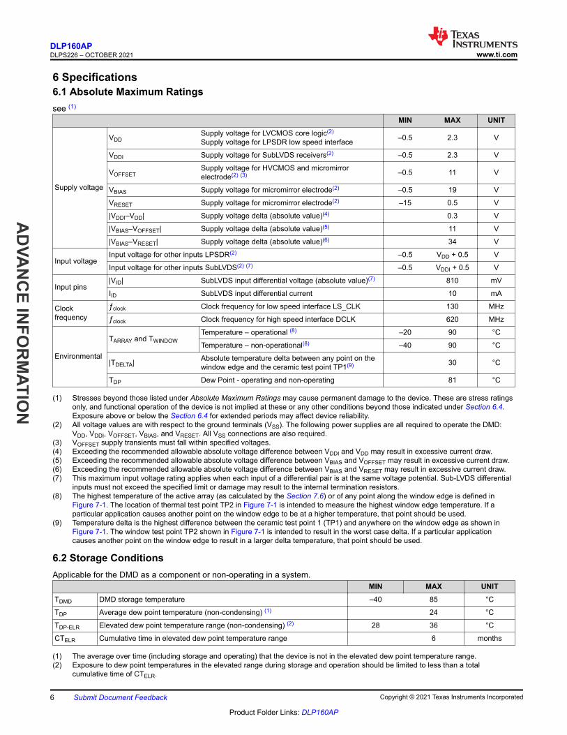
6 Specifications6.1 Absolute Maximum Ratingssee (1)
MIN MAX UNIT
Supply voltage
VDDSupply voltage for LVCMOS core logic(2)
Supply voltage for LPSDR low speed interface –0.5 2.3 V
VDDI Supply voltage for SubLVDS receivers(2) –0.5 2.3 V
VOFFSETSupply voltage for HVCMOS and micromirror electrode(2) (3) –0.5 11 V
VBIAS Supply voltage for micromirror electrode(2) –0.5 19 V
VRESET Supply voltage for micromirror electrode(2) –15 0.5 V
|VDDI–VDD| Supply voltage delta (absolute value)(4) 0.3 V
|VBIAS–VOFFSET| Supply voltage delta (absolute value)(5) 11 V
|VBIAS–VRESET| Supply voltage delta (absolute value)(6) 34 V
Input voltageInput voltage for other inputs LPSDR(2) –0.5 VDD + 0.5 V
Input voltage for other inputs SubLVDS(2) (7) –0.5 VDDI + 0.5 V
Input pins|VID| SubLVDS input differential voltage (absolute value)(7) 810 mV
IID SubLVDS input differential current 10 mA
Clock frequency
ƒclock Clock frequency for low speed interface LS_CLK 130 MHz
ƒclock Clock frequency for high speed interface DCLK 620 MHz
Environmental
TARRAY and TWINDOWTemperature – operational (8) –20 90 °C
Temperature – non-operational(8) –40 90 °C
|TDELTA| Absolute temperature delta between any point on the window edge and the ceramic test point TP1(9) 30 °C
TDP Dew Point - operating and non-operating 81 °C
(1) Stresses beyond those listed under Absolute Maximum Ratings may cause permanent damage to the device. These are stress ratings only, and functional operation of the device is not implied at these or any other conditions beyond those indicated under Section 6.4. Exposure above or below the Section 6.4 for extended periods may affect device reliability.
(2) All voltage values are with respect to the ground terminals (VSS). The following power supplies are all required to operate the DMD: VDD, VDDI, VOFFSET, VBIAS, and VRESET. All VSS connections are also required.
(3) VOFFSET supply transients must fall within specified voltages.(4) Exceeding the recommended allowable absolute voltage difference between VDDI and VDD may result in excessive current draw.(5) Exceeding the recommended allowable absolute voltage difference between VBIAS and VOFFSET may result in excessive current draw.(6) Exceeding the recommended allowable absolute voltage difference between VBIAS and VRESET may result in excessive current draw.(7) This maximum input voltage rating applies when each input of a differential pair is at the same voltage potential. Sub-LVDS differential
inputs must not exceed the specified limit or damage may result to the internal termination resistors.(8) The highest temperature of the active array (as calculated by the Section 7.6) or of any point along the window edge is defined in
Figure 7-1. The location of thermal test point TP2 in Figure 7-1 is intended to measure the highest window edge temperature. If a particular application causes another point on the window edge to be at a higher temperature, that point should be used.
(9) Temperature delta is the highest difference between the ceramic test point 1 (TP1) and anywhere on the window edge as shown in Figure 7-1. The window test point TP2 shown in Figure 7-1 is intended to result in the worst case delta. If a particular application causes another point on the window edge to result in a larger delta temperature, that point should be used.
6.2 Storage ConditionsApplicable for the DMD as a component or non-operating in a system.
MIN MAX UNITTDMD DMD storage temperature –40 85 °C
TDP Average dew point temperature (non-condensing) (1) 24 °C
TDP-ELR Elevated dew point temperature range (non-condensing) (2) 28 36 °C
CTELR Cumulative time in elevated dew point temperature range 6 months
(1) The average over time (including storage and operating) that the device is not in the elevated dew point temperature range.(2) Exposure to dew point temperatures in the elevated range during storage and operation should be limited to less than a total
cumulative time of CTELR.
DLP160APDLPS226 – OCTOBER 2021 www.ti.com
AD
VAN
CE IN
FOR
MATIO
N
6 Submit Document Feedback Copyright © 2021 Texas Instruments Incorporated
Product Folder Links: DLP160AP
6.3 ESD RatingsVALUE UNIT
V(ESD) Electrostatic discharge Human body model (HBM), per ANSI/ESDA/JEDEC JS-001(1) ±2000 V
(1) JEDEC document JEP155 states that 500-V HBM allows safe manufacturing with a standard ESD control process.
6.4 Recommended Operating ConditionsOver operating free-air temperature range (unless otherwise noted)(1) (2)
MIN NOM MAX UNITSUPPLY VOLTAGE RANGE(3)
VDD Supply voltage for LVCMOS core logicSupply voltage for LPSDR low-speed interface
1.65 1.8 1.95 V
VDDI Supply voltage for SubLVDS receivers 1.65 1.8 1.95 V
VOFFSET Supply voltage for HVCMOS and micromirror electrode(4) 9.5 10 10.5 V
VBIAS Supply voltage for micromirror electrode 17.5 18 18.5 V
VRESET Supply voltage for micromirror electrode –14.5 –14 –13.5 V
|VDDI–VDD| Supply voltage delta (absolute value)(5) 0.3 V
|VBIAS–VOFFSET| Supply voltage delta (absolute value)(6) 10.5 V
|VBIAS–VRESET| Supply voltage delta (absolute value)(7) 33 V
CLOCK FREQUENCYƒclock Clock frequency for low speed interface LS_CLK(8) 108 120 MHz
ƒclock Clock frequency for high speed interface DCLK(9) 300 540 MHz
Duty cycle distortion DCLK 44% 56%
SUBLVDS INTERFACE(9)
|VID| SubLVDS input differential voltage (absolute value). See Figure 6-8, Figure 6-9
150 250 350 mV
VCM Common mode voltage. See Figure 6-8, Figure 6-9 700 900 1100 mV
VSUBLVDS SubLVDS voltage. See Figure 6-8, Figure 6-9 575 1225 mV
ZLINE Line differential impedance (PWB/trace) 90 100 110 Ω
ZIN Internal differential termination resistance. See Figure 6-10
80 100 120 Ω
100-Ω differential PCB trace 6.35 152.4 mm
www.ti.comDLP160AP
DLPS226 – OCTOBER 2021
AD
VAN
CE
INFO
RM
ATIO
N
Copyright © 2021 Texas Instruments Incorporated Submit Document Feedback 7
Product Folder Links: DLP160AP
6.4 Recommended Operating Conditions (continued)Over operating free-air temperature range (unless otherwise noted)(1) (2)
MIN NOM MAX UNITENVIRONMENTALTARRAY Array Temperature – long-term operational(10) (11) (12) (13) 0 40 to 70(12) °C
Array Temperature – short-term operational, 25 hr max(11) (14)
-20 –10 °C
Array Temperature – short-term operational, 500 hr max(11) (14)
-10 0 °C
Array Temperature – short-term operational, 500 hr max(11) (14)
70 75 °C
TWINDOW Window Temperature – operational(15) (16) 90 °C
|TDELTA| Absolute temperature delta between any point on the window edge and the ceramic test point TP1(17)
15 °C
TDP-AVG Average dew point temperature (non-condensing) (18) 24 °C
TDP-ELR Elevated dew point temperature range (non-condensing) (19)
28 36 °C
CTELR Cumulative time in elevated dew point temperature range 6 months
ILLUV Illumination wavelengths < 420 nm (10) 0.68 mW/cm2
ILLVIS Illumination wavelengths between 420 nm and 700 nm Thermally Limited
ILLIR Illumination wavelengths > 700 nm 10 mW/cm2
ILLθ Illumination marginal ray angle(15) 55 degrees
(1) The functional performance of the device specified in this data sheet is achieved when operating the device within the limits defined by the Section 6.4. No level of performance is implied when operating the device above or below the Section 6.4 limits.
(2) The following power supplies are all required to operate the DMD: VDD, VDDI, VOFFSET, VBIAS, and VRESET. All VSS connections are also required.
(3) All voltage values are with respect to the ground pins (VSS).(4) VOFFSET supply transients must fall within specified max voltages.(5) To prevent excess current, the supply voltage delta |VDDI – VDD| must be less than the specified limit.(6) To prevent excess current, the supply voltage delta |VBIAS – VOFFSET| must be less than the specified limit.(7) To prevent excess current, the supply voltage delta |VBIAS – VRESET| must be less than the specified limit.(8) LS_CLK must run as specified to ensure internal DMD timing for reset waveform commands.(9) Refer to the SubLVDS timing requirements in Section 6.7.(10) Simultaneous exposure of the DMD to the maximum Recommended Operating Conditions for temperature and UV illumination will
reduce device lifetime.(11) The array temperature cannot be measured directly and must be computed analytically from the temperature measured at test point 1
(TP1) shown in Figure 7-1 and the package thermal resistance using Section 7.6.(12) Per Figure 6-1, the maximum operational array temperature should be derated based on the micromirror landed duty cycle that the
DMD experiences in the end application. Refer to Section 7.7 for a definition of micromirror landed duty cycle.(13) Long-term is defined as the usable life of the device.(14) Short-term is the total cumulative time over the useful life of the device.(15) The maximum marginal ray angle of the incoming illumination light at any point in the micromirror array, including at the pond of
micromirrors (POM), should not exceed 55 degrees from the normal to the device array plane. The device window aperture has not necessarily been designed to allow incoming light at higher maximum angles to pass to the micromirrors, and the device performance has not been tested nor qualified at angles exceeding this. Illumination light exceeding this angle outside the micromirror array (including POM) will contribute to thermal limitations described in this document and may negatively affect lifetime.
(16) Window temperature is the highest temperature on the window edge shown in Figure 7-1. The location of thermal test point TP2 in Figure 7-1 is intended to measure the highest window edge temperature. If a particular application causes another point on the window edge to be at a higher temperature, that point should be used.
(17) Temperature delta is the highest difference between the ceramic test point 1 (TP1) and anywhere on the window edge shown in Figure 7-1. The window test point TP2 shown in Figure 7-1 is intended to result in the worst-case delta temperature. If a particular application causes another point on the window edge to result in a larger delta temperature, that point should be used.
(18) The average over time (including storage and operating) that the device is not in the 'elevated dew point temperature range'.(19) Exposure to dew point temperatures in the elevated range during storage and operation should be limited to less than a total
cumulative time of CTELR.
DLP160APDLPS226 – OCTOBER 2021 www.ti.com
AD
VAN
CE IN
FOR
MATIO
N
8 Submit Document Feedback Copyright © 2021 Texas Instruments Incorporated
Product Folder Links: DLP160AP
Micromirror Landed Duty Cycle
Opera
tional (°
C)
0/100 5/95 10/90 15/85 20/80 25/75 30/70 35/65 40/60 45/5530
40
50
60
70
80
D001
50/50100/0 95/5 90/10 85/15 80/20 75/25 70/30 65/35 60/40 55/45
Max R
ecom
mended
Arr
ay
Tem
pera
ture
–
Figure 6-1. Maximum Recommended Array Temperature – Derating Curve
www.ti.comDLP160AP
DLPS226 – OCTOBER 2021
AD
VAN
CE
INFO
RM
ATIO
N
Copyright © 2021 Texas Instruments Incorporated Submit Document Feedback 9
Product Folder Links: DLP160AP
6.5 Thermal Information
THERMAL METRIC(1)
DLP160APUNITFQT
35 PINSThermal resistance Active area to test point 1 (TP1)(1) 13 °C/W
(1) The DMD is designed to conduct absorbed and dissipated heat to the back of the package. The cooling system must be capable of maintaining the package within the temperature range specified in the Section 6.4. The total heat load on the DMD is largely driven by the incident light absorbed by the active area, although other contributions include light energy absorbed by the window aperture and electrical power dissipated by the array. Optical systems should be designed to minimize the light energy falling outside the window clear aperture since any additional thermal load in this area can significantly degrade the reliability of the device.
6.6 Electrical CharacteristicsOver operating free-air temperature range (unless otherwise noted)(1)
PARAMETER TEST CONDITIONS(2) MIN TYP MAX UNITCURRENT
IDD Supply current: VDD (3) (4)VDD = 1.95 V 90
mAVDD = 1.8 V 78
IDDI Supply current: VDDI (3) (4)VDDI = 1.95 V 20
mAVDDI = 1.8 V 17
IOFFSET Supply current: VOFFSET (5) (6)VOFFSET = 10.5 V 5
mAVOFFSET = 10 V 4.7
IBIAS Supply current: VBIAS (5) (6)VBIAS = 18.5 V 1.5
mAVBIAS = 18 V 1.4
IRESET Supply current: VRESET (6)VRESET = –14.5 V -2
mAVRESET = –14 V -1.8
POWER(7)
PDD Supply power dissipation: VDD (3) (4)VDD = 1.95 V 175
mWVDD = 1.8 V 141
PDDI Supply power dissipation: VDDI (3) (4)VDDI = 1.95 V 39
mWVDD = 1.8 V 31
POFFSETSupply power dissipation: VOFFSET (5) (6)
VOFFSET = 10.5 V 50mW
VOFFSET = 10 V 44
PBIAS Supply power dissipation: VBIAS (5) (6)VBIAS = 18.5 V 27
mWVBIAS = 18 V 25
PRESET Supply power dissipation: VRESET (6)VRESET = –14.5 V 28
mWVRESET = –14 V 25
PTOTAL Supply power dissipation: Total 263 319 mW
LPSDR INPUT(8)
VIH(DC) DC input high voltage(9) 0.7 × VDD VDD + 0.3 V
VIL(DC) DC input low voltage(9) –0.3 0.3 × VDD V
VIH(AC) AC input high voltage(9) 0.8 × VDD VDD + 0.3 V
VIL(AC) AC input low voltage(9) –0.3 0.2 × VDD V
∆VT Hysteresis ( VT+ – VT– ) Figure 6-10 0.1 × VDD 0.4 × VDD V
IIL Low–level input current VDD = 1.95 V; VI = 0 V –100 nA
IIH High–level input current VDD = 1.95 V; VI = 1.95 V 100 nA
LPSDR OUTPUT(10)
VOH DC output high voltage IOH = –2 mA 0.8 × VDD V
VOL DC output low voltage IOL = 2 mA 0.2 × VDD V
DLP160APDLPS226 – OCTOBER 2021 www.ti.com
AD
VAN
CE IN
FOR
MATIO
N
10 Submit Document Feedback Copyright © 2021 Texas Instruments Incorporated
Product Folder Links: DLP160AP
6.6 Electrical Characteristics (continued)Over operating free-air temperature range (unless otherwise noted)(1)
PARAMETER TEST CONDITIONS(2) MIN TYP MAX UNITCAPACITANCE
CINInput capacitance LPSDR ƒ = 1 MHz 10 pF
Input capacitance SubLVDS ƒ = 1 MHz 10 pF
COUT Output capacitance ƒ = 1 MHz 10 pF
CRESET Reset group capacitance ƒ = 1 MHz; (640 ×360 micromirrors) 90 140 pF
(1) Device electrical characteristics are over Section 6.4 unless otherwise noted.(2) All voltage values are with respect to the ground pins (VSS).(3) To prevent excess current, the supply voltage delta |VDDI – VDD| must be less than the specified limit.(4) Supply power dissipation based on non–compressed commands and data.(5) To prevent excess current, the supply voltage delta |VBIAS – VOFFSET| must be less than the specified limit.(6) Supply power dissipation based on 3 global resets in 200 µs.(7) The following power supplies are all required to operate the DMD: VDD, VDDI, VOFFSET, VBIAS, VRESET. All VSS connections are also
required.(8) LPSDR specifications are for pins LS_CLK and LS_WDATA.(9) Low-speed interface is LPSDR and adheres to the Electrical Characteristics and AC/DC Operating Conditions table in JEDEC
Standard No. 209B, Low-Power Double Data Rate (LPDDR) JESD209B.(10) LPSDR specification is for pin LS_RDATA.
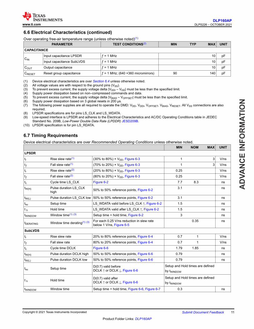
6.7 Timing RequirementsDevice electrical characteristics are over Recommended Operating Conditions unless otherwise noted.
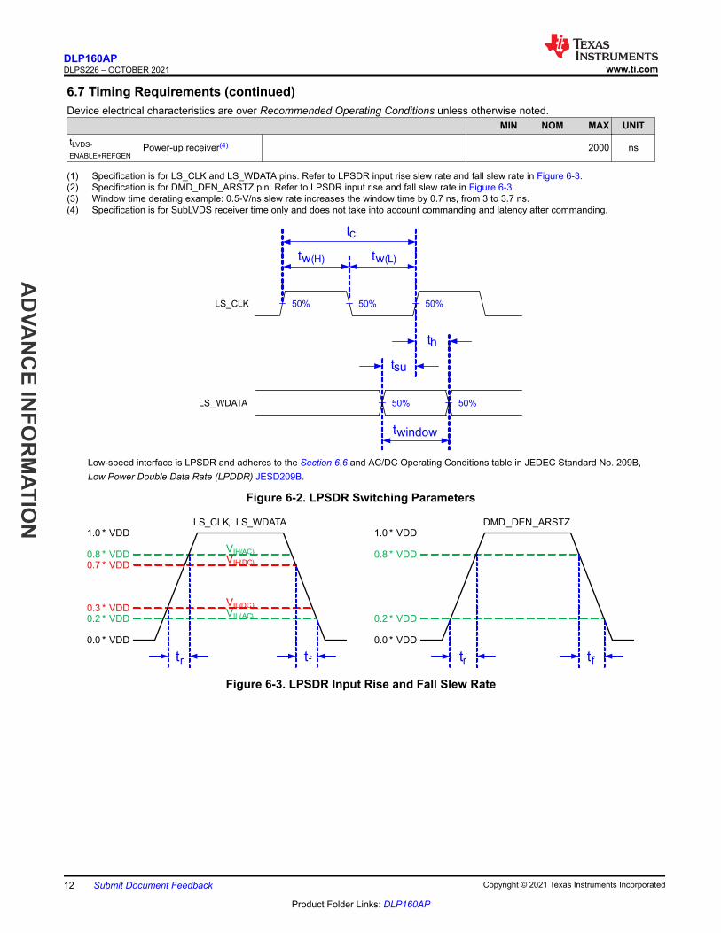
MIN NOM MAX UNITLPSDRtr Rise slew rate(1) (30% to 80%) × VDD, Figure 6-3 1 3 V/ns
tƒ Fall slew rate(1) (70% to 20%) × VDD, Figure 6-3 1 3 V/ns
tr Rise slew rate(2) (20% to 80%) × VDD, Figure 6-3 0.25 V/ns
tƒ Fall slew rate(2) (80% to 20%) × VDD, Figure 6-3 0.25 V/ns
tc Cycle time LS_CLK Figure 6-2 7.7 8.3 ns
tW(H) Pulse duration LS_CLK high 50% to 50% reference points, Figure 6-2 3.1 ns
tW(L) Pulse duration LS_CLK low 50% to 50% reference points, Figure 6-2 3.1 ns
tsu Setup time LS_WDATA valid before LS_CLK ↑, Figure 6-2 1.5 ns
t h Hold time LS_WDATA valid after LS_CLK ↑, Figure 6-2 1.5 ns
tWINDOW Window time(1) (3) Setup time + hold time, Figure 6-2 3 ns
tDERATING Window time derating(1) (3) For each 0.25 V/ns reduction in slew rate below 1 V/ns, Figure 6-5
0.35 ns
SubLVDStr Rise slew rate 20% to 80% reference points, Figure 6-4 0.7 1 V/ns
tƒ Fall slew rate 80% to 20% reference points, Figure 6-4 0.7 1 V/ns
tc Cycle time DCLK Figure 6-6 1.79 1.85 ns
tW(H) Pulse duration DCLK high 50% to 50% reference points, Figure 6-6 0.79 ns
tW(L) Pulse duration DCLK low 50% to 50% reference points, Figure 6-6 0.79 ns
tsu Setup time D(0:7) valid beforeDCLK ↑ or DCLK ↓, Figure 6-6
Setup and Hold times are defined by tWINDOW
t h Hold time D(0:7) valid afterDCLK ↑ or DCLK ↓, Figure 6-6
Setup and Hold times are defined by tWINDOW
tWINDOW Window time Setup time + hold time, Figure 6-6, Figure 6-7 0.3 ns
www.ti.comDLP160AP
DLPS226 – OCTOBER 2021
AD
VAN
CE
INFO
RM
ATIO
N
Copyright © 2021 Texas Instruments Incorporated Submit Document Feedback 11
Product Folder Links: DLP160AP
6.7 Timing Requirements (continued)Device electrical characteristics are over Recommended Operating Conditions unless otherwise noted.
MIN NOM MAX UNITtLVDS-ENABLE+REFGEN
Power-up receiver(4) 2000 ns
(1) Specification is for LS_CLK and LS_WDATA pins. Refer to LPSDR input rise slew rate and fall slew rate in Figure 6-3.(2) Specification is for DMD_DEN_ARSTZ pin. Refer to LPSDR input rise and fall slew rate in Figure 6-3.(3) Window time derating example: 0.5-V/ns slew rate increases the window time by 0.7 ns, from 3 to 3.7 ns.(4) Specification is for SubLVDS receiver time only and does not take into account commanding and latency after commanding.
LS_WDATA
LS_CLK
tw(H) tw(L)
tc
50%50%50%
50% 50%
th
tsu
twindow
Low-speed interface is LPSDR and adheres to the Section 6.6 and AC/DC Operating Conditions table in JEDEC Standard No. 209B, Low Power Double Data Rate (LPDDR) JESD209B.
Figure 6-2. LPSDR Switching Parameters
0.0 * VDD
0.2 * VDD0.3 * VDD
0.7 * VDD0.8 * VDD
1.0 * VDD
VIH(AC)
VIH(DC)
VIL(DC)
VIL(AC)
tftr
LS_CLK, LS_WDATA
0.0 * VDD
0.2 * VDD
0.8 * VDD
1.0 * VDD
tftr
DMD_DEN_ARSTZ
Figure 6-3. LPSDR Input Rise and Fall Slew Rate
DLP160APDLPS226 – OCTOBER 2021 www.ti.com
AD
VAN
CE IN
FOR
MATIO
N
12 Submit Document Feedback Copyright © 2021 Texas Instruments Incorporated
Product Folder Links: DLP160AP
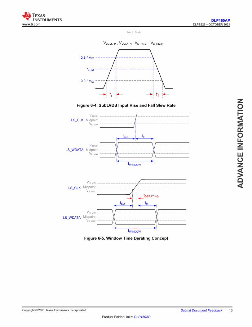
Figure 6-4. SubLVDS Input Rise and Fall Slew Rate
LS_WDATA
LS_CLK
tSU tH
tWINDOW
VIH MIN
VIL MAX
Midpoint
VIH MIN
VIL MAX
Midpoint
tSU tH
tWINDOW
VIH MIN
VIL MAX
Midpoint
VIH MIN
VIL MAX
Midpoint
LS_WDATA
LS_CLK
tDERATING
Figure 6-5. Window Time Derating Concept
www.ti.comDLP160AP
DLPS226 – OCTOBER 2021
AD
VAN
CE
INFO
RM
ATIO
N
Copyright © 2021 Texas Instruments Incorporated Submit Document Feedback 13
Product Folder Links: DLP160AP
Figure 6-6. SubLVDS Switching Parameters
Note: Refer to Section 7.3.3 for details.
Figure 6-7. High-Speed Training Scan Window
Figure 6-8. SubLVDS Voltage Parameters
DLP160APDLPS226 – OCTOBER 2021 www.ti.com
AD
VAN
CE IN
FOR
MATIO
N
14 Submit Document Feedback Copyright © 2021 Texas Instruments Incorporated
Product Folder Links: DLP160AP
VCM VID
VSubLVDS max = VCM max + | 1/2 * VID max|
0.575V
1.225V
VSubLVDS min = VCM min – | 1/2 * VID max |
Figure 6-9. SubLVDS Waveform Parameters
Figure 6-10. SubLVDS Equivalent Input Circuit
VIH
Δ VT
VT+
VT-VIL
LS_WDATA
LS_CLK
Not to Scale
Figure 6-11. LPSDR Input Hysteresis
Stop Start
LS_CLK
LS_WDATA
LS_RDATA
Acknowledge
tPD
Figure 6-12. LPSDR Read Out
www.ti.comDLP160AP
DLPS226 – OCTOBER 2021
AD
VAN
CE
INFO
RM
ATIO
N
Copyright © 2021 Texas Instruments Incorporated Submit Document Feedback 15
Product Folder Links: DLP160AP
CL
Tester ChannelOutput Under Test
Data Sheet Timing Reference Point
Device Pin
See Section 7.3.4 for more information.
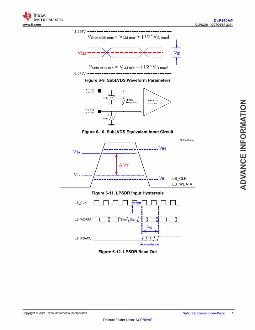
Figure 6-13. Test Load Circuit for Output Propagation Measurement
6.8 Switching Characteristics(1)
Over operating free-air temperature range (unless otherwise noted).PARAMETER TEST CONDITIONS MIN TYP MAX UNIT
tPD
Output propagation, clock to Q, rising edge of LS_CLK input to LS_RDATA output. See Figure 6-12.
CL = 45 pF 15 ns
Slew rate, LS_RDATA 0.5 V/ns
Output duty cycle distortion, LS_RDATA 40% 60%
(1) Device electrical characteristics are over Section 6.4 unless otherwise noted.
DLP160APDLPS226 – OCTOBER 2021 www.ti.com
AD
VAN
CE IN
FOR
MATIO
N
16 Submit Document Feedback Copyright © 2021 Texas Instruments Incorporated
Product Folder Links: DLP160AP
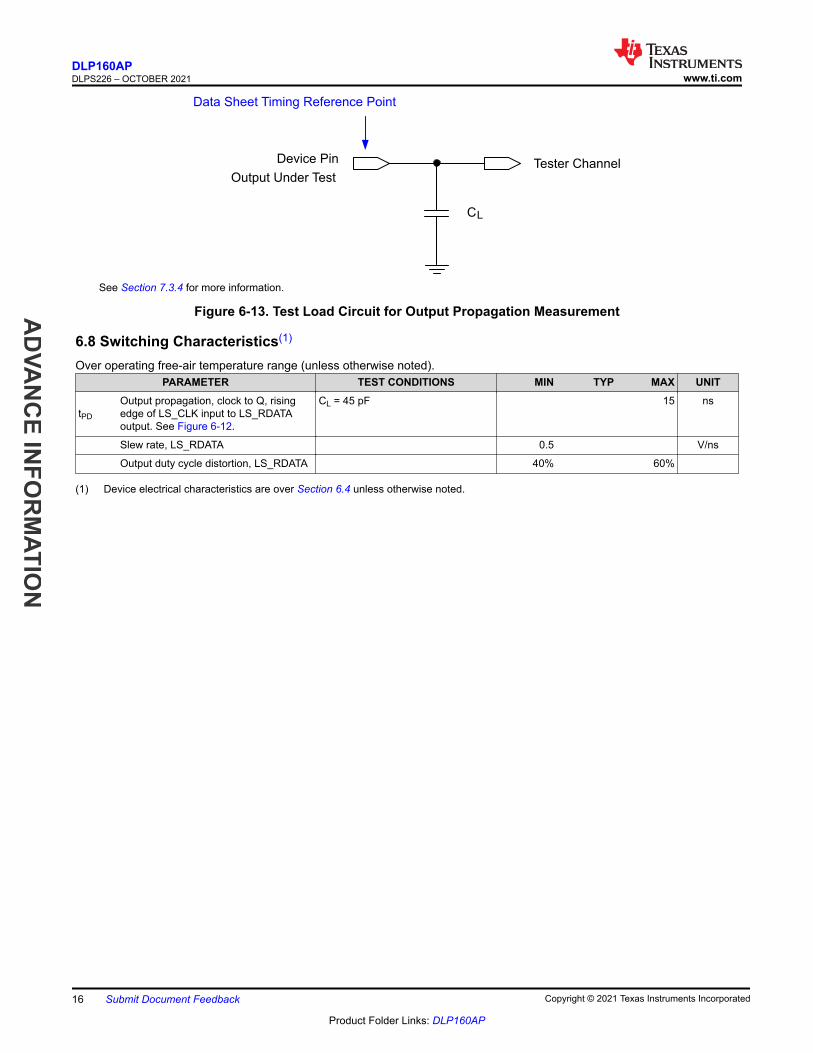
6.9 System Mounting Interface LoadsPARAMETER MIN NOM MAX UNIT
Maximum system mounting interface load to be applied to the:
• Thermal interface area (1) 42 N
• Clamping and electrical interface area (1) 94 N
(1) Uniformly distributed within area shown in Figure 6-14.
Electrical Interface Area
Thermal Interface Area
Figure 6-14. System Interface Loads
www.ti.comDLP160AP
DLPS226 – OCTOBER 2021
AD
VAN
CE
INFO
RM
ATIO
N
Copyright © 2021 Texas Instruments Incorporated Submit Document Feedback 17
Product Folder Links: DLP160AP
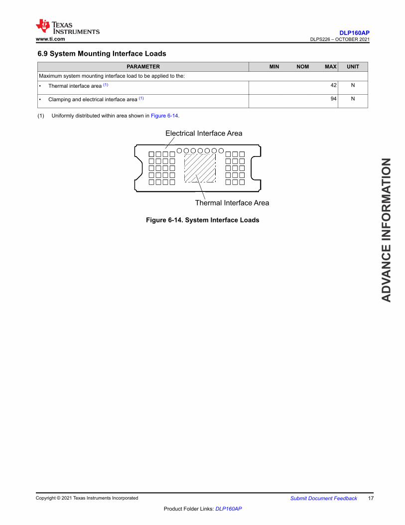
6.10 Micromirror Array Physical CharacteristicsPARAMETER VALUE UNIT
Number of active columns See Figure 6-15 640 (2) micromirrors
Number of active rows See Figure 6-15 360 (2) micromirrors
ε Micromirror (pixel) pitch See Figure 6-16 5.4 µm
Micromirror active array width Micromirror pitch × number of active columns; see Figure 6-15 3.456 mm
Micromirror active array height Micromirror pitch × number of active rows; see Figure 6-15 1.944 mm
Micromirror active border Pond of micromirror (POM)(1) 20 micromirrors/side
(1) The structure and qualities of the border around the active array include a band of partially functional micromirrors called the POM. These micromirrors are structurally or electrically prevented from tilting toward the bright or ON state, but still require an electrical bias to tilt toward OFF.
(2) The DLP image processing in the DMD combined with limited input resolution for this chipset result in a 320 x 180 image resolution being displayed.
DMD active mirror array
640 mirrors x 360 mirrors
359
358357
637
638
6390 1 2 3
3
210
Incident
Illumination
light path
3.456 mm
1.9
44 m
m
Not to scale
Figure 6-15. Micromirror Array Physical Characteristics
ε
ε
εε
Figure 6-16. Mirror (Pixel) Pitch
DLP160APDLPS226 – OCTOBER 2021 www.ti.com
AD
VAN
CE IN
FOR
MATIO
N
18 Submit Document Feedback Copyright © 2021 Texas Instruments Incorporated
Product Folder Links: DLP160AP
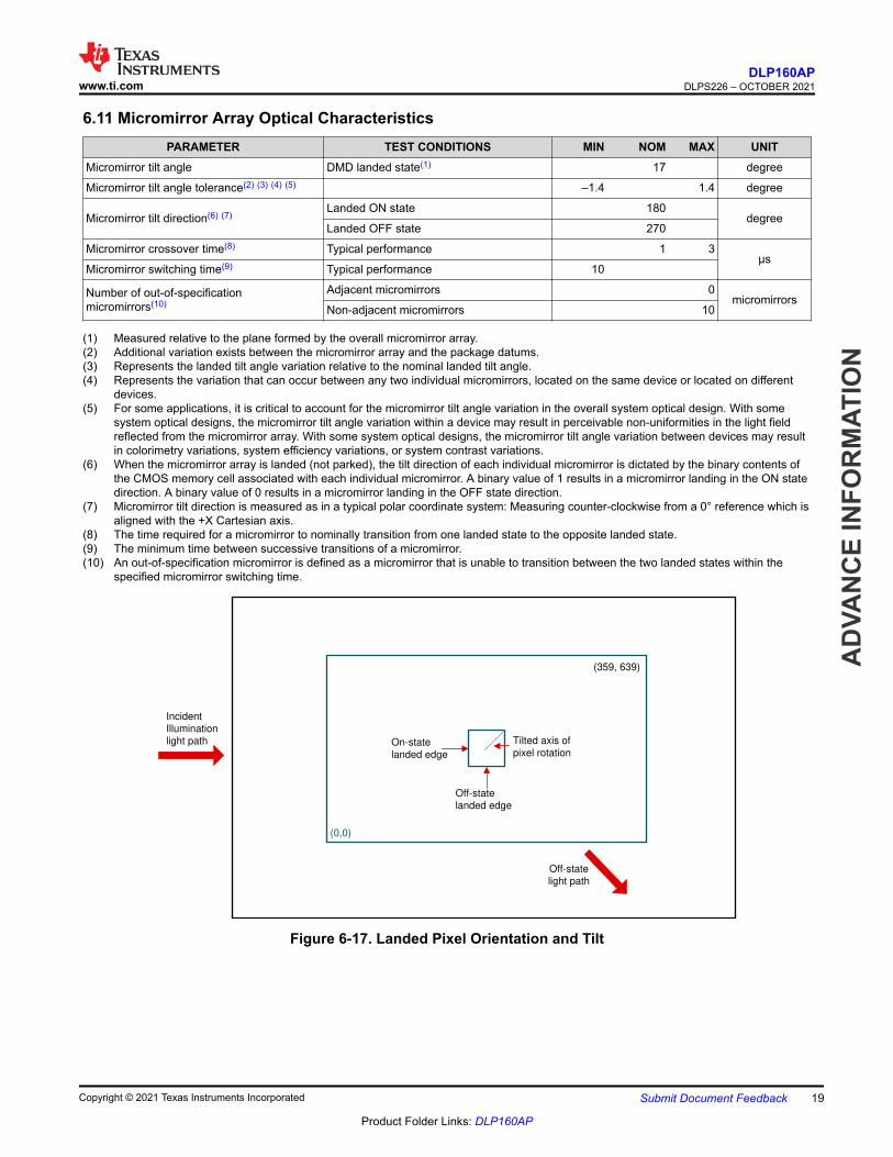
6.11 Micromirror Array Optical CharacteristicsPARAMETER TEST CONDITIONS MIN NOM MAX UNIT
Micromirror tilt angle DMD landed state(1) 17 degree
Micromirror tilt angle tolerance(2) (3) (4) (5) –1.4 1.4 degree
Micromirror tilt direction(6) (7)Landed ON state 180
degreeLanded OFF state 270
Micromirror crossover time(8) Typical performance 1 3µs
Micromirror switching time(9) Typical performance 10
Number of out-of-specification micromirrors(10)
Adjacent micromirrors 0micromirrors
Non-adjacent micromirrors 10
(1) Measured relative to the plane formed by the overall micromirror array.(2) Additional variation exists between the micromirror array and the package datums.(3) Represents the landed tilt angle variation relative to the nominal landed tilt angle.(4) Represents the variation that can occur between any two individual micromirrors, located on the same device or located on different
devices.(5) For some applications, it is critical to account for the micromirror tilt angle variation in the overall system optical design. With some
system optical designs, the micromirror tilt angle variation within a device may result in perceivable non-uniformities in the light field reflected from the micromirror array. With some system optical designs, the micromirror tilt angle variation between devices may result in colorimetry variations, system efficiency variations, or system contrast variations.
(6) When the micromirror array is landed (not parked), the tilt direction of each individual micromirror is dictated by the binary contents of the CMOS memory cell associated with each individual micromirror. A binary value of 1 results in a micromirror landing in the ON state direction. A binary value of 0 results in a micromirror landing in the OFF state direction.
(7) Micromirror tilt direction is measured as in a typical polar coordinate system: Measuring counter-clockwise from a 0° reference which is aligned with the +X Cartesian axis.
(8) The time required for a micromirror to nominally transition from one landed state to the opposite landed state.(9) The minimum time between successive transitions of a micromirror.(10) An out-of-specification micromirror is defined as a micromirror that is unable to transition between the two landed states within the
specified micromirror switching time.
(0,0)
(359, 639)
Incident
Illumination
light path On-state
landed edge
Tilted axis of
pixel rotation
Off-state
landed edge
Off-state
light path
Figure 6-17. Landed Pixel Orientation and Tilt
www.ti.comDLP160AP
DLPS226 – OCTOBER 2021
AD
VAN
CE
INFO
RM
ATIO
N
Copyright © 2021 Texas Instruments Incorporated Submit Document Feedback 19
Product Folder Links: DLP160AP
6.12 Window CharacteristicsPARAMETER(1) MIN NOM MAX UNIT
Window material Corning Eagle XG
Window refractive index At wavelength 546.1 nm 1.5119
Window aperture(2) See (2)
Illumination overfill(3) See (3)
Window transmittance, single-pass through both surfaces and glass
Minimum within the wavelength range 420 to 680 nm. Applies to all angles 0° to 30° AOI.
97%
Average over the wavelength range 420 to 680 nm. Applies to all angles 30° to 45° AOI.
97%
(1) See Section 7.5 for more information.(2) See the package mechanical characteristics for details regarding the size and location of the window aperture.(3) The active area of the device is surrounded by an aperture on the inside of the DMD window surface that masks structures of the
DMD device assembly from normal view. The aperture is sized to anticipate several optical conditions. Overfill light illuminating the area outside the active array can scatter and create adverse effects to the performance of an end application using the DMD. The illumination optical system should be designed to limit light flux incident outside the active array to less than 10% of the average flux level in the active area. Depending on the particular optical architecture and assembly tolerances, the amount of overfill light on the outside of the active array may cause system performance degradation.
6.13 Chipset Component Usage Specification
Note
TI assumes no responsibility for image quality artifacts or DMD failures caused by optical system operating conditions exceeding limits described previously.
The is a component of one or more DLP® chipsets. Reliable function and operation of the requires that it be used in conjunction with the other components of the applicable DLP chipset, including those components that contain or implement TI DMD control technology. TI DMD control technology consists of the TI technology and devices used for operating or controlling a DLP DMD.
DLP160APDLPS226 – OCTOBER 2021 www.ti.com
AD
VAN
CE IN
FOR
MATIO
N
20 Submit Document Feedback Copyright © 2021 Texas Instruments Incorporated
Product Folder Links: DLP160AP
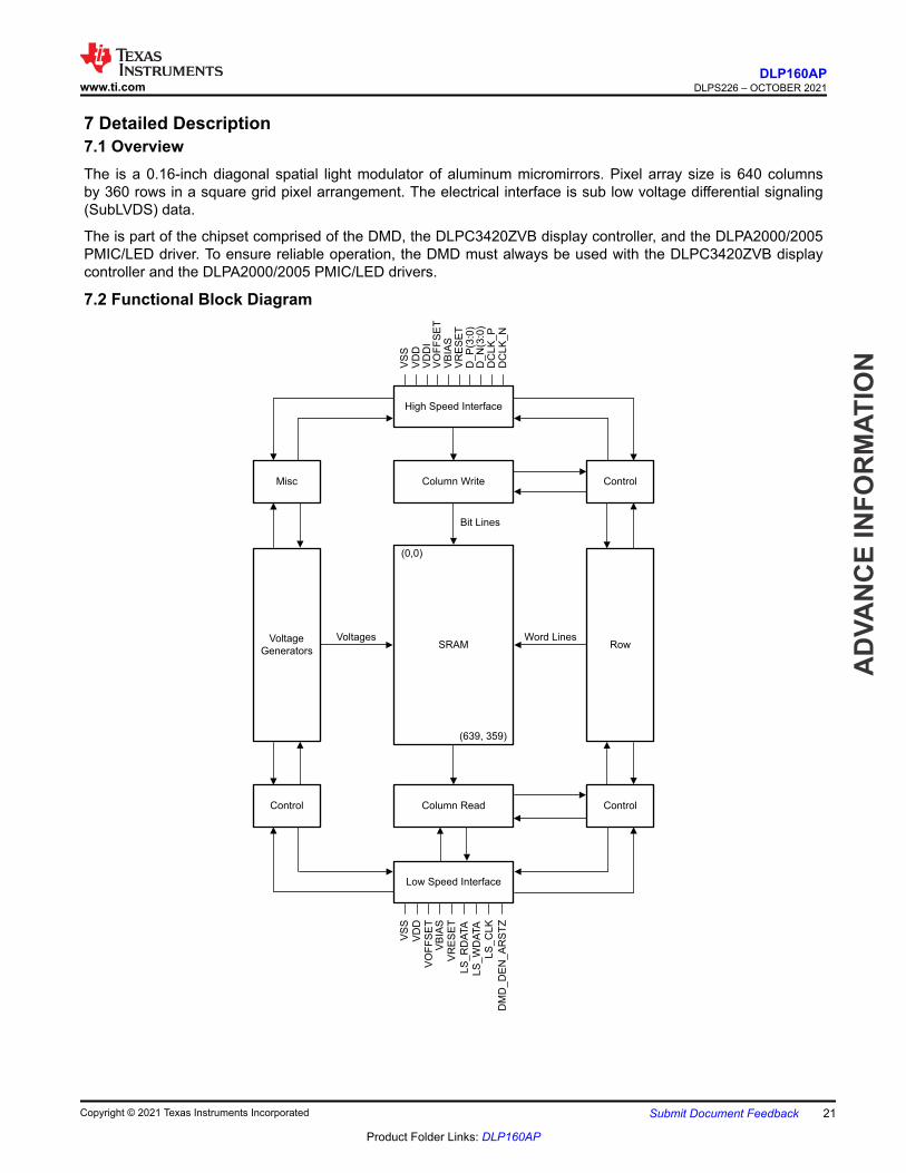
7 Detailed Description7.1 OverviewThe is a 0.16-inch diagonal spatial light modulator of aluminum micromirrors. Pixel array size is 640 columns by 360 rows in a square grid pixel arrangement. The electrical interface is sub low voltage differential signaling (SubLVDS) data.
The is part of the chipset comprised of the DMD, the DLPC3420ZVB display controller, and the DLPA2000/2005 PMIC/LED driver. To ensure reliable operation, the DMD must always be used with the DLPC3420ZVB display controller and the DLPA2000/2005 PMIC/LED drivers.
7.2 Functional Block Diagram
Voltages Word Lines
Bit Lines
VS
SV
DD
VD
DI
VO
FF
SE
TV
BIA
SV
RE
SE
TD
_P
(3:0
)D
_N
(3:0
)D
CLK
_P
DC
LK
_N
VS
S
VD
D
LS
_R
DA
TA
VO
FF
SE
TV
BIA
SV
RE
SE
T
LS
_W
DA
TA
LS
_C
LK
DM
D_D
EN
_A
RS
TZ
SRAMVoltage
GeneratorsRow
Control ControlColumn Read
Low Speed Interface
Misc ControlColumn Write
High Speed Interface
(639, 359)
(0,0)
www.ti.comDLP160AP
DLPS226 – OCTOBER 2021
AD
VAN
CE
INFO
RM
ATIO
N
Copyright © 2021 Texas Instruments Incorporated Submit Document Feedback 21
Product Folder Links: DLP160AP
7.3 Feature Description7.3.1 Power Interface
The power management IC DLPA2000/2005 contains three regulated DC supplies for the DMD reset circuitry: VBIAS, VRESET and VOFFSET, as well as the two regulated DC supplies for the DLPC3420ZVB controller.
7.3.2 Low-Speed Interface
The low speed interface handles instructions that configure the DMD and control reset operation. LS_CLK is the low–speed clock, and LS_WDATA is the low speed data input.
7.3.3 High-Speed Interface
The purpose of the high-speed interface is to transfer pixel data rapidly and efficiently, making use of high speed DDR transfer and compression techniques to save power and time. The high-speed interface is composed of differential SubLVDS receivers for inputs with a dedicated clock.
7.3.4 Timing
The data sheet provides timing at the device pin. For output timing analysis, the tester pin electronics and its transmission line effects must be taken into account. Figure 6-13 shows an equivalent test load circuit for the output under test. Timing reference loads are not intended as a precise representation of any particular system environment or depiction of the actual load presented by a production test. System designers should use IBIS or other simulation tools to correlate the timing reference load to a system environment. The load capacitance value stated is only for characterization and measurement of AC timing signals. This load capacitance value does not indicate the maximum load the device is capable of driving.
7.4 Device Functional ModesDMD functional modes are controlled by the DLPC3420ZVB controller. See the DLPC3420ZVB controller data sheet or contact a TI applications engineer.
7.5 Optical Interface and System Image Quality ConsiderationsTI assumes no responsibility for end-equipment optical performance. Achieving the desired end-equipment optical performance involves making trade-offs between numerous component and system design parameters. Optimizing system optical performance and image quality strongly relate to optical system design parameter trades. Although it is not possible to anticipate every conceivable application, projector image quality and optical performance is contingent on compliance to the optical system operating conditions described in the following sections.
7.5.1 Numerical Aperture and Stray Light Control
The angle defined by the numerical aperture of the illumination and projection optics at the DMD optical area should be the same. This angle should not exceed the nominal device mirror tilt angle unless appropriate apertures are added in the illumination and/or projection pupils to block out flat-state and stray light from the projection lens. The mirror tilt angle defines DMD capability to separate the ON optical path from any other light path, including undesirable flat–state specular reflections from the DMD window, DMD border structures, or other system surfaces near the DMD such as prism or lens surfaces. If the numerical aperture exceeds the mirror tilt angle, or if the projection numerical aperture angle is more than two degrees larger than the illumination numerical aperture angle, objectionable artifacts in the display border and/or active area could occur.
7.5.2 Pupil Match
TI’s optical and image quality specifications assume that the exit pupil of the illumination optics is nominally centered within 2° of the entrance pupil of the projection optics. Misalignment of pupils can create objectionable artifacts in the display border and/or active area, which may require additional system apertures to control, especially if the numerical aperture of the system exceeds the pixel tilt angle.
7.5.3 Illumination Overfill
The active area of the device is surrounded by an aperture on the inside DMD window surface that masks structures of the DMD chip assembly from normal view and is sized to anticipate several optical operating
DLP160APDLPS226 – OCTOBER 2021 www.ti.com
AD
VAN
CE IN
FOR
MATIO
N
22 Submit Document Feedback Copyright © 2021 Texas Instruments Incorporated
Product Folder Links: DLP160AP
conditions. Overfill light illuminating the window aperture can create artifacts from the edge of the window aperture opening and other surface anomalies that may be visible on the screen. The illumination optical system should be designed to limit light flux incident anywhere on the window aperture from exceeding approximately 10% of the average flux level in the active area. Depending on the particular optical architecture, overfill light may have to be further reduced below the suggested 10% level in order to be acceptable.
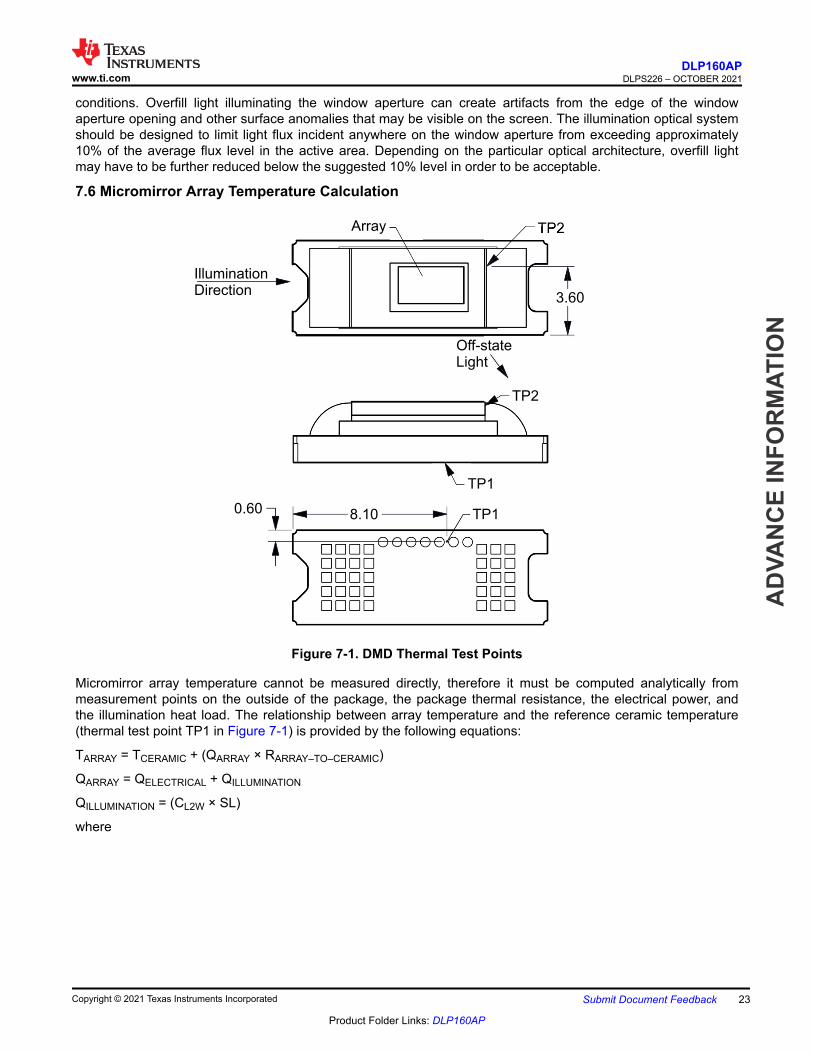
7.6 Micromirror Array Temperature Calculation
TP2
TP2
TP1
TP18.100.60
Array
IlluminationDirection
Off-stateLight
3.60
Figure 7-1. DMD Thermal Test Points
Micromirror array temperature cannot be measured directly, therefore it must be computed analytically from measurement points on the outside of the package, the package thermal resistance, the electrical power, and the illumination heat load. The relationship between array temperature and the reference ceramic temperature (thermal test point TP1 in Figure 7-1) is provided by the following equations:
TARRAY = TCERAMIC + (QARRAY × RARRAY–TO–CERAMIC)
QARRAY = QELECTRICAL + QILLUMINATION
QILLUMINATION = (CL2W × SL)
where
www.ti.comDLP160AP
DLPS226 – OCTOBER 2021
AD
VAN
CE
INFO
RM
ATIO
N
Copyright © 2021 Texas Instruments Incorporated Submit Document Feedback 23
Product Folder Links: DLP160AP
• TARRAY = Computed DMD array temperature (°C)• TCERAMIC = Measured ceramic temperature (°C), TP1 location in Figure 7-1• RARRAY–TO–CERAMIC = Thermal resistance from array to TP1 on ceramic (°C/W) specified in Section 6.5• QARRAY = Total (electrical + absorbed) DMD power on array (W)• QELECTRICAL = Nominal DMD electrical power dissipation (W)• CL2W = Conversion constant for screen lumens to absorbed optical power on the DMD (W/lm) specified below• SL = Measured ANSI screen lumens (lm)
Electrical power dissipation of the DMD is variable and depends on the voltages, data rates, and operating frequencies. Nominal electrical power dissipation to use when calculating array temperature is 0.7 W. Absorbed optical power from the illumination source is variable and depends on the operating state of the micromirrors and the intensity of the light source. Equations shown above are valid for a 1-chip DMD system with total projection efficiency through the projection lens from DMD to the screen of 87%.
The conversion constant CL2W is based on the DMD micromirror array characteristics. It assumes a spectral efficiency of 300 lm/W for the projected light and illumination distribution of 83.7% on the DMD active array, and 16.3% on the DMD array border and window aperture. The conversion constant is calculated to be 0.00266 W/lm.
Sample calculations for typical projection application:
TCERAMIC = 55°C (measured)
SL = 100 lm (measured)
QELECTRICAL = 0.07 W
CL2W = 0.00266 W/lm
QARRAY = 0.07 W + (0.00266 W/lm × 100 lm) = 0.336 W
TARRAY = 55°C + (0.336 W × 13.0°C/W) = 59.4°C
7.7 Micromirror Landed-On/Landed-Off Duty Cycle7.7.1 Definition of Micromirror Landed-On/Landed-Off Duty Cycle
The micromirror landed-on/landed-off duty cycle (landed duty cycle) denotes the amount of time (as a percentage) that an individual micromirror is landed in the ON state versus the amount of time the same micromirror is landed in the OFF state.
As an example, a landed duty cycle of 100/0 indicates that the referenced pixel is in the ON state 100% of the time (and in the OFF state 0% of the time), whereas 0/100 would indicate that the pixel is in the OFF state 100% of the time. Likewise, 50/50 indicates that the pixel is ON 50% of the time and OFF 50% of the time.
Note that when assessing landed duty cycle, the time spent switching from one state (ON or OFF) to the other state (OFF or ON) is considered negligible and is thus ignored.
Since a micromirror can only be landed in one state or the other (ON or OFF), the two numbers (percentages) always add to 100.
7.7.2 Landed Duty Cycle and Useful Life of the DMD
Knowing the long-term average landed duty cycle (of the end product or application) is important because subjecting all (or a portion) of the DMD micromirror array (also called the active array) to an asymmetric landed duty cycle for a prolonged period of time can reduce the usable life of the DMD.
Note that it is the symmetry/asymmetry of the landed duty cycle that is of relevance. The symmetry of the landed duty cycle is determined by how close the two numbers (percentages) are to being equal. For example, a landed duty cycle of 50/50 is perfectly symmetrical whereas a landed duty cycle of 100/0 or 0/100 is perfectly asymmetrical.
DLP160APDLPS226 – OCTOBER 2021 www.ti.com
AD
VAN
CE IN
FOR
MATIO
N
24 Submit Document Feedback Copyright © 2021 Texas Instruments Incorporated
Product Folder Links: DLP160AP
7.7.3 Landed Duty Cycle and Operational DMD Temperature
Operational DMD temperature and landed duty cycle interact to affect the usable life of the DMD, and this interaction can be exploited to reduce the impact that an asymmetrical landed duty cycle has on the usable life of the DMD. This is quantified in the de-rating curve shown in Figure 6-1. The importance of this curve is that:
• All points along this curve represent the same usable life.• All points above this curve represent lower usable life (and the further away from the curve, the lower the
usable life).• All points below this curve represent higher usable life (and the further away from the curve, the higher the
usable life).
In practice, this curve specifies the maximum operating DMD temperature that the DMD should be operated at for a given long-term average landed duty cycle.
7.7.4 Estimating the Long-Term Average Landed Duty Cycle of a Product or Application
During a given period of time, the landed duty cycle of a given pixel follows from the image content being displayed by that pixel.
For example, in the simplest case, when displaying pure-white on a given pixel for a given time period, that pixel will experience close to a 100/0 landed duty cycle during that time period. Likewise, when displaying pure-black, the pixel will experience close to a 0/100 landed duty cycle.
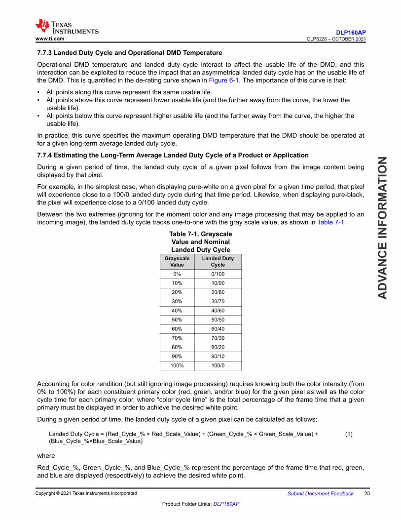
Between the two extremes (ignoring for the moment color and any image processing that may be applied to an incoming image), the landed duty cycle tracks one-to-one with the gray scale value, as shown in Table 7-1.
Table 7-1. Grayscale Value and Nominal Landed Duty Cycle
Grayscale Value
Landed Duty Cycle
0% 0/100
10% 10/90
20% 20/80
30% 30/70
40% 40/60
50% 50/50
60% 60/40
70% 70/30
80% 80/20
90% 90/10
100% 100/0
Accounting for color rendition (but still ignoring image processing) requires knowing both the color intensity (from 0% to 100%) for each constituent primary color (red, green, and/or blue) for the given pixel as well as the color cycle time for each primary color, where “color cycle time” is the total percentage of the frame time that a given primary must be displayed in order to achieve the desired white point.
During a given period of time, the landed duty cycle of a given pixel can be calculated as follows:
Landed Duty Cycle = (Red_Cycle_% × Red_Scale_Value) + (Green_Cycle_% × Green_Scale_Value) + (Blue_Cycle_%×Blue_Scale_Value)
(1)
where
Red_Cycle_%, Green_Cycle_%, and Blue_Cycle_% represent the percentage of the frame time that red, green, and blue are displayed (respectively) to achieve the desired white point.
www.ti.comDLP160AP
DLPS226 – OCTOBER 2021
AD
VAN
CE
INFO
RM
ATIO
N
Copyright © 2021 Texas Instruments Incorporated Submit Document Feedback 25
Product Folder Links: DLP160AP
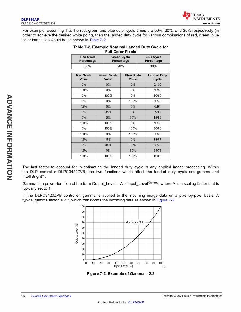
For example, assuming that the red, green and blue color cycle times are 50%, 20%, and 30% respectively (in order to achieve the desired white point), then the landed duty cycle for various combinations of red, green, blue color intensities would be as shown in Table 7-2.
Table 7-2. Example Nominal Landed Duty Cycle for Full-Color Pixels
Red Cycle Percentage
Green Cycle Percentage
Blue Cycle Percentage
50% 20% 30%
Red Scale Value
Green Scale Value
Blue Scale Value
Landed Duty Cycle
0% 0% 0% 0/100
100% 0% 0% 50/50
0% 100% 0% 20/80
0% 0% 100% 30/70
12% 0% 0% 6/94
0% 35% 0% 7/93
0% 0% 60% 18/82
100% 100% 0% 70/30
0% 100% 100% 50/50
100% 0% 100% 80/20
12% 35% 0% 13/87
0% 35% 60% 25/75
12% 0% 60% 24/76
100% 100% 100% 100/0
The last factor to account for in estimating the landed duty cycle is any applied image processing. Within the DLP controller DLPC3420ZVB, the two functions which affect the landed duty cycle are gamma and IntelliBright™.
Gamma is a power function of the form Output_Level = A × Input_LevelGamma, where A is a scaling factor that is typically set to 1.
In the DLPC3420ZVB controller, gamma is applied to the incoming image data on a pixel-by-pixel basis. A typical gamma factor is 2.2, which transforms the incoming data as shown in Figure 7-2.
Input Level (%)
Outp
ut
Level (%
)
0 10 20 30 40 50 60 70 80 90 1000
10
20
30
40
50
60
70
80
90
100
D002
Gamma = 2.2
Figure 7-2. Example of Gamma = 2.2
DLP160APDLPS226 – OCTOBER 2021 www.ti.com
AD
VAN
CE IN
FOR
MATIO
N
26 Submit Document Feedback Copyright © 2021 Texas Instruments Incorporated
Product Folder Links: DLP160AP

From Figure 7-2, if the gray scale value of a given input pixel is 40% (before gamma is applied), then gray scale value will be 13% after gamma is applied. Therefore, it can be seen that since gamma has a direct impact displayed gray scale level of a pixel, it also has a direct impact on the landed duty cycle of a pixel.
The content adaptive illumination control (CAIC) and local area brightness boost (LABB) of the IntelliBright algorithm also apply transform functions on the gray scale level of each pixel.
But while the amount of gamma applied to every pixel of every frame is constant (the exponent, gamma, is constant), CAIC and LABB are both adaptive functions that can apply different amounts of either boost or compression to every pixel of every frame.
Consideration must also be given to any image processing which occurs before the DLPC3420ZVB controller.
www.ti.comDLP160AP
DLPS226 – OCTOBER 2021
AD
VAN
CE
INFO
RM
ATIO
N
Copyright © 2021 Texas Instruments Incorporated Submit Document Feedback 27
Product Folder Links: DLP160AP
8 Application and ImplementationNote
Information in the following applications sections is not part of the TI component specification, and TI does not warrant its accuracy or completeness. TI’s customers are responsible for determining suitability of components for their purposes, as well as validating and testing their design implementation to confirm system functionality.
8.1 Application InformationThe DMDs are spatial light modulators which reflect incoming light from an illumination source to one of two directions, with the primary direction being into a projection or collection optic. Each application is derived primarily from the optical architecture of the system and the format of the data coming into the DLPC3420 controller. The new high tilt pixel in the side-illuminated DMD increases brightness performance and enables a smaller system footprint for thickness-constrained applications. Applications of interest include projection technology embedded in display devices like ultra low-power battery operated mobile accessory projectors, phones, tablets, ultra-mobile low-end Smart TVs, and virtual assistants.
DMD power-up and power-down sequencing is strictly controlled by the DLPA2000/2005. Refer to Section 9 for power-up and power-down specifications. To ensure reliable operation, the DMD must always be used with the DLPC3420 display controller and a DLPA2000/2005 PMIC/LED driver.
DLP160APDLPS226 – OCTOBER 2021 www.ti.com
AD
VAN
CE IN
FOR
MATIO
N
28 Submit Document Feedback Copyright © 2021 Texas Instruments Incorporated
Product Folder Links: DLP160AP
8.2 Typical ApplicationA common application when using a DMD and a DLPC3420 is for creating a pico projector that can be used as an accessory to a smartphone, tablet, or a laptop. The DLPC3420 in the pico projector receives images from a multimedia front end within the product as shown in Figure 8-1.
Projector Module Electronics
DC Supplies
BAT+ ±
1.0 V
WVGADDR DMD0.16 QnHD
L1
Included in DLP® Chip Set along with DMD
3
DLPC3420
L2
1.8 V
CLRL
DATA
2.3 V - 5.5 V
Connector
Flash
BIAS, RST, OFS
Thermistor
½ Bus sub-LVDS
RGB
PAD2000
PWR_EN
Parallel or BT.656
Host
Processor
1.0 V1.8 V
VCOREVIO
IlluminationOptic
L5
L6
DualReg.
GPIO4
GPIO5
PARKZ
CTRL
DATA
RED
GREEN
BLUESPI(4)
LED_SEL(2)
PWM_IN
CMP_OUT
INTZ
RESETZ
SYSPWR
PROJ_ON
PROJ_ON
INIT_DONE
4
2824/16/8
I2C
VLED
Figure 8-1. Typical Application Diagram
8.2.1 Design Requirements
A pico projector is created by using a DLP chipset comprised of a DMD, a DLPC3420 controller, and a DLPA2000/2005 PMIC/LED driver. The DLPC3420 controller performs the digital image processing, the DLPA2000/2005 provides the needed analog functions for the projector, and the DMD is the display device for producing the projected image.
In addition to the three DLP chips in the chipset, other chips are needed. At a minimum a flash part is needed to store the DLPC3420 controller software.
The illumination light that is applied to the DMD is typically from red, green, and blue LEDs. These are often contained in three separate packages, but sometimes more than one color of LED die may be in the same package to reduce the overall size of the pico projector.
The DLPC3420 controller receives image data from the multimedia front end over a 24-bit parallel interface. An I2C interface should be connected from the multimedia front end for sending commands to the DLPC3420 controller for configuring the chipset for different features.
8.2.2 Detailed Design Procedure
For instructions on how to connect the DLPC3420 controller, the DLPA2000/2005, and the DMD together, see the reference design schematic. When a circuit board layout is created from this schematic a very small circuit board is possible. An example small board layout is included in the reference design data base. Layout guidelines should be followed to achieve a reliable projector.
The optical engine that has the LED packages and the DMD mounted to it is typically supplied by an optical OEM who specializes in designing optics for DLP projectors.
www.ti.comDLP160AP
DLPS226 – OCTOBER 2021
AD
VAN
CE
INFO
RM
ATIO
N
Copyright © 2021 Texas Instruments Incorporated Submit Document Feedback 29
Product Folder Links: DLP160AP
8.2.3 Application Curve
As the LED currents that are driven time-sequentially through the red, green, and blue LEDs are increased, the brightness of the projector increases. This increase is somewhat non-linear, and the curve for typical white screen lumens changes with LED currents is as shown in Figure 8-2. For the LED currents shown, it is assumed that the same current amplitude is applied to the red, green, and blue LEDs.
Current (mA)
Lu
min
an
ce
0 500 1000 1500 2000 2500 30000
0.1
0.2
0.3
0.4
0.5
0.6
0.7
0.8
0.9
1
D001
Figure 8-2. Luminance vs Current
DLP160APDLPS226 – OCTOBER 2021 www.ti.com
AD
VAN
CE IN
FOR
MATIO
N
30 Submit Document Feedback Copyright © 2021 Texas Instruments Incorporated
Product Folder Links: DLP160AP
9 Power Supply RecommendationsThe following power supplies are all required to operate the DMD: VDD, VDDI, VOFFSET, VBIAS, and VRESET. All VSS connections are also required. DMD power-up and power-down sequencing is strictly controlled by the DLPA2000/2005 devices.
CAUTION
For reliable operation of the DMD, the following power supply sequencing requirements must be followed. Failure to adhere to the prescribed power-up and power-down procedures may affect device reliability.
VDD, VDDI, VOFFSET, VBIAS, and VRESET power supplies have to be coordinated during power-up and power-down operations. Failure to meet any of the below requirements will result in a significant reduction in the reliability and lifetime of the DMD. Refer to Figure 9-2. VSS must also be connected.
9.1 Power Supply Power-Up Procedure• During power-up, VDD and VDDI must always start and settle before VOFFSET, VBIAS, and VRESET voltages are
applied to the DMD.• During power-up, it is a strict requirement that the delta between VBIAS and VOFFSET must be within the
specified limit shown in Section 6.4. Refer to Figure 9-2 for power-up delay requirements.• During power-up, the LPSDR input pins of the DMD shall not be driven high until after VDD and VDDI have
settled at operating voltage.• During power-up, there is no requirement for the relative timing of VRESET with respect to VOFFSET and VBIAS.
Power supply slew rates during power-up are flexible, provided that the transient voltage levels follow the requirements listed previously and in Figure 9-1.
9.2 Power Supply Power-Down Procedure• The power-down sequence is the reverse order of the previous power-up sequence. VDD and VDDI must be
supplied until after VBIAS, VRESET, and VOFFSET are discharged to within 4 V of ground.• During power-down, it is not mandatory to stop driving VBIAS prior to VOFFSET, but it is a strict requirement that
the delta between VBIAS and VOFFSET must be within the specified limit shown in Section 6.4 (Refer to Note 2 for Figure 9-1).
• During power-down, the LPSDR input pins of the DMD must be less than VDDI, the specified limit shown in Section 6.4.
• During power-down, there is no requirement for the relative timing of VRESET with respect to VOFFSET and VBIAS.
• Power supply slew rates during power-down are flexible, provided that the transient voltage levels follow the requirements listed previously and in Figure 9-1.
www.ti.comDLP160AP
DLPS226 – OCTOBER 2021
AD
VAN
CE
INFO
RM
ATIO
N
Copyright © 2021 Texas Instruments Incorporated Submit Document Feedback 31
Product Folder Links: DLP160AP
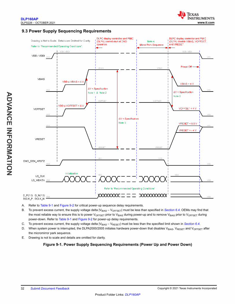
9.3 Power Supply Sequencing Requirements
A. Refer to Table 9-1 and Figure 9-2 for critical power-up sequence delay requirements.B. To prevent excess current, the supply voltage delta |VBIAS – VOFFSET| must be less than specified in Section 6.4. OEMs may find that
the most reliable way to ensure this is to power VOFFSET prior to VBIAS during power-up and to remove VBIAS prior to VOFFSET during power-down. Refer to Table 9-1 and Figure 9-2 for power-up delay requirements.
C. To prevent excess current, the supply voltage delta |VBIAS – VRESET| must be less than the specified limit shown in Section 6.4.D. When system power is interrupted, the DLPA2000/2005 initiates hardware power-down that disables VBIAS, VRESET and VOFFSET after
the micromirror park sequence.E. Drawing is not to scale and details are omitted for clarity.
Figure 9-1. Power Supply Sequencing Requirements (Power Up and Power Down)
DLP160APDLPS226 – OCTOBER 2021 www.ti.com
AD
VAN
CE IN
FOR
MATIO
N
32 Submit Document Feedback Copyright © 2021 Texas Instruments Incorporated
Product Folder Links: DLP160AP
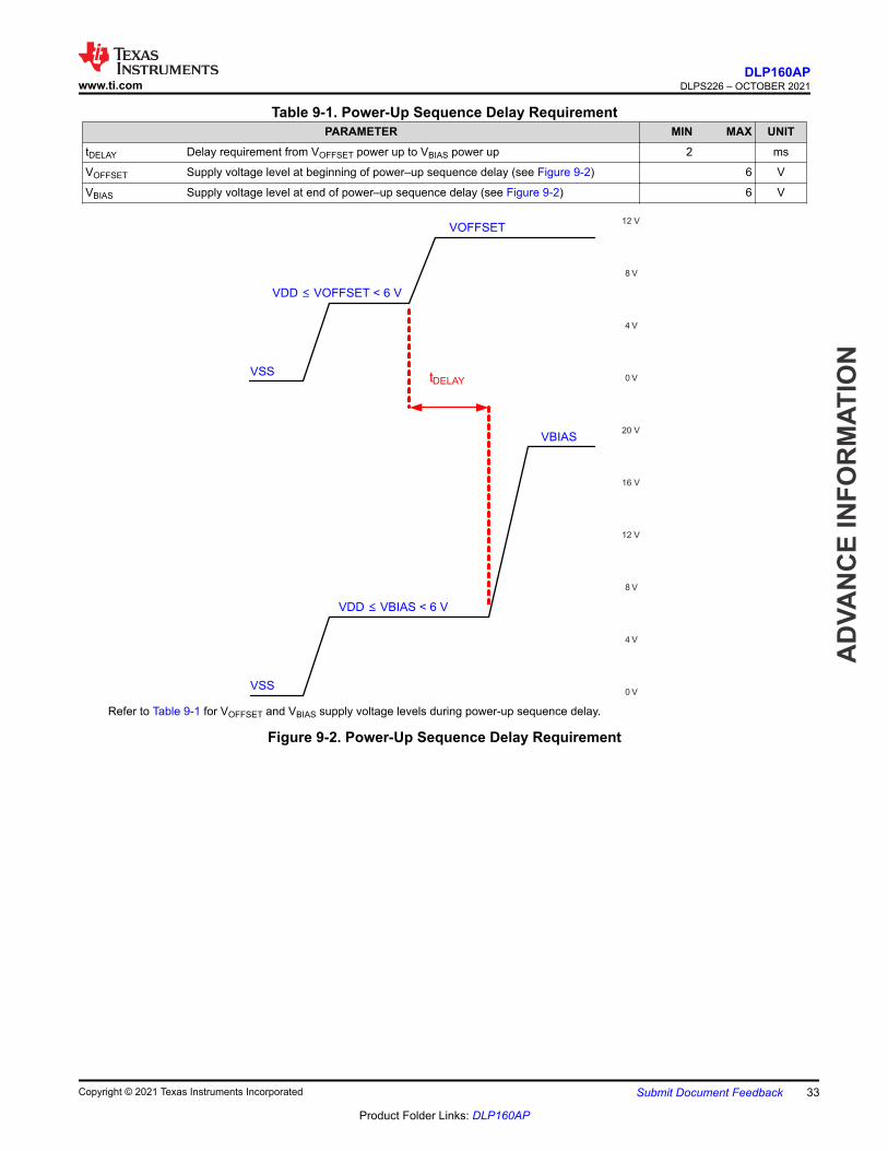
Table 9-1. Power-Up Sequence Delay RequirementPARAMETER MIN MAX UNIT
tDELAY Delay requirement from VOFFSET power up to VBIAS power up 2 ms
VOFFSET Supply voltage level at beginning of power–up sequence delay (see Figure 9-2) 6 V
VBIAS Supply voltage level at end of power–up sequence delay (see Figure 9-2) 6 V
VOFFSET
VBIAS
VSS
VDD VOFFSET≤ < 6 V
VDD VBIAS≤ < 6 V
VSS
tDELAY
20 V
16 V
12 V
8 V
4 V
0 V
12 V
8 V
4 V
0 V
Refer to Table 9-1 for VOFFSET and VBIAS supply voltage levels during power-up sequence delay.
Figure 9-2. Power-Up Sequence Delay Requirement
www.ti.comDLP160AP
DLPS226 – OCTOBER 2021
AD
VAN
CE
INFO
RM
ATIO
N
Copyright © 2021 Texas Instruments Incorporated Submit Document Feedback 33
Product Folder Links: DLP160AP
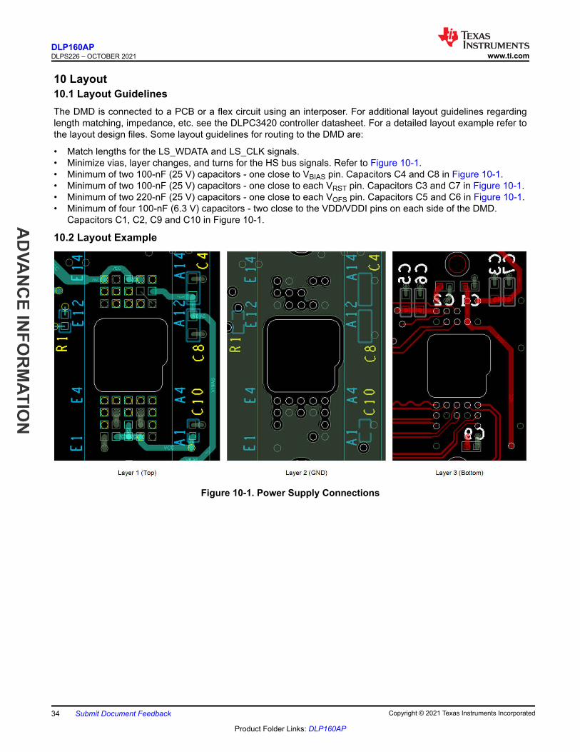
10 Layout10.1 Layout GuidelinesThe DMD is connected to a PCB or a flex circuit using an interposer. For additional layout guidelines regarding length matching, impedance, etc. see the DLPC3420 controller datasheet. For a detailed layout example refer to the layout design files. Some layout guidelines for routing to the DMD are:
• Match lengths for the LS_WDATA and LS_CLK signals.• Minimize vias, layer changes, and turns for the HS bus signals. Refer to Figure 10-1.• Minimum of two 100-nF (25 V) capacitors - one close to VBIAS pin. Capacitors C4 and C8 in Figure 10-1.• Minimum of two 100-nF (25 V) capacitors - one close to each VRST pin. Capacitors C3 and C7 in Figure 10-1.• Minimum of two 220-nF (25 V) capacitors - one close to each VOFS pin. Capacitors C5 and C6 in Figure 10-1.• Minimum of four 100-nF (6.3 V) capacitors - two close to the VDD/VDDI pins on each side of the DMD.
Capacitors C1, C2, C9 and C10 in Figure 10-1.
10.2 Layout Example
Figure 10-1. Power Supply Connections
DLP160APDLPS226 – OCTOBER 2021 www.ti.com
AD
VAN
CE IN
FOR
MATIO
N
34 Submit Document Feedback Copyright © 2021 Texas Instruments Incorporated
Product Folder Links: DLP160AP
11 Device and Documentation Support11.1 Device Support11.1.1 Device Nomenclature
Package Type
Device Descriptor
DLP160AP FQT
Figure 11-1. Part Number Description
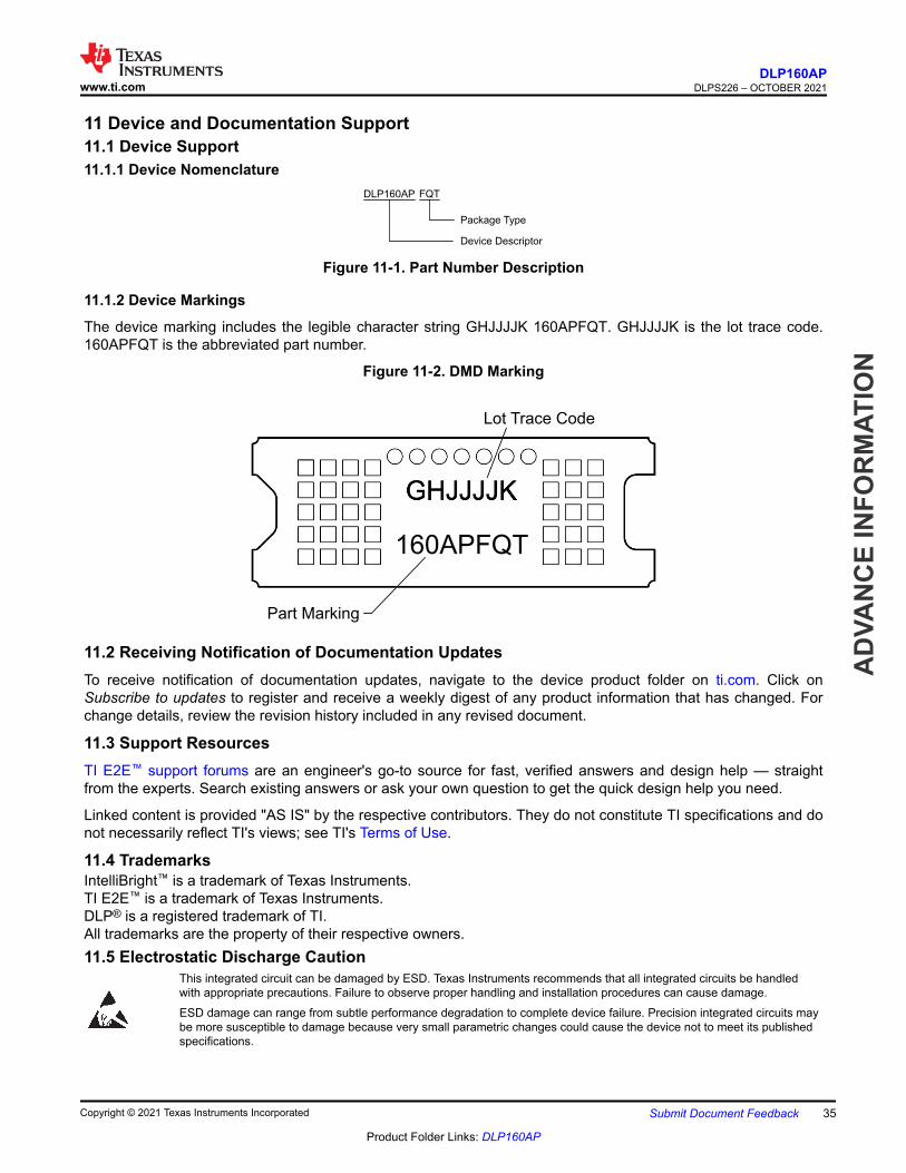
11.1.2 Device Markings
The device marking includes the legible character string GHJJJJK 160APFQT. GHJJJJK is the lot trace code. 160APFQT is the abbreviated part number.
Figure 11-2. DMD Marking
GHJJJJK
Lot Trace Code
Part Marking
160APFQT
11.2 Receiving Notification of Documentation UpdatesTo receive notification of documentation updates, navigate to the device product folder on ti.com. Click on Subscribe to updates to register and receive a weekly digest of any product information that has changed. For change details, review the revision history included in any revised document.
11.3 Support ResourcesTI E2E™ support forums are an engineer's go-to source for fast, verified answers and design help — straight from the experts. Search existing answers or ask your own question to get the quick design help you need.
Linked content is provided "AS IS" by the respective contributors. They do not constitute TI specifications and do not necessarily reflect TI's views; see TI's Terms of Use.
11.4 TrademarksIntelliBright™ is a trademark of Texas Instruments.TI E2E™ is a trademark of Texas Instruments.DLP® is a registered trademark of TI.All trademarks are the property of their respective owners.11.5 Electrostatic Discharge Caution
This integrated circuit can be damaged by ESD. Texas Instruments recommends that all integrated circuits be handled with appropriate precautions. Failure to observe proper handling and installation procedures can cause damage.ESD damage can range from subtle performance degradation to complete device failure. Precision integrated circuits may be more susceptible to damage because very small parametric changes could cause the device not to meet its published specifications.
www.ti.comDLP160AP
DLPS226 – OCTOBER 2021
AD
VAN
CE
INFO
RM
ATIO
N
Copyright © 2021 Texas Instruments Incorporated Submit Document Feedback 35
Product Folder Links: DLP160AP

11.6 GlossaryTI Glossary This glossary lists and explains terms, acronyms, and definitions.
12 Mechanical, Packaging, and Orderable InformationThe following pages include mechanical, packaging, and orderable information. This information is the most current data available for the designated devices. This data is subject to change without notice and revision of this document. For browser-based versions of this data sheet, refer to the left-hand navigation.
DLP160APDLPS226 – OCTOBER 2021 www.ti.com
AD
VAN
CE IN
FOR
MATIO
N
36 Submit Document Feedback Copyright © 2021 Texas Instruments Incorporated
Product Folder Links: DLP160AP
PACKAGE OPTION ADDENDUM
www.ti.com 17-Oct-2021
Addendum-Page 1
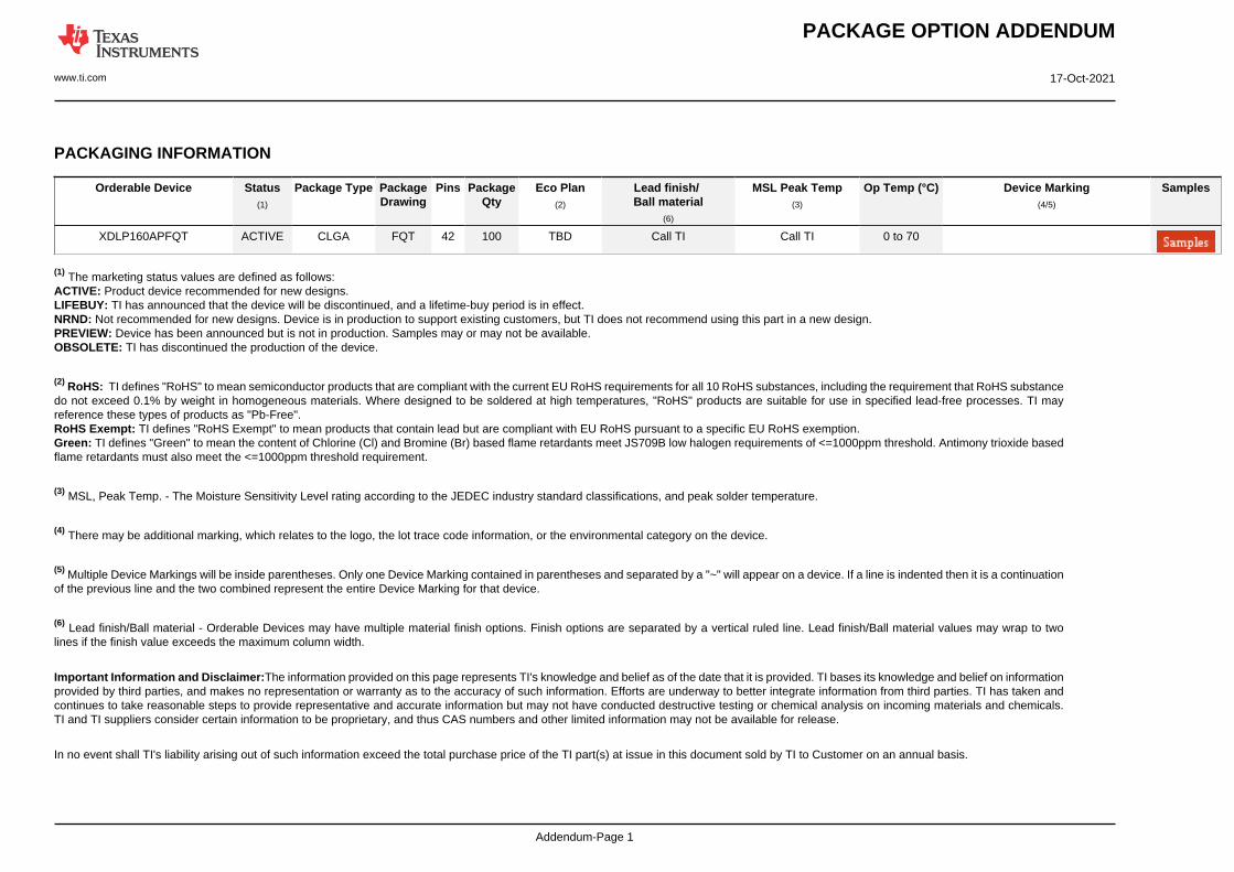
PACKAGING INFORMATION
Orderable Device Status(1)
Package Type PackageDrawing
Pins PackageQty
Eco Plan(2)
Lead finish/Ball material
(6)
MSL Peak Temp(3)
Op Temp (°C) Device Marking(4/5)
Samples
XDLP160APFQT ACTIVE CLGA FQT 42 100 TBD Call TI Call TI 0 to 70
(1) The marketing status values are defined as follows:ACTIVE: Product device recommended for new designs.LIFEBUY: TI has announced that the device will be discontinued, and a lifetime-buy period is in effect.NRND: Not recommended for new designs. Device is in production to support existing customers, but TI does not recommend using this part in a new design.PREVIEW: Device has been announced but is not in production. Samples may or may not be available.OBSOLETE: TI has discontinued the production of the device.
(2) RoHS: TI defines "RoHS" to mean semiconductor products that are compliant with the current EU RoHS requirements for all 10 RoHS substances, including the requirement that RoHS substancedo not exceed 0.1% by weight in homogeneous materials. Where designed to be soldered at high temperatures, "RoHS" products are suitable for use in specified lead-free processes. TI mayreference these types of products as "Pb-Free".RoHS Exempt: TI defines "RoHS Exempt" to mean products that contain lead but are compliant with EU RoHS pursuant to a specific EU RoHS exemption.Green: TI defines "Green" to mean the content of Chlorine (Cl) and Bromine (Br) based flame retardants meet JS709B low halogen requirements of <=1000ppm threshold. Antimony trioxide basedflame retardants must also meet the <=1000ppm threshold requirement.
(3) MSL, Peak Temp. - The Moisture Sensitivity Level rating according to the JEDEC industry standard classifications, and peak solder temperature.
(4) There may be additional marking, which relates to the logo, the lot trace code information, or the environmental category on the device.
(5) Multiple Device Markings will be inside parentheses. Only one Device Marking contained in parentheses and separated by a "~" will appear on a device. If a line is indented then it is a continuationof the previous line and the two combined represent the entire Device Marking for that device.
(6) Lead finish/Ball material - Orderable Devices may have multiple material finish options. Finish options are separated by a vertical ruled line. Lead finish/Ball material values may wrap to twolines if the finish value exceeds the maximum column width.
Important Information and Disclaimer:The information provided on this page represents TI's knowledge and belief as of the date that it is provided. TI bases its knowledge and belief on informationprovided by third parties, and makes no representation or warranty as to the accuracy of such information. Efforts are underway to better integrate information from third parties. TI has taken andcontinues to take reasonable steps to provide representative and accurate information but may not have conducted destructive testing or chemical analysis on incoming materials and chemicals.TI and TI suppliers consider certain information to be proprietary, and thus CAS numbers and other limited information may not be available for release.
In no event shall TI's liability arising out of such information exceed the total purchase price of the TI part(s) at issue in this document sold by TI to Customer on an annual basis.
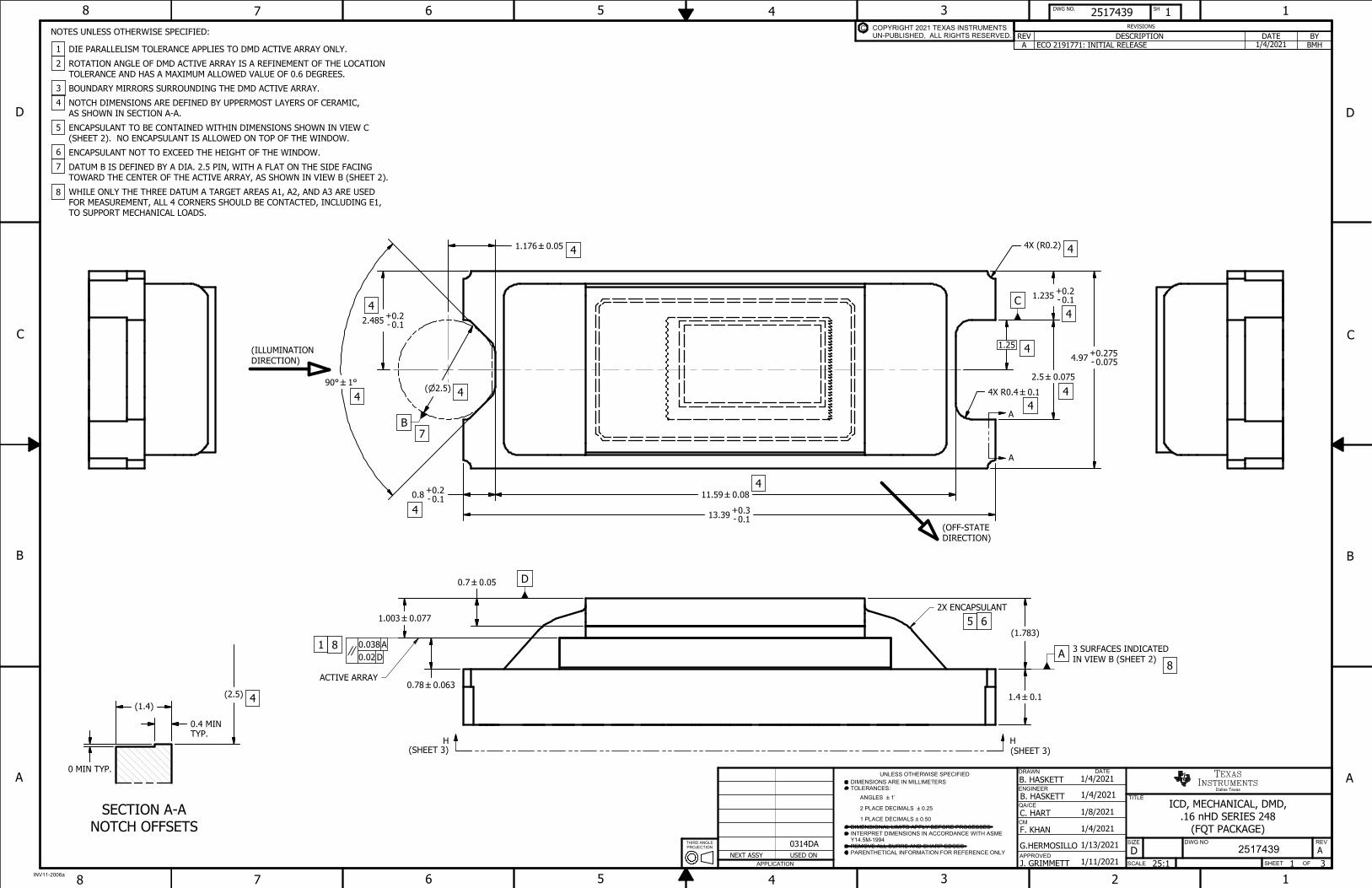
SECTION A-ANOTCH OFFSETS
2 1345678
D
C
B
A
DWG NO. SH8 7 6 5 4 3 1
D
C
B
A
INV11-2006a
2517439 1
TITLE
SIZE DWG NO REV
SCALE SHEET OF
DATE
ENGINEER
QA/CE
CM
APPROVED
DRAWN
INSTRUMENTSDallas Texas
APPLICATIONNEXT ASSY USED ON
THIRD ANGLEPROJECTION
TEXASUNLESS OTHERWISE SPECIFIEDDIMENSIONS ARE IN MILLIMETERSTOLERANCES: ANGLES 1
2 PLACE DECIMALS 0.25
1 PLACE DECIMALS 0.50DIMENSIONAL LIMITS APPLY BEFORE PROCESSESINTERPRET DIMENSIONS IN ACCORDANCE WITH ASME Y14.5M-1994REMOVE ALL BURRS AND SHARP EDGESPARENTHETICAL INFORMATION FOR REFERENCE ONLY
ICD, MECHANICAL, DMD,.16 nHD SERIES 248
(FQT PACKAGE)
25174391 3
AD
1/4/2021
25:1
C. HART
F. KHAN
J. GRIMMETT
1/8/2021
1/4/2021
1/11/2021
1/4/2021
0314DA
B. HASKETT
NOTES UNLESS OTHERWISE SPECIFIED:REVISIONSCOPYRIGHT 2021 TEXAS INSTRUMENTS
UN-PUBLISHED, ALL RIGHTS RESERVED.C
B. HASKETT
G.HERMOSILLO 1/13/2021
A
A
H H
REV DESCRIPTION DATE BYA ECO 2191771: INITIAL RELEASE 1/4/2021 BMH
3 SURFACES INDICATEDIN VIEW B (SHEET 2)
DIE PARALLELISM TOLERANCE APPLIES TO DMD ACTIVE ARRAY ONLY.
ROTATION ANGLE OF DMD ACTIVE ARRAY IS A REFINEMENT OF THE LOCATIONTOLERANCE AND HAS A MAXIMUM ALLOWED VALUE OF 0.6 DEGREES.
BOUNDARY MIRRORS SURROUNDING THE DMD ACTIVE ARRAY.
NOTCH DIMENSIONS ARE DEFINED BY UPPERMOST LAYERS OF CERAMIC,AS SHOWN IN SECTION A-A.
ENCAPSULANT TO BE CONTAINED WITHIN DIMENSIONS SHOWN IN VIEW C(SHEET 2). NO ENCAPSULANT IS ALLOWED ON TOP OF THE WINDOW.
ENCAPSULANT NOT TO EXCEED THE HEIGHT OF THE WINDOW.
DATUM B IS DEFINED BY A DIA. 2.5 PIN, WITH A FLAT ON THE SIDE FACING TOWARD THE CENTER OF THE ACTIVE ARRAY, AS SHOWN IN VIEW B (SHEET 2).
WHILE ONLY THE THREE DATUM A TARGET AREAS A1, A2, AND A3 ARE USEDFOR MEASUREMENT, ALL 4 CORNERS SHOULD BE CONTACTED, INCLUDING E1,TO SUPPORT MECHANICAL LOADS.
1
43
2
76
5
8
(ILLUMINATIONDIRECTION)
(SHEET 3)(SHEET 3)
4
4
4
4
4
4
4
(2.5)
5
8
1
(2.5) 4
B7
4
6
1.1760.05
1.25
C2.485 - 0.1
0.2+
8
90°1°
4.97 - 0.0750.275+
0.8 - 0.10.2+ 11.590.08
13.39 - 0.10.3+
2.50.075
1.235 - 0.10.2+
(R0.2)4X
(OFF-STATEDIRECTION)
4
0.70.05
1.0030.077
0.780.063ACTIVE ARRAY
0.038 A 0.02D
1.40.1
(1.783)
2X ENCAPSULANT
0 MIN TYP.
0.4 MINTYP.
(1.4)
0.4R 0.14X 4
4
A
D
VIEW BDATUMS A, B, C, AND E
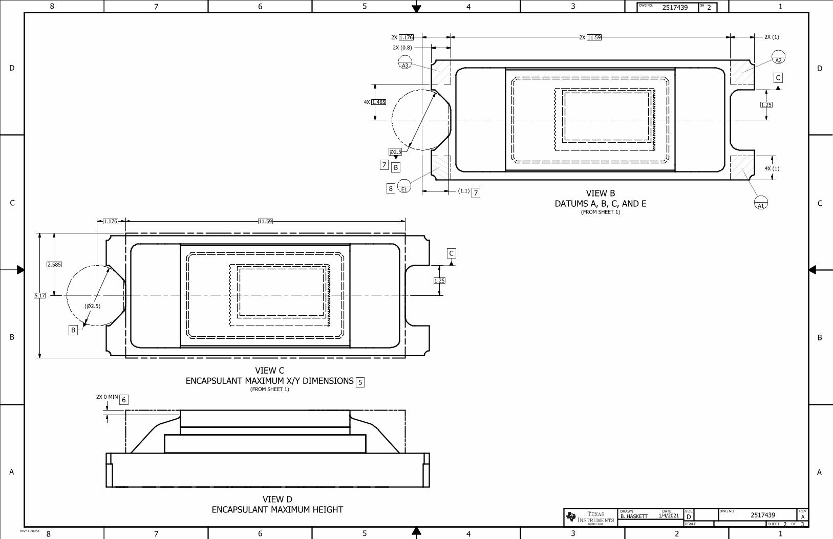
(FROM SHEET 1)
VIEW CENCAPSULANT MAXIMUM X/Y DIMENSIONS
(FROM SHEET 1)
VIEW DENCAPSULANT MAXIMUM HEIGHT
2 1345678
D
C
B
A
DWG NO. SH8 7 6 5 4 3 1
D
C
B
A
INV11-2006a
2517439 2
SIZE DWG NO REV
SCALE SHEET OF
DATE
INSTRUMENTSDallas Texas
TEXASDRAWN
25174392 3
ADB. HASKETT 1/4/2021
1.1762X
(0.8)2X
11.592X (1)2X
(1)4X
2.5
A3A2
A1
E1
B
8 (1.1)
7
(2.5)
B
1.176 11.59
6
5
1.25
C2.585
1.25
C
2X 0 MIN
1.4854X
5.17
7
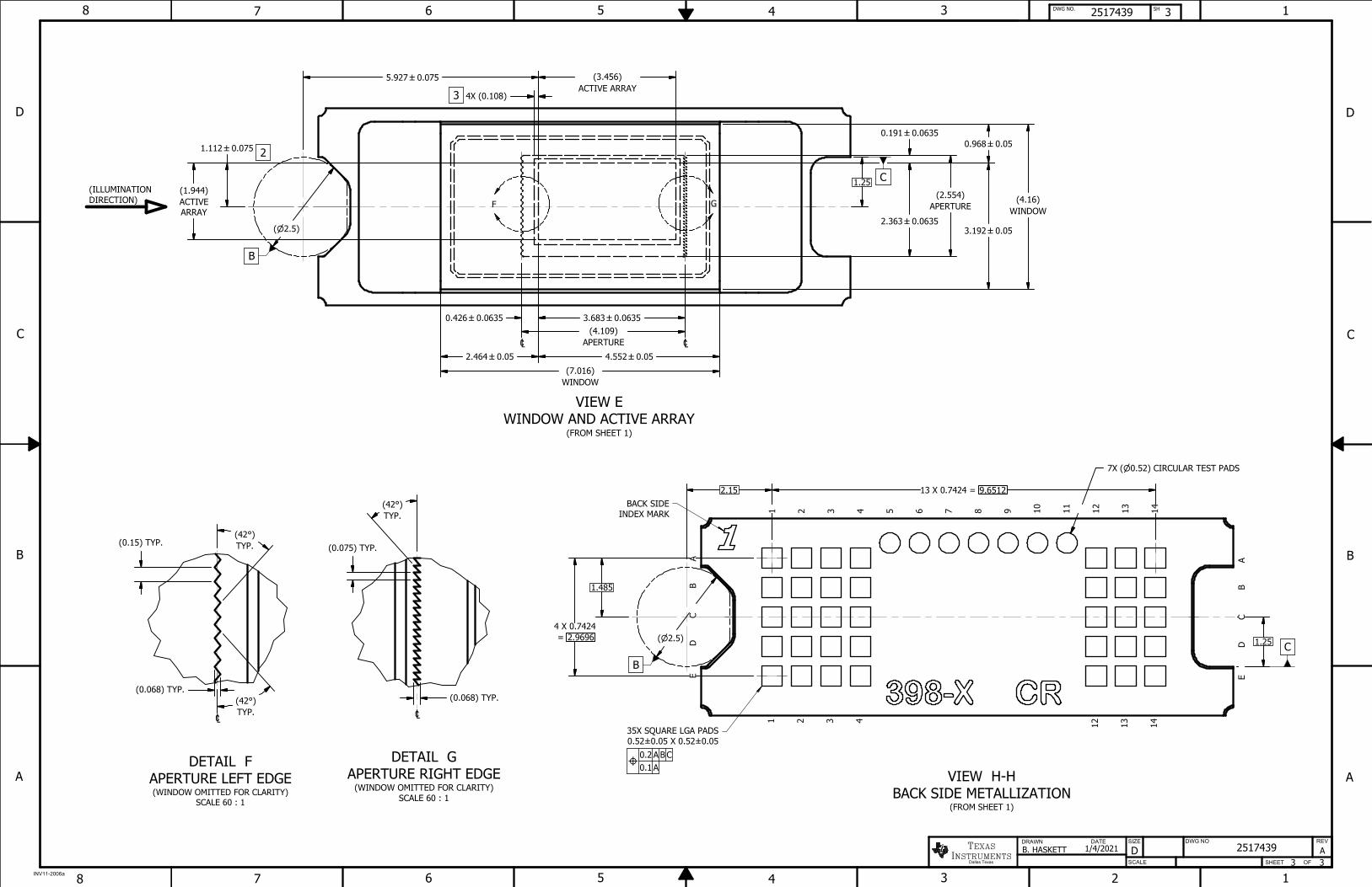
VIEW EWINDOW AND ACTIVE ARRAY
(FROM SHEET 1)
VIEW H-HBACK SIDE METALLIZATION
(FROM SHEET 1)
DETAIL FAPERTURE LEFT EDGE(WINDOW OMITTED FOR CLARITY)
SCALE 60 : 1
DETAIL GAPERTURE RIGHT EDGE
(WINDOW OMITTED FOR CLARITY)SCALE 60 : 1
2 1345678
D
C
B
A
DWG NO. SH8 7 6 5 4 3 1
D
C
B
A
INV11-2006a
2517439 3
SIZE DWG NO REV
SCALE SHEET OF
DATE
INSTRUMENTSDallas Texas
TEXASDRAWN
25174393 3
ADB. HASKETT 1/4/2021
F G
3
2
(2.5)
B
0.2 A B C0.1 A
(ILLUMINATIONDIRECTION)
1.25 C
(3.456)ACTIVE ARRAY
(1.944)ACTIVEARRAY
0.1910.0635
2.3630.0635
(2.554)APERTURE
1.25 C
1.1120.075
5.9270.075
(0.108)4X
(2.5)
B
0.4260.0635 3.6830.0635(4.109)
APERTURE2.4640.05 4.5520.05
(7.016)WINDOW
0.9680.05
3.1920.05
(4.16)WINDOW
1.485
2.9696 = 4 X 0.7424
2.15 9.651213 X 0.7424 =
(0.52)7X CIRCULAR TEST PADS
35X SQUARE LGA PADS0.52±0.05 X 0.52±0.05
BACK SIDEINDEX MARK 1 2 3 4 5 6 7 8 9 10 11 12 13 14
E
D
C
B
A
E
D
C
B
A
1 2 3 4 12 13 14
(42°)TYP.
(42°)TYP.
(0.068) TYP.
(0.15) TYP. (0.075) TYP.
(42°)TYP.
(0.068) TYP.

IMPORTANT NOTICE AND DISCLAIMERTI PROVIDES TECHNICAL AND RELIABILITY DATA (INCLUDING DATA SHEETS), DESIGN RESOURCES (INCLUDING REFERENCE DESIGNS), APPLICATION OR OTHER DESIGN ADVICE, WEB TOOLS, SAFETY INFORMATION, AND OTHER RESOURCES “AS IS” AND WITH ALL FAULTS, AND DISCLAIMS ALL WARRANTIES, EXPRESS AND IMPLIED, INCLUDING WITHOUT LIMITATION ANY IMPLIED WARRANTIES OF MERCHANTABILITY, FITNESS FOR A PARTICULAR PURPOSE OR NON-INFRINGEMENT OF THIRD PARTY INTELLECTUAL PROPERTY RIGHTS.These resources are intended for skilled developers designing with TI products. You are solely responsible for (1) selecting the appropriate TI products for your application, (2) designing, validating and testing your application, and (3) ensuring your application meets applicable standards, and any other safety, security, regulatory or other requirements.These resources are subject to change without notice. TI grants you permission to use these resources only for development of an application that uses the TI products described in the resource. Other reproduction and display of these resources is prohibited. No license is granted to any other TI intellectual property right or to any third party intellectual property right. TI disclaims responsibility for, and you will fully indemnify TI and its representatives against, any claims, damages, costs, losses, and liabilities arising out of your use of these resources.TI’s products are provided subject to TI’s Terms of Sale or other applicable terms available either on ti.com or provided in conjunction with such TI products. TI’s provision of these resources does not expand or otherwise alter TI’s applicable warranties or warranty disclaimers for TI products.TI objects to and rejects any additional or different terms you may have proposed. IMPORTANT NOTICE
Mailing Address: Texas Instruments, Post Office Box 655303, Dallas, Texas 75265Copyright © 2021, Texas Instruments Incorporated

![[PPT]Inductively Coupled Plasma-Optical Emission · Web viewWaste Treatment Plant Training Training program consistency Designing appropriate methodology of training delivery Evaluating](https://img.pdfslide.us/doc/110x75/5aadd1527f8b9a3a038b6647/pptinductively-coupled-plasma-optical-emission-viewwaste-treatment-plant-training.jpg)