Embed Size (px)
Citation preview
Phase Two Design Report
An SRAD Image Processor as Temperature-Aware SoC
Designed for Low-Power OperationSRC/SIA SoC Design Challenge – Team 28
Mircea R. Stan (Team Leader),Wei Huang, Garrett Rose, Yan Zhang,
Wenqian Wu, Adam Cabe, and Zhenyu Qi{mircea, wh6p, gsr4j, yz3w, ww3n, acc9x, zq7w}@virginia.edu
Charles L. Brown Department of Electrical and Computer EngineeringUniversity of Virginia, Charlottesville, VA 22904 (434) 982-2694
August 2006
I. Introduction
The Speckle Reducing Anisotropic Diffusion (SRAD) algorithm was invented by Yu and Acton1 to reduce the speckle commonly found in ultrasound images. Speckle is a form of multiplicative and locally correlated noise, which plagues accurate ultrasound image interpretation. In this project, this novel ultrasound-imaging enhancement technique is designed and implemented in a SoC. The system is designed to achieve a real time frame throughput rate of 1 ultrasound frame per 33 milliseconds. This means the image processor must process thirty 128x128 pixel images in one second. From this criterion, the SRAD image processing clock frequency equates to a minimum of 50 MHz.
This clock frequency derivation is based on the assumption that the SRAD can both read and write data in a given clock cycle. This means one of two things, either the memory coupled to the SRAD processor must be a dual port memory, capable of reading and writing at the same time, or the memory clock frequency must be doubled, allowing sequential memory read and write access for every one SRAD clock cycle. Designing a dual port memory does not elicit enough overall gain to the project to warrant its necessity. This means the clock frequency from off chip must be doubled, raising the minimum frequency to 100 MHz. In reality, the actual clock frequency used for the chip will run around 200 MHz, ensuring the system can meet the real time processing specification.
1 Y. Yu and S. T. Acton, “Speckle reducing anisotropic diffusion,” IEEE Trans. Image Processing, vol. 11, no. 11, pp. 1260–1270, November 2002.

The system is designed to take in streaming video and output streaming video to a standard VGA monitor. The input is NTSC formatted data from an off-chip NTSC decoder. It can also be read through an I2C interface for testing purpose. There are 8 temperature sensors deployed across various locations of the die for temperature monitoring and thermal/power management purposes.
Due to the component variability inherent to SoC design, there is an innate struggle between the top-down and bottom-up design approaches. In this chip, we choose to implement both. A large portion of the image processing is implemented using a conventional top-down standard-cell based approach. However, all of the memory and input/output pad circuitry are implemented in a fully custom fashion. Unfortunately, it is this custom-designed input pad circuitry that rendered the internal circuits of this design not testable for the packaged dies. More details are presented in the Section V.
The rest of this document will thoroughly explore the SoC design methodology used, the chip layout and simulation, the testing strategies and results. A die photo of the design is shown in Figure 1.
Figure 1. Micro photograph of the design.
II. Top-Down vs. Bottom-Up
A. Basic DesignOn a detailed project such as this SoC design, it is important to first identify the
most practical and efficient methods of accomplishing the design goals. The block diagram for our system is shown below:

Figure 2. Block diagram of the SRAD image processing system.
It is shown that there is a wide variety of design modules within the system. A large portion of area of the system is devoted to memory. Aside from this, the rest of this system is described using a high-level hardware description language (HDL), with the exception of certain custom circuitry such as temperature sensors and temperature-aware body-bias circuitry for low-power operation.
In general, when speed and performance are of the utmost concern, custom design is often desirable because the designer can really tune the circuits to achieve the best possible performance. In the case of our image processor design, speed and performance are definitely a design constraint, but they are not so extreme as to warrant a fully custom design. This system is designed to achieve a real time throughput rate, capable of processing one ultrasound image every 33 ms. Furthermore, in order to fully process one image, the ultrasound image processor must iterate through a 128x128 pixel image 100 times. This sets our minimum clock rate for the SRAD processor at 50 MHz. This is easily achievable through a synthesized top-down design strategy with the aid of some custom designed circuits.
Therefore, our design flow includes both top-down and bottom-up methodologies. Since SoCs inherently incorporate many different components onto one die, this crossing

of design styles is hard to avoid. Since a large portion of the chip is devoted to memory, this memory needs to be small and fast, eliciting a custom design approach. All of the memory, including both the RAMs and the ROMs were custom designed for this SoC. The following sections will discuss the design in more detail, focusing on specific design choices leading to optimal system performance.
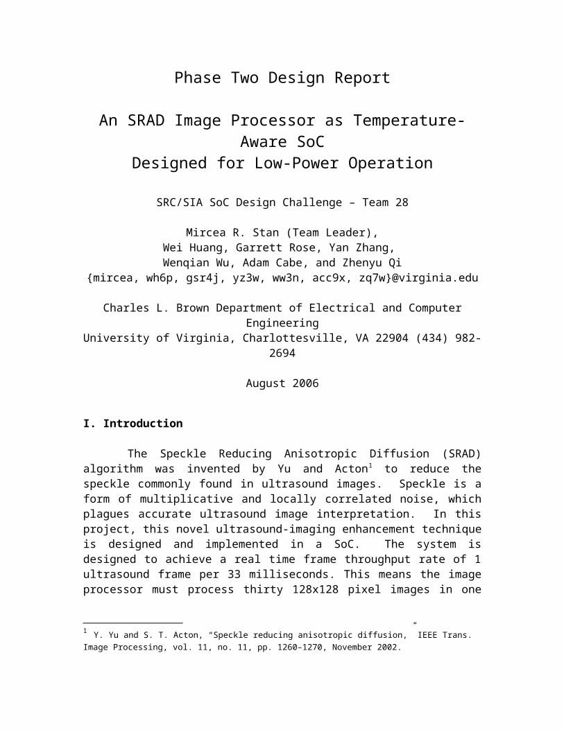
B. Design MethodologyThe front-end design methodology can be seen in Figure 3. Cadence ASIC and
custom design tools have been used for the design of this system. For custom layout of standard cell libraries, memories and thermal circuits, we use Cadence Virtuoso. For top-down design, we use Cadence RTL Compiler and Encounter. For VHDL coding and simulation, we use the Xilinx ISE toolset. In the following sections, we will go through each part of the design in greater detail.
Figure 3. front-end design methodology
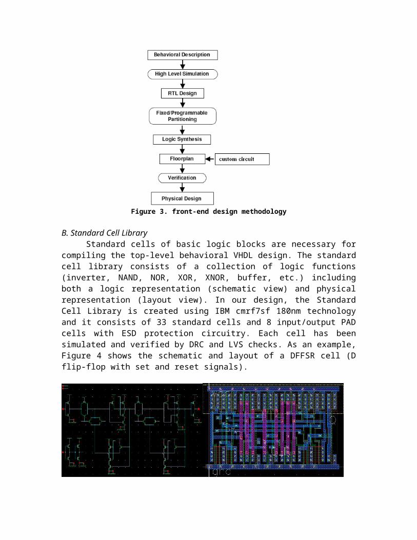
B. Standard Cell LibraryStandard cells of basic logic blocks are necessary for compiling the top-level
behavioral VHDL design. The standard cell library consists of a collection of logic functions (inverter, NAND, NOR, XOR, XNOR, buffer, etc.) including both a logic representation (schematic view) and physical representation (layout view). In our design, the Standard Cell Library is created using IBM cmrf7sf 180nm technology and it consists of 33 standard cells and 8 input/output PAD cells with ESD protection circuitry. Each cell has been simulated and verified by DRC and LVS checks. As an example, Figure 4 shows the schematic and layout of a DFFSR cell (D flip-flop with set and reset signals).

(a) schematic (b) layoutFigure 4. Schematic and layout of DFFSR cell.
C. VHDL DescriptionThe top-level description of this design is written in VHDL. Preliminary
implementation of the design has been tested using an FPGA-based system. The actual SRAD algorithm has also been verified using MATLAB.
For this SoC design, the original VHDL has been modified from that used on the FPGA prototype. We have done extensive functional simulations. Part of the VHDL simulation results are shown and described in this section. Simulations were also completed for the verilog netlist of the overall design. The verilog netlist is obtained as an output from Encounter after clock-tree buffers have been inserted. All synthesized functional sub-blocks have been verified and compared with the results of VHDL simulation. Due to the length of those simulations, we choose to include the detailed sub-block VHDL/verilog simulations in the final report.
1. Global control unit Figure 5 shows the simulation results from the global control unit. When the signal
“NewFrm” goes to ‘1’ a new frame has been loaded into the input buffer and is waiting to be processed. The state of the control unit then switches from “Idle” to “RdInBff”.
Figure 5. Simulation results of global control unit.
2. Video input controller The following simulation verified that the input controller is able to generate the
correct addresses for the input buffer RAM.
Figure 6. Simulation results of video input controller.
3. VGA output control Generation of the output buffer address and VGA synchronization signals has been
verified by simulation as shown below.
Figure 7. Simulation results of VGA output controller.
4. Mode selectionFor different input modes, the mode selection module sent different control points
to all the multiplexers in the design.
Figure 8. Simulation results of mode selector.

Figure 9 shows the entire top-level VHDL design in schematic form.
Figure 9. Top level design
D. RTL CompilationOnce we have the whole system described in a hardware description language, in
our case VHDL, Cadence RTL Compiler is then used to synthesize the system into a gate level netlist based on the standard cell library. This netlist has all of the connection information among those instantiated standard cells and is ready to be used by the place and route tool (Encounter). RTL Complier has proven to be very suitable for our SRAD design since it includes many datapath-targeted optimization techniques, such as the carry-save optimization for the extensively used multipliers in our design.
The custom designed parts, including the memory (RAM/ROM) and temperature sensors are treated as black boxes in this synthesis step. RTL complier won’t interfere with the interconnection within black boxes but still provides the interface to the other parts.
The IO pads also need to be taken care of at this step so that they can be readily incorporated into the place and route tool. Basically, we took all the other parts including the synthesized standard cells and custom designed parts mentioned above as one big module and connected all of the pins with the IO pads, forming the top-level module. With everything included in the netlist, the design was then ready for placement and routing.
E. Memory DesignAs stated previously, the top-down methodology is suitable for a majority of this
chip (e.g. IO control unit, SRAD, etc.). In general, with the appropriate tools in place, synthesis from VHDL down to a place-and-route layout is a more efficient way to layout

a digital circuit. However, our memory does not fit this generality. Memory needs to be as compact and fast as possible, which elicits itself to custom design.
There are five different memory blocks on chip, most of which have different characteristics. The main three memory blocks are SRAM, consisting of standard 6T SRAM memory cells laid out for compactness and speed. One RAM is a 32-kilobyte, 16 bit output memory used in conjunction with the SRAD image processor core. The other two RAMs are 16-kilobyte, 8 bit output memories used for image input and output. Each RAM is broken apart into individual 8-kilobyte, 4 bit output blocks (as can been seen in Figure 10 and Figure 11), allowing each overall RAM to be created using several of these smaller RAM blocks. These smaller blocks could in a sense be viewed as “banks”. This is why there appear to be 8 individual blocks of RAM on the chip layout in Figure10. Four of these blocks make up the SRAD processor memory, and the other four make up the input and output buffer RAM. The last two memory blocks are ROM units used in the on chip control units. Both ROMs are implemented using standard NOR-plane type ROMs, and contain the code sequences to enable both the input video controller and test mode selection.
The final 6T SRAM cell size is 3.5x4 um, which leads to 16-kilobyte memory size of approximately 1.79x1.03 mm. We wrote our own memory generator to construct the layout of the RAM and ROM from single memory cells. Total area coverage of the 64-kilobytes of on die memory is 3.58x2.06 mm. This is about 30% of the total allotted 5x5mm die size, and about 42% of the actual final die size (4.96x3.6 mm). Since the ROM units contain very few lines of instruction (10 or less), the layouts are compact and fairly negligible in terms of area of the overall chip.
III. Layout
A. LIB file and LEF fileThe LIB file is used to characterize the timing response and power consumption
for the standard cells and custom-designed modules, and is required for both RTL Compiler and Encounter. In our design flow, we use Cadence SignalStorm to generate the LIB file. SignalStorm reads the extracted transistor netlist in SPICE format, then automatically generates a library characterization database and performs transistor-level circuit simulations on all possible logical combinations of input and output signals. The output cell characterization data in the LIB file include logic, delay, power, and gate capacitance information. The LIB file will be used in RTL Compiler to create a gate-level netlist. It is also used by Encounter for delay calculation, timing analysis and clock tree synthesis.
The LEF file is needed by Encounter for physical metal shapes of the standard cell library and the custom designed circuits of our design (e.g. SRAM array, ROM, thermal sensors, IO pads). The LEF file is generated by Cadence Abstract Generator. The first part of this file describes technology related information such as metal/via width and pitch. It also includes via generation rules to be used by routing interconnects in Encounter. In the LEF file for our standard library, we adopt the lambda rules enforced by OSU standard cell library. For the SRAM and ROM array, we generated power rings

for these modules. All routing and blockage information for each cell and custom designed modules are provided in the LEF file.
Another technology related file is the wire resistance and capacitance table for the IBM cmrf7sf technology. We manually specify the metal/dielectric layer information by referring the IBM cmrf7sf design manual. Then we use generate_captable in Cadence Encounter to generate the extracted RC information for all metal layers. This file is used by Encounter to calculate wiring delay while routing interconnects, during timing analysis and for timing optimization.
B. EncounterFor place and route, we use Cadence First Encounter, which is simply referred to
as Encounter. This is a quite powerful tool and is a key step in our design. Basically, Encounter takes in the logic-level netlist generated from RTL Compiler, plans the power/ground grids, places all of the standard cells as well as black-boxes, synthesizes clock trees based on given timing constraints, routes all wires and adds metal fills to satisfy the pattern density check required for fabrication. In this process several issues need to be taken care of.
First, to correctly place the standard cells (i.e., connect them with metal wires and put vias at appropriate places without violating the design rules) an LEF file associated with the specified technology is needed. This file not only has all the standard cell information and via information, but also has a set of DRC rules for Encounter to observe and check with its own placement and routing.
Second, a LIB file and a timing constraint file are needed for the purpose of clock tree synthesis. The LIB file provides information about the clock(s) including timing constraints, input/output delay, clock transition time, latency and clock skew, etc. Encounter is able to generate multiple clock trees, possibly related to each other, with different timing constraints and load information.
Figure 10 shows an overview of the chip after placement and routing.
Figure 10. Chip layout in Encounter

C. Memory LayoutSince there are five different memories on chip, it is impractical to build each
individual memory block by hand. We have designed our own memory generator in order to efficiently create each individual memory block. This memory generator is capable of taking the most basic memory blocks, and creating a memory based on certain size parameters (i.e. number of bits per word, number of rows, number of columns, etc). The generator was used to construct everything in the memory, including the VDD and ground rings for power distribution throughout the SRAM. This generator was implemented entirely in the Cadence SKILL language. Below is a layout of the generated, 8-kilobyte, 4 bit output SRAM block.
Figure 11. Layout of 8KB memory block.
Simulating the memory proved to be an arduous task due to the immense size of the memory blocks. The first simulations performed were only on small memories. Here the functionality of the memory was observed to show that the memory operated as planned. DRC and LVS were run to show that the generator functioned properly, and functional tests were performed both on the memory schematic and layout extraction. Next a model was constructed to emulate the operation of an 8-kilobyte memory. The schematic of this model consisted of four standard memory cells to represent each corner of the memory, a number of dummy memory cells to emulate the leakage seen over the entire column being read, some RC delay blocks to emulate the resistance and capacitance of the wires connecting the memory cells, and the standard address decoders to read and write the memory. Simulations were run on this compact model to determine

whether or not the large memory banks would work. This model also helped determine certain sizing and logical drive parameters within the memory. The simulation of the model below proved that the memory did indeed work, showing a worst-case “slow-slow” corner delay of just under 1 ns for a read, and slightly less than that for a write. In this simulation, the plot on the very top is the R/W enable signal, the strip just below the top is the memory clock, and the strip at the very bottom is the memory output. When the R/W enable signal is low, the memory is enabled to write, and when that signal is high, the memory is enabled to read. In the first write cycle, a ‘1’ is written into one bit of memory, and then it is read out on the following read cycle. On the second write cycle, a ‘0’ is written into one bit of memory, and then it is read out on the following read cycle.
Figure 12. Simulation results of memory block.The model verification assured that the large 8-kilobyte memory block would work. Lastly, DRC was performed on the overall memory layout, verifying that the memory was complete.
IV. Power and Thermal ConsiderationsWe have also implemented 8 temperature sensors in the design. Each of them is a
7-stage ring oscillator, with output frequency ranging from ~700MHz to ~1GHz for different operating temperatures. Each sensor’s frequency is divided by 16 and one of the

sensors’ outputs is selectively connected to an output pad for off-chip observation. The size of each sensor is 14.4um x 10um. We use 6 of the 8 sensors to measure the temperatures of Input Buffer, SRAD memories and Output buffer. These sensors are located between SRAM memory blocks. Two other sensors are located in the middle stripe of the die where SRAD unit resides. Since the SRAD unit is computationally intensive, it is necessary to be able to observe the temperature of its different locations. The simulated output sensor frequencies for different temperature levels are shown in the following chart.
40
45
50
55
60
65
0 25 50 75 100
Temperature (C)
outp
ut fr
eque
ncy
afte
r div
ided
by
16
Series1
Figure 13. Temperature sensor’s response to operating temperature.
When the fabricated chip comes back, the temperature sensors are going to be calibrated first in an oven set to different temperature levels. During run-time, the sensors’ output can be used to implement off-chip dynamical thermal management such as Dynamic Voltage Scaling (DVS). We also put a custom circuitry on the die which includes FO4-loaded ring oscillators for temperature sensing. The circuit can also dynamically reduce the leakage power by adjusting n-well body bias voltage according different levels of operating temperature.
V. Testing
A. Testing Generics- FPGA prototype of SRAD, shown in Phase I report.- How will we test – test bench, FPGA, logic analyzer- Off-chip clocking, need a 200 MHz crystal
B. Modes of Operation for Ad-hoc Testing A significant portion of this work is focused on designing for test, enabling us to
thoroughly examine the detailed functionality of the final chip. Basically, this is done ad-hoc by using existing on-chip resources. As a designer, one has to always design for the worst-case scenario, and this truism is imperative when designing for testability. Although each block on this chip interacts with one another in real time, the system as a

whole is capable of being broken down into separate blocks for testing. A series of multiplexers, decoders, and control inputs are present throughout the chip, which allows the tester to isolate individual blocks throughout the system. There are three control logic input pins into the system, which allow for eight modes of operation. Here is a complete list of the modes of operation:
1. I/O Interface Test : Two very basic tests will be performed to ensure the proper operation of the I/O circuitry. One test connects one pad to the input of an inverter, and another pad to the inverter output to verify that a simple inverter works, and to verify that the pads input and output in the correct manner. The second test will simply involve outputting the on chip clock to verify that the pad does not affect the clock in a malicious manner.
2. Input Buffer Test : During this mode, we are able to test the functionality of the input SRAM unit. In order to test the total functionality of this block, and ensure isolation from the rest of the chip, all of the SRAM inputs will come from off die. To conserve pins, the data input into the RAM will also be used as part of the memory address. The rest of the memory address will come from pins that are not used during the memory only mode.
3. Output Buffer Test : During this mode, we are able to test the functionality of the output SRAM unit. Like the input SRAM test, all of the inputs will come from off die. To conserve pins, the data input into the RAM will again be used as part of the memory address. The rest of the memory address will come from pins that are not used during the memory only mode.
4. SRAD Unit Test : This mode will solely be used to verify the functionality of the SRAD image processing core. The input to this block will come from off chip, and since the SRAD is a deeply pipelined block, the input and output will travel over the same data bus and use the same pins. This test mode will isolate the SRAD unit from the rest of the on chip memory, and will verify that the input pixels are indeed processed in the correct way.
5. SRAD Loop Test : This test mode will isolate the main SRAD processing loop from the rest of the chip. The tested blocks will be the main SRAD memory, the window generator (shift register), and the SRAD unit. This test will verify that these individual blocks work together as expected.
6. Preprocessing Block Test : This test is designed to test the preprocessing exponential unit. This block is designed to convert the input 8-bit data byte into a 16-bit word for use in the SRAD processing block.
7. Shift Register Test : During this mode, the user is able to isolate the shift register used in the SRAD processing loop to verify its functionality. System clock skew can often lead to errors in shift registers. This test is designed to make sure that the clock skew does not lead to a failed shift register.
8. Entire System Test : The last test will be to simply verify the functionality of the entire system put together. Here we will check three versions of our system. The first will require only one image processing iteration, basically to see that the picture we put in is the picture we get out. The second will require 50 processing iterations, which will require a slower clock frequency than the full image processing technique, and should simply allow us to make sure that every piece of

the system works together as it should. The last will be to run the full 100 iterations in the image processor with plans to achieve the fully processed real time image output.
C. The Printed-Circuit Board
Before the fabrication of our design was finished (10 packaged, 30 unpackaged), we designed a printed-circuit board (PCB) to test the packaged chips. The PCB is shown in Figure 14. More details about the PCB are listed below:
Figure 14. The testing PCB.
a. There is a LCC44 testing socket.b. There are four logic analyzer connectors to apply stimuli to the chip and
observe outputs from the chip using logic analyzer. c. There are also three 60-pin connectors to connect our testing board to an
FPGA prototype board. By doing this, we can individually test some modules of the design and bypass the other modules by replacing them with FPGA board. The FPGA board can be flexibly configured to implement part or all of the functional modules of the design.
d. A 9V power supply is supplied off-board, and is regulated to generate local 1.8V and 3.3V supplies for the chip. 3.3V for IO, and 1.8V core voltage.
e. A number of test points are deployed across the board to observe the quality of critical signals such as clock input, clock output, power supplies, etc.
f. We have design the test board so that the 100MHz clock can be applied from several sources: an on-board clock oscillator, the FPGA prototype board, an off-board frequency generator, or a logic analyzer.
g. To ensure stable power supply and clock signal to the chip, we have added a number of decoupling capacitors, for example, near the chip package, the voltage regulators, and the clock oscillator.

h. The global reset signal for the chip is generated by a MAXIM de-bouncer, and is initiated by a push button on the board. Thus, we can have asynchronous global reset signal with reasonable pulse duration.
D. Testing Results
As a starting point, we first tested the custom-designed pad frames (Item No.1 in Section V-B). On the die, we put a simple test structure connecting an input pad to an output pad via a wide inverter—INVX8, which is the widest one available in the standard cell library. The core voltage supply is 1.8V, and the IO voltage supply is 3.3V.
In the output pad, there is an output driver designed to drive the large off-die capacitive load with guard rings to prevent latch-up. There is also a level converter to make the output signal swing from 0 to 3.3 volt. In the input pad, there is ESD protection circuitry and an input level converter to shift the input signal swing from 3.3V to 1.8V. The input level converter is connected to a wide inverter acting as input signal buffer. The output of this input signal buffer is then fed into the core logic or memory blocks.
During the first test, we found that when applying different input voltage levels to the above-mentioned test structure, the corresponding output pad is always floating. We then checked the board power supplies by probing the on-board test points. We also probed the power and input signal pins on the LCC44 sockets, all of which were at the correct levels. We then isolated and probed the LCC44 package itself to make sure that all the 1.8V pads, 3.3V pads, GND pads are shorted within the package, respectively. At this point, we found that significant resistance exists among most of the power supply pads. For example, there is 100K resistance between two 1.8V supply pads. By inspecting the final layout of the design, we did not find any obvious errors in the layout connection of power supply rails and pads. We then suspected there might be something wrong with the wire-bonding. By inspecting the wire-bonding under a microscope, and we found that the die was rotated 180 degrees during the wire-bonding process compared to the desired wire-bonding diagram that we provided. This is due to the misunderstanding of the wire-bond diagram format and lack of communication between our team and the packaging staff. The result is that most of the 44 pads out of the entire 60 pads were connected to the wrong pins on the package. Some of the pads were not even wire-bonded to a package pin.
Somewhat luckily, we designed the GND pins symmetrically on the pin-out, so all the GND pins are connected correctly even with the presence of the wire-bonding error. In addition, all the pads needed to test the input-pad-inverter-output-pad were also available on the package. So we re-applied the power supplies and input signals to the corresponding new set of pins on the package. This time, the output pad connected to the output of the inverter still did not follow the inversion of the input signal. So we double-checked the extracted simulations of the input pads, the inverter and the output pads, sweeping both the input and supply voltages. All simulations worked as expected for all the voltages and capacitive loads. Then we inspected the final layout, starting from the input pad. Here we found a fatal error in the input pad—there is a gap (absence of metal) between the output of the level converter and the input signal buffer, as shown in Figure15. While the extracted view simulation worked, the original layout view was modified most likely during the modification of either the level-converter cell or the input signal

buffer cell, which resulted in creating a tiny gap that just passed DRC. Unfortunately, the extracted view was not automatically updated after this minor modification to catch this mistake. This simple but fatal mistake rendered every single input pad unusable; thus the whole design not testable. This is a huge lesson of custom design that we have learned in the hardest way. In the next section, we list all the lessons that we have learned from this valuable SOC design experience.
Figure 15. The gap in M1 that was not updated in extracted view.
F. Lessons Learned
1. To avoid slow, tricky and error-prone full-custom design, always first try to find available libraries or components. In our case, we should put every effort to find an available pad frames for the IBM 0.18um BiCMOS process. The existence of such IO pad frame would have significantly reduced our design effort and would have prevented the fatal mistake that we made during the custom layout of the input pad.
2. Extreme care should be taken when designing custom circuits. There should be a script to automatically update each and every view of the custom-designed circuit, as long as there is a change in one of the views. Also, extracted view generation, DRC and LVS should also be automated for every modification of the design. In addition, extensive simulations at all corners are required to make sure the circuit works. Ideally, this should be version controlled, such that the circuit and the design can be recovered from an older version in case the new version has something wrong. The rule of thumb, never trust manual design—check, double check and triple check!
3. Avoid making any non-necessary changes after a designated point in the design schedule. It is very easy to make mistakes, and even harder to catch mistakes when design decisions are still being implemented late in the design effort. If these changes are necessary, always keep at least two or three pairs of eyes on the changes to make certain that no small mistakes are made.

4. When planning the pad frames and the pin out, it is helpful to make the pin-out as symmetrical as possible, so that whenever there is something with the orientation during wire-bonding, most of the critical signals are still connected in the correct way. This can get the most out of one batch of chips before issuing a re-spin.
5. Document as much as possible during the entire design flow. This includes both the design and the tools. By doing this, significant effort will be saved for future design review, testing and even for the next new design project.
VI. Summarized Design Issues
1. Version control — this includes all the hierarchies of the design: leaf cells, macros built from leaf cells, units built from macros, and the entire design. This also includes all the design views: schematic, layout, extracted views, GDS file, and supporting simulation files and scripts.
a. Whenever one cell (or view) is modified, update all the related macros/units/system. Ideally, this should be an automated process through scripting.
b. Make fully designed and simulated cells (and views) write-protected to prevent accidental modifications.
c. Ideally, every modification should be double-checked by another designer to make sure there are no surprises after the modification.
2. Abstract Generator — standard cells and custom-designed blocksa. The layout of every cell should be as symmetrical and possible, especially
for shapes such as NWELL, VDD/GND contacts. This is required because adjacent rows of standard cells share the same VDD or GND, asymmetrical power supply contacts and wells may cause DRC errors.
b. In Abstract Generator, standard cells, IO pads and custom blocks need to be treated separately. For custom blocks such as memories, because they will be treated as black-boxes in RTL Compiler and Encounter, they should be put into “Block” bin in AbGen, and generate power ring pin to assist power rail routing in Encounter.
3. RTL Compilera. In some units, errors occur during synthesis from VHDL code, with
signals directly connected to “1” or “0”.b. The manual says there is timing and power analysis capabilities in RTL
Compiler, need to clarify how to do it, and what are the difference from doing it in Encounter.
c. Still not totally clear about the timing constraint file (sdc file). For example, how to set different constraints, what constraints are required, and how to specify multiple generated clocks from the same clock source.
6. Encountera. Power grid generation and layout: how to assign more than one power
supply in Encounter? What is the correct power grid density on each metal layer?
b. What are the exact procedures to do clock synthesis and what should be in the timing constraint file?
7. SignalStorm — library characterizationa. Configuring SignalStorm to run with Spectre is tricky. Especially for cells
with feedback signals such as flip-flops and latches. SignalStorm always complains about some internal signal (assigned with a random name) doesn’t have path to GND.
b. How to characterize memory blocks? Using SignalStorm is unreasonable. One way is two build a simplified memory model to get timing and power information at different process corners. Also need to pay attention to read and write noise margins.
8. DRC and LVS for the entire designa. Overall DRC can be achieved by using Assura hierarchical DRC.b. Overall LVS can also be done with Assura hierarchical LVS, but the
process can be very slow. c. Another issue with LVS is how to generate hierarchical schematics. We
have been able to generate flat schematic of the entire design from the final Verilog netlist with scripts running IHDL. But doing LVS with this schematic and the flattened layout yield too many repetitive LVS errors that are very hard to locate and fix.
9. Tape-outa. Make sure the orientation of the die in the bonding diagram is correct. Call
or email the packaging factory if needed. Wrong orientation could yield the entire package not testable.
VII. Conclusions
In this report, the entire design flow of the SRAD processor is presented. More details regarding physical design and simulation results of key parts of the design are also shown. Testing plans and the unsuccessful test results are analyzed. Lessons learned from this design experience are also reviewed. Despite the failure of the silicon test, it has been a great exploration experience for the entire design team. From the conceptual design, to the proposal for the first phase of this contest, to the physical design during phase two, the entire team has gained a lot of experience and knowledge, together with the joy of team work from this project. Since the core part of the design has not been tested, we would consider a re-spin in the future when situation permits.