Embed Size (px)
Citation preview

Week 7
Input/Output Interface Circuits and LSI Peripheral Devices
2
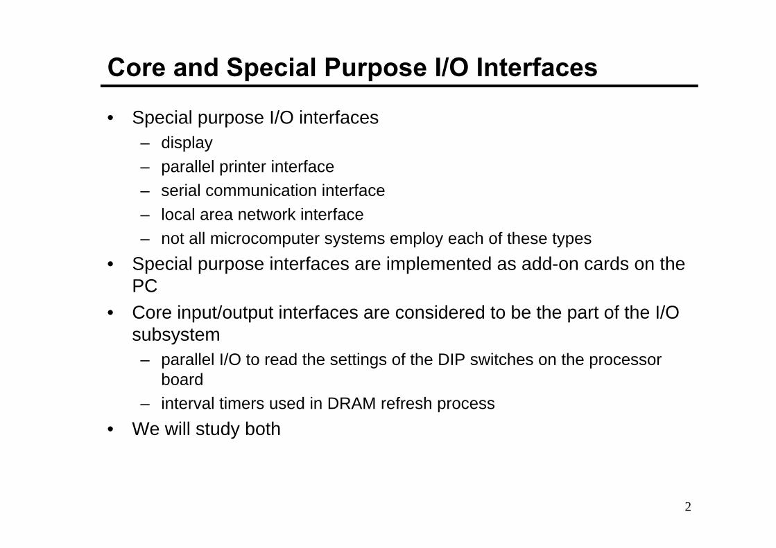
Core and Special Purpose I/O Interfaces
• Special purpose I/O interfaces– display
– parallel printer interface
– serial communication interface
– local area network interface
– not all microcomputer systems employ each of these types
• Special purpose interfaces are implemented as add-on cards on the PC
• Core input/output interfaces are considered to be the part of the I/O subsystem– parallel I/O to read the settings of the DIP switches on the processor
board
– interval timers used in DRAM refresh process
• We will study both
3
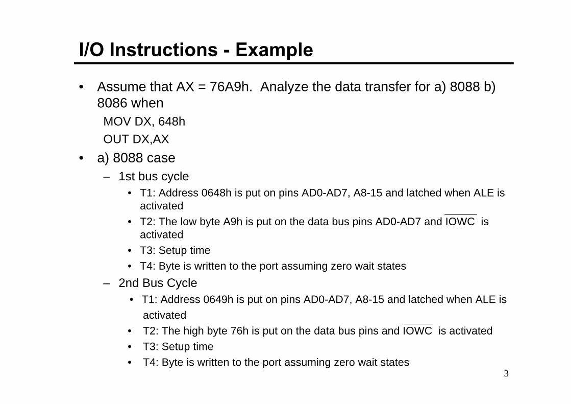
I/O Instructions - Example
• Assume that AX = 76A9h. Analyze the data transfer for a) 8088 b) 8086 whenMOV DX, 648h
OUT DX,AX
• a) 8088 case– 1st bus cycle
• T1: Address 0648h is put on pins AD0-AD7, A8-15 and latched when ALE is activated
• T2: The low byte A9h is put on the data bus pins AD0-AD7 and IOWC is activated
• T3: Setup time
• T4: Byte is written to the port assuming zero wait states
– 2nd Bus Cycle• T1: Address 0649h is put on pins AD0-AD7, A8-15 and latched when ALE is
activated
• T2: The high byte 76h is put on the data bus pins and IOWC is activated
• T3: Setup time
• T4: Byte is written to the port assuming zero wait states
4
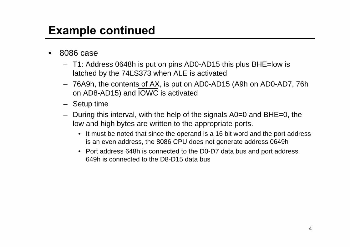
Example continued
• 8086 case– T1: Address 0648h is put on pins AD0-AD15 this plus BHE=low is
latched by the 74LS373 when ALE is activated
– 76A9h, the contents of AX, is put on AD0-AD15 (A9h on AD0-AD7, 76h on AD8-AD15) and IOWC is activated
– Setup time
– During this interval, with the help of the signals A0=0 and BHE=0, the low and high bytes are written to the appropriate ports.
• It must be noted that since the operand is a 16 bit word and the port address is an even address, the 8086 CPU does not generate address 0649h
• Port address 648h is connected to the D0-D7 data bus and port address 649h is connected to the D8-D15 data bus
5
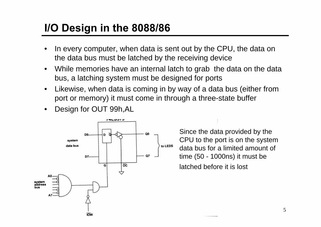
I/O Design in the 8088/86
• In every computer, when data is sent out by the CPU, the data onthe data bus must be latched by the receiving device
• While memories have an internal latch to grab the data on the data bus, a latching system must be designed for ports
• Likewise, when data is coming in by way of a data bus (either from port or memory) it must come in through a three-state buffer
• Design for OUT 99h,AL
Since the data provided by the CPU to the port is on the system data bus for a limited amount of time (50 - 1000ns) it must be
latched before it is lost
6
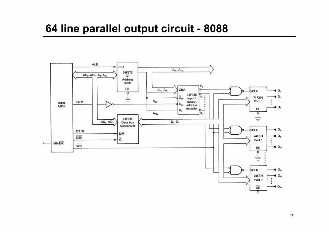
64 line parallel output circuit - 8088
7
Examples
• To which output port in the previous figure are data written when the address put on the bus during an output bus cycle is 8002h– A15 .. A0 = 1000 0000 0000 0010b
– A15L = 1
– A0L = 0
– A3L A2L A1L = 001
– P1 = 0
• Write a sequence of instructions that output the byte contents of the memory address to output port 0 in the previous figure
8
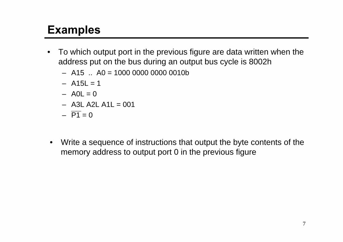
Time Delay Loop and Blinking a LED at an Output
MOV DX, 8000h ;initialize address of port 0MOV AL, 00h ; load data with bit seven 7 as logic 0
ON_OFF: OUT DX,AL ; turned onMOV CX,0FFFFh ; load delay count of FFFFh
HERE: LOOP HERE XOR AL,80h ; complement bit 7JMP ON_OFF
9
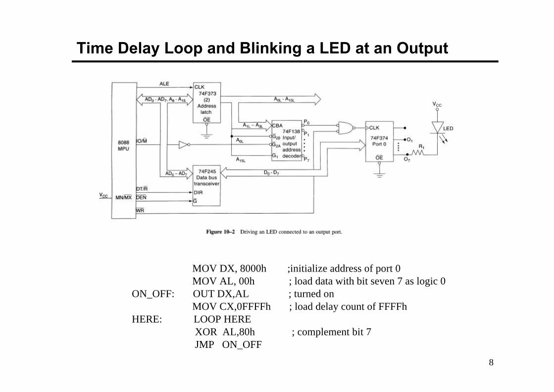
IN port design using the 74LS244
• In order to prevent any unwanted data (garbage) to come into the system (global) data bus, all input devices must be isolated through the tri-state buffer. The 74LS244 not only plays this role but also provides the incoming signals sufficient strength (driving capability) to travel all the way to the CPU• It must be emphasized that every device (memory, peripheral) connected to the global data bus must have a latch or a tri-state buffer. In some devices such as memory, they are internal but must be present.

10
64 line parallel input circuit
Read from input port 7 to the memory location DATAMOV DX, 800EhIN AL,DXMOV DATA, AL
11
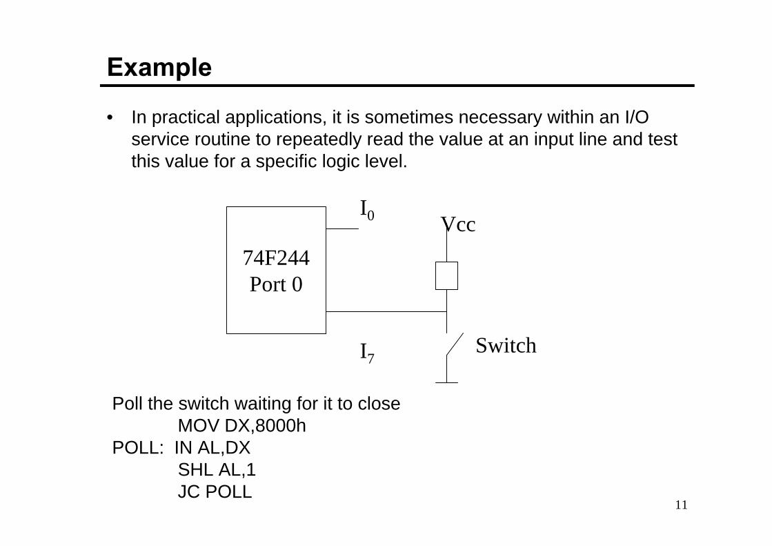
Example
• In practical applications, it is sometimes necessary within an I/O service routine to repeatedly read the value at an input line and test this value for a specific logic level.
74F244Port 0
I7
I0 Vcc
Switch
Poll the switch waiting for it to closeMOV DX,8000h
POLL: IN AL,DXSHL AL,1JC POLL
12
Input Output Handshaking
• The I/O ports of a computer typically operate at different data rates
• A hard disk drive, for example, might require the computer to input data at 10Mbps
• CD-ROM drives operate at 300-600 Kbps
• However when inputting keystrokes from the operator, the data rate may fall to only one or two characters per sec.
• If the processor is to operate efficiently, one needs to develop a strategy to control or synchronize the flow of data between the processor and the widely varying rates of its I/O devices
• This type of synchronization is achieved by implementing what is known as handshaking as part of the input/output interface
• Printers typically have buffers that can be filled by the computer at high speed
• Once full the computer must wait while the data in the buffer isprinted
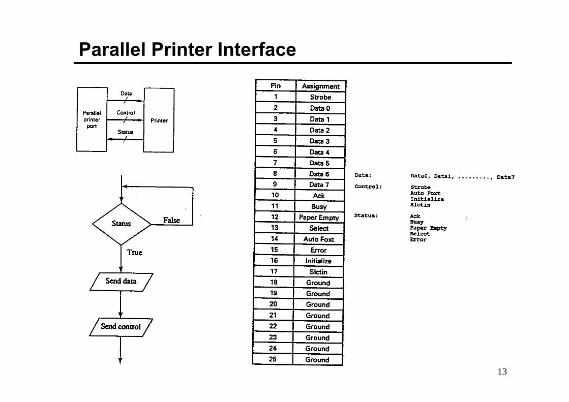
• Most printer manufacturers have settled on a standard set of data and control signals Centronics Parallel Printer Interface
13
Parallel Printer Interface
14
Handshaking
15
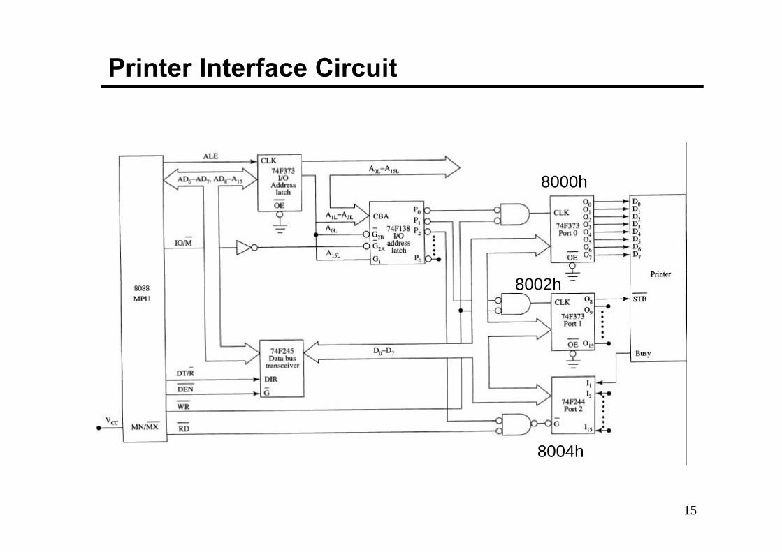
Printer Interface Circuit
8000h
8004h
8002h
16
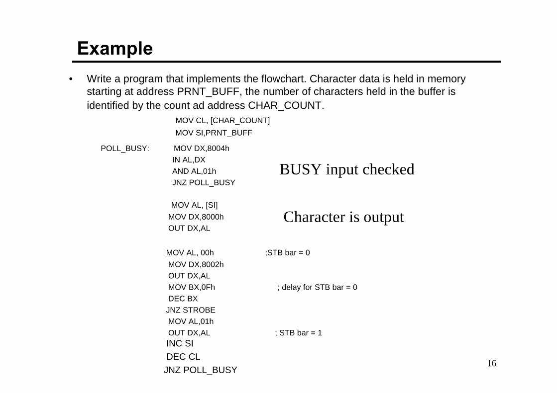
Example
• Write a program that implements the flowchart. Character data is held in memory starting at address PRNT_BUFF, the number of characters held in the buffer is identified by the count ad address CHAR_COUNT.
MOV CL, [CHAR_COUNT]
MOV SI,PRNT_BUFF
POLL_BUSY: MOV DX,8004h
IN AL,DX
AND AL,01h
JNZ POLL_BUSYBUSY input checked
MOV AL, [SI]
MOV DX,8000h
OUT DX,ALCharacter is output
MOV AL, 00h ;STB bar = 0
MOV DX,8002h
OUT DX,AL
MOV BX,0Fh ; delay for STB bar = 0
DEC BX
JNZ STROBE
MOV AL,01h
OUT DX,AL ; STB bar = 1INC SI
DEC CL
JNZ POLL_BUSY
17
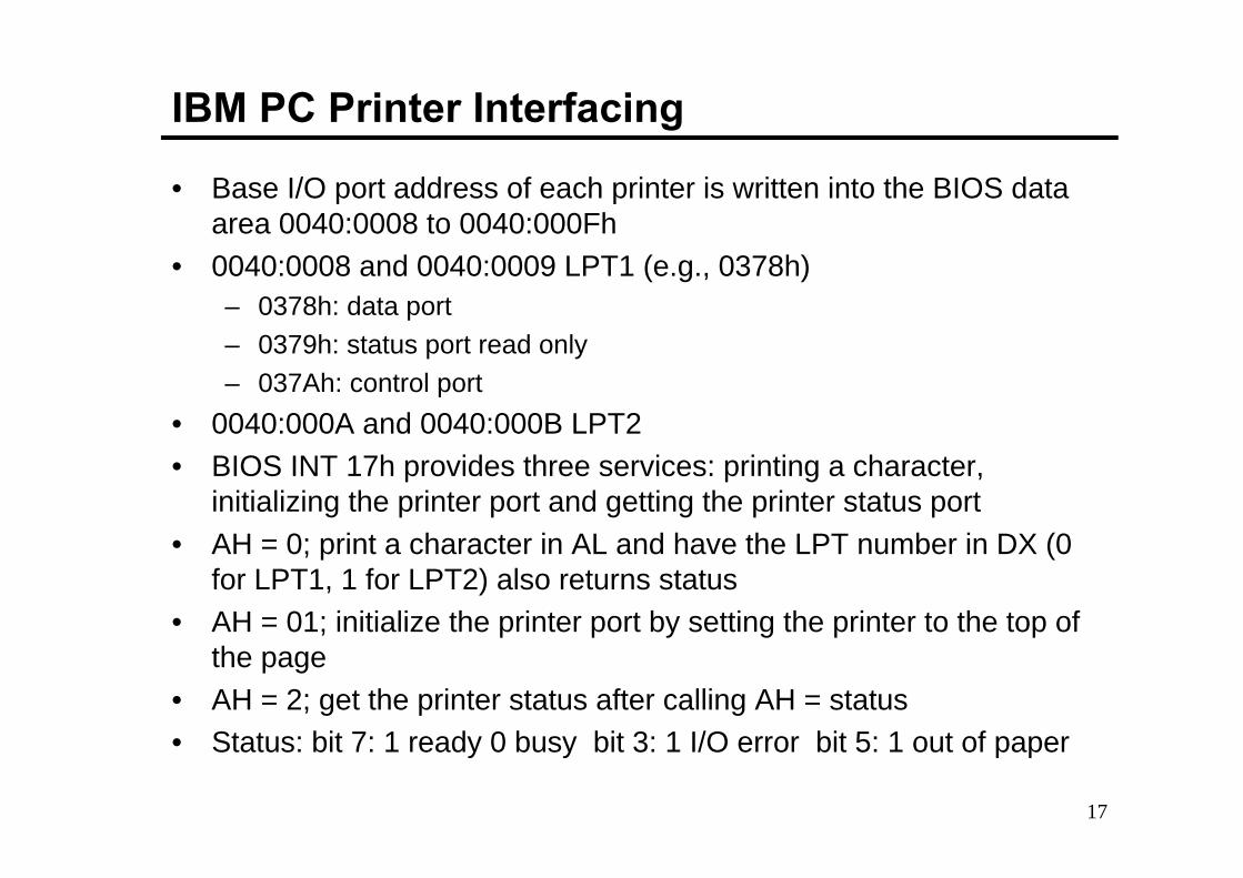
IBM PC Printer Interfacing
• Base I/O port address of each printer is written into the BIOS data area 0040:0008 to 0040:000Fh
• 0040:0008 and 0040:0009 LPT1 (e.g., 0378h)– 0378h: data port
– 0379h: status port read only
– 037Ah: control port
• 0040:000A and 0040:000B LPT2
• BIOS INT 17h provides three services: printing a character, initializing the printer port and getting the printer status port
• AH = 0; print a character in AL and have the LPT number in DX (0for LPT1, 1 for LPT2) also returns status
• AH = 01; initialize the printer port by setting the printer to the top of the page
• AH = 2; get the printer status after calling AH = status
• Status: bit 7: 1 ready 0 busy bit 3: 1 I/O error bit 5: 1 out of paper
18
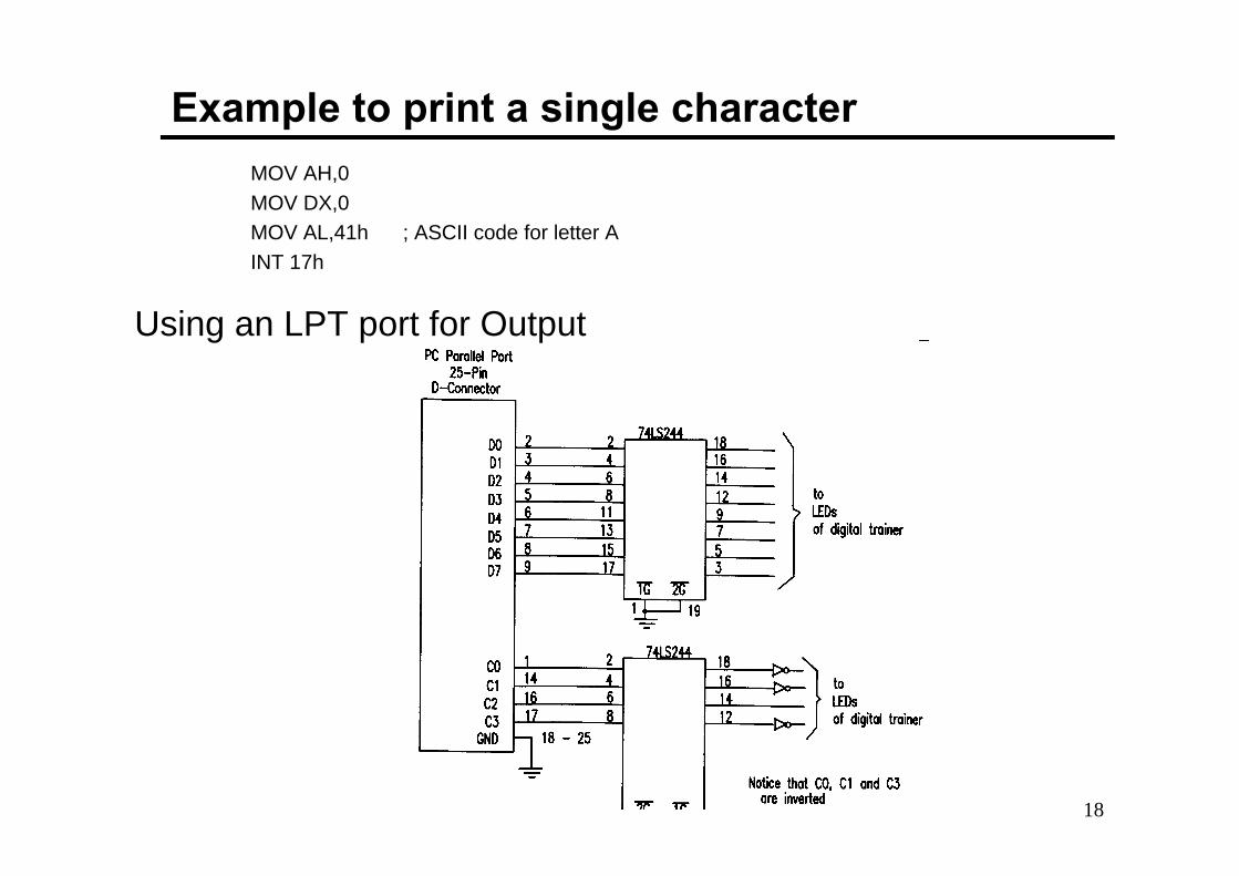
Example to print a single character
MOV AH,0
MOV DX,0
MOV AL,41h ; ASCII code for letter A
INT 17h
Using an LPT port for Output
19
The 8255 Programmable Peripheral Interface
• Intel has developed several peripheral controller chips designed to support the 80x86 processor family. The intent is to provide a complete I/O interface in one chip.
• 8255 PPI provides three 8 bit input ports in one 40 pin package making it more economical than 74LS373 and 74LS244
• The chip interfaces directly to the data bus of the processor, allowing its functions to be programmed; that is in one application a port may appear as an output, but in another, by reprogramming it as an input. This is in contrast with the 74LS373 and 74LS244 which are hard wired and fixed
• Other peripheral controller chips include the 8259 Programmable Interrupt Controller (PIC), the 8253/54 Programmable Interval Timer (PIT) and the 8237 DMA controller
20
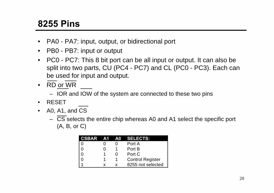
8255 Pins
• PA0 - PA7: input, output, or bidirectional port
• PB0 - PB7: input or output
• PC0 - PC7: This 8 bit port can be all input or output. It can also besplit into two parts, CU (PC4 - PC7) and CL (PC0 - PC3). Each can be used for input and output.
• RD or WR – IOR and IOW of the system are connected to these two pins
• RESET
• A0, A1, and CS
– CS selects the entire chip whereas A0 and A1 select the specific port (A, B, or C)
CSBAR A1 A0 SELECTS:0 0 0 Port A0 0 1 Port B0 1 0 Port C0 1 1 Control Register1 x x 8255 not selected
21
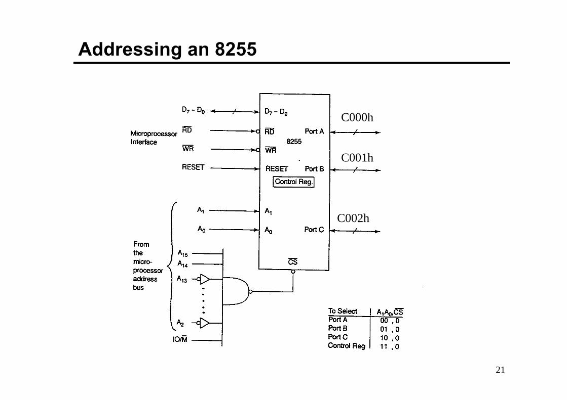
Addressing an 8255
C000h
C001h
C002h
22
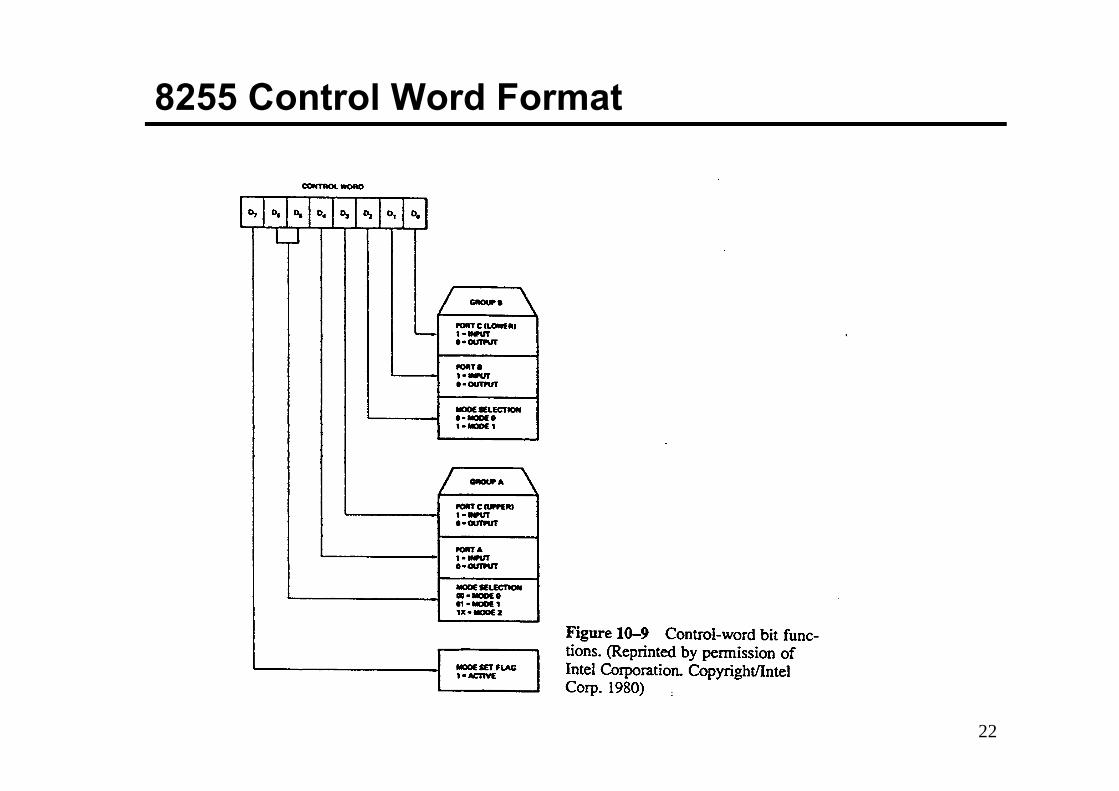
8255 Control Word Format
23
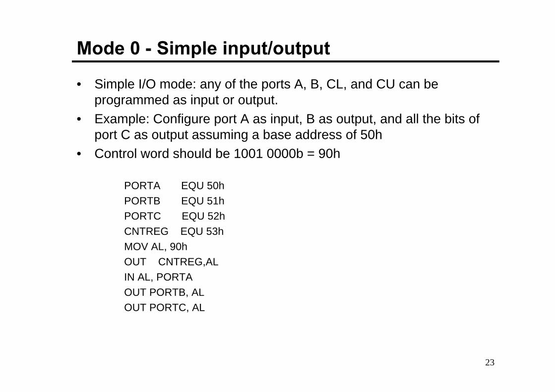
Mode 0 - Simple input/output
• Simple I/O mode: any of the ports A, B, CL, and CU can be programmed as input or output.
• Example: Configure port A as input, B as output, and all the bits of port C as output assuming a base address of 50h
• Control word should be 1001 0000b = 90h
PORTA EQU 50h
PORTB EQU 51h
PORTC EQU 52h
CNTREG EQU 53h
MOV AL, 90h
OUT CNTREG,AL
IN AL, PORTA
OUT PORTB, AL
OUT PORTC, AL

24
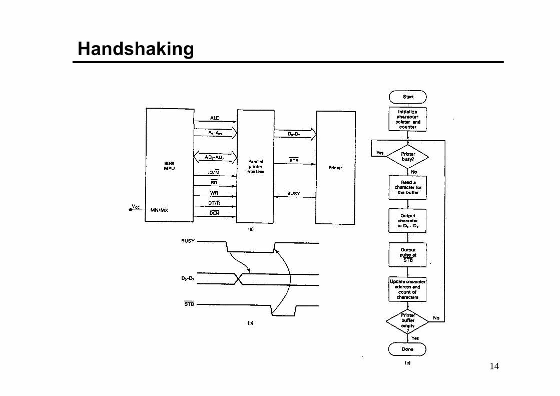
Mode 1: I/O with Handshaking Capability
• Handshaking refers to the process of communicating back and forth between two intelligent devices
• Example. Process of communicating with a printer– a byte of data is presented to the data bus of the printer
– the printer is informed of the presence of a byte of data to be printed by activating its strobe signal
– whenever the printer receives the data it informs the sender by activating an output signal called ACK
– the ACK signal initiates the process of providing another byte of data to the printer
• 8255 in mode 1 is equipped with resources to handle handshaking signals
25
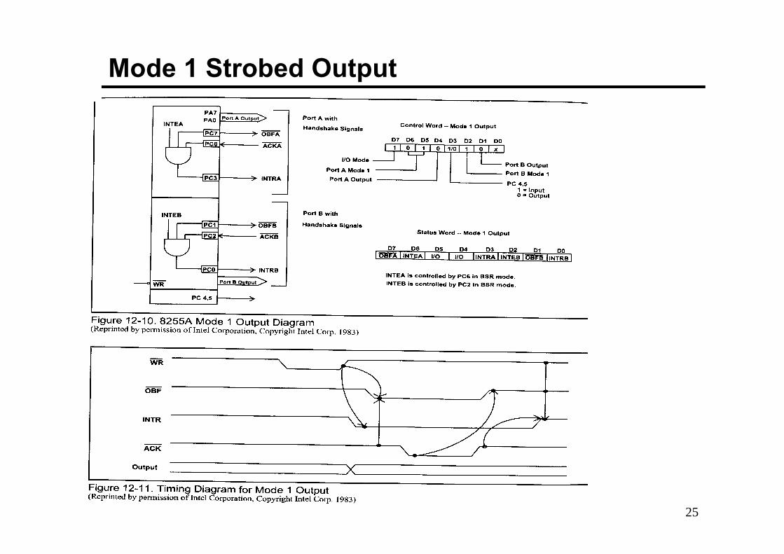
Mode 1 Strobed Output
26
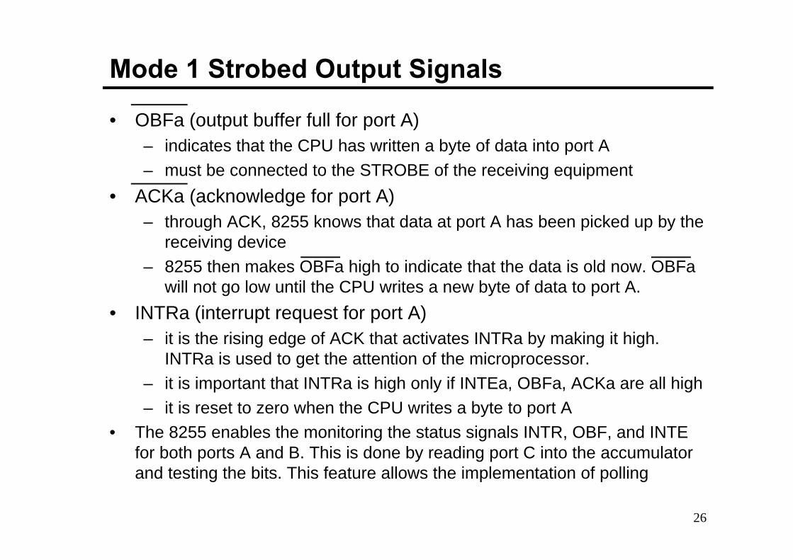
Mode 1 Strobed Output Signals
• OBFa (output buffer full for port A)– indicates that the CPU has written a byte of data into port A
– must be connected to the STROBE of the receiving equipment
• ACKa (acknowledge for port A) – through ACK, 8255 knows that data at port A has been picked up by the
receiving device
– 8255 then makes OBFa high to indicate that the data is old now. OBFa will not go low until the CPU writes a new byte of data to port A.
• INTRa (interrupt request for port A)– it is the rising edge of ACK that activates INTRa by making it high.
INTRa is used to get the attention of the microprocessor.
– it is important that INTRa is high only if INTEa, OBFa, ACKa are all high
– it is reset to zero when the CPU writes a byte to port A
• The 8255 enables the monitoring the status signals INTR, OBF, and INTE for both ports A and B. This is done by reading port C into the accumulator and testing the bits. This feature allows the implementation of polling
27
Interrupts vs Polling
• CPU services various devices in two ways:– interrupts and polling
• In the interrupt method, whenever the device needs the service of the CPU, the device informs the CPU by sending an interrupt signal.
• The CPU interrupts whatever it is doing and serves the request
• In polling, CPU monitors continuously a status condition and when the conditions are met, it will perform the service.
• The advantage of interrupts is that the CPU can serve many devices
• Each receives a service based on its priority
• Disadvantage of interrupts is that they require more hardware and software
• In contrast, polling is cheap and requires minimal software bit it ties down the CPU

28
Example
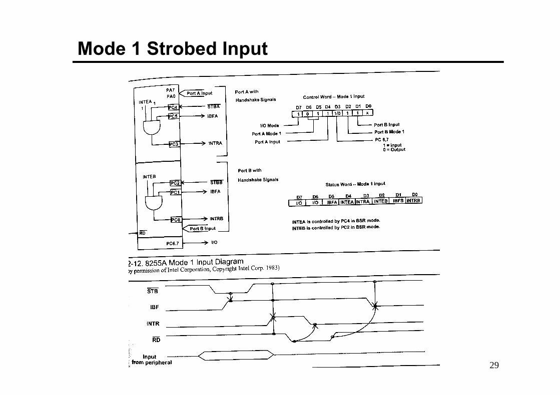
29
Mode 1 Strobed Input
30
Mode 1 Input Ports with Handshaking Signals
• STB– When an external peripheral device provides a byte of data to an input
port, it informs the 8255 through the STB pin. STB is of limited duration
• IBF (Input Buffer Full)– In response to STB, the 8255 latches into its internal register the data
present at PA0-PA7 or PB0-PB7.
– Through IBF it indicates that it has latched the data but it has not been read by the CPU yet
– To get the attention of the CPU, it IBF activates INTR
• INTR– Falling edge of RD makes INTR low
– The RD signal from the CPU is of limited duration and when it goes high the 8255 in turn makes IBF inactive by setting it low
– IBF in this way lets the peripheral know that the byte of data was latched by the 8255 and read into the CPU as well.