Embed Size (px)
Citation preview
Wavelength division multiplexed light sourcemonolithically integrated on a siliconphotonics platformPURNAWIRMAN,1 NANXI LI,1,2,* E. SALIH MAGDEN,1 GURPREET SINGH,1 MICHELE MORESCO,1
THOMAS N. ADAM,3 GERARD LEAKE,3 DOUGLAS COOLBAUGH,3 JONATHAN D. B. BRADLEY,1,4 AND
MICHAEL R. WATTS1
1Photonic Microsystems Group, Research Laboratory of Electronics, Massachusetts Institute of Technology, 77 Massachusetts Avenue,Cambridge, Massachusetts 02139, USA2John A. Paulson School of Engineering and Applied Sciences, Harvard University, 29 Oxford Street, Cambridge, Massachusetts 02138, USA3College of Nanoscale Science and Engineering, University at Albany, State University of New York, 257 Fuller Road, Albany, New York 12203, USA4Currently at Department of Engineering Physics, McMaster University, 1280 Main Street West, Hamilton, Ontario L8S 4L7, Canada*Corresponding author: [email protected]
Received 23 February 2017; accepted 31 March 2017; posted 7 April 2017 (Doc. ID 287189); published 25 April 2017
We demonstrate monolithic integration of a wavelength di-vision multiplexed light source for silicon photonics by acascade of erbium-doped aluminum oxide (Al2O3:Er3�)distributed feedback (DFB) lasers. Four DFB lasers withuniformly spaced emission wavelengths are cascaded in aseries to simultaneously operate with no additional tuningrequired. A total output power of −10.9 dBm is obtainedfrom the four DFBs with an average side mode suppressionratio of 38.1� 2.5 dB. We characterize the temperature-dependent wavelength shift of the cascaded DFBs andobserve a uniform dλ∕dT of 0.02 nm/°C across all fourlasers. © 2017 Optical Society of America
OCIS codes: (130.0130) Integrated optics; (130.3120) Integrated
optics devices; (140.3460) Lasers.
https://doi.org/10.1364/OL.42.001772
Awavelength division multiplexed (WDM) light source is a keycomponent in silicon photonics technology for application inoptical communications [1–3]. It generally consists of severaluniformly spaced optical wavelengths that can be used to en-code multiple communication channels in a common output.Several research groups have demonstrated integrated WDMlight sources of up to 16 channels by bonding of III-V gainmaterial onto the silicon chip [4–8]. However, these hybrid de-vices often require careful temperature control and complexfabrication steps with yield challenges. Alternatively, rare-earth-doped glass lasers on silicon, such as erbium-doped alu-minum oxide (Al2O3:Er
3�) or thulium-doped aluminum oxide(Al2O3:Tm
3�) lasers, have been shown to achieve high power,low noise, good thermal stability, and low lasing threshold[9–13]. Monolithic integration of Al2O3:Er
3� lasers has beendemonstrated in a CMOS-compatible process with only asingle backend Al2O3:Er
3� deposition step [14–16]. The wide
gain bandwidth of the erbium enables the laser wavelengthtunability and design flexibility [17–22]. By combining severallasers with varying grating periods, a multi-wavelength lightsource can be obtained with custom longitudinal mode spacing.
In this Letter, we demonstrate a monolithic WDM sourceby cascading four Al2O3:Er
3� distributed (DFB) lasers. Weachieve simultaneous operation of four DFBs at a total powerof −10.9 dBm and an average side mode suppression ratio(SMSR) of 38.1� 2.5 dB in each DFB. The measuredtemperature-dependent wavelength shift is uniform across allfour lasers with dλ∕dT � 0.02 nm∕°C.
The design of the cascaded DFB structure is shown inFig. 1. Four DFB lasers are cascaded in a series with the lengthof each laser LDFB � 5.5 mm, the distance between eachlaser Lspacing � 0.1 mm, and the first grating period Λ1 �490 nm with 2 nm subsequent increment (Λ2 � 492 nm,Λ3 � 494 nm, and Λ4 � 496 nm). Each DFB laser has aquarter phase shift located at the center, thus emitting symmet-ric outputs on both sides. The right output from DFB1 prop-agates to the next laser DFB2, and so on to the right end of thestructure. The combined output is then a WDM of four uni-formly spaced wavelengths. In order to design an asymmetricoutput that emits on only one end of the device, the phase shiftcan be placed to be slightly off-center in the cavity. With smallreabsorption loss (0.5 dB/cm at 1563 nm [23]) and good ther-mal stability of the Al2O3:Er
3� laser, the lasers can be placedclosely with negligible crosstalk.
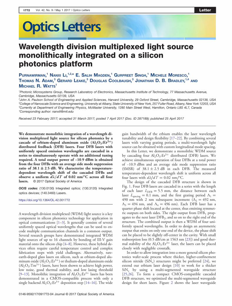
In order to allow integration into a more general silicon pho-tonics wafer-scale process where thicker, higher-confinementsilicon nitride (SiNx) structures might be preferred [24], weextend our erbium laser design [10] to work for a thickerSiNx by using a multi-segmented waveguide structure[25,26]. To form a compact CMOS-compatible cascadedDFB structure, we optimized the multi-segmented waveguidedesign for short lasers. Figure 2 shows the laser waveguide
1772 Vol. 42, No. 9 / May 1 2017 / Optics Letters Letter
0146-9592/17/091772-04 Journal © 2017 Optical Society of America
which consists of nitride (SiNx) segments with the grating per-turbation formed by periodic etching of the first and lastsegments. The SiNx segments have dimensions of thicknesst � 200 nm, width w � 450 nm, and gap g � 400 nm. A sil-icon dioxide (SiO2) gap gox � 200 nm is then added on top ofthe SiNx structure. All fabrication steps until SiO2 cladding arecompleted in a 300 mm line CMOS foundry, as reported ear-lier [10], only with a difference in layer thickness. Lastly, theAl2O3:Er
3� gain medium of thickness tAlO � 1100 nm isdeposited by a reactive co-sputtering process [23,27] as thefinal backend step. The Er3� ion concentration is N Er �1.0 × 1020 cm−3, and the background loss is measured to be<0.1 dB∕cm, using the prism coupling method.
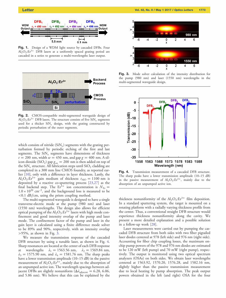
The multi-segmented waveguide is designed to have a singletransverse-electric mode at the pump (980 nm) and laser(1550 nm) wavelengths. The design also allows for efficientoptical pumping of the Al2O3:Er
3� lasers with high mode con-finement and good intensity overlap of the pump and lasermode. The confinement factor of the pump and laser in thegain layer is calculated using a finite difference mode solverto be 89% and 90%, respectively, with an intensity overlap>95%, as shown in Fig. 3.
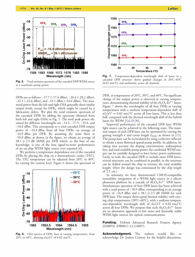
We measure the transmission response of the cascadedDFB structure by using a tunable laser, as shown in Fig. 4.Sharp resonances are located at the center of each DFB responseat wavelengths λ1 � 1563.56 nm, λ2 � 1569.84 nm,λ3 � 1575.90 nm, and λ4 � 1581.76 nm. The sharp peakshave a lower transmission amplitude (10–15 dB) in the passivemeasurement of Al2O3:Er
3�, mainly due to the absorption ofan unpumped active ion. The wavelength spacings between ad-jacent DFBs are slightly nonuniform (Δλadjacent � 6.28, 6.06,and 5.86 nm). We believe that this can be explained by the
thickness nonuniformity of the Al2O3:Er3� film deposition.
In a standard sputtering system, the target is mounted on arotating platform with a radially varying thickness profile fromthe center. Thus, a conventional straight DFB structure wouldexperience thickness nonuniformity along the cavity. Wepresent a more detailed explanation and a possible solutionin a follow-up work [28].
Laser measurements were carried out by pumping the cas-caded DFB structure from both sides with two fiber pigtailedlaser diodes centered at 978 (left side) and 976 nm (right side).Accounting for fiber chip coupling losses, the maximum on-chip pump powers of the 978 and 976 nm diodes are estimatedto be 120 mW (left pump) and 70 mW (right pump), respec-tively. The output is monitored using two optical spectrumanalyzers (OSAs) on both sides. We obtain laser wavelengthscentered at 1563.92, 1570.20, 1576.28, and 1582.16 nm,slightly higher than the passive transmission measurementdue to local heating by pump absorption. The peak outputpowers obtained in the left (and right) OSA for the four
Fig. 1. Design of a WDM light source by cascaded DFBs. FourAl2O3:Er
3� DFB lasers at a uniformly spaced grating period arecascaded in a series to generate a multi-wavelengths laser output.
Fig. 2. CMOS-compatible multi-segmented waveguide design ofAl2O3:Er
3� DFB lasers. The structure consists of five SiNx segmentsused for a thicker SiNx design, with the grating constructed byperiodic perturbation of the outer segments.
Fig. 3. Mode solver calculation of the intensity distribution forthe pump (980 nm) and laser (1550 nm) wavelengths in themulti-segmented waveguide design.
Fig. 4. Transmission measurement of a cascaded DFB structure.The sharp peaks have a lower transmission amplitude (10–15 dB)in the passive measurement of Al2O3:Er
3�, mainly due to theabsorption of an unpumped active ion.
Letter Vol. 42, No. 9 / May 1 2017 / Optics Letters 1773
DFBs are as follows: −17.7 (−17.4 dBm), −20.4 (−20.2 dBm),−22.1 (−22.6 dBm), and −19.1 dBm (−24.0 dBm). The mea-sured power from the left and right OSA generally show similaroutput levels, except for DFB4, which might be caused by afabrication defect. We plot the total emission spectrum ofthe cascaded DFBs by adding the spectrum obtained fromboth left and right OSAs in Fig. 5. The total peak power ob-tained for different wavelengths are −14.5, −17.5, −19.4, and−18.0 dBm. This corresponds to a total cascaded DFB outputpower of −10.9 dBm from all four DFBs, an average of−16.9 dBm per DFB. By assuming the noise floor at−55.0 dBm, as shown in the figure, we obtain an average of38.1� 2.5 dB SMSR per DFB which, to the best of ourknowledge, is one of the best signal-to-noise performancesof an on-chip WDM light source ever reported [6].
We perform a temperature dependence test of the cascadedDFBs by placing the chip on a thermoelectric cooler (TEC).The TEC temperature can be adjusted from 20°C to 40°Cby varying the current level. Figure 6 shows the spectrum of
DFB1 at temperatures of 20°C, 30°C, and 40°C. No significantchange of the output power is observed at varying tempera-tures, demonstrating thermal stability of the Al2O3:Er
3� lasers.Figure 7 shows the wavelengths of all four DFBs at varyingtemperatures with a uniform temperature-dependent shift ofdλ∕dT � 0.02 nm∕°C across all four lasers. This is less thanhalf, compared with the thermal wavelength shift of the hybridlasers for WDM [5,6,29,30].
Improved performance of the cascaded DFB laser WDMlight source can be achieved in the following ways. The maxi-mal output of each DFB laser can be optimized by varying thegrating strength κ and cavity length LDFB, as shown in [15].The pump laser can be recirculated by using a selective reflectorto obtain a more flattened spatial pump profile. In addition, bytaking into account the doping concentration, reabsorptionloss, and total available pump power, the combined WDMout-put can be carefully designed to have better power uniformity.Lastly, to scale the cascaded DFB to include more DFB lasers,several structures can be combined in parallel, or the structurecan be folded around the chip to increase the total availablelength. (Here the design was constrained by the chip lengthof 2.5 cm.)
In summary, we have demonstrated CMOS-compatiblemonolithic integration of a WDM light source in a siliconphotonics platform by a cascade of Al2O3:Er
3� DFB lasers.Simultaneous operation of four DFB lasers has been achievedwith a total power of −10.9 dBm, corresponding to an averagepower of −16.9 dBm and a 38.1� 2.5 dB SMSR for eachDFB laser. The output shows good thermal stability with vary-ing chip temperatures (20°C–40°C), with a uniform tempera-ture-dependent wavelength shift of dλ∕dT � 0.02 nm∕°Cacross all four DFBs. We propose that such Al2O3:Er
3� lasersare an alternative approach to low noise and thermally stableWDM light sources for optical communications.
Funding. Defense Advanced Research Projects Agency(DARPA) (HR0011-12-2-0007).
Acknowledgment. The authors would like toacknowledge Dr. Joshua Conway for the helpful discussions.
Fig. 5. Total emission spectrum of the cascaded DFBWDM sourceat a maximum pump power.
Fig. 6. OSA spectra of DFB1 laser at varying temperatures, from20°C to 40°C, showing dλ∕dT of 0.02 nm/°C.
Fig. 7. Temperature-dependent wavelength shift of lasers in acascaded DFB structure shows gradual changes in 20°C–40°C(0.02 nm/°C) and uniformity across all channels.
1774 Vol. 42, No. 9 / May 1 2017 / Optics Letters Letter
N. Li is sponsored by National Science Scholarship (NSS) fromthe Agency of Science, Technology and Research (A*STAR),Singapore.
REFERENCES
1. M. J. R. Heck, J. F. Bauters, M. L. Davenport, J. K. Doylend, S. Jain,G. Kurczveil, S. Srinivasan, Y. B. Tang, and J. E. Bowers, IEEE J. Sel.Top. Quantum Electron. 19, 6100117 (2013).
2. L. Stampoulidis, K. Vyrsokinos, K. Voigt, L. Zimmermann, F.Gomez-Agis, H. J. S. Dorren, Z. Sheng, D. Van Thourhout, L.Moerl, J. Kreissl, B. Sedighi, J. C. Scheytt, A. Pagano, and E.Riccardi, IEEE J. Sel. Top. Quantum Electron. 16, 1422 (2010).
3. M. J. R. Heck, H. W. Chen, A. W. Fang, B. R. Koch, D. Liang, H. Park,M. N. Sysak, and J. E. Bowers, IEEE J. Sel. Top. Quantum Electron.17, 333 (2011).
4. A. Alduino, L. Liao, R. Jones, M. Morse, B. Kim, W.-Z. Lo, J. Basak, B.Koch, H.-F. Liu, H. Rong, M. Sysak, C. Krause, R. Saba, D. Lazar, L.Horwitz, R. Bar, S. Litski, A. Liu, K. Sullivan, O. Dosunmu, N. Na, T.Yin, F. Haubensack, I.-W. Hsieh, J. Heck, R. Beatty, H. Park, J.Bovington, S. Lee, H. Nguyen, H. Au, K. Nguyen, P. Merani, M.Hakami, and M. Paniccia, Integrated Photonics Research, Siliconand Nanophotonics (IPRSN) (2010).
5. S. S. Sui, M. Y. Tang, Y. D. Yang, J. L. Xiao, Y. Du, and Y. Z. Huang,IEEE J. Quantum Electron. 51, 1 (2015).
6. S. Tanaka, S. H. Jeong, S. Sekiguchi, T. Akiyama, T. Kurahashi, Y.Tanaka, and K. Morito, in Optical Fiber Communication Conferenceand Exposition and the National Fiber Optic Engineers Conference(IEEE, 2013).
7. L. Tao, L. Yuan, Y. Li, H. Yu, B. Wang, Q. Kan, W. Chen, J. Pan, G.Ran, and W. Wang, Opt. Express 22, 5448 (2014).
8. G. Kurczveil, M. J. R. Heck, J. D. Peters, J. M. Garcia, D. Spencer, andJ. E. Bowers, IEEE J. Sel. Top. Quantum Electron. 17, 1521 (2011).
9. N. Li, Purnawirman, Z. Su, E. Salih Magden, P. T. Callahan, K.Shtyrkova, M. Xin, A. Ruocco, C. Baiocco, E. P. Ippen, F. X.Kärtner, J. D. B. Bradley, D. Vermeulen, and M. R. Watts , Opt. Lett.42, 1181 (2017).
10. E. S. Hosseini, Purnawirman, J. D. B. Bradley, J. Sun, G. Leake, T. N.Adam, D. D. Coolbaugh, and M. R. Watts, Opt. Lett. 39, 3106 (2014).
11. E. H. Bernhardi, H. van Wolferen, L. Agazzi, M. R. H. Khan, C. G. H.Roeloffzen, K. Worhoff, M. Pollnau, and R. M. de Ridder, Opt. Lett. 35,2394 (2010).
12. M. Belt and D. J. Blumenthal, in Optical Fiber CommunicationsConference and Exhibition (2015), pp. 1–3.
13. Z. Su, N. Li, E. Salih Magden, M. Byrd, Purnawirman, T. N. Adam, G.Leake, D. Coolbaugh, J. D. B. Bradley, and M. R. Watts, Opt. Lett. 41,5708 (2016).
14. G. Singh, Purnawirman, J. D. B. Bradley, N. Li, E. S. Magden, M.Moresco, T. N. Adam, G. Leake, D. Coolbaugh, and M. R. Watts,Opt. Lett. 41, 1189 (2016).
15. M. Belt and D. J. Blumenthal, Opt. Express 22, 10655 (2014).16. E. S. Magden, Purnawirman, N. Li, G. Singh, J. D. B. Bradley, G. S.
Petrich, G. Leake, D. D. Coolbaugh, M. R. Watts, and L. A.Kolodziejski, “Fully CMOS-compatible integrated distributed feedbacklaser with 250°C fabricated Al2O3:Er3+ gain medium,” inConference onLasers and Electro-Optics (CLEO), San Jose, California, OpticalSociety of America, 2016, paper SM1G.2.
17. Y. Liu, K.Wu, N. Li, L. Lan, S. Yoo, X.Wu, P. P. Shum, S. Zeng, and X.Tan, J. Opt. Soc. Korea 17, 357 (2013).
18. N. J. C. Libatique, L. Wang, and R. K. Jain, Opt. Express 10, 1503(2002).
19. N. Li, E. Timurdogan, C. V. Poulton, M. Byrd, E. S. Magden, Z. Su,Purnawirman, G. Leake, D. D. Coolbaugh, D. Vermeulen, and M. R.Watts, Opt. Express 24, 22741 (2016).
20. Y. W. Song, S. A. Havstad, D. Starodubov, Y. Xie, A. E. Willner, and J.Feinberg, IEEE Photon. Technol. Lett. 13, 1167 (2001).
21. J. H. Wong, H. Q. Lam, S. Aditya, J. Zhou, N. Li, J. Xue, P. H. Lim, K.E. K. Lee, K. Wu, and P. P. Shum, J. Lightwave Technol. 30, 3164(2012).
22. F. Xiao, K. Alameh, and T. Lee, Opt. Express 17, 18676 (2009).23. K. Worhoff, J. D. B. Bradley, F. Ay, D. Geskus, T. P. Blauwendraat,
and M. Pollnau, IEEE J. Quantum Electron. 45, 454 (2009).24. A. Gondarenko, J. S. Levy, and M. Lipson, Opt. Express 17, 11366
(2009).25. Purnawirman, E. S. Hosseini, J. Sun, T. N. Adam, G. Leake, D. D.
Coolbaugh, M. R. Watts, and A. Baldycheva, in Optical FiberCommunication Conference, San Francisco, California, 2014, paperW4E.5.
26. C. M. Sorace-Agaskar, P. T. Callahan, K. Shtyrkova, A. Baldycheva, M.Moresco, J. Bradley, M. Y. Peng, N. Li, E. S. Magden, P. Purnawirman,M. Y. Sander, G. Leake, D. Coolbaugh, M. R. Watts, and F. Kartner,“Integrated mode-locked lasers in a CMOS-compatible silicon photonicplatform,” in Conference on Lasers and Electro-Optics (CLEO), SanJose, California, Optical Society of America, 2015, paper SM2I.5.
27. J. D. Bradley, Z. Su, E. S. Magden, N. Li, M. Byrd, Purnawirman, T. N.Adam, G. Leake, D. Coolbaugh, and M. R. Watts, Proc. SPIE 9744,97440U (2016).
28. Purnawirman, “Integrated erbium lasers in silicon photonics,”Ph.D. dissertation (Massachusetts Institute of Technology, 2017).
29. S. Tanaka, S.-H. Jeong, S. Sekiguchi, T. Kurahashi, Y. Tanaka, andK. Morito, Opt. Express 20, 28057 (2012).
30. J. Seok-Hwan, T. Shinsuke, S. Shigeaki, K. Teruo, H. Nobuaki, A.Suguru, U. Tatsuya, Y. Tsuyoshi, A. Tomoyuki, T. Yu, and M. Ken,Jpn. J. Appl. Phys. 51, 082101 (2012).
Letter Vol. 42, No. 9 / May 1 2017 / Optics Letters 1775