Embed Size (px)
Citation preview
Wafer-Level Micro-Optics: Trends in Manufacturing, Testing and Packaging
Reinhard Voelkeli, Kenneth J. Weible, Martin Eisner
SUSS MicroOptics SA, Jaquet-Droz 7, CH-2000 Neuchâtel, Switzerland, www.suss.ch
ABSTRACT
Micro-optics is an indispensable key enabling technology (KET) for many applications today. The important role of micro-optical components is based on three different motivations: miniaturization, high functionality and packaging aspects. It is obvious that miniaturized systems require micro-optics for light focusing, light shaping and imaging. More important for industrial applications is the high functionality of micro-optics that allows combining these different functions in one element. In DUV Lithography Steppers and Scanners an extremely precise beam shaping of the Excimer laser profile is required. High-precision diffractive optical elements are well suited for this task. For Wafer-Level Cameras (WLC) and fiber optical systems the packaging aspects are more important. Wafer-Level Micro-Optics technology allows manufacturing and packaging some thousands of sub-components in parallel. We report on the state of the art in wafer-based manufacturing, testing and packaging.
Keywords: Micro-optics, microlens array, diffractive optical elements, wafer-level optics, wafer-level packaging, beam shaping, fiber coupling, array illumination, Shack-Hartmann, confocal microscope, slow-axis collimator.
1 INTRODUCTION Micro-optics is regarded as a relatively novel technology. Most research institutes dealing with micro-optics were established in the 1980s or 90s. The first companies for manufacturing micro-optics were founded about 10 years later as spin-off from these research institutes. Still today the supplier’s base for micro-optics is relatively small. Micro-optics remains to be a niche product, not a big business. Micro-optical elements are refractive, diffractive, reflective or hybrid optics. Diffraction, scattering and interference effects at micro-optical elements could be quite complex: Moiré effects in stacked microlens arrays, intensity modulation in laser beam shapers, ghost images of diffractive optical elements, speckles – only some of the possible problems using micro-optics. In addition, the standard optical design software often does not allow simulating and modeling the optical properties of these elements correctly. Micro-optics requires special metrology tools for characterization and testing. System integration follows different rules than the classical optical components like lenses, prisms, beam splitters, etc.. The overall performance of a device using micro-optical components is often not exactly predictable during the design phase. Thus, micro-optics remains somewhat “exotic” for many optical designers and engineers.
But, micro-optics has much to offer. Micro-optics allows to precisely shaping illumination light for imaging and projection system. Micro-optical fiber couplers, gratings for wavelength multiplexing and switches are essential key components for high-speed communication systems. Micro-optics allows to manufacture thousands of high-quality miniaturize systems on one wafer at very attractive costs. Endoscopes using graded-index microlenses have enabled micro-invasive surgery. The list of examples where micro-optics is an indispensable key component is long. Interestingly this is not such a new phenomenon. Already some hundred years ago researchers invented devices and systems based on micro-optics. Most of these inventions failed, because no suitable manufacturing technology for the micro-optics was available. In the following we will explain how semiconductor industry finally allowed manufacturing micro-optics with high precision. We will report on recent trends in wafer-level optics manufacturing, testing and packaging and present typical applications.
i [email protected], +41-32-7205103, www.suss.ch, www.suss.com
Invited Paper
Optical Fabrication, Testing, and Metrology IV, edited by Angela Duparré, Roland Geyl, Proc. of SPIE Vol. 816981690C · © 2011 SPIE · CCC code: 0277-786X/11/$18 · doi: 10.1117/12.897114
Proc. of SPIE Vol. 8169 81690C-1
Downloaded from SPIE Digital Library on 01 Oct 2011 to 212.147.28.244. Terms of Use: http://spiedl.org/terms
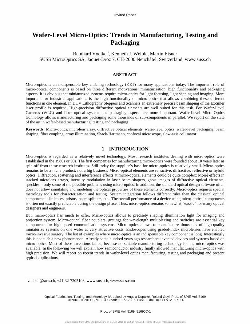
2 THE HISTORY OF MICRO-OPTICS First micro-optical elements were manufactured by Antonie van Leeuwenhoek (1632 – 1723), a pioneer of microscopy and microbiology. Leeuwenhoek melted small rods of soda lime glass in a hot flame to obtain high-quality glass spheres. These ball lenses improved the resolution of his microscope viewers beyond current limits. He was the first to observe and report about single-cell micro-organisms. Another pioneer of microscopy, Robert Hooke (1635 – 1703), published his famous book “Micrographia”, a collection of microscope observations, in 1665. Amongst them is the fascinating drawing of a fly’s compound eye shown in Figure 1 (left), a natural microlens array. In fact, first natural microlens arrays appeared already in the Early Cambrian period, some 500 million years ago. Trilobites, a fossil group of marine arthropods, had complex compound eyes with microlenses made of calcite. Still today, similar compound eyes are found in many small creatures. Microlens arrays seem to be the appropriate solution for miniaturized vision systems in Nature.
Figure 1. (left) Image of a fly’s eye from Micrographia by Robert Hooke, 1665; (center) enlarged view of cylindrical
microlens array on a photographic plate for integral photography, proposed by Walter Hess, 1912 [4]; (right) fly’s eye condenser for illuminating a film with uniform light as proposed by Mihalyi in 1927 [5].
The development of man-made micro-optics is much connected with photo- and cinematography. In 1891, Gabriel Lippmann (1845 – 1921) invented “interference color photography” [1]. He fixed a mirror in contact to the photographic emulsion and recorded the interference pattern from incident and reflected light in a sensitive but transparent emulsion. The Lippmann color photos, later referred as Lippmann holograms, were in fact first wavelength-selective volume holograms. For white light illumination, constructive and destructive interference generated the color image in reflection. Astonishingly, this invention was made without laser and long before Denis Gabor invented the holography in 1948 [2].
Lippmann also invented the “integral photography” an auto-stereoscopic method to display 3D images for observation with the naked eye [3]. Integral photography uses an array of small microlenses to record multiple sub-images of a scene in a photographic layer. Each microlens acted like a miniaturized camera recording an individual sub-image. Observing the developed photo plate through a similar lens array, the superimposed sub-images form an auto-stereoscopic integral image, a 3D image. In 1912 Walter Hess [4] proposed to use an array of cylindrical microlenses as shown in Figure 1 (center). These 3D displays based on cylindrical microlens arrays are later referred as parallax panoramagrams. Today’s 3D postcards and most of the new 3D television screens are based on this principle. Another important field of applications for microlens arrays is fly’s eye condensers, also referred as Köhler integrators, providing a uniform illumination for color slide or film projector. Figure 1 (right) shows a Köhler integrator, consisting of two microlens arrays at a focal-length distance, for illumination of color film projectors, as proposed by Joseph Mihalyi in 1927 [5].
Over the last hundred years, many researchers published and patented inventions where refractive or diffractive array optics was the decisive key element for light shaping or imaging. Often brilliant ideas, but only few of them could be realized and even fewer were a commercial success. For the early micro-optics applications the insurmountable entrance barrier was the availability of suitable micro-optical elements for reasonable costs. In the early days, microlens arrays or grating were engraved or polished for example, on a lathe. This piece-by-piece manufacturing was too time-consuming and very expensive. Later, glass molding and pressing was used, for example, to manufacture fly’s eye condensers for slide and film projections. The quality of these microlens arrays remained often poor. Surface roughness, defects, lens profile accuracy and non-uniformities in the array constrained their field of applications to illumination tasks. For more sophisticated applications, requiring, for example, two or three micro-optics layers, the lateral mismatch (grid imperfections) and the array-to-array alignment were often problematic. Thus, using micro-optics was considered to be an exotic idea, but usually did not lead to success. This situation changed with the rapid progress of micro-structuring technology in the second part of the last century.
Proc. of SPIE Vol. 8169 81690C-2
Downloaded from SPIE Digital Library on 01 Oct 2011 to 212.147.28.244. Terms of Use: http://spiedl.org/terms
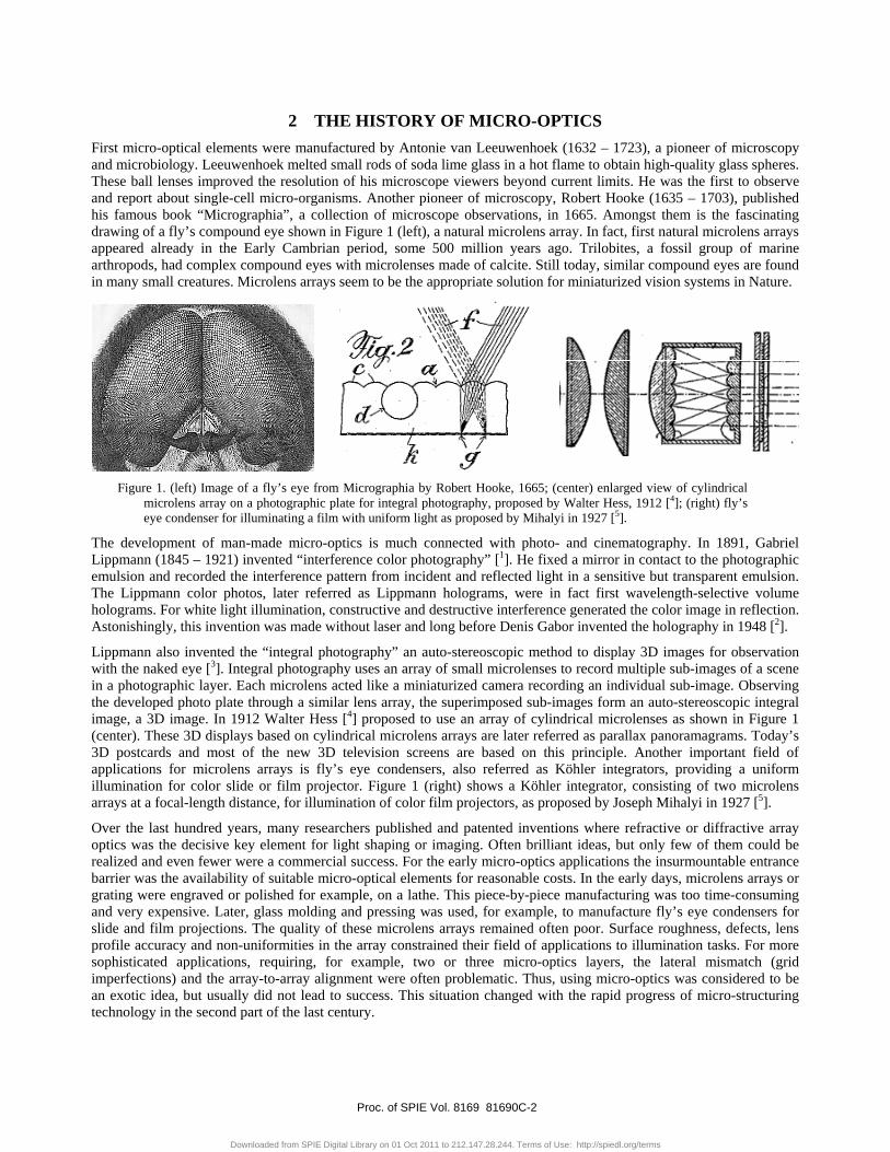
3 THE PLANAR PROCESS In the early days of electronics, vacuum tubes, later discrete Germanium transistors were used for radio receivers. In electronics, the breakthrough came in 1959, when Robert Noyce and Jean Hoerni started to manufacture integrated circuits (IC) on planar silicon substrates, the first wafers. Jean Hoerni micro-structured planar wafers by using photosensitive resist, a photomask, a wet-chemical development process and subsequent metal deposition, etching or diffusion processes [6]. This so-called “planar process” shown schematically in Figure 2 (left) now allowed to mass-produce miniaturized transistors and to integrate many of them in one microchip. Hundreds, thousands and later millions of electronics components could be manufactured in parallel. Replacing a discrete piece-by-piece manufacturing of transistors by the highly-parallel planar process was the big-bang for semiconductor industry.
Figure 2. (left) The planar process for manufacturing multiple transistors on a planar wafer as proposed by Jean Hoerni
in 1959 [6]; (center) multi-level diffractive optical elements manufactured with a planar process as proposed by Mike Gale in 1977 [7]; (right) 8-level diffractive optical element for beam shapingii.
The planar process could also be used for the manufacturing of micro-optics on wafer-level. Mike Gale et. al. manufactured multi-level diffractive optical elements on wafer-level in 1977 [7]. As shown in Figure 2 (center), a 4-level diffractive optical element is achieved by two subsequent photolithography and etching steps. The combination of computer generated hologram (CGH), invented by Adolf W. Lohmann et. al. in 1966 [8], with the planar process allowed to generate highly efficient diffractive optical elements (DOE) for light shaping.
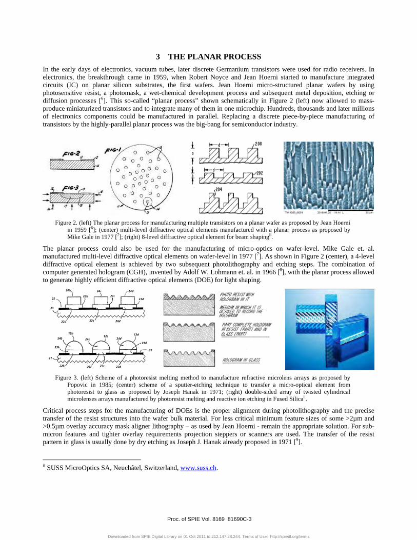
Figure 3. (left) Scheme of a photoresist melting method to manufacture refractive microlens arrays as proposed by
Popovic in 1985; (center) scheme of a sputter-etching technique to transfer a micro-optical element from photoresist to glass as proposed by Joseph Hanak in 1971; (right) double-sided array of twisted cylindrical microlenses arrays manufactured by photoresist melting and reactive ion etching in Fused Silicaii.
Critical process steps for the manufacturing of DOEs is the proper alignment during photolithography and the precise transfer of the resist structures into the wafer bulk material. For less critical minimum feature sizes of some >2µm and >0.5µm overlay accuracy mask aligner lithography – as used by Jean Hoerni - remain the appropriate solution. For sub-micron features and tighter overlay requirements projection steppers or scanners are used. The transfer of the resist pattern in glass is usually done by dry etching as Joseph J. Hanak already proposed in 1971 [9].
ii SUSS MicroOptics SA, Neuchâtel, Switzerland, www.suss.ch.
Proc. of SPIE Vol. 8169 81690C-3
Downloaded from SPIE Digital Library on 01 Oct 2011 to 212.147.28.244. Terms of Use: http://spiedl.org/terms

In 1985, Popovic et. al. developed a microlens manufacturing technology which is based on micro-structuring of photoresist by photolithography and a subsequent resist melting process [10], shown in Figure 3 (left). Reactive ion etching (RIE) is used to transfer the resist microlens into durable hard glass materials.
4 WAFER-LEVEL MANUFACTURING OF MICRO-OPTICAL ELEMENTS Many alternative technologies like grinding, ultrasonic lapping, diamond drilling and cutting, ion-diffusion, etching, laser ablation, casting, embossing, molding, LIGA, ion-implanting, photo-structurable glass, etc. have been developed for manufacturing of micro-optics. However, none of these technologies has achieved the high level of wafer-based technologies. As discussed in the previous chapter, this is much related to semiconductor industry, who has improved the original “planar process” of Jean Hoerni far beyond all imaginable limits. Wafer-optics manufacturing on research-level typically rests upon 100mm wafer technology, whereas industrial manufacturing is usually based on 150mm and 200mm technology. This choice is much related to the cost of owning and operating equipment. 100mm equipment has been phased out by semiconductor industry end of the 1980s. The move to 150mm also provided leading-edge lithography tools being able to print features below 500nm with an overlay better than 50nm. The transition to 200mm was made around 1998, since 2004 the 300mm wafer-technology is the standard in semiconductor industry.
Probably the best choice for wafer-based manufacturing of micro-optics is 200mm technology. This is again related to semiconductor manufacturing trends. Whereas most ancient 100mm and 150mm semiconductor fabs have disappeared, the 200mm fabs remained in full operation, even after the transition to 300mm. For example, old 200mm DRAM fabs are now used for mass-production of CMOS image sensors and MEMS devices. This is a strong argument to opt for 200mm micro-optics technology. Equipment manufacturer remain interested to update their 200mm tools and novel technology trends, like wafer-level packaging (WLP), thin-wafer-handling and TSV/3D-IC, are also made available for 200mm equipment.
4.1 Wafer Cleaning and Photoresist Coating
The wafer processing starts with wet cleaning. Typically this is done by a pre-cleaning, a piranha etch, a mixture of sulfuric acid (H2SO4) and hydrogen peroxide (H2O2), to remove organic contamination; and spin rinse drying. Additional ultra- or mega-sonic cleaning, brush cleaning, high-pressure water jet or plasma cleaning might be used. For non-conductive wafer materials like Borofloat and Fused Silica, the plasma cleaning process shows a significant drawback. The plasma activates the wafer surface, which is very useful for wafer bonding, but also attracts electrically charged particles from air. Especially for manufacturing of defect-free arrays the cleaning process is very crucial for the yield.
For manufacturing of diffractive optical elements (DOE), the required photoresist thickness ranges from some 20nm to several microns. Thus, a thin resist layer is spin-coated and patterned by photolithography and wet-chemical resist development. This is usually a very uncritical process for a single layer. For multi-level DOEs, as shown in Figure 2 (center) and Figure 5, additional resist layers have to be coated on top of the previous layers. Here the coating process is more critical, as the new resist layer has to cover the pre-structured wafer topography completely.
For refractive optical elements (ROE), the required resist layer thickness ranges from some microns to more than 100µm layers. Fully automatic spin coaters, like SUSS MicroTec ACS200iv, ensure a high repeatability of the coating process. For glass wafers, edge-handling tooling is used to improve the uniformity. For the melting resist technology shown in Figure 3 (left), the uniformity of the resist layer is directly related to the uniformity of the microlenses after melting. Thus, a wafer mapping of the resist allows monitoring quality at an early stage of the manufacturing process.
Automatic non-contact measurement tools, like the KT22 from Foothilliii, allow monitoring the resist thickness with better than 1nm accuracy over the full wafer. Figure 4 shows the mapping of the resist uniformity for a 200mm wafer coated with 50µm thick photoresist by spin-coating in SUSS MicroTec ASC200iv. An excellent resist uniformity of 0.25% (rms) and 0.82% (p-v) is measured for 160mm test area in KT22iii film thickness measurement tool.
iii KT22 film thickness tool from Foothill Instruments LLC, www.foothill-instruments.com iv SUSS MicroTec AG, Garching, Germany, www.suss.com
Proc. of SPIE Vol. 8169 81690C-4
Downloaded from SPIE Digital Library on 01 Oct 2011 to 212.147.28.244. Terms of Use: http://spiedl.org/terms

Figure 4. Mapping of the resist uniformity for 200mm wafer coated with 50µm thick photoresist by spin-coating in
SUSS MicroTec ASC200. An excellent resist uniformity of 0.25% (rms) and 0.82% (p-v) is measured for 160mm test area in KT22 film thickness measurement tool.
4.2 Photolithography for Diffractive Optical Elements (DOE)
Today, leading-edge immersion lithography steppers allow to print structures down to some 22 nanometers on 300mm wafers in mass-production. Compared to semiconductor industry, the lithography requirements for micro-optics are much more relaxed. Typically a minimum feature size of 0.5 to 0.8µm is sufficient for diffractive optical elements (DOE). Thus, older and much less expensive 365nm-stepper technology from the 1990s is well suited for this task. More important for DOEs is the overlay accuracy, the step height and grid errors in larger gratings. Figure 5 (left) shows the SEM picture of an 8-level diffractive optical (intersection of three Fresnel lenses in hexagonal package) manufactured with i-line stepper and RIE transfer in Fused Silica.
Figure 5. (left) SEM picture of 8-level diffractive optical element (DOE) for beam shaping; (right) an overlay mismatch
of ≈40nm (arrow) is visible in SEM, but uncritical for optical performance at 193nm wavelength.
Figure 5 (right) shows an overlay mismatch on the order of 40nm from one 4th to 5th level (arrow). For most optical applications overlay errors <50nm do not affect the optical performance of a DOE in a measurable way.
4.3 Photolithography and Resist Melting for Refractive Microlenses
Due to a very limited depth-of-focus, projection lithography tools are not well suited for thick resist exposure. Thus mask aligners in contact or proximity mode are the preferred lithography tool. Contact lithography allows resolving fine details, but requires particle-free surfaces and frequent mask cleaning. In production, mask aligners are usually used in proximity mode, whereas the mask is at a distance of some 10 to 30µm above the wafer. Thick film photoresists, like AZ
Proc. of SPIE Vol. 8169 81690C-5
Downloaded from SPIE Digital Library on 01 Oct 2011 to 212.147.28.244. Terms of Use: http://spiedl.org/terms
4562v, AZ 9260v or AZ 40XTv, are optimized for mask aligner lithography. Some thick resists even show a light guiding characteristic during the exposure process: Exposed areas become transparent and guide the exposure light linearly in deeper resist regions. Typically an aspect ratio of 5 to 7 is achieved with good sidewalls for thick resist. Consequently, for a 50µm thick resist layer a lens-to-lens gap of some 7µm is required to avoid deformation of the lens profile during the resist melting process.
Recently mask aligner lithography was significantly improved by a novel illumination system referred as MO Exposure Optics [11]. MO Exposure Optics improves the uniformity of the illumination light, provides telecentric illumination and allows reducing diffraction effects by shaping the angular spectrum of the mask illuminating light (customized illumination. Now, photolithography enhancement techniques, like optical proximity correction (OPC) and source mask optimization (SMO), are applicable in mask aligner lithography. Especially for thick resist lithography these techniques allow to further improve resolution and CD uniformity for proximity lithography beyond today’s limits.
After wet-chemical development and drying, the resist structures are melted in an oven or on a hot-plate at temperatures around 150 to 180ºC. The melting procedure itself is quite simple [12]. Above the softening temperature the edges of the resist structure start melting. Above the glass transition temperature the amorphous resist polymer changes into a glass state system. The surface tension tries to minimize the surface area by rearranging the liquid masses inside the drop. Ideally, the resist melts completely, the masses are freely transported and surface tension forms a spherical microlens. In practice, the lens melting process needs careful process optimization and precise control of all process parameters to obtain good lens-to-lens uniformity within one wafer and from wafer-to-wafer. Repeatability and uniformity of melted resist lenses are key factors for the following etch process.
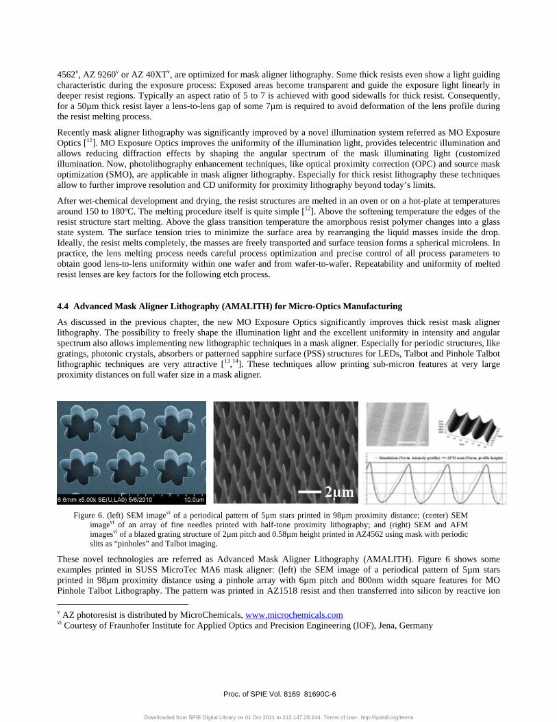
4.4 Advanced Mask Aligner Lithography (AMALITH) for Micro-Optics Manufacturing
As discussed in the previous chapter, the new MO Exposure Optics significantly improves thick resist mask aligner lithography. The possibility to freely shape the illumination light and the excellent uniformity in intensity and angular spectrum also allows implementing new lithographic techniques in a mask aligner. Especially for periodic structures, like gratings, photonic crystals, absorbers or patterned sapphire surface (PSS) structures for LEDs, Talbot and Pinhole Talbot lithographic techniques are very attractive [13,14]. These techniques allow printing sub-micron features at very large proximity distances on full wafer size in a mask aligner.
Figure 6. (left) SEM imagevi of a periodical pattern of 5µm stars printed in 98µm proximity distance; (center) SEM
imagevi of an array of fine needles printed with half-tone proximity lithography; and (right) SEM and AFM imagesvi of a blazed grating structure of 2µm pitch and 0.58µm height printed in AZ4562 using mask with periodic slits as “pinholes” and Talbot imaging.
These novel technologies are referred as Advanced Mask Aligner Lithography (AMALITH). Figure 6 shows some examples printed in SUSS MicroTec MA6 mask aligner: (left) the SEM image of a periodical pattern of 5µm stars printed in 98µm proximity distance using a pinhole array with 6µm pitch and 800nm width square features for MO Pinhole Talbot Lithography. The pattern was printed in AZ1518 resist and then transferred into silicon by reactive ion v AZ photoresist is distributed by MicroChemicals, www.microchemicals.com vi Courtesy of Fraunhofer Institute for Applied Optics and Precision Engineering (IOF), Jena, Germany
Proc. of SPIE Vol. 8169 81690C-6
Downloaded from SPIE Digital Library on 01 Oct 2011 to 212.147.28.244. Terms of Use: http://spiedl.org/terms

etching (Bosch process). Figure 6 (center) shows an array of fine needles with 2µm pitch printed with half-tone proximity lithography at 10µm proximity distance. Figure 6 (right) shows SEM and AFM images of a blazed grating structure of 2µm pitch and 0.58µm height printed in AZ4562 using a slit mask and Talbot imaging.
4.5 Reactive Ion Etching (RIE)
In the next step the resist structures are transferred into the bulk wafer material by plasma ion etching. For wafer processing reactive ion etching (RIE), where the effects of the ion bombardment is enhanced by reactive gases like SF6 and CHF3, is the preferred choice. The etching process removes atoms from the resist and wafer surface at different etch rates. Surface areas covered by resist structures are protected until the covering resist layer is removed. Typical etch rates range from less than 0.01µm/min to about 1µm/min depending on the ion energy and the reactive etch gases in the plasma chamber. Slow etch rates are preferred for diffractive optical elements with only small etch depths. For the transfer of refractive resist lenses a faster etching process is preferred to reduce the total etching time.
The optical performance of a DOE is determined by the diffraction efficiency and the noise level, i.e. the percentage of light in 0th order, spurious orders and ghost images. To obtain a high optical performance a correct etch depth on the order of λ/20 is required. Figure 7 shows (left) the phase profile of 16-level diffractive optical elements for focus spot generation, measured in white light profilometer Wyko NT3300vii; and (right) a scan of the x-profile from same measurement showing a total phase depth of 320nm sub-dived to 16 phase levels. A diffraction efficiency of 98% and less than 0.1% in the 0th diffraction order was achieved for a 16-level DOE shown in Figure 7.
Figure 7. Phase profile of a densely packed array of 16-level diffractive optical elements for focus spot generation,
measured in white light profilometer Wyko NT3300; (right) scan of x-profile from same measurement shows a total phase depth of 320nm sub-dived to 16 phase levels.
Melted resist lenses are usually very close to a spherical lens profile with a conic around k ≈ 0 after melting. The transfer of the melted resist lens by RIE allows changing this lens profile. This is done by varying the mixture of the etch gases and oxygen during the etch process. If the etch rate for resist is higher than for the wafer bulk material, the resulting lens profile will be flatter than the resist lens profile. A continuous change of all etch parameters allows to obtain aspherical lens profiles.
vii NT3300, Wyko, now www.bruker-axs.com
Proc. of SPIE Vol. 8169 81690C-7
Downloaded from SPIE Digital Library on 01 Oct 2011 to 212.147.28.244. Terms of Use: http://spiedl.org/terms

Figure 8. Comparison of measured lens profile (blue line) to ideal lens profile (dotted line) for a microlens of 1.08mm
lens diameter and 93µm sag height etched in Fused Silica.
Figure 8 shows the comparison of the measured lens profile (blue line) to the desired lens profile (dotted line) of a microlens with 1.08mm lens diameter and 93 µm lens sag height etched in Silica. The profile was measured in a KLA-Tencor P15viii mechanical profilometer. Figure 9 shows the deviation of the measured lens profile, expressed by a 12th degree polynomial fit, to the ideal lens profile. For a microlens of 1.08mm lens diameter, 93µm lens sag, 1.8mm radius of curvature and a conic constant of k = -1 a deviation of only 154.8nm (rms) is obtained.
Figure 9. Deviation of measured lens profile, expressed by a 12th degree polynomial fit, versus the ideal lens profile
shown in Figure 8. For a refractive microlens of 1.08mm lens diameter, 93µm lens sag, 1.8mm radius of curvature and a conic constant of k = -1 an excellent profile quality with only 154.8nm (rms) deviation is obtained.
Melting resist technology and subsequent reactive ion etching allows to manufacture aspherical microlenses with excellent profile accuracy and lens-to-lens uniformity on full wafer level. The described technology is based on planar wafer technology from semiconductor manufacturing and has been developed to a very high level. Excellent uniformity
viii P10, P15 mechanical stylus profilometer by KLA-Tencor, www.kla-tencor.com
Proc. of SPIE Vol. 8169 81690C-8
Downloaded from SPIE Digital Library on 01 Oct 2011 to 212.147.28.244. Terms of Use: http://spiedl.org/terms
for lens-to-lens and wafer-to-wafer allows providing high quality microlenses in hard durable material for very competitive pricing.
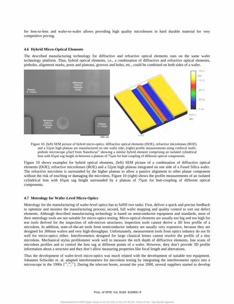
4.6 Hybrid Micro-Optical Elements
The described manufacturing technology for diffractive and refractive optical elements runs on the same wafer technology platform. Thus, hybrid optical elements, i.e., a combination of diffractive and refractive optical elements, pinholes, alignment marks, posts and plateaus, grooves and holes, etc., could be combined on both sides of a wafer.
Figure 10. (left) SEM picture of hybrid micro-optics: diffractive optical elements (DOE), refractive microlenses (ROE)
and a 52µm high plateau are manufactured on one wafer side; (right) profile measurements using confocal multi-pinhole microscope µSurf from Nanofocusix showing a similar hybrid element comprising an isolated cylindrical lens with 65µm sag height in-between a plateau of 75µm for butt coupling of different optical components.
Figure 10 shows examples for hybrid optical elements, (left) SEM picture of a combination of diffractive optical elements (DOE), refractive microlenses (ROE) and a 52µm high plateau integrated on one side of a Fused Silica wafer. The refractive microlens is surrounded by the higher plateau to allow a passive alignment to other planar component without the risk of touching or damaging the microlens. Figure 10 (right) shows the profile measurements of an isolated cylindrical lens with 65µm sag height surrounded by a plateau of 75µm for butt-coupling of different optical components.
4.7 Metrology for Wafer-Level Micro-Optics
Metrology for the manufacturing of wafer-level optics has to fulfill two tasks: First, deliver a quick and precise feedback to optimize and monitor the manufacturing process; second, full wafer mapping and quality control to sort out defect elements. Although described manufacturing technology is based on semiconductor equipment and standards, most of their metrology tools are not suitable for micro-optics testing. Micro-optical elements are usually too big and too high for test tools derived for the inspection of sub-micron structures; inspection tools cannot derive a 3D lens profile of a microlens. In addition, state-of-the-art tools from semiconductor industry are usually very expensive, because they are designed for 300mm wafers and very high-throughput. Unfortunately, measurement tools from optics industry do not fit well for micro-optics either. Interferometers designed for large classical lenses cannot resolve the profile of a tiny microlens. Mechanical stylus profilometer work well to measure the etch depth of diffractive elements, line scans of microlens profiles and to control the lens sag at different points of a wafer. However, they don’t provide 3D profile information about a structure and they don’t allow measuring properties like focal length and aberrations.
Thus the development of wafer-level micro-optics was much related with the development of suitable test equipment. Johannes Schwider et. al. adapted interferometers for microlens testing by integrating the interferometer optics into a microscope in the 1990s [15,16,17]. During the telecom boom, around the year 2000, several suppliers started to develop
Proc. of SPIE Vol. 8169 81690C-9
Downloaded from SPIE Digital Library on 01 Oct 2011 to 212.147.28.244. Terms of Use: http://spiedl.org/terms
micro-optics testing tools for volume production. The same happened during the recent hype about wafer-level cameras (WLC) for mobile phones a few years ago. However, equipment suppliers soon realized that the total available market for these tools is too small and stopped the development after first prototypes.
As shown in Figure 7, profile measurements made in a non-contact white light profilometer like the Wyko NT3300, are well suited for large area mapping on full wafer. To ensure a higher precision of the etch depth additional test structures suitable for mechanical stylus measurements are added to the wafer. As shown in Figure 8 and Figure 9, a line scan in a mechanical stylus profilometer and additional data processing is well suited to analyze a lens profile with high precision.
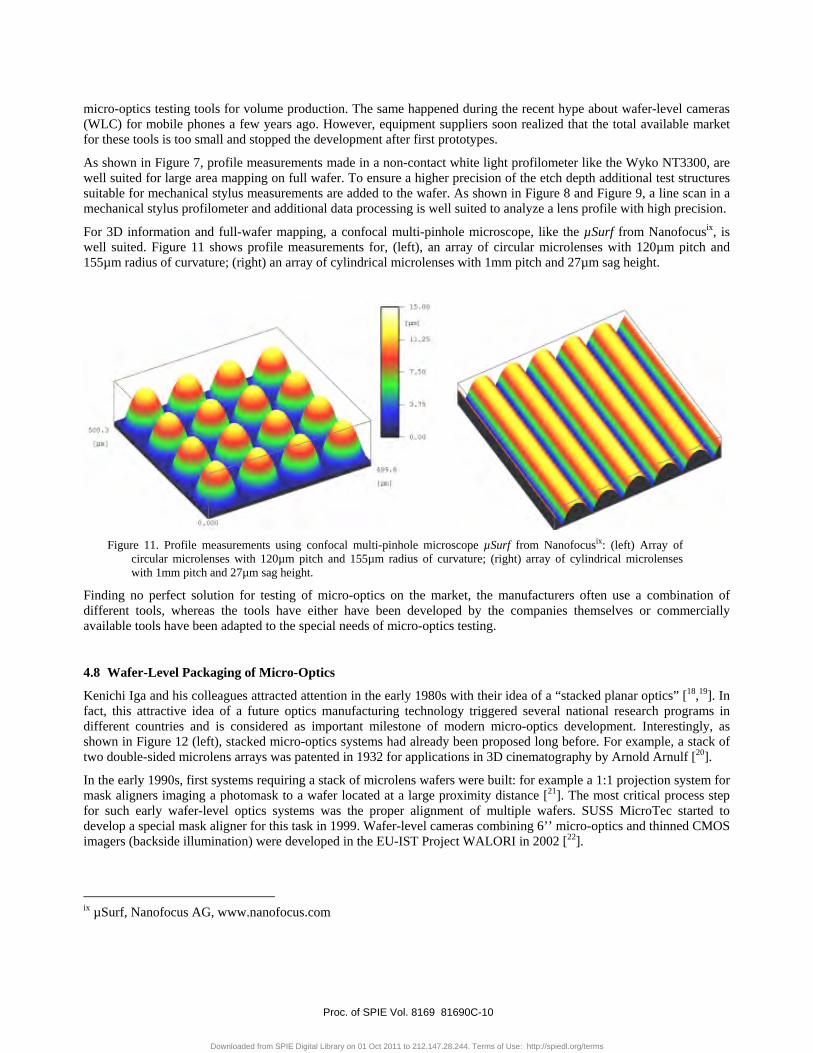
For 3D information and full-wafer mapping, a confocal multi-pinhole microscope, like the µSurf from Nanofocusix, is well suited. Figure 11 shows profile measurements for, (left), an array of circular microlenses with 120µm pitch and 155µm radius of curvature; (right) an array of cylindrical microlenses with 1mm pitch and 27µm sag height.
Figure 11. Profile measurements using confocal multi-pinhole microscope µSurf from Nanofocusix: (left) Array of
circular microlenses with 120µm pitch and 155µm radius of curvature; (right) array of cylindrical microlenses with 1mm pitch and 27µm sag height.
Finding no perfect solution for testing of micro-optics on the market, the manufacturers often use a combination of different tools, whereas the tools have either have been developed by the companies themselves or commercially available tools have been adapted to the special needs of micro-optics testing.
4.8 Wafer-Level Packaging of Micro-Optics
Kenichi Iga and his colleagues attracted attention in the early 1980s with their idea of a “stacked planar optics” [18,19]. In fact, this attractive idea of a future optics manufacturing technology triggered several national research programs in different countries and is considered as important milestone of modern micro-optics development. Interestingly, as shown in Figure 12 (left), stacked micro-optics systems had already been proposed long before. For example, a stack of two double-sided microlens arrays was patented in 1932 for applications in 3D cinematography by Arnold Arnulf [20].
In the early 1990s, first systems requiring a stack of microlens wafers were built: for example a 1:1 projection system for mask aligners imaging a photomask to a wafer located at a large proximity distance [21]. The most critical process step for such early wafer-level optics systems was the proper alignment of multiple wafers. SUSS MicroTec started to develop a special mask aligner for this task in 1999. Wafer-level cameras combining 6’’ micro-optics and thinned CMOS imagers (backside illumination) were developed in the EU-IST Project WALORI in 2002 [22].
ix µSurf, Nanofocus AG, www.nanofocus.com
Proc. of SPIE Vol. 8169 81690C-10
Downloaded from SPIE Digital Library on 01 Oct 2011 to 212.147.28.244. Terms of Use: http://spiedl.org/terms

Wafer-level camera (WLC) for low-cost applications, like mobile phone cameras and disposable endoscopes, has gained much popularity recently. For low-cost systems the micro-optical components are usually fabricated by microlens imprint lithography [23]. Microlens imprint lithography uses soft or hard stamps to imprint microlens arrays in polymer on full wafer level. The microlens wafers and CMOS-wafer are then mounted by wafer-level packaging (WLP). Other imaging applications are ultra-flat multi-pupil camera systems, where the image from multiple micro-cameras is superpose optically or electronically [24,25].
Figure 12. (left) Stack of double-sided microlens arrays as patended by Arnold Arnulf in 1932, (center) a stack of four
100mm microlens wafers serving as 1:1 imaging system for microlens projection lithography, (right) wafer-level camera (NanEye 2B sensor, AWAIBA) serving for disposable endoscopesx.
The equipment supplier SUSS MicroTec now provides two mask aligners, the MA/BA8 Gen3 and the MA200 Compact, especially adapted for wafer-level optics and packaging. The MA/BA8 Gen3 provides optimized thick resist lithography, microlens imprint lithography (SMILE), stamp making tools, UV Bonding and Wafer-Level Packaging (WLP) at ±0.25µm alignment accuracy. The MA200 Compact is a modification of the standard production mask aligner with special capabilities for WLC and WLP. Certainly the availability of dedicated equipment will help much to further commercialize wafer-level optics successfully.
4.9 Conclusion and Outlook
Wafer-level manufacturing is a mature technology today. Equipment, processes and standards from semiconductor industry have been used to establish reliable and repeatable manufacturing processes to provide high-quality micro-optical components for many applications. However, micro-optics remains to be a niche product with a low number of wafers per hour. The motivation for using wafer-level technology is typically not the high-throughput capacity, but quality and compatibility with CMOS, MEMS and other wafer technology. Thus a move from the current 150mm or 200mm to 300mm technology is not attractive for micro-optics manufacturing.
The important role of wafer-level micro-optics is based on different motivations: miniaturization, high functionality and packaging aspects. Especially the recent trends in semiconductor industry, like thin wafer handling (TWH), 3D chip integration (3D-IC) and through-silicon via (TSV), sub-wavelength metal-gratings for color-filtering in CMOS technology, etc. will have significant impact on the prospering micro-optics industry in the future. Typically the costs of a micro-optical component itself are smaller than the costs for system integration and alignment. Thus, the key to future success will be handling, packaging and system integration. Strategies from semiconductor and MEMS industry will be adapted to wafer-level micro-optics.
x Photograph courtesy of AWAIBA, www. awaiba.com
Proc. of SPIE Vol. 8169 81690C-11
Downloaded from SPIE Digital Library on 01 Oct 2011 to 212.147.28.244. Terms of Use: http://spiedl.org/terms

REFERENCES
[1] Lippmann, G., “Photographies des couleurs”, Comptes rendus de l’Académie des Sciences de Paris, pp. 112-114, 1891. [2] Gabor, D., “A new microscopic principle”, Nature 161, pp. 777-778, 1948. [3] Lippmann, G., “Epreuves réversibles. Photographies intégrales“, Comptes rendus de l’Académie des Sciences de Paris, 146 (9), pp. 446-451, 1908. [4] US Patent 1128979, Hess, W. R., “Stereoscopic picture”, filed June 1, 1912. [5] US Patent 1762932, Mihalyi, J, “Projection system for color pictures”, filed May 11, 1927. [6] US Patent 3025589, Hoerni, J. A., “Method of manufacturing semiconductor devices”, filed May 1, 1959. [7] US Patent 4155627, Gale, M. T., Lehmann, H. W., Widmer, R. W.,“Color diffractive subtractive filter master recording comprising a plurality of superposed two-level relief patterns on the surface of a substrate”, filed December 21, 1977. [8] Brown, B. R., Lohmann A. W., “Complex spatial filtering with binary masks”, Appl. Opt. 5, pp. 967ff, 1966. [9] US Patent 3733258, Hanak, J. J., Russell, J. P., “Sputter-etching technique for recording holograms or other fine-detail relief patterns in hard durable materials”, filed in February 1971. [10] US Patent 4689291, Popovic, Z. D., Sprague, R. A., Connell, G. A. N., “Pedestal-type microlens fabrication process”, filed August 30, 1985. [11] Voelkel R., Vogler, U., Bich, A., Pernet, P., Weible, K. J., Hornung, M., Zoberbier, R., Cullmann, E., Stuerzebecher, L., Harzendorf, T., and Zeitner, U. D., "Advanced mask aligner lithography: new illumination system," Opt. Express 18, 20968-20978 (2010). [12] Nussbaum, Ph., Voelkel, R., Herzig, H. P., Eisner, M., Haselbeck, S., „Design, fabrication and testing of microlens arrays for sensors and microsystems“, Pure Appl. Opt. 6, 617 – 636 (1997). [13] Harzendorf, T., Stuerzebecher, L., Vogler, U., Zeitner, U. D., Voelkel, R., "Half-tone proximity lithography", Proc. SPIE 7716, 77160Y (2010), http://dx.doi.org/10.1117/12.854307. [14] Stuerzebecher, L., Harzendorf, T., Vogler, U., Zeitner, U. D., Voelkel, R., "Advanced mask aligner lithography: fabrication of periodic patterns using pinhole array mask and Talbot effect," Opt. Express 18, 19485-19494 (2010). [15] Schwider, J. , Falkenstörfer, O., “Twyman-Green interferometer for testing microspheres”, Opt. Eng. 34, p.2972-2975 (1995). [16] Dresel, T., Horstmann, A., Otto, A., Schwider, J., “UV interferometry for microstructure measurements“, Pure Appl. Opt. 1, p.241 (1992). [17] Sickinger,, H., Schwider, J., Manzke, B., “Fiber based Mach-Zehnder interferometer for measuring wave aberrations of microlenses”, Optik (Germany) , 110 , p.239 (1999 ). [18] Iga, K., Oikawa, M., Misawa, S., Banno, J., Kokubun, Y., “Stacked planar optics: an application of the planar microlens”, Appl. Opt., Vol. 21, No. 19 (1982). [19] Iga, K., Y Kokubun, Y., Oikawa, M., “Fundamentals of Microoptics: Distributed-Index, Microlens, and Stacked Planar Optics”, Academic Press Inc, ISBN-10: 0123703603 (1984). [20] US Patent 2,018,592, Arnulf, A., “Cinematography in relief”, filed December 5, 1932. [21] Voelkel, R., Herzig, H. P., Nussbaum, Ph., Singer, W., Weible, K. J., Daendliker, R., Hugle, W. B., “Microlens lithography: a new fabrication method for very large displays”, Asia Display'95, pp. 713-716, (1995). [22] EU-IST-2001-35366, Project WALORI, WAfer Level Optic solution foR compact CMOS Imager (2002-2005). [23] Voelkel, R., Duparre, J., Wippermann, F., Dannberg, P., Braeuer, A., Zoberbier, R., Hansen, S., Suess, R., „Technology trends of microlens imprint lithography and wafer level cameras (WLC)”, 14th Micro-optics conference (MOC‚ 08), 25.–27.9.2008, Brussels, Belgium Techn. Dig. p. 312–315 (2008). [24] Voelkel, R., Wallstab, S., „Flachbauendes Bilderfassungssystem“ Patent DE 19917890 A1 (1999). [25] Duparré, J., Dannberg, P., Schreiber, P., Voelkel, R., Braeuer, A., „Bilderfassungssystem und dessen Verwendung“, Deutsche Patentanmeldung 10 2001 003 013.8(2004).
Proc. of SPIE Vol. 8169 81690C-12
Downloaded from SPIE Digital Library on 01 Oct 2011 to 212.147.28.244. Terms of Use: http://spiedl.org/terms