Embed Size (px)
Citation preview

W23.004
Synthesis and Assembly of Nickel Nanoparticles
by Electrodeposition onConductive Polymer Electrodes
N. F. Heinig, N. Kharbanda, X.J. Zhou, K.T. LeungDept. of Chemistry, University of Waterloo, Waterloo, Canada
G. A. ScholzDept. of Physics, University of Waterloo, Waterloo, Canada
Acknowledgements: NSERC, CFI and OIT.

Motivation
• Electron-conducting polymers (ECP) are quasi-metallic materials long proposed as a good conductive substrate to support dispersed nanoparticles for catalytic and other applications.
• Electrochemical deposition of these polymers can produce films of well-controlled purity, thickness and morphology. Applications include anti-static coatings, batteries, sensors and more recently, LEDs and other electronic devices.
• Uniformly sized, uniformly dispersed nickel nanoparticles on ECP substrates have potential for unique magnetic, electrical and chemical properties.

Background
Electrical conductivity is introduced by doping the polymer. The delocalized charge then moves along the carbon chain backbone.
The first ECP, polyacetylene, was discovered in 1977.
Commonly studied ECP include polypyrrole (PPy), polyaniline (PAni), and polythiophene (PT).
PPy is easily oxidized (p-doped) , which is usually done simultaneously with electrodeposition.
200 nm
SE 5kV
200 nm
RBS 5kV
LEO 1530 FE-SEM

Procedure:
Silicon is sputter coated with gold.
Conductive polypyrrole films are grown from aqueous pyrrole solution: 0.05M pyrrole, 0.1M NaClO4
Pyrolle is deposited and polymerized galvanostatically (constant current). By monitoring the total charge transfer, the polymer film thickness can be accurately determined.ref. S. Sadki et al., Chem. Soc. Rev. 2000, 29, 283-293.
Nickel particles are grown from Ni solution: 1 µM H2SO4, 0.01 M H3BO3, 0.01 M NiSO4·6H2O
Ni is deposited on the composite films potentiostatically. Since hydrogen is evolved when nickel is deposited, the amount of nickel deposited cannot be determined from the total charge transferred. ref. A. Lachenwitzer, O.M. Magnussen, J. Phys.Chem. B 2000, 104, 7424.
M.P. Zach, R.M. Penner, Adv. Mat. 2000, 12, 878-883.
Parameters studied: Gold thickness, Ppy thickness, Ni potential, Total charge transfer (Ni ).

NiPPyAuSi
Depending on how the gold was deposited,The PPY deposition would occur as a 1-step or 2-step process:
Larger Ni particle growth
Nanoparticle Ni growth
Baking the Si before gold deposition leads to 2-step PPy growth.
For gold thicknesses of 80-100 nm, the highest density of nickel particles were found.
For 100 nm Au, and Ni deposition of 1.4V and 2.6mC:90-110 nm PPy: even distribution of nanoparticles.
For 100 nm Au, 75 or 100 nm PPy, and total charge is 2.6 or 1.9 mC:-1.3 to -1.6 V: uniformly sized and shaped nanoparticles.
Small region in parameter space fornickel nanoparticle growth.

PPY deposition conditions control nickel morphology.
2 um
200 nm
200 nm
C
A

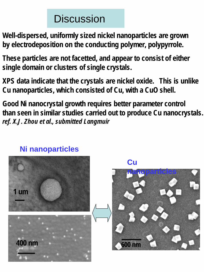
Charge transfer (total deposition time) of the Ni is varied.
100 nm Au, 100 nm PPy, Nickel voltage = -1.4 V.
The particle size appears roughly constant, but the number density of Ni particles increases with total charge deposited.
050
100150200250300350
1.3 1.9 2.6 3.2
200 nm
1.3 mC
2.6 mC 3.2 mC
200 nm
200 nm
Number density →
Size↓

Optimization of growth conditions leads to well-dispersed, uniformly-sized nickel nanoparticles.
200 nm
FE-SEM micrograph: 5 kV, SE detector- sample 23-5
200 nm
TEM micrograph: 200 kV – sample 23-5

TEM images shows rounded particles, without facetting.
11 nm
Diffraction and dark field images indicate the nanoparticles can consist of clusters of crystallites.
22 nm
Bright field Dark Field 1 Dark Field 2

X-ray Photoelectron Spectroscopy Results (Sample 23-6)
0
2
4
6
8
10
12
14
16
18
0 100 200 300 400 500 600 700 800 900 1000 1100
Binding Energy (eV)
Survey
0
2
4
6
8
10
12
14
16
18
850 860 870 880
Binding Energy (eV)
Ni2p
NiNiO
Ni2O3
Increasing Sputtering Time
Nickel particles consist of NiO, with a Ni2O3 outer shell.
C
N O
Data from a VG-ESCALab 250, with energy resolution of 0.4-0.5 eV FWHM,and step size of 0.1 eV.
DiscussionWell-dispersed, uniformly sized nickel nanoparticles are grown by electrodeposition on the conducting polymer, polypyrrole.
These particles are not facetted, and appear to consist of either single domain or clusters of single crystals.
XPS data indicate that the crystals are nickel oxide. This is unlike Cu nanoparticles, which consisted of Cu, with a CuO shell.
Good Ni nanocrystal growth requires better parameter controlthan seen in similar studies carried out to produce Cu nanocrystals. ref. X.J. Zhou et al., submitted Langmuir
Ni nanoparticles
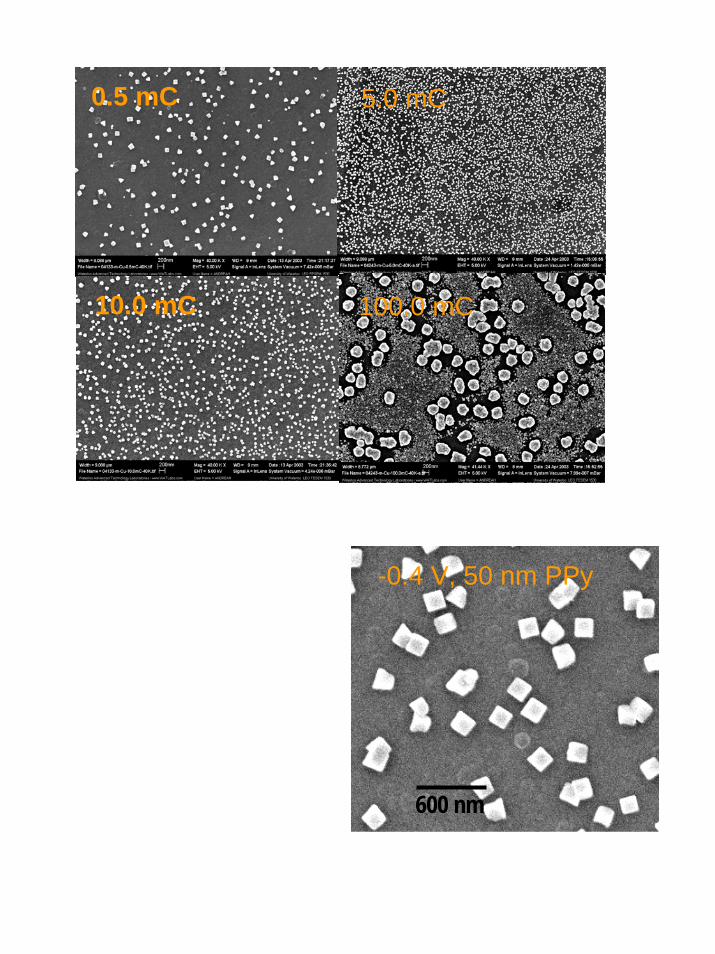
Cu nanoparticles
600 nm
1 um
400 nm

0.5 mC 5.0 mC
10.0 mC 100.0 mC
-0.4 V, 50 nm PPy
600 nm

Sample 23-5: small Nickel particles

XPS Data for the Large Nickel Clusters (Sample 7-5)
Ni
0
2
4
6
8
10
12
14
16
18
0 100 200 300 400 500 600 700 800 900 1000 1100
Binding Energy (eV)
Survey2000
3000
4000
5000
6000
850 860 870 880
Cou
nts
/ s
Binding Energy (eV)
Ni2p
Increasing Sputtering Time
NiO

Outline• Motivation: • Background• Procedure• Results• Discussion