Embed Size (px)
Citation preview

W-Band Low-Profile Monopulse Slot Array Antenna Based on GapWaveguide Corporate-Feed Network
Downloaded from: https://research.chalmers.se, 2020-03-21 00:48 UTC
Citation for the original published paper (version of record):Vosoogh, A., Haddadi, A., Uz Zaman, A. et al (2018)W-Band Low-Profile Monopulse Slot Array Antenna Based on Gap Waveguide Corporate-Feed NetworkIEEE Transactions on Antennas and Propagation, 66(12): 6997-7009http://dx.doi.org/10.1109/TAP.2018.2874427
N.B. When citing this work, cite the original published paper.
©2018 IEEE. Personal use of this material is permitted.However, permission to reprint/republish this material for advertising or promotional purposesor for creating new collective works for resale or redistribution to servers or lists, or toreuse any copyrighted component of this work in other works must be obtained fromthe IEEE.
This document was downloaded from http://research.chalmers.se, where it is available in accordance with the IEEE PSPBOperations Manual, amended 19 Nov. 2010, Sec, 8.1.9. (http://www.ieee.org/documents/opsmanual.pdf).
(article starts on next page)

1
W-Band Low-Profile Monopulse Slot Array AntennaBased on Gap Waveguide Corporate-Feed NetworkAbbas Vosoogh, Abolfazl Haddadi, Ashraf Uz Zaman, Jian Yang, Herbert Zirath, Fellow, IEEE, and Ahmed A.
Kishk, Fellow, IEEE
Abstract—This paper presents a gap waveguide based compactmonopulse array antenna, which is formed with four unconnectedlayers, for millimeter-wave tracking applications at W-band(85–105 GHz). Recently developed gap waveguide technologyremoves the need for galvanic contact among metallic layers ofwaveguide structures, and thereby, makes the proposed antennasuitable for easy and low-cost manufacturing. In this context, alow-loss planar Magic-Tee is designed to be used in a monopulsecomparator network consisting of two vertically stacked layers.The gap waveguide planar monopulse comparator network isintegrated with a high-efficiency 16×16 corporate-fed slot arrayantenna. The measured results of the comparator network showthe amplitude and phase imbalance values to be less than 0.5 dBand 2◦, respectively, over the frequency band of interest. Thefabricated monopulse array antenna shows relative impedancebandwidths of 21% with input reflection coefficients better than−10 dB for the sum and difference ports. The null in thedifference radiation pattern is measured to be 38 dB below thepeak of the sum radiation pattern at 94 GHz. The measured gainis about 30 dBi for the same frequency. The low-loss performanceof the comparator network and the feed-network of the proposedarray, together with the simple and easy manufacturing andmechanical assembly, makes it an excellent candidate for W-bandcompact direction-finding systems.
Index Terms—Monopulse antenna, high-efficiency, integration,millimeter-wave, gap waveguide, slot array antenna.
I. INTRODUCTION
M Illimeter-wave technologies have been under investi-gation and development in recent years, in response to
the demanding needs for extremely high data rate transmissionand highly integrated low-cost and low-power wireless devicesfor different applications, such as high-definition video, au-tomotive radars, and high-resolution imaging [1]. The hugeavailable bandwidth in the millimeter-wave frequency band(30–300 GHz) represents a great potential in terms of capacityand flexibility. For example, E-band (60–90 GHz) and W-band(75–110 GHz) are attractive for multi-Gbps wireless links andradar systems, due to their low atmospheric absorption, shortwavelength, and available bandwidth [2].
Direction finding (DF) techniques are necessary for differentmillimeter-wave applications, such as finding the position
This work is financially supported by the European Research Council (ERC)under the 7th Framework Program ERC grant number 321125.
A. Vosoogh, A. Uz Zaman, and J. Yang are with the Electrical EngineeringDepartment at Chalmers University of Technology, Gothenburg, Sweden (e-mails: [email protected]).
A. Haddadi is with Gapwaves AB, Gothenburg, Sweden.H. Zirath is with the Department of Microtechnology and Nanoscience,
Chalmers University of Technology, Gothenburg.A. A. Kishk is with the Electrical and Computer Engineering Department,
Concordia University, Montreal, Canada.
of objects in radar systems, determining the line-of-sightdirection in point-to-point wireless links, and detecting the lo-cation of unlicensed or undesired radiation sources in securityapplications. As a technique to measure the direction of arrivalof radiation or backscattered wave, monopulse technique hasmany potential applications, not only in direction-finding, butalso in communications, radio astronomy, and sonar [3].
Millimeter-wave monopulse radars are attractive for high-resolution tracking applications. They can provide a narrowbeamwidth for high angular accuracy with a relatively smallaperture size [4]. To reach a narrow beamwidth for high-gain monopulse tracking radars, reflector antennas are typicalcandidates, due to their simple design and good performance[5], [6]. However, reflector antennas are bulky due to theirthree-dimensional structure. Moreover, in millimeter-wave fre-quencies, the requirements for high surface accuracy (betterthan λ/20) for reflectors become more demanding (better than150 µm at 100 GHz) [7], [8]. Microstrip reflectarray antennascan be a low-profile and low-cost alternative to reflectorantennas, and they have been used for W-band monopulseradar systems [9]. However, complicated design, needs forlow-loss substrates, and narrow bandwidth are some of thedrawbacks of the substrate based reflectarray antennas.
Planar array antennas can provide high-gain performancetogether with compact and low-profile structure for monopulseapplications. The operating bandwidth of an array antenna ismainly limited by its feed-network. Corporate-feeding, whichis frequency independent compared to the series feeding,enables a wide bandwidth by in-phase excitation of all radi-ating elements [10]. Different transmission line technologiescan be used to realize planar array antennas for monopulseapplications. Hollow waveguide feeding networks introduceno dielectric loss, low conductive loss, and capability tohandle high power. The critical challenge of multi-layer hollowwaveguide arrays, especially at millimeter-wave frequencies,is achieving good electrical contact among the building blocksof the complicated waveguide structure. Good electrical andgalvanic contact can be achieved by using elaborate manufac-turing methods, such as diffusion bonding of many thin metallayers [11], which increases fabrication cost and manufactur-ing complexity [12]. Microstrip lines and Substrate IntegratedWaveguides (SIW) are other types of transmission lines, whichcan be used for a wideband planar array for monopulseapplications [13]–[15]. Antennas implemented using thesesubstrate-based transmission lines suffer from low efficiencydue to dielectric loss and field leakage in the substrate. Thelosses can be partly reduced by using low loss dielectrics.

2
The gap waveguide technology, firstly proposed in [16] and[17], is a guiding structure that can achieve low-loss perfor-mance, manufacturing flexibility, and cost effectiveness as wellas no need for galvanic contact among the different buildingblocks of the waveguide structure. In gap waveguide tech-nology the direction of propagation of the wave is controlledby using a guiding structure such as ridge [17] or invertedmicrostrip line [18] in parallel-plate waveguide configuration.A periodic electromagnetic bandgap (EBG) structure, i.e. a pintexture, around the guiding structure eliminates any possibleleakage and higher order modes. The EBG structure also canbe used to form the guiding structure, for example in groovegap waveguide [19]. Different millimeter-wave devices such asantennas [12], [20]–[25], filters [26]–[32], and diplexers [33]–[36] have been reported with good performance based on thisnew technology. Moreover, different fabrication techniquessuch as Computer Numerical Control (CNC) machining [20],[37], die-sink Electric Discharge Machining (EDM) [22],Direct Metal Laser Sintering (DMLS) 3D printing [38], [39],and printed circuit board technology (PCB) [24], [25], suggestflexible manufacturing methods with affordable cost.
In this paper, we present the integration of a wide-band planar monopulse comparator network with a high-gain corporate-fed slot array antenna based on gap waveguidetechnology. The proposed module has a novel and flexible ar-chitecture with high-efficiency and wide impedance bandwidth(85–105 GHz). The proposed monopulse antenna is formedby four unconnected layers. There is no need for electricaland galvanic contact among the layers, and this makes theantenna easier to manufacture and assemble mechanically.All these features make the proposed antenna a suitablecandidate for 2-D (E- and H-planes) tracking applicationsat W-band. In Section II the design of the Magic-Tee usinggap waveguide transmission line is presented. Designing thecomparator network based on the presented Magic-Tee isanother part of this section. The design of the radiating unitcell and the integration of the monopulse comparator networkwith the feed-network of a 16×16 array antenna is presentedin Section III. Experimental results and a comparison withseveral published works on different technologies are given inSection IV. Finally, Section V gives some concluding remarks.
II. DESIGN OF THE MONOPULSE COMPARATOR NETWORK
The key component of any monopulse antenna system isthe comparator network. It enables the system to constructthe sum and differences patterns. Based on the sum anddifference signals, one can find the direction of the target orthe electromagnetic emission. Magic-Tees consist of E- and H-plane T-junctions in 3-D form can be used to construct sumand difference signals in monopulse systems based on hollowwaveguides. Fabrication of the 3-D waveguide structure is achallenging task due to the need for perfect electrical contactbetween the junctions, especially at high frequency.
In this section, we present the design of a planar monopulsecomparator network based on gap waveguide technology.In the proposed architecture a comparator network in threedistinct layers is formed and stacked on top of each otherwithout any electrical contact requirements.
couplingaperture
Port 3
Port 4
Stepl1s ws
l2s
h1s
hs
Port 1 (S)
Port 2 (D)
pintexture
(a)
wq
lqwr
lt
Port 4Port 3
coupling aperturePort 1 (S)
a1p1
wcm
lcmwG
lb
a2p2
Port 2(D)
step
(b) (c)Fig. 1. Proposed planar gap waveguide Magic-Tee. (a) Exploded view. (b)Top view of bottom layer. (c) Top view of the middle layer. (a1 = 0.65 mm,p1 = 1.3 mm, l1s = 0.5 mm, l2s = 0.73 mm, h1s = 0.23 mm, hs = 0.49 mm,ws = 1.2 mm, wr = 0.65 mm, wq = 0.88 mm,a2 = 0.52 mm, d2 = 0.55 mm,lt = 1.1 mm, lq = 1 mm, wG = 2.5 mm, lcm = 2 mm, wcm = 0.42 mm,lb = 1.24 mm).
A. Gap waveguide Magic-Tee design
The exploded view of the proposed wideband Magic-Teeis shown in Fig. 1(a). The planar configuration of the Magic-Tee can be used to realize a low-profile comparator networkwith the capability of easy integration with planar arrayantennas. The electromagnetic coupling mechanism of the gapwaveguide Magic-Tee is similar to the conventional hollowwaveguide Magic-Tee.
The proposed Magic-Tee is implemented in three distinctmetal layers by combination of E- and H-planes 3 dB powerdividers, as shown in Fig. 1(a). The pin texture acts as ahigh impedance surface and prevents electromagnetic wavesto propagate and leak in undesired directions within a specificfrequency band (stopband). Based on gap waveguide concept,all the metal layers are separated by a small gap, and thereis no requirement for a metallic contact among the layers,in Fig. 1. Furthermore, electromagnetic waves are guidedby forming a groove by using pins on the middle layerand ridges on the bottom layer. All the possible leakagesare eliminated by using periodic pins, as an electromagneticbandgap structure, around the guiding structures.

3
0 20 40 60 80 100 120 140 1600
500
1,000
1,500
2,000
2,500
Stopband=40–150 GHz
Frequency (GHz)
β(rad
/m)
Mode 1 Mode 2
d1
g1
a1
p1
Fig. 2. Dispersion diagram for the infinite periodic pin unit cell.(d1 = 0.78 mm, a1 = 0.65 mm, g1 = 0.07 mm, and p1 = 1.3 mm)
0 20 40 60 80 100 120 140 160 180 200 2200
1,000
2,000
3,000
Quasi-
TEMmod
e
Single-mode band
Frequency (GHz)
β(r
ad/m
)
Mode 1 Mode 2Mode 3 Mode 4Mode 5 Mode 6Mode 7 Mode 8Mode 9 Mode 10
a2
p2g2
drwr
d2
Fig. 3. Dispersion diagram for the infinite ridge and periodic pin unit cell(d2 = 0.55 mm, a2 = 0.52 mm, g2 = 0.03 mm, p2 = 0.92 mm, dr = 0.38 mm,wr = 0.65 mm).
By exciting the Port 3 and Port 4, the sum and differencesignals will be constructed in the Port 1 (Σ) and Port 2 (∆),respectively. A ridge gap waveguide H-plane T-junction, onthe bottom layer in Fig. 1(b), is used for the sum port. Acoupling slot on the middle layer forms an E-plane T-junctionto subtract the signal at the Port 3 from the signal at the Port 4and delivers the difference signal to the Port 2. The E-planeT-junction on the middle layer is implemented in groove gapwaveguide. The reason we have used ridge gap waveguideas the transmission line on the bottom layer is due to thefact that the designed Magic-Tee will be used to implementa comparator network, which itself will integrate with feed-network of an array antenna afterward. The feeding networkof the array antenna is in ridge gap waveguide, due to thelimited space for corporate feeding.
In the bottom layer, a post with a base length of ltand a trapezoidal cut in the ridge T-junction are optimizedto have wideband impedance matching for the Σ port, asshown in Fig. 1(b). The coupling slot on the middle layerin combination with a step on the top layer acts as an E-plane T-junction for the difference port. The proposed Magic-Tee is optimized by using CST Microwave Studio to havelow reflection coefficients at all ports, good isolation betweenthe sum and difference ports, and low amplitude and phase
86 88 90 92 94 96 98 100 102 104−60
−40
−20
0
SΣ
S∆
S3,∆, S4,∆, S3,Σ , S4,Σ
S∆,Σ, SΣ,∆
Frequency (GHz)
Spa
ram
eter
s(d
B)
Fig. 4. Simulated performance of the proposed gap waveguide Magic-Tee.
85 90 95 100 105−0.5
−0.25
0
0.25
0.5
Frequency (GHz)A
mpl
itud
e(d
B)
SdB4,Σ − SdB
3,Σ
SdB4,∆ − SdB
3,∆
85 90 95 100 105−1
−0.5
0
0.5
1
Frequency (GHz)
Pha
se(d
eg)
85 90 95 100 105179
179.5
180
180.5
181deg(S4,Σ)−deg(S3,Σ)deg(S4,∆)−deg(S3,∆)
(a) (b)Fig. 5. Simulated amplitude and phase error at the outputs of the Magic-Tee.(a) Amplitude error. (b) Phase error.
imbalance values at the output ports (Port 3 and Port 4).
The dispersion diagram of the periodic pin unit cell ofthe pin texture on the middle layer (Fig. 1(c)) is illustratedin Fig. 2. The pin texture with the given values provides astopband over the frequency band 40–150 GHz, covering thefrequency band of interest. Fig. 2 shows that, even with thepresence of a small gap between the pin and the upper plate,there is no propagating mode within the stopband. The pintexture on the bottom layer has a different size from those onthe middle layer. On the bottom layer, ridge gap waveguide andsmaller pins are used to realize a compact comparator network.Fig. 3 shows the dispersion diagram of the unit cell of a ridgeand pins, similar to the one on the bottom layer of the designedMagic-Tee (Fig. 1(b)). A single quasi-TEM mode propagationis achieved over the frequency band of 65–160 GHz.
Fig. 4 shows the simulated performance of the designedMagic-Tee. The sum (Σ) and difference (∆) ports have re-flection coefficients better than −28 dB and −20 dB, respec-tively, over the frequency band 85–100 GHz. Furthermore, theisolation between the Σ and ∆ ports is better than 49 dB.The output ports (Port 3 and Port 4) have about 0.05 dBamplitude imbalance for both the sum and difference inputports. As shown in Fig. 5, the simulated phase imbalance isfound to be better than 0.5◦. The proposed Magic-Tee shows awide impedance bandwidth, where the operational bandwidthis mainly limited by the bandwidth of the difference port andthe E-plane T-junction.

4
Port SPort DE
Port DH
WR-10
Transitionstep
bottom layer
top layer
middle layer
Fig. 6. Configuration of the proposed monopulse comparator network.
Port S
Port 1
Port 3 Port 4
Port 2
(a) (b)Fig. 7. Simulated E-field for the sum port at 94 GHz.
B. Monopulse comparator network design
A monopulse comparator network is designed by usingthe proposed gap waveguide Magic-Tee. Fig. 6 shows theconfiguration of the comparator network. Three input ports(Ports Σ, ∆E , and ∆H ) on the top layer deliver sum, H-plane,and E-plane difference signals, respectively. The energy fromthe sum port on the top layer is coupled to the ridge feed-network on the bottom layer via a right-angle transition. Asthe summation happens on the bottom layer and the sum port isplaced on the top layer, a pin texture is placed around the sumwaveguide on the middle layer to prevent any field leakagesince there is a gap between top and middle layers.
The middle and top layers in Fig. 6 will be used in the finalmonopulse array antenna design in Fig. 17 as Layers 3 and4, respectively. The bottom layer of the comparator networkis used to have four ports to simulate 2-D direction findingperformance. Since the designed comparator network is goingto be integrated with the feed-network of the array antenna,the pin and ridge dimensions on the bottom layer are similarto those for the antenna feed-network. Simple E-plane probetransitions, similar to the one in [33] are used at the Ports 1–4to match the quasi-TEM mode of the ridges on the bottomlayer to TE10 of the standard WR-10 waveguides, as shownin Fig. 6.
Fig. 7 illustrates the simulated electric field on the bottomlayer when the Port Σ is excited. In Fig. 7(b), by using two-stage power dividers, the delivered electric fields to the Ports
Port DE
(a) (b)Fig. 8. Simulated E-field for the E-plane difference port at 94 GHz.
Port DH
(a) (b)Fig. 9. Simulated E-field for the H-plane difference port at 94 GHz.
1–4 are equal in phase and amplitude, or
S1,Σ = S2,Σ = S3,Σ = S4,Σ.
In other words, the summation of the signals from the Ports1–4 will appear at the Port Σ. Furthermore, Fig. 7(a) showsthere is no leakage into the middle layer by exciting Port Σdue to the use of pins around the port opening in the middlelayer.
Fig. 8 shows the simulated electric field distribution byexciting the ∆E port. A single Magic-Tee at the center isused in the ∆E channel. It can be seen in Fig. 8(a) that nofield leaks into the Σ and ∆H channels. Furthermore, fieldsat the Ports 1 and 3 are out of phase with those at the Ports2 and 4, with equal amplitudes, or
S1,∆E= −S2,∆E
= S3,∆E= −S4,∆E
.
The H-plane difference channel consists of two Magic-Teesthat are connected via a power divider on the middle layer.The electric field distribution for the wave propagating fromthe ∆H port on the top layer to the middle layer is shownin Fig. 9(a). Some field leakage can be seen between thepins and surrounding internal walls, which does not affectthe performance since there is no strong leakage into theother channels. Two slots on the middle layer couple the waveinto the bottom layer for the H-plane difference channel. InFig. 9(b), all the output Ports 1–4 have equal amplitude without-of-phase fields at Ports 1, 2 and Ports 3, 4, or
S1,∆H= S2,∆H
= −S3,∆H= −S4,∆H
.
5
85 90 95 100 105−30
−25
−20
−15
−10
−5
0
Frequency (GHz)
Am
plit
ude
(dB
)SΣ
S∆E
S∆H
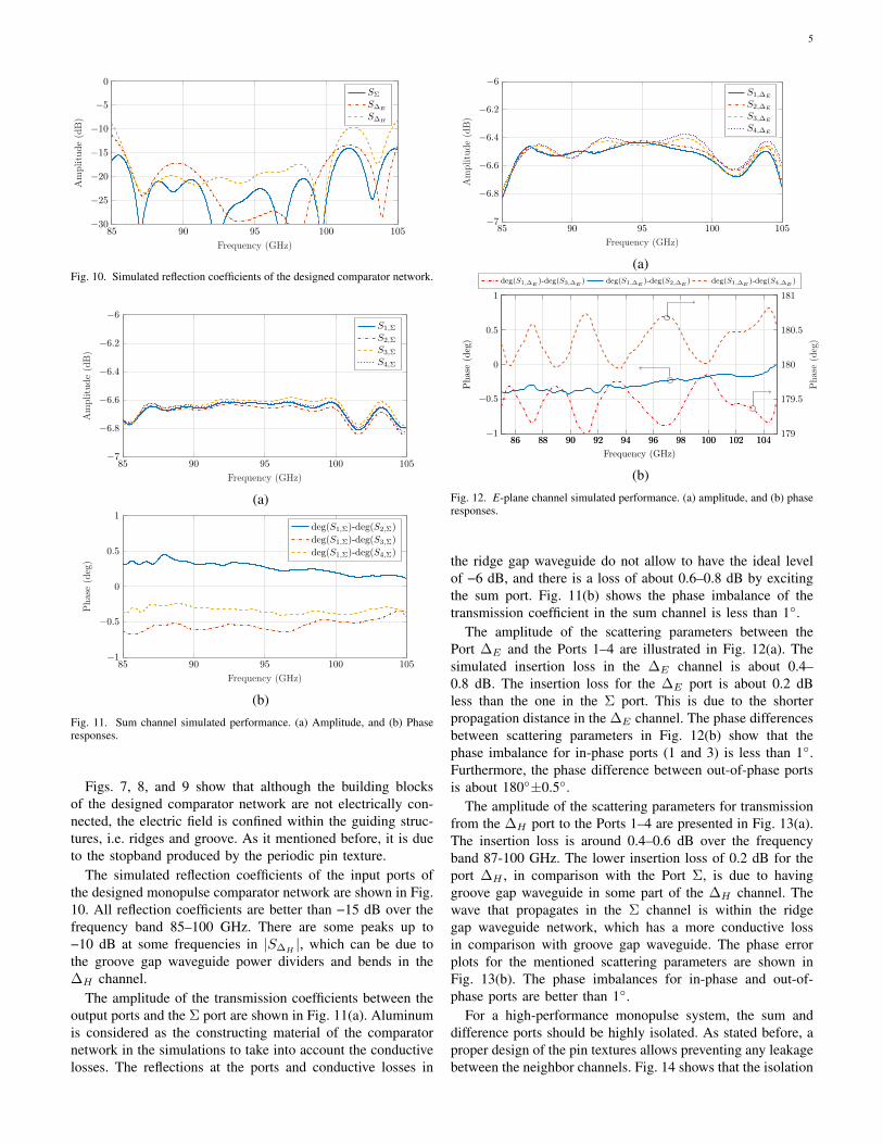
Fig. 10. Simulated reflection coefficients of the designed comparator network.
85 90 95 100 105−7
−6.8
−6.6
−6.4
−6.2
−6
Frequency (GHz)
Am
plit
ude
(dB
)
S1,Σ
S2,Σ
S3,Σ
S4,Σ
(a)
85 90 95 100 105−1
−0.5
0
0.5
1
Frequency (GHz)
Pha
se(d
eg)
deg(S1,Σ)-deg(S2,Σ)deg(S1,Σ)-deg(S3,Σ)deg(S1,Σ)-deg(S4,Σ)
(b)Fig. 11. Sum channel simulated performance. (a) Amplitude, and (b) Phaseresponses.
Figs. 7, 8, and 9 show that although the building blocksof the designed comparator network are not electrically con-nected, the electric field is confined within the guiding struc-tures, i.e. ridges and groove. As it mentioned before, it is dueto the stopband produced by the periodic pin texture.
The simulated reflection coefficients of the input ports ofthe designed monopulse comparator network are shown in Fig.10. All reflection coefficients are better than −15 dB over thefrequency band 85–100 GHz. There are some peaks up to−10 dB at some frequencies in |S∆H
|, which can be due tothe groove gap waveguide power dividers and bends in the∆H channel.
The amplitude of the transmission coefficients between theoutput ports and the Σ port are shown in Fig. 11(a). Aluminumis considered as the constructing material of the comparatornetwork in the simulations to take into account the conductivelosses. The reflections at the ports and conductive losses in
85 90 95 100 105−7
−6.8
−6.6
−6.4
−6.2
−6
Frequency (GHz)
Am
plit
ude
(dB
)
S1,∆E
S2,∆E
S3,∆E
S4,∆E
(a)
86 88 90 92 94 96 98 100 102 104−1
−0.5
0
0.5
1
Frequency (GHz)P
hase
(deg
)
86 88 90 92 94 96 98 100 102 104179
179.5
180
180.5
181
Pha
se(d
eg)
deg(S1,∆E)-deg(S3,∆E
) deg(S1,∆E)-deg(S2,∆E
) deg(S1,∆E)-deg(S4,∆E
)
(b)Fig. 12. E-plane channel simulated performance. (a) amplitude, and (b) phaseresponses.
the ridge gap waveguide do not allow to have the ideal levelof −6 dB, and there is a loss of about 0.6–0.8 dB by excitingthe sum port. Fig. 11(b) shows the phase imbalance of thetransmission coefficient in the sum channel is less than 1◦.
The amplitude of the scattering parameters between thePort ∆E and the Ports 1–4 are illustrated in Fig. 12(a). Thesimulated insertion loss in the ∆E channel is about 0.4–0.8 dB. The insertion loss for the ∆E port is about 0.2 dBless than the one in the Σ port. This is due to the shorterpropagation distance in the ∆E channel. The phase differencesbetween scattering parameters in Fig. 12(b) show that thephase imbalance for in-phase ports (1 and 3) is less than 1◦.Furthermore, the phase difference between out-of-phase portsis about 180◦±0.5◦.
The amplitude of the scattering parameters for transmissionfrom the ∆H port to the Ports 1–4 are presented in Fig. 13(a).The insertion loss is around 0.4–0.6 dB over the frequencyband 87-100 GHz. The lower insertion loss of 0.2 dB for theport ∆H , in comparison with the Port Σ, is due to havinggroove gap waveguide in some part of the ∆H channel. Thewave that propagates in the Σ channel is within the ridgegap waveguide network, which has a more conductive lossin comparison with groove gap waveguide. The phase errorplots for the mentioned scattering parameters are shown inFig. 13(b). The phase imbalances for in-phase and out-of-phase ports are better than 1◦.
For a high-performance monopulse system, the sum anddifference ports should be highly isolated. As stated before, aproper design of the pin textures allows preventing any leakagebetween the neighbor channels. Fig. 14 shows that the isolation

6
85 90 95 100 105−7
−6.8
−6.6
−6.4
−6.2
−6
Frequency (GHz)
Am
plit
ude
(dB
)S1,∆H
S2,∆H
S3,∆H
S4,∆H
(a)
86 88 90 92 94 96 98 100 102 104−1.5
−1
−0.5
0
0.5
1
1.5
Frequency (GHz)
Pha
se(d
eg)
86 88 90 92 94 96 98 100 102 104178.5
179
179.5
180
180.5
181
181.5
Pha
se(d
eg)
deg(S1,∆H)-deg(S2,∆H
)deg(S1,∆H
)-deg(S3,∆H)
deg(S1,∆H)-deg(S4,∆H
)
(b)Fig. 13. H-plane channel simulated performance. (a) Amplitude, and (b)Phase responses.
85 90 95 100 105−80
−60
−40
−20
0
Frequency (GHz)
Am
plit
ude
(dB
)
S∆E ,Σ
S∆H ,Σ
S∆E ,∆H
Fig. 14. Simulated isolation between the input ports of the designedcomparator network.
between the sum port and each of the difference ports (S∆E ,Σ
and S∆H ,Σ) are better than 50 dB. Moreover, isolation betterthan 60 dB has been achieved between the two difference ports(S∆E ,∆H
).
III. PLANAR MONOPULSE ARRAY ANTENNA DESIGN
A 4×4 cavity-backed slot array, as shown in Fig. 15, isdesigned as subarray for the antenna array. The subarrayconsists of three unconnected layers, i.e., radiating layer,cavity layer, and feeding layer. Each radiating slot is non-concentrically surrounded by a rectangular cavity on the top,with the height Hsu, to reduce slot-to-slot coupling. The slotsare fed by rectangular cavities to provide a uniform magneticfield on each radiating slot in the unit cell. The radiating slotsare rotated by 10◦ in order to achieve low side-lobe levelson the E-, and H-planes. The slot rotation can separate theprincipal radiation planes from the array lattice planes, e.g. x-z
dr
Radiating layer
Feeding layer
Couplingaperture
Cavity layer
Ridge line
wc lcu
wr2
wcu
lsu
wsu
Hsu
Slotslc
Fig. 15. Gap Waveguide 4 × 4 cavity-backed slot subarray (lsu = 1.8 mm,wsu = 1 mm, Hsu = 0.76 mm, wc = 4.5 mm, lc = 3.9 mm, lcu = 1.75 mm,wcu = 0.73 mm, wr2 = 0.44 mm).
80 85 90 95 100 105 110−25
−20
−15
−10
−5
0
Frequency (GHz)
S11
(dB
)
Fig. 16. Simulated reflection coefficient of 4 × 4 slots subarray in infinitearray environment.
and y-z planes, as explained in [12]. Each excited cavity is fedvia a coupling slot from a ridge gap waveguide feed network.The unit cell could have been chosen to be 2×2 slots overone feeding cavity without any power divider on the bottomfeeding layer, as in [12], [40]. First, a 2×2 cavity-backed slotunit cell is designed using the procedure presented in [12],[40]. Afterward, to consider the loading and mutual couplingof the first two power division stages of the feed- network, asshown in Fig. 15, a 4×4 subarray is re-tuned to achieve widerimpedance matching.
A corporate feeding scheme is used to realize a widebandfeed-network and excite the radiation slots uniformly withequal phase and amplitude. Ridge gap waveguide is chosen fora low loss and compact feed-network design. Similar designprocedure as described in [12], [33] is used to design the feed-network. It should be noted that unequal excitation between theradiating slots can generate grating lobes and degrade apertureefficiency of the array antenna. To prevent unequal excitationof the slots, during the unit cell optimization, the radiation

7
radiating layer
feed-network
comparator network
pin texture
Port DH
Port DE
Port S1st layer
4th layer2nd layer3rd layer
55 mm
55 m
m
Fig. 17. Detailed description of the proposed monopulse array antenna infour layers.
Port DHPort DEPort S
Fig. 18. Operating mechanism of the proposed monopulse array antenna andthe position of sum and difference ports.
pattern of a 16×16 array was calculated using the far-fieldArray Tool in CST MWS to check the array radiation patternperformance.
The simulated reflection coefficient for the optimized 4×4subarray is shown in Fig. 16. The input reflection coefficient(|S11|) is below −15 dB over the frequency band 85–105 GHz.In the simulations, a periodic boundary condition has beenused to simulate the subarray in an infinite array environment.Based on the designed and simulated subarray, a 16×16 slotarray antenna is designed, and the monopulse comparatornetwork is integrated with the feeding network of the array.The configuration of the array antenna with the integratedmonopulse comparator network is shown in Fig. 17.
As shown in Fig. 17, the metal layers are vertically stacked-up on top of each other, which led to a compact integrationof the comparator network and the array antenna. The layersdo not require a secure electrical contact and can be simplyassembled by few screws on the corners. A 16×16 array ofradiating slots are adapted on Layer 1, i.e., radiating layer, toachieve about 32 dBi gain. Each 2×2 slots form a subarrayand have been fed by a cavity on the top side of Layer 2.Exciting four slots by one cavity helps to reduce the separationbetween radiating slots and avoid high grating lobes in thecorporate feed excitation [41]. An 8×8 array of feeding cavitiesare excited uniformly by a corporate ridge gap waveguide
radiating layer
ridge feed-network
comparator network
Port DH
Port DE
Port S
1st layer
2nd layer
3rd layer
slots
ridge feed-network
2nd layer (back side)
couplingapertures
E-plane
H-plane
(DH)
(DE)
(S)
radiating layer
ridge feed-network
comparator network
Port DH
Port DE
Port S
1st layer
2nd layer
3rd layer
slots
ridge feed-network
2nd layer (back side)
couplingapertures
E-plane
H-plane
(DH)
(DE)
(S)
(a) (b)
radiating layer
ridge feed-network
comparator network
Port DH
Port DE
Port S
1st layer
2nd layer
3rd layer
slots
ridge feed-network
2nd layer (back side)
couplingapertures
E-plane
H-plane
(DH)
(DE)
(S)
radiating layer
ridge feed-network
comparator network
Port DH
Port DE
Port S
1st layer
2nd layer
3rd layer
slots
ridge feed-network
2nd layer (back side)
couplingapertures
E-plane
H-plane
(DH)
(DE)
(S)
(c) (d)Fig. 19. Configuration of each layer of the proposed monopulse array antenna.(a) Top view of the radiating layer. (b) Top view of Layer 2, consisting of 8×8cavities to feed the radiating slots. (c) Corporate feed-network on the backside of Layer 2. (d) Top view of the monopulse comparator network.
feed-network on the back of Layer 2. The Layer 3, or thecomparator layer, consists of three Magic-Tees to provide twodifference signals in the E- and H-planes, and also a couplingaperture for the sum signal. Finally, Layer 4 contains threeports to excite the sum and difference patterns. Three standardWR-10 flanges are used for all three ports of sum (Port Σ),H-plane difference (Port ∆H ), and E-plane difference (Port∆E). The position of the input ports on the bottom of Layer 4is shown in Fig. 17.
Fig. 18 shows the operating mechanism and phase distribu-tions among the radiating slots by exciting the different inputports. The slots on Layer 1 radiate with the same phase andgenerate a sum beam when Port Σ is excited. By excitingPort ∆E and Port ∆H half of the antenna’s aperture radiateswith 180◦ phase difference and generates difference beams inthe E-plane and the H-plane, respectively. More details of eachlayer is presented in Fig. 19. The Layer 1, or the radiatinglayer, has 16×16 radiating slots which are tilted by 10◦ asshown in Fig. 19(a). The E-plane is parallel to the shorterwidth of the slots. Fig. 19(b) shows the top side of Layer 2which consists of 8×8 cavities and four corrugations aroundthe rim to avoid any possible leakage from the outer cavities.The ridge corporate feed network on the back side of Layer 2is also highlighted in Fig. 19(b). The detail of the ridge gapwaveguide feed-network is shown in Fig. 19(c). Fig. 19(c)also depicts four coupling slots where one is for the Σ portexcitation and the rest are corresponding to the ∆ ports on theLayer 3. Fig. 19(d) shows the comparator network, consistingof the Magic-Tees and the power dividers.
For a proper 2-D tracking or direction finding, the proposedmonopulse antenna has low reflection coefficients for all ports,

8
bottom layer top layermiddle layer
Port S
Port DE
Port DH
Port 3 Port 4
Port 1 Port 2
Fig. 20. Fabricated monopulse comparator network array. The layers fromleft to right are corresponding to the layers from top to bottom in Fig. 6.
Fig. 21. Measurement setup for the fabricated comparator network.
80 85 90 95 100 105 110−30
−20
−10
0
Frequency (GHz)
Am
plit
ude
(dB
)
SΣ
S∆E
S∆H
Fig. 22. Measured reflection coefficients of the designed comparator network.
good isolation between the ports, high gain for the sum patternand deep nulls for the difference radiation patterns.
IV. EXPERIMENTAL RESULTS AND DISCUSSION
In order to verify the design procedure and the simulatedresults, the monopulse comparator network and the integratedmodule are fabricated by using CNC milling machining inAluminum. Fig. 20 shows the fabricated comparator network.The fabricated prototype has a simple mechanical assembly,and the metallic layers are simply held in their respectivepositions by using guiding pins and four screws.
The scattering parameters have been measured by the setupshown in Fig. 21. We have used Keysight N5241A PNA-Xand VDI WR-10 extenders to perform the measurements. As
80 85 90 95 100 105 110
−8.5
−8
−7.5
−7
−6.5
Frequency (GHz)
Am
plit
ude
(dB
)
S1,Σ S2,Σ S3,Σ S4,Σ
(a)
80 85 90 95 100 105 110−3
−2
−1
0
1
2
Frequency (GHz)
Pha
se(d
eg)
deg(S1,Σ)-deg(S2,Σ)deg(S3,Σ)-deg(S4,Σ)
(b)Fig. 23. Measured transmission coefficients of the sum channel. (a) Ampli-tude, and (b) Phase responses.
described in Section II, there are seven ports on the comparatornetwork: the Σ, ∆E , ∆H input ports on the top layer and theoutput Ports 1–4 on the bottom layer. Two-port S-parametermeasurement has been performed between each input portsand one of the output ports (Ports 1–4), one at the time.Waveguide matched loads are used during each measurementto terminate the other 3 output ports.
The measured reflection coefficients for the Σ and ∆ portsare illustrated in Fig. 22. For the frequency band 85–110 GHz,all |SΣ|, |S∆E
|, and |S∆H| are below −12 dB (VSWR = 1.7:1).
The measurement transmission coefficients from the sumchannel to the output ports are shown in Fig. 23. The amplitudeplots in Fig. 23(a) are about −7 dB for the frequencieshigher than 85 GHz. The measured results compared with thesimulated one in Fig. 11(a) show around 0.5 dB more losses.This is due to higher mismatch and surface roughness in thefabricated prototype. The measured phase plots in Fig. 22(b)show that phase imbalances in the sum channel is alwaysless than 2◦ which is close to the simulated value of 1◦ inFig. 11(b).
The amplitudes for the measured scattering parameters ofthe ∆E and ∆H channels, are shown in Fig. 24(a) and (b),respectively. The measured values for the |S1,∆E
| and |S4,∆E|
are shown in Fig. 24. The measured results for the ∆E channelare between −7 dB and −6.5 dB, which is maximum around0.2 dB different compared with simulation values in Fig. 12(a).For the ∆H channel, measured values are between −7.5 dB to−6.5 dB.
The fabricated monopulse array antenna is presented inFig. 25. The overall size of the manufactured prototype is55×55×9 mm3. The manufacturing and assembly process for

9
80 85 90 95 100 105 110
−8.5
−8
−7.5
−7
−6.5
Frequency (GHz)
Am
plit
ude
(dB
)S1,∆E
S4,∆E
(a)
80 85 90 95 100 105 110
−8.5
−8
−7.5
−7
−6.5
Frequency (GHz)
Am
plit
ude
(dB
)
S1,∆H
S4,∆H
(b)Fig. 24. Measured transmission coefficients of the difference channels. (a)E-plane, and (b) H-plane channels responses.
Radiating layer
Feed-network layerComparator layer
Flange layer
Fig. 25. Photograph of the fabricated planar monopulse array prototype.
the antenna prototype is the same as the comparator in Fig. 20.The simulated and measured reflection coefficients for the sumand difference ports of the fabricated antenna are shown inFig. 26. The measured results are in good agreement withthe simulated ones. The measured reflection coefficient at thePorts Σ, ∆E , and ∆H are below −10 dB over the frequencyband of 85–105 GHz, except for the ∆E port at 105 GHz,which goes to −8 dB.
Fig. 27 shows the simulated and measured radiation patternsof the antenna for different frequencies at 90, 95, and 100 GHzat the E-, and H-planes. The radiation characteristics of theantenna are measured in the far-field range test setup. Theproposed antenna shows a good radiation pattern with lowside-lobe levels in the E-, and H-planes for a wide frequencyband. The simulated null in the difference pattern is around50 dB below the maximum of the sum pattern over the bandof interest. However, the measured null is around 40 dB belowthe maximum of the sum pattern, which could occur dueto increased phase and amplitude errors in the comparator
80 85 90 95 100 105 110−20
−15
−10
−5
0
Frequency (GHz)
Am
plit
ude
(dB
)
Sim. Σ Meas. Σ
(a)
80 85 90 95 100 105 110−20
−15
−10
−5
0
Frequency (GHz)
Am
plit
ude
(dB
)
Sim. ∆E Meas. ∆E
(b)
80 85 90 95 100 105 110−20
−15
−10
−5
0
Frequency (GHz)
Am
plit
ude
(dB
)
Sim. ∆H Meas. ∆H
(c)Fig. 26. Simulated and measured reflection coefficients for different ports ofthe fabricated monopulse antenna: (a) sum, (b) E-plane difference, and (c)H-plane difference port.
network or due to measurement accuracy.The measured co- and cross-polar gains of the sum pattern
at the boresight are shown in Fig. 28. The simulated co-polargain is higher than 31 dBi with antenna efficiency around70%. However, due to higher losses in the fabricated antenna,the measured co-polar gain is around 1 dB lower than thesimulated one. The drop on the gain at 85 GHz is due tothe high reflection coefficient in the sum port. The measuredantenna efficiency is more than 50% and around 60% formost of the frequency band. The measured and simulatedcross-polar gains are lower than 5 dBi, that gives cross-polardiscrimination to be better than 27 dB.
A. Comparison and discussion
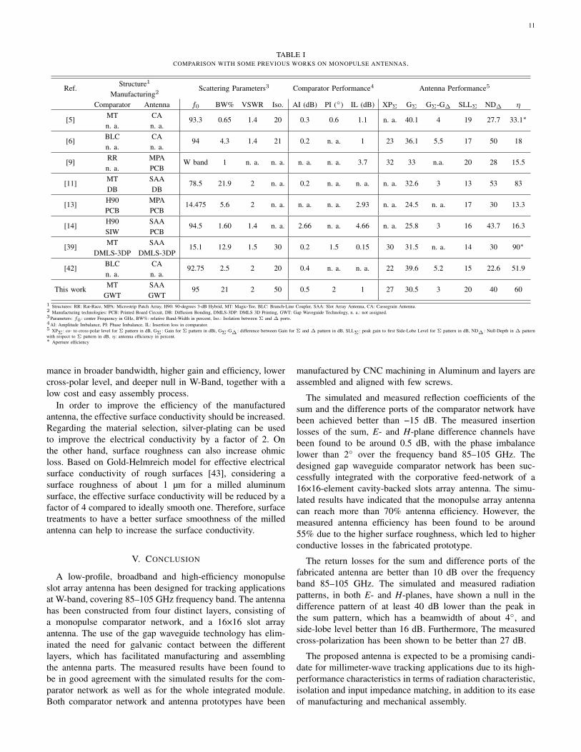
A comparison between eight published works and thepresent paper is summarized in TABLE I. Since the presentpaper is the first gap waveguide-based monopulse antenna,TABLE I shows a comparison between different technologiesin terms of scattering parameters (matching and isolation),comparator network parameters (imbalances and loss), andradiation parameters (gain, side-lobes, cross-polarization, andefficiency).
As the proposed antenna benefits from using waveguide-based corporate feeding network, it offers 21% input reflection

10
−90 −60 −30 0 30 60 90−60
−40
−20
0
Angle (deg)
Rel
ativ
eA
mpl
itud
e(d
B)
Sim. Σ
Sim. ∆ E -planeMeas. Σ
Meas. ∆ E -plane
(a)
−90 −60 −30 0 30 60 90−60
−40
−20
0
Angle (deg)
Rel
ativ
eA
mpl
itud
e(d
B)
Sim. Σ
Sim. ∆ H -planeMeas. Σ
Meas. ∆ H -plane
(b)
−90 −60 −30 0 30 60 90−60
−40
−20
0
Angle (deg)
Rel
ativ
eA
mpl
itud
e(d
B)
Sim. Σ
Sim. ∆ E -planeMeas. Σ
Meas. ∆ E -plane
(c)
−90 −60 −30 0 30 60 90−60
−40
−20
0
Angle (deg)
Rel
ativ
eA
mpl
itud
e(d
B)
Sim. Σ
Sim. ∆ H -planeMeas. Σ
Meas. ∆ H -plane
(d)
−90 −60 −30 0 30 60 90−60
−40
−20
0
Angle (deg)
Rel
ativ
eA
mpl
itud
e(d
B)
Sim. Σ
Sim. ∆ E -planeMeas. Σ
Meas. ∆ E -plane
(e)
−90 −60 −30 0 30 60 90−60
−40
−20
0
Angle (deg)
Rel
ativ
eA
mpl
itud
e(d
B)
Sim. Σ
Sim. ∆ H -planeMeas. Σ
Meas. ∆ H -plane
(f)Fig. 27. Simulated and measured normalized sum and difference radiationpattern of the proposed monopulse antenna. (a) E-plane at 90 GHz. (b) H-plane at 90 GHz. (c) E-plane at 95 GHz. (d) H-plane at 95 GHz. (e) E-planeat 100 GHz. (f) H-plane at 100 GHz.
86 88 90 92 94 96 98 100 102 10422
24
26
28
30
32
34
η = 70%
η = 60%
η = 50%
Frequency (GHz)
Co-
pola
rG
ain
(dB
i)
86 88 90 92 94 96 98 100 102 104−5
0
5
10
15
20
25
Cro
ss-p
olar
Gai
n(d
Bi)
Sim. Co-pol. Meas. Co-pol. Sim. X-pol. Meas. X-pol.
Fig. 28. Simulated and measured gains of the sum beam of the proposedantenna.
coefficient bandwidth. Also, compared to other works, the bestisolation (50 dB) between the sum and difference ports hasbeen achieved, which is better than [39] that uses Direct MetalLaser Sintering (DMLS) metal 3D printing. Good isolationin the proposed Magic-Tee makes it possible to have highisolation. It should be noted that due to the limited spacebetween the input ports of the proposed antenna, it was notpossible to measure the isolation between the ports. However,by increasing the length of the transmission lines on Layer 3(see Fig. 19(d)), it is possible to achieve the required separa-tion to accommodate standard flanges without any significanteffect on the antenna performance.
The proposed monopulse comparator network in this paperoffers a total loss less than 1.5 dB which is close to hollowwaveguide design in [39] and lower than PCB- and SIW-baseddesigns in [9], [13], [14]. The measured 1.5 dB loss in thecomparator network also contains the first two power divisionstages of the feed-network. The measured performance ofthe fabricated comparator network is compared with someavailable works in TABLE I.
The low-loss comparator and the designed array have en-abled the realization of a high-efficiency antenna. TABLE Ishows that the efficiency of the proposed antenna system ismuch higher than PCB-, SIW-, and reflector-based antennasin [5], [6], [9], [13], [14], [42]. The simulated efficiency ofthe monopulse antenna that is based on hollow waveguidetechnology in [11] will decrease due to the higher conductiveloss after manufacturing. Moreover, in [39] only the apertureefficiency was presented. For the other radiation parameters,like gain, cross-polar level and side-lobe level in the sumpattern, and depth of the null in difference patterns, theproposed antenna parameters are between those based onhollow waveguide designs manufactured by using diffusionbonding and DMLS manufacturing processes.
TABLE I indicates that among all technologies that havebeen used for manufacturing monopulse antennas, the gapwaveguide technology can offer an excellent tracking perfor-
11
TABLE ICOMPARISON WITH SOME PREVIOUS WORKS ON MONOPULSE ANTENNAS.
Ref. Structure1
Manufacturing2Scattering Parameters3 Comparator Performance4 Antenna Performance5
Comparator Antenna f0 BW% VSWR Iso. AI (dB) PI (◦) IL (dB) XPΣ GΣ GΣ-G∆ SLLΣ ND∆ η
[5] MTn. a.
CAn. a.
93.3 0.65 1.4 20 0.3 0.6 1.1 n. a. 40.1 4 19 27.7 33.1∗
[6] BLCn. a.
CAn. a.
94 4.3 1.4 21 0.2 n. a. 1 23 36.1 5.5 17 50 18
[9] RRn. a.
MPAPCB
W band 1 n. a. n. a. n. a. n. a. 3.7 32 33 n.a. 20 28 15.5
[11] MTDB
SAADB
78.5 21.9 2 n. a. 0.2 n. a. n. a. n. a. 32.6 3 13 53 83
[13] H90PCB
MPAPCB
14.475 5.6 2 n. a. n. a. n. a. 2.93 n. a. 24.5 n. a. 17 30 13.3
[14] H90SIW
SAAPCB
94.5 1.60 1.4 n. a. 2.66 n. a. 4.66 n. a. 25.8 3 16 43.7 16.3
[39] MTDMLS-3DP
SAADMLS-3DP
15.1 12.9 1.5 30 0.2 1.5 0.15 30 31.5 n. a. 14 30 90∗
[42] BLCn. a.
CAn. a.
92.75 2.5 2 20 0.4 n. a. n. a. 22 39.6 5.2 15 22.6 51.9
This work MTGWT
SAAGWT
95 21 2 50 0.5 2 1 27 30.5 3 20 40 60
1 Structures: RR: Rat-Race, MPA: Microstrip Patch Array, H90: 90-degrees 3-dB Hybrid, MT: Magic-Tee, BLC: Branch-Line Coupler, SAA: Slot Array Antenna, CA: Cassegrain Antenna.2 Manufacturing technologies: PCB: Printed Board Circuit, DB: Diffusion Bonding, DMLS-3DP: DMLS 3D Printing, GWT: Gap Waveguide Technology, n. a.: not assigned.3Parameters: f0 : center Frequency in GHz, BW%: relative Band-Width in percent, Iso.: Isolation between Σ and ∆ ports.4AI: Amplitude Imbalance, PI: Phase Imbalance, IL: Insertion loss in comparator.5 XPΣ : co- to cross-polar level for Σ pattern in dB, GΣ : Gain for Σ pattern in dBi, GΣ -G∆ : difference between Gain for Σ and ∆ pattern in dB, SLLΣ : peak gain to first Side-Lobe Level for Σ pattern in dB, ND∆ : Null-Depth in ∆ patternwith respect to Σ pattern in dB, η: antenna efficiency in percent.∗ Aperture efficiency
mance in broader bandwidth, higher gain and efficiency, lowercross-polar level, and deeper null in W-Band, together with alow cost and easy assembly process.
In order to improve the efficiency of the manufacturedantenna, the effective surface conductivity should be increased.Regarding the material selection, silver-plating can be usedto improve the electrical conductivity by a factor of 2. Onthe other hand, surface roughness can also increase ohmicloss. Based on Gold-Helmreich model for effective electricalsurface conductivity of rough surfaces [43], considering asurface roughness of about 1 µm for a milled aluminumsurface, the effective surface conductivity will be reduced by afactor of 4 compared to ideally smooth one. Therefore, surfacetreatments to have a better surface smoothness of the milledantenna can help to increase the surface conductivity.
V. CONCLUSION
A low-profile, broadband and high-efficiency monopulseslot array antenna has been designed for tracking applicationsat W-band, covering 85–105 GHz frequency band. The antennahas been constructed from four distinct layers, consisting ofa monopulse comparator network, and a 16×16 slot arrayantenna. The use of the gap waveguide technology has elim-inated the need for galvanic contact between the differentlayers, which has facilitated manufacturing and assemblingthe antenna parts. The measured results have been found tobe in good agreement with the simulated results for the com-parator network as well as for the whole integrated module.Both comparator network and antenna prototypes have been
manufactured by CNC machining in Aluminum and layers areassembled and aligned with few screws.
The simulated and measured reflection coefficients of thesum and the difference ports of the comparator network havebeen achieved better than −15 dB. The measured insertionlosses of the sum, E- and H-plane difference channels havebeen found to be around 0.5 dB, with the phase imbalancelower than 2◦ over the frequency band 85–105 GHz. Thedesigned gap waveguide comparator network has been suc-cessfully integrated with the corporative feed-network of a16×16-element cavity-backed slots array antenna. The simu-lated results have indicated that the monopulse array antennacan reach more than 70% antenna efficiency. However, themeasured antenna efficiency has been found to be around55% due to the higher surface roughness, which led to higherconductive losses in the fabricated prototype.
The return losses for the sum and difference ports of thefabricated antenna are better than 10 dB over the frequencyband 85–105 GHz. The simulated and measured radiationpatterns, in both E- and H-planes, have shown a null in thedifference pattern of at least 40 dB lower than the peak inthe sum pattern, which has a beamwidth of about 4◦, andside-lobe level better than 16 dB. Furthermore, The measuredcross-polarization has been shown to be better than 27 dB.
The proposed antenna is expected to be a promising candi-date for millimeter-wave tracking applications due to its high-performance characteristics in terms of radiation characteristic,isolation and input impedance matching, in addition to its easeof manufacturing and mechanical assembly.

12
REFERENCES
[1] D. Liu, U. Pfeiffer, J. Grzyb, and B. Gaucher, Advanced millimeter-wavetechnologies: antennas, packaging and circuits. John Wiley & Sons,2009.
[2] B. Cao, H. Wang, Y. Huang, and J. Zheng, “High-gain L-probe ex-cited substrate integrated cavity antenna array with LTCC-based gapwaveguide feeding network for W-band application,” Antennas andPropagation, IEEE Transactions on, vol. 63, no. 12, pp. 5465–5474,2015.
[3] S. M. Sherman and D. K. Barton, Monopulse principles and techniques.Artech House, 2011.
[4] S. Raman, N. S. Barker, and G. M. Rebeiz, “A W-band dielectric-lens-based integrated monopulse radar receiver,” IEEE Transactions onMicrowave Theory and Techniques, vol. 46, no. 12, pp. 2308–2316,1998.
[5] Y. Wang, W. Dou, and B. Bi, “W band axially displaced monopulse dual-reflector antenna for inter-satellite communications,” IET Microwaves,Antennas & Propagation, vol. 10, no. 7, pp. 742–747, 2016.
[6] P. Zheng, G. Q. Zhao, S. H. Xu, F. Yang, and H. J. Sun, “Design of a W-band full-polarization monopulse Cassegrain antenna,” IEEE Antennasand Wireless Propagation Letters, vol. 16, pp. 99–103, 2017.
[7] A. Haddadi and A. Ghorbani, “Distorted reflector antennas: Analysis ofradiation pattern and polarization performance,” IEEE Transactions onAntennas and Propagation, vol. 64, no. 10, pp. 4159–4167, 2016.
[8] A. Haddadi, A. Ghorbani, and P. Taghikhani, “Distorted reflector anten-nas: fast and accurate estimation of the surface distortion profile using anew formula,” IET Microwaves, Antennas & Propagation, vol. 11, no. 9,pp. 1248–1254, 2017.
[9] D. Jahagirdar and J. Prasad, “A W-band trans-twist monopulse mi-crostrip patch reflectarray,” in Radar Conference, 2005. EURAD 2005.European. IEEE, 2005, pp. 197–199.
[10] T. Tomura, J. Hirokawa, T. Hirano, and M. Ando, “A 45◦ linearlypolarized hollow-waveguide 16×16-slot array antenna covering 71–86GHz band,” IEEE Transactions on Antennas and Propagation, vol. 62,no. 10, pp. 5061–5067, 2014.
[11] X. Xu, J. Hirokawa, and M. Ando, “An E-band slotted waveguidemonopulse array antenna with corporate-feed using diffusion bondingof laminated plates,” in Antennas and Propagation (ISAP), 2016 Inter-national Symposium on. IEEE, 2016, pp. 308–309.
[12] A. Vosoogh, P.-S. Kildal, and V. Vassilev, “Wideband and high-gaincorporate-fed gap waveguide slot array antenna with ETSI class IIradiation pattern in V-band,” IEEE Transactions on Antennas andPropagation, 2016.
[13] H. Wang, D.-G. Fang, and X. Chen, “A compact single layer monopulsemicrostrip antenna array,” IEEE Transactions on antennas and propa-gation, vol. 54, no. 2, pp. 503–509, 2006.
[14] Y. J. Cheng, W. Hong, and K. Wu, “94 GHz substrate integratedmonopulse antenna array,” IEEE Transactions on Antennas and Propa-gation, vol. 60, no. 1, pp. 121–129, 2012.
[15] T. Li, W. Dou, and H. Meng, “A monopulse slot array antenna basedon dual-layer substrate integrated waveguide (SIW),” in Antennas andPropagation (APCAP), 2016 IEEE 5th Asia-Pacific Conference on.IEEE, 2016, pp. 373–374.
[16] P.-S. Kildal, “Artificially soft and hard surfaces in electromagnetics,”Antennas and Propagation, IEEE Transactions on, vol. 38, no. 10, pp.1537–1544, 1990.
[17] P.-S. Kildal, A. U. Zaman, E. Rajo-Iglesias, E. Alfonso, and A. Valero-Nogueira, “Design and experimental verification of ridge gap waveguidein bed of nails for parallel-plate mode suppression,” IET Microwaves,Antennas & Propagation, vol. 5, no. 3, pp. 262–270, Feb. 2011.
[18] A. A. Brazalez, E. Rajo-Iglesias, J. L. Vazquez-Roy, A. Vosoogh, and P.-S. Kildal, “Design and validation of microstrip gap waveguides and theirtransitions to rectangular waveguide, for millimeter-wave applications,”Microwave Theory and Techniques, IEEE Transactions on, vol. 63,no. 12, pp. 4035–4050, 2015.
[19] E. Rajo-Iglesias and P.-S. Kildal, “Groove gap waveguide: A rectangularwaveguide between contactless metal plates enabled by parallel-platecut-off,” in Antennas and Propagation (EuCAP), 2010 Proceedings ofthe Fourth European Conference on. IEEE, 2010, pp. 1–4.
[20] A. Vosoogh and P.-S. Kildal, “Corporate-fed planar 60 GHz slot arraymade of three unconnected metal layers using AMC pin surface forthe gap waveguide,” IEEE Antennas and Wireless Propagation Letters,vol. 15, pp. 1935–1938, Dec. 2015.
[21] ——, “High efficiency 2 × 2 cavity-backed slot sub-array for 60 GHzplanar array antenna based on gap technology,” in 2015 International
Symposium on Antennas and Propagation (ISAP). IEEE, 2015, pp.1–3.
[22] A. Vosoogh, P.-S. Kildal, and V. Vassilev, “A multi-layer gap waveguidearray antenna suitable for manufactured by die-sink EDM,” in 2016 10thEuropean Conference on Antennas and Propagation (EuCAP). IEEE,2016, pp. 1–4.
[23] A. Vosoogh and P.-S. Kildal, “V-band high efficiency corporate-fed8× 8 slot array antenna with ETSI class II radiation pattern based ongap technology,” in Antennas and Propagation (APSURSI), 2016 IEEEInternational Symposium on. IEEE, 2016, pp. 803–804.
[24] H. Attia, M. S. Sorkherizi, and A. A. Kishk, “60 GHz slot antennaarray based on ridge gap waveguide technology enhanced with dielec-tric superstrate,” in 2015 9th European Conference on Antennas andPropagation (EuCAP). IEEE, 2015, pp. 1–4.
[25] S. A. Razavi, P.-S. Kildal, L. Xiang, E. Alfonso Alos, and H. Chen,“2 × 2-slot element for 60-GHz planar array antenna realized on twodoubled-sided pcbs using SIW cavity and EBG-type soft surface fedby microstrip-ridge gap waveguide,” Antennas and Propagation, IEEETransactions on, vol. 62, no. 9, pp. 4564–4573, Sep. 2014.
[26] A. Vosoogh, A. A. Brazalez, and P.-S. Kildal, “A V-band invertedmicrostrip gap waveguide end-coupled bandpass filter,” IEEE Microwaveand Wireless Components Letters, vol. 26, no. 4, pp. 261–263, Apr. 2016.
[27] M. S. Sorkherizi, A. Khaleghi, and P.-S. Kildal, “Direct-coupled cavityfilter in ridge gap waveguide,” IEEE Transactions on Components,Packaging and Manufacturing Technology, vol. 4, no. 3, pp. 490–495,Mar. 2014.
[28] A. Berenguer, M. Baquero-Escudero, D. Sanchez-Escuderos,B. Bernardo-Clemente, and V. E. Boria-Esbert, “Low insertion loss 61GHz narrow-band filter implemented with groove gap waveguides,” inMicrowave Conference (EuMC), 2014 44th European. IEEE, 2014,pp. 191–194.
[29] E. A. Alos, A. U. Zaman, and P.-S. Kildal, “Ka-band gap waveguidecoupled-resonator filter for radio link diplexer application,” IEEE Trans-actions on Components, Packaging and Manufacturing Technology,vol. 3, no. 5, pp. 870–879, 2013.
[30] M. S. Sorkherizi and A. A. Kishk, “Fully printed Gap waveguide with fa-cilitated design properties,” IEEE Microwave and Wireless ComponentsLetters, vol. 26, no. 9, pp. 657–659, 2016.
[31] M. Rezaee, A. U. Zaman, and P.-S. Kildal, “A groove gap waveguideiris filter for V-band application,” in 2015 23rd Iranian Conference onElectrical Engineering. IEEE, 2015, pp. 462–465.
[32] M. S. Sorkherizi and A. A. Kishk, “Completely tuned coupled cavity fil-ters in defected bed of nails cavity,” IEEE Transactions on Components,Packaging and Manufacturing Technology, 2016.
[33] A. Vosoogh, M. S. Sorkherizi, A. U. Zaman, J. Yang, and A. A.Kishk, “An integrated Ka-band diplexer-antenna array module basedon gap waveguide technology with simple mechanical assembly andno electrical contact requirements,” IEEE Transactions on MicrowaveTheory and Techniques, vol. 66, no. 2, pp. 962–972, 2018.
[34] M. Rezaee, A. U. Zaman, and P.-S. Kildal, “V-band groove gapwaveguide diplexer,” in Antennas and Propagation (EuCAP), 2015 9thEuropean Conference on. IEEE, 2015, pp. 1–4.
[35] A. Vosoogh, M. S. Sorkherizi, A. U. Zaman, J. Yang, and A. A. Kishk,“An E-band antenna-diplexer compact integrated solution based on gapwaveguide technology,” in Antennas and Propagation (ISAP), 2017International Symposium on. IEEE, 2017, pp. 1–2.
[36] ——, “Diplexer integration into a Ka-band high-gain gap waveguidecorporate-fed slot array antenna,” in Antennas and Propagation &USNC/URSI National Radio Science Meeting, 2017 IEEE InternationalSymposium on. IEEE, 2017, pp. 2667–2668.
[37] A. U. Zaman and P.-S. Kildal, “Wide-band slot antenna arrays withsingle-layer corporate-feed network in ridge gap waveguide technology,”IEEE Transactions on Antennas and Propagation, vol. 62, no. 6, pp.2992–3001, Jun 2014.
[38] A. Vosoogh, P.-S. Kildal, V. Vassilev, A. U. Zaman, and S. Carlsson,“E-band 3-D metal printed wideband planar horn array antenna,” inAntennas and Propagation (ISAP), 2016 International Symposium on,2016.
[39] G.-L. Huang, S.-G. Zhou, and T.-H. Chio, “Highly-efficient self-compactmonopulse antenna system with integrated comparator network for RFindustrial applications,” IEEE Transactions on Industrial Electronics,vol. 64, no. 1, pp. 674–681, 2017.
[40] A. Vosoogh, A. U. Zaman, and V. Vassilev, “Wideband cavity-backedslot subarray with gap waveguide feed-network for D-band applications,”in Antennas and Propagation (EUCAP), 2017 11th European Confer-ence on. IEEE, 2017, pp. 207–209.

13
[41] T. Tomura, Y. Miura, M. Zhang, J. Hirokawa, and M. Ando, “A 45◦linearly polarized hollow-waveguide corporate-feed slot array antennain the 60-GHz band,” Antennas and Propagation, IEEE Transactionson, vol. 60, no. 8, pp. 3640–3646, 2012.
[42] P. Zheng, B. Hu, S. Xu, and H. Sun, “A W-band high-aperture-efficiencymultipolarized monopulse cassegrain antenna fed by phased microstrippatch quad,” IEEE Antennas and Wireless Propagation Letters, vol. 16,pp. 1609–1613, 2017.
[43] G. Gold and K. Helmreich, “A physical surface roughness model and itsapplications,” IEEE Transactions on Microwave Theory and Techniques,vol. 65, no. 10, pp. 3720–3732, 2017.
Abbas Vosoogh received the B.Sc. degree in elec-trical engineering from the University of Sistan andBaluchestan, Zahedan, Iran, and the M.Sc. degreefrom K. N. Toosi University of Technology, Tehran,Iran, in 2008 and 2011, respectively. He is cur-rently pursuing his Ph.D. degree with ChalmersUniversity of Technology, Gothenburg, Sweden. Hiscurrent research interests include the development ofgap waveguide technology for millimeter and sub-millimeter wave applications, microwave passivecomponents, EBG, soft and hard surfaces, mm-wave
planar array antennas, and integration of passive and active components witharray antenna.
Mr. Vosoogh was a recipient of the Best Student Paper Award of the 2015International Symposium on Antennas and Propagation, TAS, Australia, theCST University Publication Award 2016, the Best Paper Award and the BestStudent Paper Award of the 2016 International Symposium on Antennas andPropagation, Okinawa, Japan, and the First Prize Student Award of the 2017IEEE International Symposium on Antennas and Propagation and USNC-URSI Radio Science Meeting, San Diego, CA, USA.
Abolfazl Haddadi received his M. Sc and Ph. D.degrees in electrical engineering from AmirKabirUniversity of Technology (Tehran Polytechnique),Tehran, Iran, in 2010 and 2015, respectively. HisPh. D. thesis was entitled ”Reflector Antenna Sur-face Distortion Determination and Compensation.”He was an antenna engineer at Iranian Telecom-munications Research Center (ITRC) and IranianSpace Research Center (ISRC) with focus on phasedarray and reflector antennas for space applications.In March 2015, he was at Chalmers University of
Technology, Gteborg, Sweden, as a visiting researcher. Currently, he is a seniorantenna engineer at GAPWAVES AB, Gteborg, Sweden. His main researchinterests include gap waveguide-based antennas, phased array antennas, andantenna industrialization methods for mass production.
Ashraf Uz Zaman (M’14) was born in Chittagong,Bangladesh. He received the B.Sc. degree in electri-cal and electronics engineering from the ChittagongUniversity of Engineering and Technology, Chit-tagong. He received the M.Sc. and PhD degree fromChalmers University of Technology, Gteborg, Swe-den, in 2007 and 2013 respectively. He is currentlyan assistant professor with the Communication andAntenna Division of the same university. His currentresearch interests include millimeter wave high effi-ciency planar antennas in general, gap waveguide
technology, frequency selective surfaces, microwave passive components,packaging techniques and integration of MMICs with the antennas.
Jian Yang (M’02SM’10) received the B.Sc. degreein electrical engineering from the Nanjing Universityof Science and Technology, Nanjing, China, in 1982,the M.Sc. degree in electrical engineering from theNanjing Research Center of Electronic Engineering,Nanjing, in 1985, and the Swedish Licentiate andPh.D. degrees from Chalmers University of Tech-nology, Gothenburg, Sweden, in 1998 and 2001, re-spectively. From 1985 to 1996, he was with the Nan-jing Research Institute of Electronics Technology,Nanjing, China, as a Senior Engineer. From 1999 to
2005, he was with the Department of Electromagnetics, Chalmers Universityof Technology, Gothenburg, Sweden, as a Research Engineer. During 2005and 2006, he was with COMHAT AB as a Senior Engineer. From 2006 to2010, he was an Assistant Professor, from 2010 to 2016, he was an AssociateProfessor, and since 2016 he has been a professor with the Departmentof Signals and Systems, Chalmers University of Technology. His researchinterests include 60-140GHz antennas, terahertz antennas, MIMO antennas,ultrawideband (UWB) antennas and UWB feeds for reflector antennas, UWBradar systems,UWB antennas in near-field sensing applications, hat-fed anten-nas, reflector antennas, radome design, and computational electromagnetics.
Herbert Zirath (M’86-SM’08-F’11) was born inGoteborg, Sweden, on March 20, 1955. He receivedthe M. Sc and Ph. D. degree in electrical engineeringfrom Chalmers University, Goteborg, Sweden, in1980 and 1986, respectively. From 1986 to 1996 hewas a researcher at the Radio and Space Science atChalmers University, engaged in developing a GaAsand InP based HEMT technology, including devices,models and circuits. In the spring-summer 1998 hewas research fellow at Caltech, Pasadena, USA, en-gaged in the design of MMIC frequency multipliers
and Class E Power amplifiers. He is since 1996 Professor in High SpeedElectronics at the Department of Microtechnology and Nanoscience, MC2,at Chalmers University. He became the head of the Microwave ElectronicsLaboratory 2001. At present he is leading a group of approximately 40 re-searchers in the area of high frequency semiconductor devices and circuits. Hismain research interests include MMIC designs for wireless communicationand sensor applications based on III-V, III-N, Graphene, and silicon devices.He is author/co-author of more than 560 refereed journal/conference papers,h-index of 41, and holds 5 patents. He is research fellow at Ericsson AB,leading the development of a D-band (110-170 GHz) chipset for high datarate wireless communication. He is a co-founder of Gotmic AB, a companydeveloping highly integrated front-end MMIC chip-sets for 60 GHz and E-band wireless communication.
Ahmed A. Kishk (S’84-M’86-SM’90-F’98) re-ceived the BS degree in Electronic and Commu-nication Engineering from Cairo University, Cairo,Egypt, in 1977, and BSc. in Applied Mathematicsfrom Ain-Shams University, Cairo, Egypt, in 1980.In 1983 and 1986, he received M. Eng., and Ph.D.degrees from the Department of Electrical Engi-neering, University of Manitoba, Winnipeg, Canada,respectively. In 1986, he joined the Department ofElectrical Engineering, University of Mississippi, Hewas a Professor at the University of Mississippi
(1995-2011). Currently, he is a Professor at Concordia University, Montreal,Quebec, Canada (since 2011) as Tier 1 Canada Research Chair in AdvancedAntenna Systems. He was the 2017 AP-S president.
His research interest includes the areas of millimeter wave antennas for 5Gapplications, Analog beamforming network, Antennass, microwave passivecircuits and componenets, EBG, artificial magnetic conductors, phased arrayantennas, reflect/transmitarray, wearable antennas. He has published over 330-refereed Journal articles and 500 conference papers. He is a co-author of fourbooks and several book chapters and the editor of three books.


![Compact Triangular Slot Antenna with Improved … · Compact Triangular Slot Antenna with Improved ... .Zeland IE3D [18] ... A. Balanis, “Advanced Engineering Electromagnetics”,](https://img.pdfslide.us/doc/110x75/5acbed9e7f8b9aa1518bb8a7/compact-triangular-slot-antenna-with-improved-triangular-slot-antenna-with-improved.jpg)