Embed Size (px)
Citation preview
Paper presented at the 2013 IEEE International Ultrasonics Symposium:
Void-Free Direct Bonding of CMUTArrayswith Single Crystalline Plates and Pull-In Insulation
Thomas Lehrmann Christiansen, Ole Hansen, MathiasDahl Johnsen, Jeppe Nyskjold Lohse, Jørgen Arendt Jensenand Erik V. Thomsen
Center for Fast Ultrasound Imaging,Biomedical Engineering Group,Department of Electrical EngineeringØrsteds Plads Building 349,Technical University of Denmark,2800 Kgs. Lyngby, Denmark.
To be published in the 2013 IEEE International Ultrasonics Symposium Proceedings.
Void-Free Direct Bonding of CMUT Arrays withSingle Crystalline Plates and Pull-In Insulation
Thomas Lehrmann Christiansen∗,Ole Hansen∗, Mathias Dahl Johnsen∗, Jeppe Nyskjold Lohse∗, Jørgen Arendt Jensen† and Erik V. Thomsen∗∗Department of Micro- and Nanotechnology, Technical University of Denmark, DK-2800 Kgs. Lyngby, Denmark
†Center for Fast Ultrasound Imaging, Department of Electrical Engineering,Technical University of Denmark, DK-2800 Kgs. Lyngby, Denmark
Abstract—The implications on direct bonding quality, when us-ing a double oxidation step to fabricate capacitive micromachinedultrasonic transducers (CMUTs), is analyzed. The protrusionsalong the CMUT cavity edges created during the second oxi-dation are investigated using simulations, AFM measurements,and a proposed analytical model, which is in good agreementwith the simulated results. The results demonstrate protrusionheights in the order of 10 nm to 40 nm, with higher oxidationtemperatures giving the highest protrusions. Isotropically wetetched cavities exhibit significantly smaller protrusions thananisotropically plasma etched cavities after the second oxidation.It is demonstrated that the protrusions will prevent good waferbonding without subsequent polishing or etching steps. A newfabrication process is therefore proposed, allowing protrusion-free bonding surfaces with no alteration of the final structureand no additional fabrication steps compared to the doubleoxidation process. Two identical CMUT arrays with circular andsquare cavities having diameter/side lengths of 72 µm/65 µm anda 20 µm interdistance are fabricated with the two processes,demonstrating void-free bonding and 100 % yield from theproposed process compared to poor bonding and 7 % yield usingthe double oxidation process.
I. INTRODUCTION
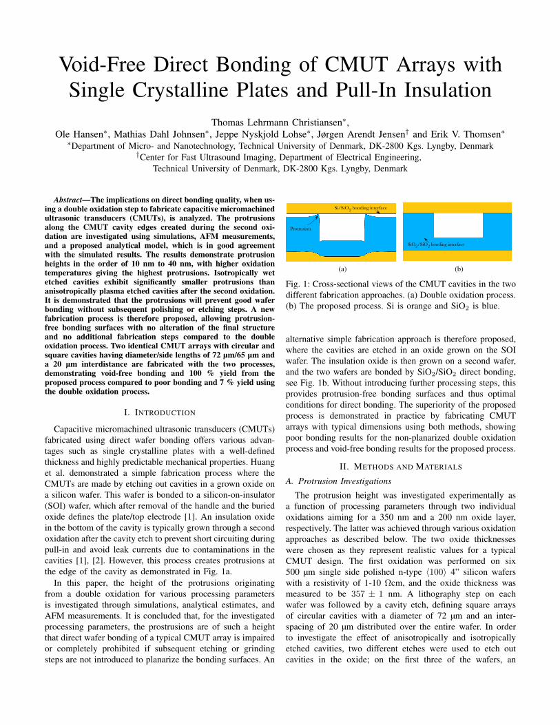
Capacitive micromachined ultrasonic transducers (CMUTs)fabricated using direct wafer bonding offers various advan-tages such as single crystalline plates with a well-definedthickness and highly predictable mechanical properties. Huanget al. demonstrated a simple fabrication process where theCMUTs are made by etching out cavities in a grown oxide ona silicon wafer. This wafer is bonded to a silicon-on-insulator(SOI) wafer, which after removal of the handle and the buriedoxide defines the plate/top electrode [1]. An insulation oxidein the bottom of the cavity is typically grown through a secondoxidation after the cavity etch to prevent short circuiting duringpull-in and avoid leak currents due to contaminations in thecavities [1], [2]. However, this process creates protrusions atthe edge of the cavity as demonstrated in Fig. 1a.
In this paper, the height of the protrusions originatingfrom a double oxidation for various processing parametersis investigated through simulations, analytical estimates, andAFM measurements. It is concluded that, for the investigatedprocessing parameters, the prostrusions are of such a heightthat direct wafer bonding of a typical CMUT array is impairedor completely prohibited if subsequent etching or grindingsteps are not introduced to planarize the bonding surfaces. An
Protrusion
Si/SiO2 bonding interface
(a)
SiO2/SiO2 bonding interface
(b)
Fig. 1: Cross-sectional views of the CMUT cavities in the twodifferent fabrication approaches. (a) Double oxidation process.(b) The proposed process. Si is orange and SiO2 is blue.
alternative simple fabrication approach is therefore proposed,where the cavities are etched in an oxide grown on the SOIwafer. The insulation oxide is then grown on a second wafer,and the two wafers are bonded by SiO2/SiO2 direct bonding,see Fig. 1b. Without introducing further processing steps, thisprovides protrusion-free bonding surfaces and thus optimalconditions for direct bonding. The superiority of the proposedprocess is demonstrated in practice by fabricating CMUTarrays with typical dimensions using both methods, showingpoor bonding results for the non-planarized double oxidationprocess and void-free bonding results for the proposed process.
II. METHODS AND MATERIALS
A. Protrusion Investigations
The protrusion height was investigated experimentally asa function of processing parameters through two individualoxidations aiming for a 350 nm and a 200 nm oxide layer,respectively. The latter was achieved through various oxidationapproaches as described below. The two oxide thicknesseswere chosen as they represent realistic values for a typicalCMUT design. The first oxidation was performed on six500 µm single side polished n-type 〈100〉 4” silicon waferswith a resistivity of 1-10 Ωcm, and the oxide thickness wasmeasured to be 357 ± 1 nm. A lithography step on eachwafer was followed by a cavity etch, defining square arraysof circular cavities with a diameter of 72 µm and an inter-spacing of 20 µm distributed over the entire wafer. In orderto investigate the effect of anisotropically and isotropicallyetched cavities, two different etches were used to etch outcavities in the oxide; on the first three of the wafers, an
Protrusion height
h
(a)
450
nm
200
nm
(b)
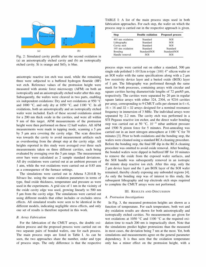
Fig. 2: Simulated cavity profile after the second oxidation in(a) an anisotropically etched cavity and (b) an isotropicallyetched cavity. Si is orange and SiO2 is blue.
anisotropic reactive ion etch was used, while the remainingthree were subjected to a buffered hydrogen flouride (HF)wet etch. Reference values of the protrusion height weremeasured with atomic force microscopy (AFM) on both anisotropically and an anisotropically etched wafer after this step.Subsequently, the wafers were cleaved in two parts, enablingsix independent oxidations: Dry and wet oxidations at 950 Cand 1000 C, and only dry at 1050 C, and 1100 C. In alloxidations, both an anisotropically and an isotropically etchedwafer were included. Each of these second oxidations aimedfor a 200 nm thick oxide in the cavities, and were all within9 nm of this target. AFM measurements of the protrusionheight were then performed on these 12 half wafers. All AFMmeasurements were made in tapping mode, scanning a 5 µmby 5 µm area covering the cavity edge. The scan directionwas towards the cavity to avoid measurement artifacts suchas overshooting from the abrupt step at the cavity edge. Allheights reported in this study were averaged over three suchmeasurements taken on three different cavities, each beingevaluated by averaging over the 5 µm range. The measurementerror bars were calculated as 2 sample standard deviations.All dry oxidations were carried out at an ambient pressure of1 atm, while the wet oxidations were carried out at 0.85 atmas a consequence of the furnace settings.
The simulations were carried out in Athena 5.20.0.R bySilvaco Inc. using the same oxidation parameters in terms oftype, final oxide thickness, temperature and pressure as wereused in the experiments. A grid size of 1 nm in the vicinity ofthe oxide cavity edge was used, growing linearly to 500 nm5 µm from the cavity edge. The simulations were carried outusing different models that either includes or excludes stresseffects. All simulated results were seen to be identical in thedifferent models, indicating negligible stress effects, and onlyone set of results is therefore reported in this work.
B. Array Fabrication
For the fabrication of the CMUT arrays, the double oxi-dation process and the proposed process were carried out ontwo separate pairs of bonded wafers, one for each process.The main process steps are listed in Table I. As can beseen, the two approaches share the number, order and typeof process steps. The only difference is that the respective
TABLE I: A list of the main process steps used in bothfabrication approaches. For each step, the wafer on which theprocess step is carried out in the respective approach is given.
Step Double oxidation Proposed process
403 nm oxidation Standard SOILithography Standard SOICavity etch Standard SOI195 nm oxidation Standard StandardBonding Standard/SOI Standard/SOIHandle removal SOI SOI
process steps were carried out on either a standard, 500 µmsingle side polished 1-10 Ωcm n-type 〈100〉 4” silicon wafer oran SOI wafer with the same specifications along with a 2 µmlow resistivity device layer and a buried oxide (BOX) layerof 1 µm. The lithography was performed through the samemask for both processes, containing arrays with circular andsquare cavities having diameter/side lengths of 72 µm/65 µm,respectively. The cavities were separated by 20 µm in regularsquare lattice arrays with either 324, 2304, or 9216 cavitiesper array, corresponding to 9 CMUT cells per element in 6×6,16× 16 and 32× 32 arrays designed for a nominal resonancefrequency in immersion of 3 MHz. The individual arrays wereseparated by 2.2 mm. The cavity etch was performed in aSTI Pegasus reactive ion etcher, and the direct wafer bondingstep was carried out at 50 C, 10−3 mbar ambient pressureand 1500 N piston force for 5 minutes. Post-annealing wascarried out in an inert nitrogen atmosphere at 1100 C for 70minutes [3]. Prior to both oxidations and the bonding step, thewafers were cleaned using a standard RCA cleaning procedure.Before the bonding step, the final HF dip in the RCA cleaningprocedure was omitted to avoid oxide removal. After bonding,the bonded wafers were dipped in buffered HF for 10 minutesto remove the oxide from the exposed wafer surfaces, andthe SOI handle was subsequently removed in an isotropic40 minute deep reactive ion etch. After this step, only the2 µm device layer and the 1 µm BOX layer of the SOI waferremained, thereby clearly exposing any unbonded regions [4].As only the bonding step was of interest to this study, thesubsequent lithography and top electrode etch steps requiredto complete the CMUT arrays were not performed.
III. RESULTS AND DISCUSSION
A. Protrusion Investigations
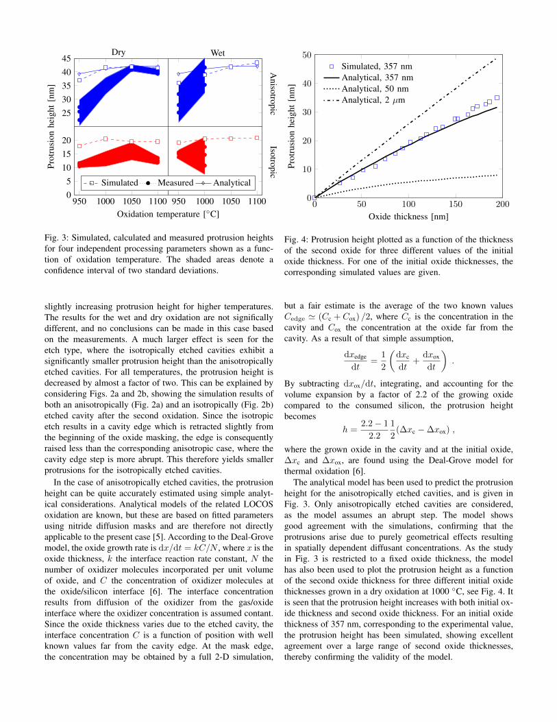
In Fig. 3, the measured protrusion heights are shown as afunction of temperature. For each temperature, both wet anddry oxidation results are shown for both anisotropically andisotropically etched cavities. No measurements are given forwet oxidations at 1050 C and 1100 C as the required oxi-dation time to reach 200 nm is impractically short. Note thatthe simulations predict higher protrusions than the measuredin most cases, the deviation being 7 nm at the most. Yet, bothsimulations and measurements agree on the general parameterdependency. It is thus seen that the oxidation temperatureonly has a minor effect on the protrusion height, with a
950 1000 1050 1100 950 1000 1050 110005
101520
2530354045
Dry Wet
Anisotropic
Isotropic
Oxidation temperature [C]
Prot
rusi
onhe
ight
[nm
]
Simulated Measured Analytical
Fig. 3: Simulated, calculated and measured protrusion heightsfor four independent processing parameters shown as a func-tion of oxidation temperature. The shaded areas denote aconfidence interval of two standard deviations.
slightly increasing protrusion height for higher temperatures.The results for the wet and dry oxidation are not significallydifferent, and no conclusions can be made in this case basedon the measurements. A much larger effect is seen for theetch type, where the isotropically etched cavities exhibit asignificantly smaller protrusion height than the anisotropicallyetched cavities. For all temperatures, the protrusion height isdecreased by almost a factor of two. This can be explained byconsidering Figs. 2a and 2b, showing the simulation results ofboth an anisotropically (Fig. 2a) and an isotropically (Fig. 2b)etched cavity after the second oxidation. Since the isotropicetch results in a cavity edge which is retracted slightly fromthe beginning of the oxide masking, the edge is consequentlyraised less than the corresponding anisotropic case, where thecavity edge step is more abrupt. This therefore yields smallerprotrusions for the isotropically etched cavities.
In the case of anisotropically etched cavities, the protrusionheight can be quite accurately estimated using simple analyt-ical considerations. Analytical models of the related LOCOSoxidation are known, but these are based on fitted parametersusing nitride diffusion masks and are therefore not directlyapplicable to the present case [5]. According to the Deal-Grovemodel, the oxide growth rate is dx/dt = kC/N , where x is theoxide thickness, k the interface reaction rate constant, N thenumber of oxidizer molecules incorporated per unit volumeof oxide, and C the concentration of oxidizer molecules atthe oxide/silicon interface [6]. The interface concentrationresults from diffusion of the oxidizer from the gas/oxideinterface where the oxidizer concentration is assumed contant.Since the oxide thickness varies due to the etched cavity, theinterface concentration C is a function of position with wellknown values far from the cavity edge. At the mask edge,the concentration may be obtained by a full 2-D simulation,
0 50 100 150 2000
10
20
30
40
50
Oxide thickness [nm]
Prot
rusi
onhe
ight
[nm
]
Simulated, 357 nmAnalytical, 357 nmAnalytical, 50 nmAnalytical, 2 µm
Fig. 4: Protrusion height plotted as a function of the thicknessof the second oxide for three different values of the initialoxide thickness. For one of the initial oxide thicknesses, thecorresponding simulated values are given.
but a fair estimate is the average of the two known valuesCedge ' (Cc + Cox) /2, where Cc is the concentration in thecavity and Cox the concentration at the oxide far from thecavity. As a result of that simple assumption,
dxedge
dt=
1
2
(dxc
dt+
dxox
dt
).
By subtracting dxox/dt, integrating, and accounting for thevolume expansion by a factor of 2.2 of the growing oxidecompared to the consumed silicon, the protrusion heightbecomes
h =2.2− 1
2.2
1
2(∆xc −∆xox) ,
where the grown oxide in the cavity and at the initial oxide,∆xc and ∆xox, are found using the Deal-Grove model forthermal oxidation [6].
The analytical model has been used to predict the protrusionheight for the anisotropically etched cavities, and is given inFig. 3. Only anisotropically etched cavities are considered,as the model assumes an abrupt step. The model showsgood agreement with the simulations, confirming that theprotrusions arise due to purely geometrical effects resultingin spatially dependent diffusant concentrations. As the studyin Fig. 3 is restricted to a fixed oxide thickness, the modelhas also been used to plot the protrusion height as a functionof the second oxide thickness for three different initial oxidethicknesses grown in a dry oxidation at 1000 C, see Fig. 4. Itis seen that the protrusion height increases with both initial ox-ide thickness and second oxide thickness. For an initial oxidethickness of 357 nm, corresponding to the experimental value,the protrusion height has been simulated, showing excellentagreement over a large range of second oxide thicknesses,thereby confirming the validity of the model.
B. Array Fabrication
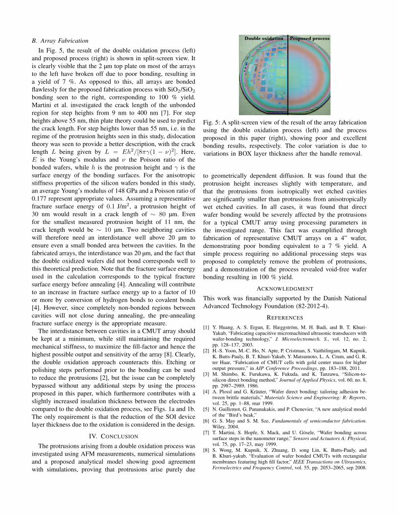
In Fig. 5, the result of the double oxidation process (left)and proposed process (right) is shown in split-screen view. Itis clearly visible that the 2 µm top plate on most of the arraysto the left have broken off due to poor bonding, resulting ina yield of 7 %. As opposed to this, all arrays are bondedflawlessly for the proposed fabrication process with SiO2/SiO2
bonding seen to the right, corresponding to 100 % yield.Martini et al. investigated the crack length of the unbondedregion for step heights from 9 nm to 400 nm [7]. For stepheights above 55 nm, thin plate theory could be used to predictthe crack length. For step heights lower than 55 nm, i.e. in theregime of the protrusion heights seen in this study, dislocationtheory was seen to provide a better description, with the cracklength L being given by L = Eh2/[8πγ(1 − ν)2]. Here,E is the Young’s modulus and ν the Poisson ratio of thebonded wafers, while h is the protrusion height and γ is thesurface energy of the bonding surfaces. For the anisotropicstiffness properties of the silicon wafers bonded in this study,an average Young’s modulus of 148 GPa and a Poisson ratio of0.177 represent appropriate values. Assuming a representativefracture surface energy of 0.1 J/m2, a protrusion height of30 nm would result in a crack length of ∼ 80 µm. Evenfor the smallest measured protrusion height of 11 nm, thecrack length would be ∼ 10 µm. Two neighboring cavitieswill therefore need an interdistance well above 20 µm toensure even a small bonded area between the cavities. In thefabricated arrays, the interdistance was 20 µm, and the fact thatthe double oxidized wafers did not bond corresponds well tothis theoretical prediction. Note that the fracture surface energyused in the calculation corresponds to the typical fracturesurface energy before annealing [4]. Annealing will contributeto an increase in fracture surface energy up to a factor of 10or more by conversion of hydrogen bonds to covalent bonds[4]. However, since completely non-bonded regions betweencavities will not close during annealing, the pre-annealingfracture surface energy is the appropriate measure.
The interdistance between cavities in a CMUT array shouldbe kept at a minimum, while still maintaining the requiredmechanical stiffness, to maximize the fill-factor and hence thehighest possible output and sensitivity of the array [8]. Clearly,the double oxidation approach counteracts this. Etching orpolishing steps performed prior to the bonding can be usedto reduce the protrusions [2], but the issue can be completelybypassed without any additional steps by using the processproposed in this paper, which furthermore contributes with aslightly increased insulation thickness between the electrodescompared to the double oxidation process, see Figs. 1a and 1b.The only requirement is that the reduction of the SOI devicelayer thickness due to the oxidation is considered in the design.
IV. CONCLUSION
The protrusions arising from a double oxidation process wasinvestigated using AFM measurements, numerical simulationsand a proposed analytical model showing good agreementwith simulations, proving that protrusions arise purely due
Double oxidation Proposed process
Fig. 5: A split-screen view of the result of the array fabricationusing the double oxidation process (left) and the processproposed in this paper (right), showing poor and excellentbonding results, respectively. The color variation is due tovariations in BOX layer thickness after the handle removal.
to geometrically dependent diffusion. It was found that theprotrusion height increases slightly with temperature, andthat the protrusions from isotropically wet etched cavitiesare significantly smaller than protrusions from anisotropicallywet etched cavities. In all cases, it was found that directwafer bonding would be severely affected by the protrusionsfor a typical CMUT array using processing parameters inthe investigated range. This fact was examplified throughfabrication of representative CMUT arrays on a 4” wafer,demonstrating poor bonding equivalent to a 7 % yield. Asimple process requiring no additional processing steps wasproposed to completely remove the problem of protrusions,and a demonstration of the process revealed void-free waferbonding resulting in 100 % yield.
ACKNOWLEDGMENT
This work was financially supported by the Danish NationalAdvanced Technology Foundation (82-2012-4).
REFERENCES
[1] Y. Huang, A. S. Ergun, E. Hæggstrom, M. H. Badi, and B. T. Khuri-Yakub, “Fabricating capacitive micromachined ultrasonic transducers withwafer-bonding technology,” J. Microelectromech. S., vol. 12, no. 2,pp. 128–137, 2003.
[2] H.-S. Yoon, M.-C. Ho, N. Apte, P. Cristman, S. Vaithilingam, M. Kupnik,K. Butts-Pauly, B. T. Khuri-Yakub, Y. Matsumoto, L. A. Crum, and G. R.ter Haar, “Fabrication of CMUT cells with gold center mass for higheroutput pressure,” in AIP Conference Proceedings, pp. 183–188, 2011.
[3] M. Shimbo, K. Furukawa, K. Fukuda, and K. Tanzawa, “Silicon-to-silicon direct bonding method,” Journal of Applied Physics, vol. 60, no. 8,pp. 2987–2989, 1986.
[4] A. Plossl and G. Krauter, “Wafer direct bonding: tailoring adhesion be-tween brittle materials,” Materials Science and Engineering: R: Reports,vol. 25, pp. 1–88, mar 1999.
[5] N. Guillemot, G. Pananakakis, and P. Chenevier, “A new analytical modelof the ”Bird’s beak,”
[6] G. S. May and S. M. Sze, Fundamentals of semiconductor fabrication.Wiley, 2004.
[7] T. Martini, S. Hopfe, S. Mack, and U. Gosele, “Wafer bonding acrosssurface steps in the nanometer range,” Sensors and Actuators A: Physical,vol. 75, pp. 17–23, may 1999.
[8] S. Wong, M. Kupnik, X. Zhuang, D. song Lin, K. Butts-Pauly, andB. Khuri-yakub, “Evaluation of wafer bonded CMUTs with rectangularmembranes featuring high fill factor,” IEEE Transactions on Ultrasonics,Ferroelectrics and Frequency Control, vol. 55, pp. 2053–2065, sep 2008.


![An introduction to arrays, continued. Recall from last time… public static void main ( String args[] ) { //define number of rooms final int N = 100; //define](https://img.pdfslide.us/doc/110x75/5a4d1b0f7f8b9ab05998e16e/an-introduction-to-arrays-continued-recall-from-last-time-public.jpg)