Embed Size (px)
Citation preview

VLSI DESIGN
Submitted by:
Deepak Malik
Asstt. Prof.
ECE Deptt.
Maharishi Markandeshwer Engineering College,
Maharishi Markandeshwer University,
Mullana (Ambala).24 November 2014 1

CONTENTS
INTRODUCTION
Transistor Types
MOS Transistors
Transistors as Switches
NMOS INVERTER
NMOS Depletion Mode Inverter Characteristics
CMOS inverter
CMOS Inverter Characteristics
Digital CMOS Logic Circuits
24 November 2014 2

INTRODUCTION
Integrated circuits: many transistors on one chip.
Very Large Scale Integration (VLSI)
Complementary Metal Oxide Semiconductor (CMOS)
Fast, cheap, “low-power” transistors circuits
.
24 November 2014 3

Transistor Types
Bipolar transistors
npn or pnp
Small current into very thin base layer controls large currents
between emitter and collector
Metal Oxide Semiconductor Field Effect Transistors
nMOS and pMOS MOSFETS
Voltage applied to insulated gate controls current between source
and drain
24 November 2014 4
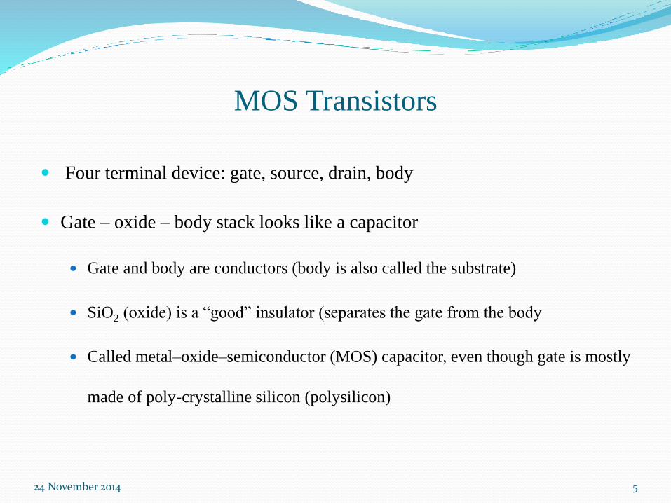
MOS Transistors
Four terminal device: gate, source, drain, body
Gate – oxide – body stack looks like a capacitor
Gate and body are conductors (body is also called the substrate)
SiO2 (oxide) is a “good” insulator (separates the gate from the body
Called metal–oxide–semiconductor (MOS) capacitor, even though gate is mostly
made of poly-crystalline silicon (polysilicon)
24 November 2014 5
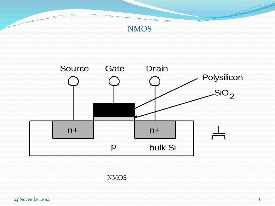
NMOS
24 November 2014 6
n+
p
GateSource Drain
bulk Si
SiO2
Polysilicon
n+
NMOS

PMOS
24 November 2014 7
SiO2
n
GateSource Drain
bulk Si
Polysilicon
p+ p+

Transistors as Switches
24 November 2014 8
g
s
d
g = 0
s
d
g = 1
s
d
g
s
d
s
d
s
d
nMOS
pMOS
OFFON
ONOFF

INVERTER
24 November 2014PERFORMANCE EVALUTION OF WDM-TDM OPTICAL NETWORK 9
24 November 2014PERFORMANCE EVALUTION OF WDM-TDM OPTICAL NETWORK 10
R
Vss
R
1 0
0 1
Vo
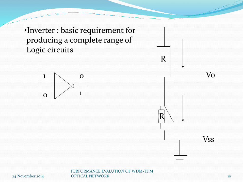
•Inverter : basic requirement forproducing a complete range ofLogic circuits

24 November 2014 11
Vdd
Vss
Vo
Vin
R Pull-Up
Pull Down
Basic Inverter: Transistor with sourceconnected to ground and a load resistorconnected from the drain to the positiveSupply rail
Output is taken from the drain and controlinput connected between gate and ground
Resistors are not easily formed in silicon- they occupy too much area
Transistors can be used as the pull-up device

24 November 2014 12
Vdd
Vss
Vo
Vin
D
S
D
S
• Pull-Up is always on – Vgs = 0; depletion
• Pull-Down turns on when Vin > Vt
NMOS Depletion Mode Transistor Pull - Up
VtV0Vdd
Vi
• With no current drawn from outputs, Idsfor both transistors is equal
Non-zero output
24 November 2014 13
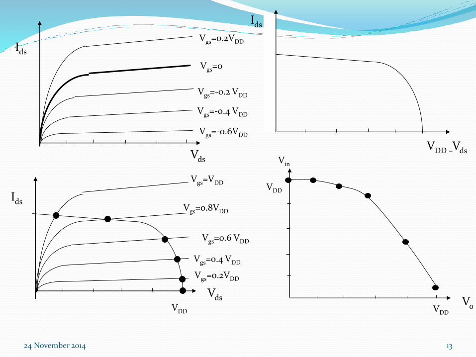
Vgs=0.2VDD
Vgs=0.4 VDD
Vgs=0.6 VDD
Vgs=0.8VDD
Vgs=VDD
Ids
Vds
VDD
VoVDD
VDD
Vin
Ids
VDD –Vds
Ids
Vds
Vgs=-0.6VDD
Vgs=-0.4 VDD
Vgs=-0.2 VDD
Vgs=0
Vgs=0.2VDD
24 November 2014 14
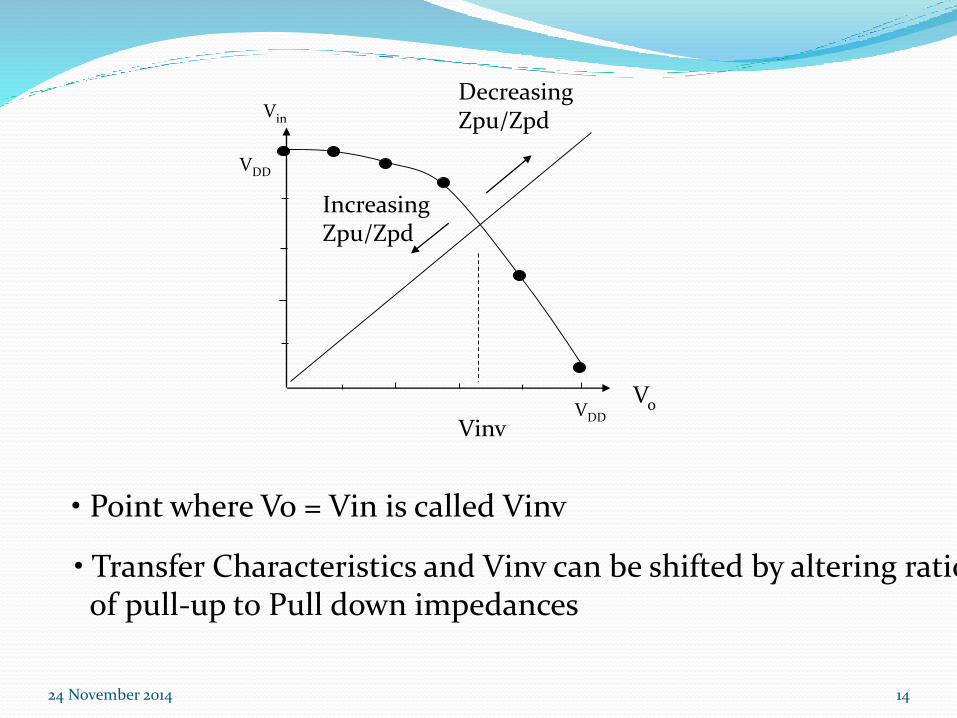
VoVDD
VDD
Vin
Vinv
• Point where Vo = Vin is called Vinv
DecreasingZpu/Zpd
IncreasingZpu/Zpd
• Transfer Characteristics and Vinv can be shifted by altering ratio of pull-up to Pull down impedances

24 November 2014PERFORMANCE EVALUTION OF WDM-TDM OPTICAL NETWORK 15
NMOS Depletion Mode Inverter Characteristics
Dissipation is high since rail to rail current flows when Vin = Logical 1
Switching of Output from 1 to 0 begins when Vin exceeds Vt of pull down device
When switching the output from 1 to 0, the pull up device is non-saturated initially and this presents a lower resistance through which to charge capacitors (Vds < Vgs – Vt)
24 November 2014 16
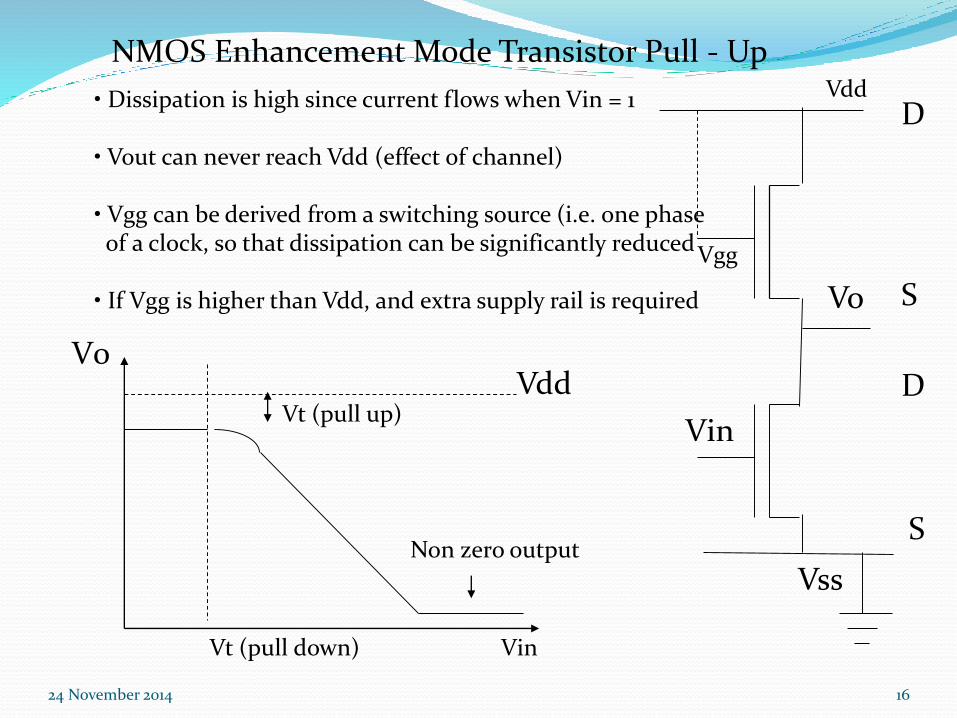
Vss
Vo
Vin
D
S
D
S
NMOS Enhancement Mode Transistor Pull - UpVdd
Vgg
Vt (pull down)
V0Vdd
Vt (pull up)
Non zero output
Vin
• Dissipation is high since current flows when Vin = 1
• Vout can never reach Vdd (effect of channel)
• Vgg can be derived from a switching source (i.e. one phaseof a clock, so that dissipation can be significantly reduced
• If Vgg is higher than Vdd, and extra supply rail is required
24 November 2014 17
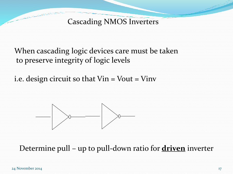
When cascading logic devices care must be takento preserve integrity of logic levels
i.e. design circuit so that Vin = Vout = Vinv
Cascading NMOS Inverters
Determine pull – up to pull-down ratio for driven inverter

24 November 2014 18
Assume equal margins around inverter; Vinv = 0.5 Vdd
Assume both transistors in saturation, therefore:Ids = K (W/L) (Vgs – Vt)2/2
Depletion mode transistor has gate connected to source, i.e. Vgs = 0
Ids = K (Wpu/Lpu) (-Vtd)2/2
Ids = K (Wpd/Lpd) (Vinv – Vt)2/2
Enhancement mode device Vgs = Vinv, therefore
Assume currents are equal through both channels (no current drawn by load)
(Wpd/Lpd) (Vinv – Vt)2 = (Wpu/Lpu) (-Vtd)2
Convention Z = L/W
Vinv = Vt – Vtd / (Zpu/Zpd)1/2
Substitute in typical values Vt = 0.2 Vdd ; Vtd = -0.6 Vdd ; Vinv = 0.5 Vdd
This gives Zpu / Zpd = 4:1 for an nmos inverter directly driven by another inverter
24 November 2014 19
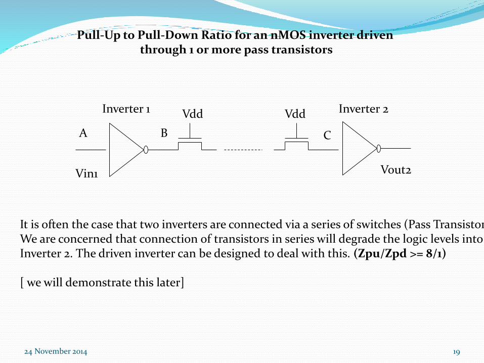
Vdd Vdd
A B C
Inverter 1 Inverter 2
Vin1 Vout2
Pull-Up to Pull-Down Ratio for an nMOS inverter driven through 1 or more pass transistors
It is often the case that two inverters are connected via a series of switches (Pass Transistors)We are concerned that connection of transistors in series will degrade the logic levels into Inverter 2. The driven inverter can be designed to deal with this. (Zpu/Zpd >= 8/1)
[ we will demonstrate this later]

CMOS Inverter
VDD
A Y
GNDA Y
CMOS Inverter
01
0
YA VDD
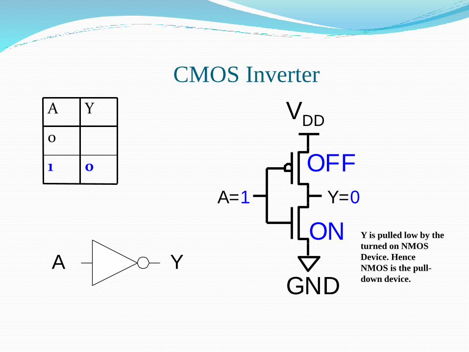
A=1 Y=0
GND
ON
OFF
A Y
Y is pulled low by the
turned on NMOS
Device. Hence
NMOS is the pull-
down device.

CMOS Inverter
01
10
YA VDD
A=0 Y=1
GND
OFF
ON
A Y
Y is pulled high by
the turned on PMOS
Device. Hence PMOS
is the pull-up device.

Complimentary Transistor Pull – Up (CMOS)
Vdd
Vss
VoVin
Vout
Vin
VddVss
Vtn Vtp
Logic 0 Logic 1
P onN off
Both On
N onP off

24 November 2014 24
Vout
Vin
VddVss
Vtn Vtp
P onN off
Both On
N onP off
1 2 3 4 5
1: Logic 0 : p on ; n off
5: Logic 1: p off ; n on
2: Vin > Vtn. Vdsn large – n in saturationVdsp small – p in resistiveSmall current from Vdd to Vss
4: same as 2 except reversed p and n
3: Both transistors are in saturationLarge instantaneous current flows

CMOS Inverter Characteristics
No current flow for either logical 1 or logical 0 inputs
Full logical 1 and 0 levels are presented at the output
For devices of similar dimensions the p – channel is slower than the n – channel device

26
Digital CMOS Logic
Circuits
24 November 2014 27
Introduction
CMOS is by far the most popular technology for the implementation of digital systems.
The small size, ease of fabrication, and low power dissipation of MOSFETs enable extremely high levels of integration of both logic and memory circuits.

DIGITAL CIRCUIT DESIGN
Digital IC Technologies and Logic-Circuit Families.
CMOS: CMOS technology is, by a large margin, the
most dominant of al the IC technologies available for
digital-circuit design.
These are a number of reasons for this development,
the most important of which is the much lower power
dissipation of CMOS circuits.

24 November 2014 29
Digital IC technologies and logic-circuit families.
24 November 2014 30
COMPARISION
Some of the reasons for CMOS displacing bipolar technology in digital applications are as follows:
1.CMOS logic circuits dissipate much less power than bipolar logic circuits and thus one can pack more CMOS circuits on a chop than is possible with bipolar circuits.
2.The high input impedance of the MOS transistor allows the designer to use charge storage as a means for the temporary storage of information in both logic and memory circuits.

24 November 2014 31
3.The feature size(i.e., minimum channel length) of the MOS transistor has decreased dramatically over the years. This permits very tight circuit packing and, correspondingly, very high levels of integration.
CMOS circuits based on the inverter are the most widely used.
Bipolar: Two logic-circuit families based on the bipolar junction transistor are in some use at present: TTL and ECL.

24 November 2014 32
BiCMOS: BiCMOS combines the high operating speeds
possible with BJTs( because of their inherently higher
transconductance ) with the low power dissipation and
other excellent characteristics of CMOS. At present,
BiCMOS is used to great advantage in special applications,
including memory chips.
Gallium Arsenide (GaAs): The high carrier mobility in
GaAs results in very high speeds.

24 November 2014 33
BABAY
The Two-Input NOR Gate
A two-input CMOS NOR gate.
24 November 2014 34
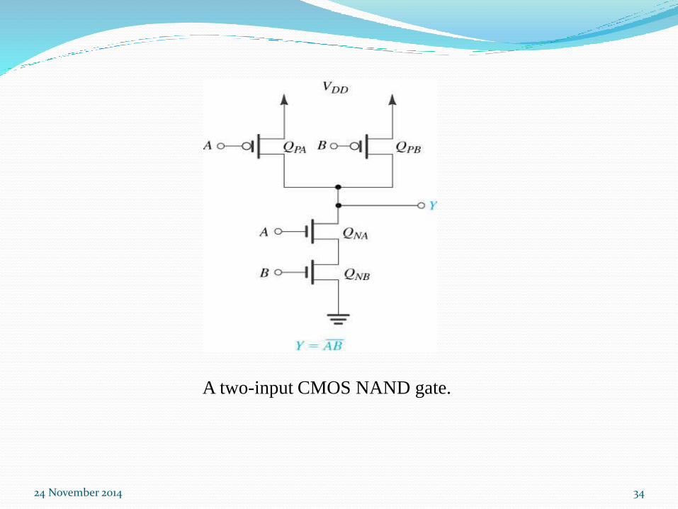
A two-input CMOS NAND gate.

24 November 2014
THANK YOU
35