Embed Size (px)
Citation preview

VLBA Technical Report No. 38VLBA 5 MHZ Distributor
Module L121Alan E.E. Rogers
October 1988

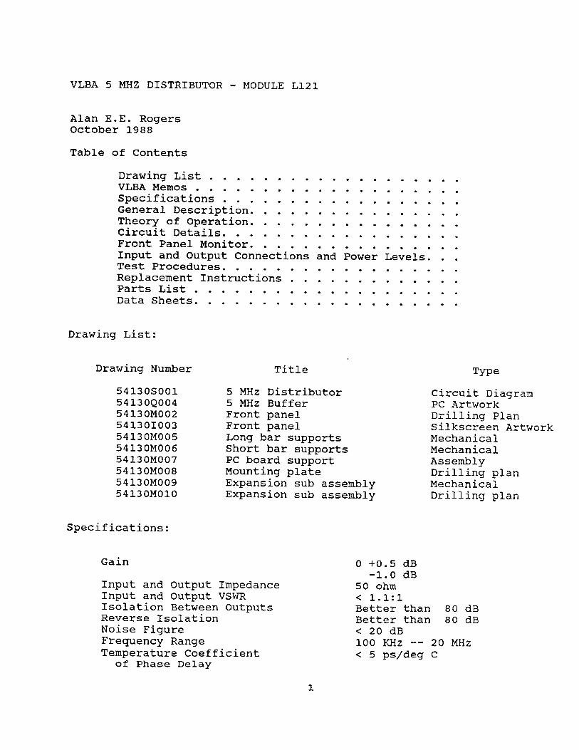
VLBA 5 MHZ DISTRIBUTOR - MODULE L121
Alan E.E. Rogers October 1988Table of Contents
Drawing List .....................................VLBA Memos .......................................Specifications ...................................General Description..............................Theory of Operation..............................Circuit Details...................................Front Panel Monitor..............................Input and Output Connections and Power Levels. .Test Procedures...................................Replacement Instructions ........................Parts List .......................................Data Sheets.......................................
Drawing List:
Drawing Number54130S001 54130Q004 54130M002 541301003 54130M005 54130M006 54130M007 54130M008 54130M009 54130M010
Title5 MHz Distributor5 MHz Buffer Front panel Front panel Long bar supports Short bar supports PC board support Mounting plate Expansion sub assembly Expansion sub assembly
TypeCircuit Diagram PC Artwork Drilling Plan Silkscreen Artwork Mechanical Mechanical Assembly Drilling plan Mechanical Drilling plan
Specifications:
GainInput and Output Impedance Input and Output VSWR Isolation Between Outputs Reverse Isolation Noise Figure Frequency Range Temperature Coefficient
of Phase Delay
0 +0.5 dB -1.0 dB
50 ohm < 1 . 1:1Better than 8 0 d3 Better than 8 0 dB< 20 dB100 KHz — 20 MHz< 5 ps/deg C
1
Nominal Pulse Delay Nominal Input Level Harmonic Distortion
5 ns + 13 dBm - 40 dBc
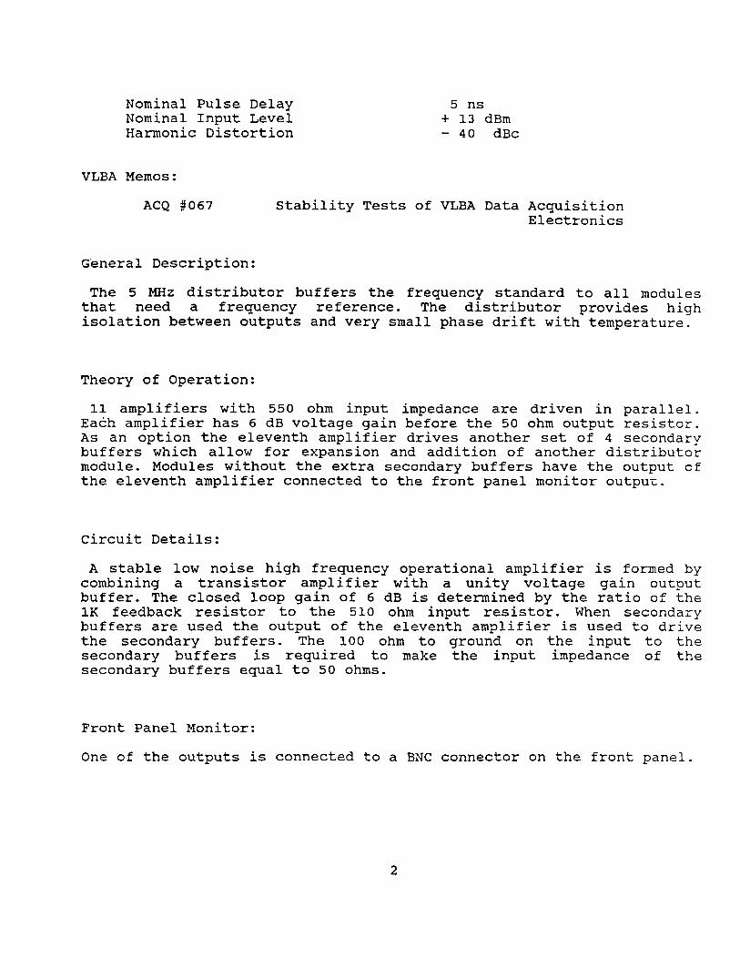
VLBA Memos:ACQ #067 Stability Tests of VLBA Data Acquisition
Electronics
General Description:The 5 MHz distributor buffers the frequency standard to all modules
that need a frequency reference. The distributor provides high isolation between outputs and very small phase drift with temperature.
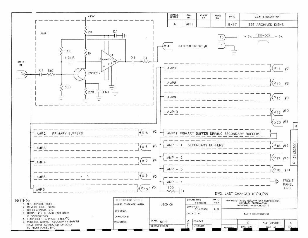
Theory of Operation:11 amplifiers with 550 ohm input impedance are driven in parallel.
Each amplifier has 6 dB voltage gain before the 50 ohm output resistor. As an option the eleventh amplifier drives another set of 4 secondary buffers which allow for expansion and addition of another distributor module. Modules without the extra secondary buffers have the output cf the eleventh amplifier connected to the front panel monitor output.
Circuit Details:A stable low noise high frequency operational amplifier is formed by combining a transistor amplifier with a unity voltage gain output buffer. The closed loop gain of 6 dB is determined by the ratio of the IK feedback resistor to the 510 ohm input resistor. When secondary buffers are used the output of the eleventh amplifier is used to drive the secondary buffers. The 100 ohm to ground on the input to the secondary buffers is required to make the input impedance of the secondary buffers equal to 50 ohms.
Front Panel Monitor:One of the outputs is connected to a BNC connector on the front panel.
2
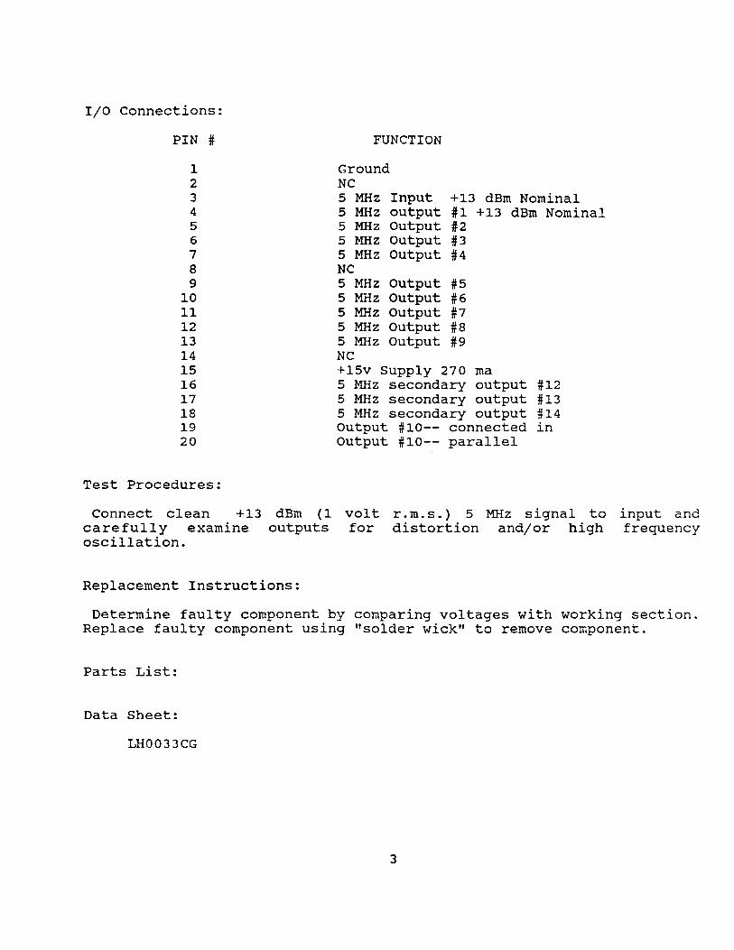
I/O Connections:PIN # FUNCTION
1 Ground2 NC3 5 MHz Input +13 dBm Nominal4 5 MHz output #1 +13 dBm Nominal5 5 MHz Output #26 5 MHz Output #37 5 MHz Output #48 NC9 5 MHz Output #5
10 5 MHz Output #611 5 MHz Output #712 5 MHz Output #813 5 MHz Output #914 NC15 +15v Supply 270 ma16 5 MHz secondary output #1217 5 MHz secondary output #1318 5 MHz secondary output #1419 Output #10— connected in20 Output #10— parallel
Test Procedures:Connect clean +13 dBm (1 volt r.m.s.) 5 MHz signal to input and
carefully examine outputs for distortion and/or high frequency oscillation.
Replacement Instructions:Determine faulty component by comparing voltages with working section.
Replace faulty component using "solder wick" to remove component.
Parts List:
Data Sheet:LH003 3CG
3
+ 1 5 V .CHANGELETTER
OWNB Y
C H K ’OBY
A P P ’OBY
DATE D.C .N . 4 DESCRIPTION
r 1I 1 A APH 9 /8 7 SEE ARCHIVED DISKS
5MHzIN
AMP 1
■01 510 H l— v w
1.1K <J IK
4.7p.F. I I
5
I I
2N2857
rAMP2 PRIMARY BUFFERS
rUAM P4
ruAMP 5
rL_AMP 6
NOTES:1. N T . APPROX. 20dD2. REVERSE ISO L. 9 0 d fl 3 D E LAY A PPRO X. 5nS4. OUTPUT # 1 0 IS USED FO R DOTH
IF DISTRIBUTORS5. TEMP COEFF. APPROX. + 3 p s / ° C6 . VERSIONS W ITHO UT S E C O N D A R Y BUFFER
H A V E AMP1I CONNECTED D IR E C TLYTO FRONT P A N E L QNC
AMP8
BUFFERED OUTPUT #1
QD-D >
+ 15V. 1250-003 +15v
/---\
nL_AMP7_________________ j-O 11 #7
“1|\ ° 12 #8
j----------------------------------------------------------------------------------------------------------------
j_ A LP?_____________________________________________________ f\° 13 ft 9
AMP10
j_AMP11 PRIMARY BUFFER DRIVING SECONDARY BUFFERS
n0 19 #10
o 20 #11
~ 1 _ o 7 iH
k- i~i
10
ft 5
tf&
AMP - 1 SECONDARY BUFFERS
_I 1_______________________ |\°17 #13
__| \ ° 16 § 12
rU AMP - 3
r
oo</>0rOm1o
L_‘AMP
|~V° 1 8 #14 ~l
100
1__ (o FRONTI V PANEL
BNC
DWG. LAST CHANGED 1 0 /3 1 /8 8
ELECTRONIC NOTES:
UNLESS OTHERWISE NOTED:
RESISTORS:
C APACITORS:
INDUCTORS:
U S E D ON
DRAWN FOR:
A E ROGERS
DRAWN BY:A PHIL BROOK
CHECKED BY:
DATE:
7 - 8 7NORTHEAST RADIO OBSERVATORY CORPORATION
HAYSTACK OBSERVATORY WESTFORO, M ASSACHUSETTS
5 M H z D IS TR IB U TO R
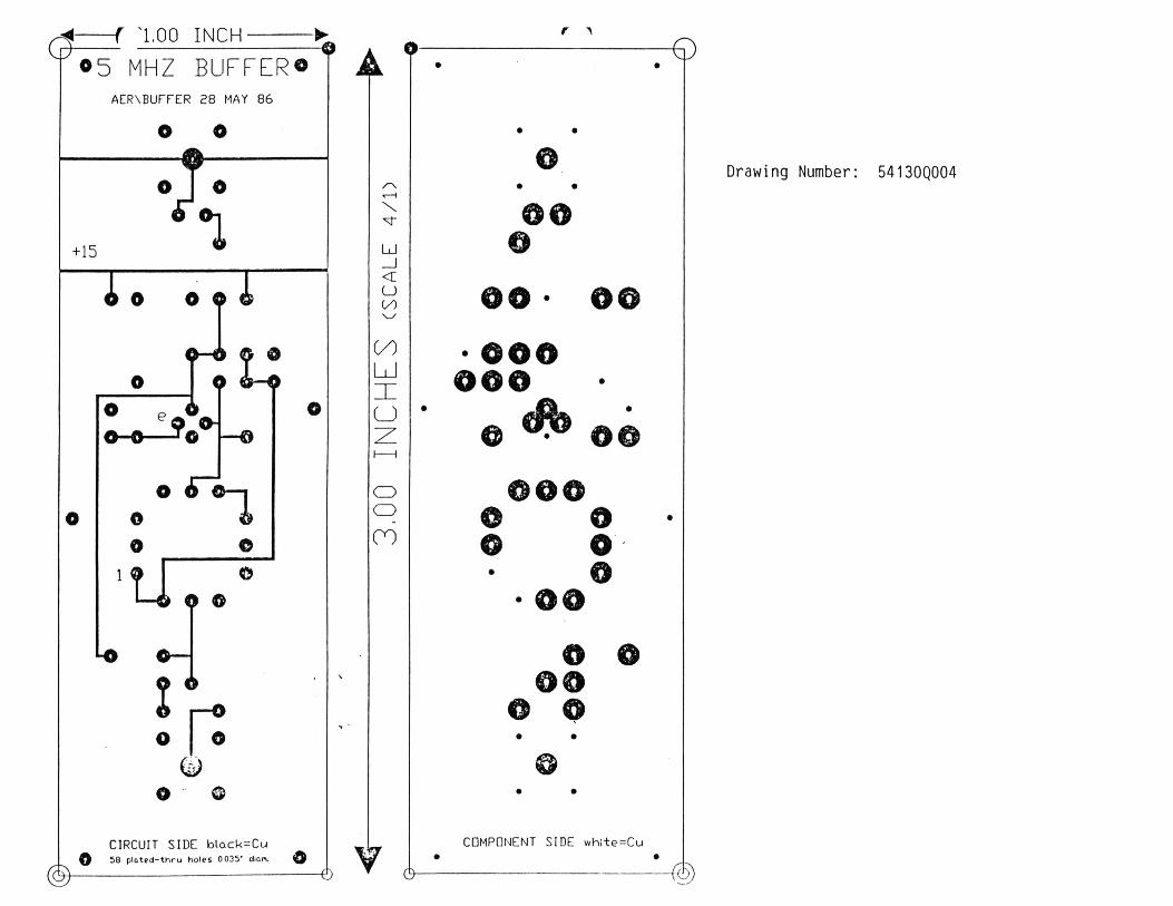
-f '1.00 INCH
0 5 M H Z B U F F E R ®AERXBUFFER 28 MAY 86
© o
o o
+ 15 11o 0 0
o
— a
o dTi
$
oo
* 1e
1 ^ oL— © ©
r:O
o ' o
CIRCUIT SIDE b tack = CuQ 5 8 p lo te d - t t i r u ho les 0 0 3 5 ' diort. Q
• i1
\r
LJ_1CCJ00w
(7 )L dIUZ1---1
CDCD
\
0 0
*»
07
&
©
• •
• •
COMPONENT SIDE white=Cu
Drawing Number 54130Q004
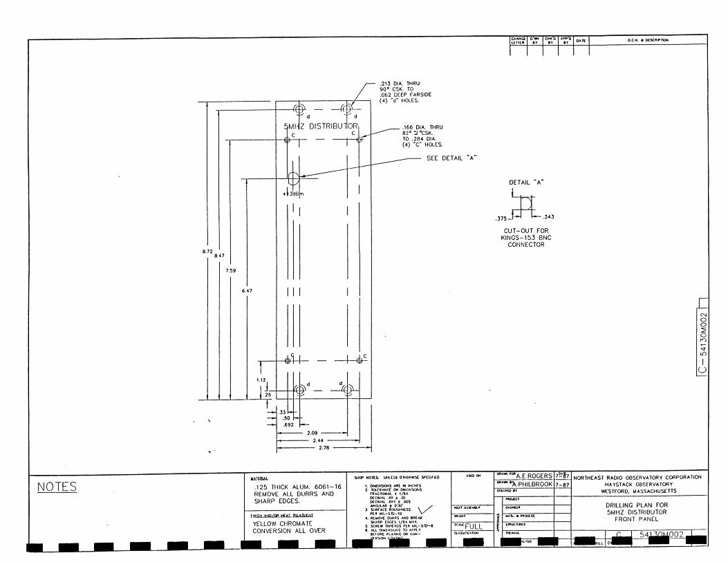
CHK'O o c n . k ocsch ip tkin
.2 1 3 DIA. THRU 9 0 * CSK. TO .0 6 2 DEEP FARSIDE: ( 4 ) "d " HOLES.
.1 6 6 D IA . THRU 82 o 2 °CSK.TO .2 8 4 DIA. (4 ) ’ C " HOLES.
SEE D E TA IL "A
D E TA IL " A ”
.3 7 5 s .3 4 3
C U T -O U T FOR K IN G S -1 5 J B NC
C O N N E C TO R
NOTES .1 2 5 THICK ALU M . 6 0 6 1 - T 6 REM O VE ALL D U R R S AND S H A R P EDGES.
I 'WICH AMD/Oft HfAT TRLATMENT
YELLOW CHROMATE CONVERSION ALL OVER
SHOP NOTES: UNI ESS OTHERWISE SPECiriEO
1. OIUCNSJONS ARC IN INCHES2. TOLERANCE ON DIMENSIONS
FRACTIONAL t 1/fl4 DECIMAL .XX i Of DECIMAL .XXX i 003 ANGULAR ± OMO* /
3. SURFACE ROUGHNESS \ /PER M ll-STD-10
4. REMOVE 3URRS AND BREAK SHARP EOCES 1/64 MAX.
5. SCREW TMEAOS PEN MIL-STI>-*6. A IL DIMENSIONS TO APPLY
BEfOKC PLATING OR CON -CRSlON
U M m m
NCXT AiMMHV
"A .E .R O G E R S
•X .P H IL B R O O K
7°-*&7
7 - 8 7
NORTHEAST R ADIO OBSERVATORY CORPORATION HAYS TA C K OBSERVATORY
WESTFORO, M ASSACHUSETTS
D R ILLIN G PLA N FOR 5 M H Z D IS TR IB U TO R
FR O N T P A N E L
C~
5413
0M00
2 n

i
2.78 (REF.)
8.72 (REF.)
(6 ) (O)5MHZ
DISTRIBUTOR5MHZ
DISTRIBUTOR
© ©
0-*-13dBn +13dBm
© ©
L121(O) (O)
L121
SILK SCREENED PANEL ARTVDRK
1 ! a -3»si
■ O U N - Z
2 t j O
t ) <j » ^ m m ^ > z-i °Z ‘’ I H Ie§>5o?ig>>|§.ss•“ 3 ? z
i/ i r-
BL^ c ^ - - oS? qS"1^ » o-"3
» -5413 0 1 0 0 3
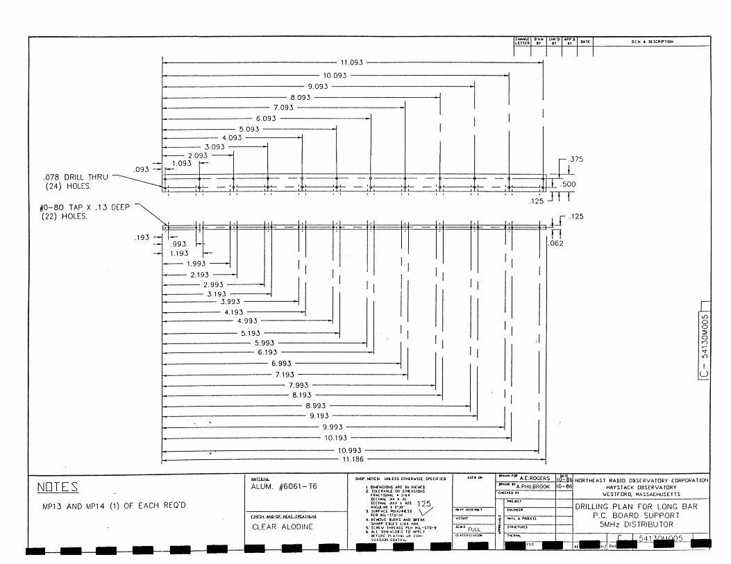
— .375
.078 DRILL THRU (24) HOLES.
# 0 -80 TAP X .13 DEEP (22) HOLES. .125
O C R 1 DC SCRIPT ION
n
t f e lU io L
ALUM. #6061 -T 6SHOP N O Kfc I f * ESS OIHCRVISC SPC C iriCD
1. d im ensions ARC In Ire n e s2. IO lCRanCC Oh DIMENSIONS
FRAC • I0NAI t J/fc4 DCClMAl .XX * .01 DC Cl HAL .XXX t 005 1 9 ^ AN&ULAR t O’ JO' ' /
3. SURTACC RtluG^rCSS \ /PCR M lL-STD-lO v '
4. R C O v C luR RS AND BREAK SHARP CDOfS 1/64 MAX
3. S C R IV THREADS P tK H Il-S T D -9 6. A l l D lHlNSIO iS 10 APPL r herOPf P lA flN G UR CONVERSION COAT |(« i
USC1 UN
NEXT ASSCHbLV
TIN IIM ANQ/QP HCAI T P Q IH L N I
CLEAR ALODINEWC1GHT
XC" C FULLCLAssincAiioN
NOTES
MP13 AND MP14 (1) OF EACH REQ'D
A.E.ROGERS
A PHILBROOK
HM l fc fKO CtII
NO RTHEAST R AD IO O B S E R V A TO R Y CORPORATION H A Y S TA C K O B S E R V A TO R Y
V E S T fD R D , M ASSACHUSETTS
DRILLING PLAN FOR LONG BAR P.C. BOARD SUPPORT
5MHz DISTRIBUTOR
IES____ BE
CHANGELE T T E R
OWNBY
CHK'DBY
APP'DBY DC.N. I DESCRIPTION
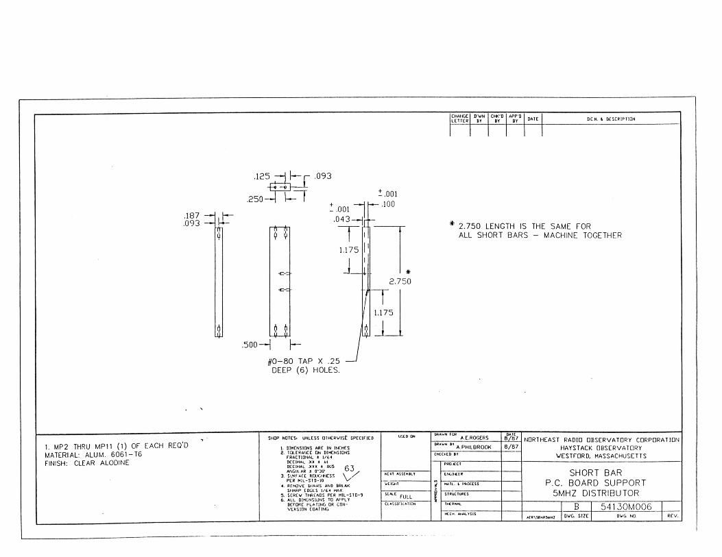
•i25 ± ^ r- p t— ■1
.2 5 0 - H U T
.093
.187.093
.500
i*i fr <• V
i) iji -1* 1___
# 0 -8 0 TAP X .25 DEEP (6 ) HOLES.
2.750 LENGTH IS THE SAME FORALL SHORT BARS - MACHINE TOGETHER
1. MP2 THRU MP11 (1) OF EACH REQ’D
MATERIAL: ALUM. 6061-T6
FINISH: CLEAR ALODINE
SHOP NOTES. UNLESS O TM ERV lS t SPE C IF IE D
63
I . DIMENSIONS ARE IN INCHESZ TDLERANCE ON DIMENSIONS f r a c t i o n a l t 1/64 DECIMAL XX l .01 DECIMAL .XXX t 005 ANGULAR J O'JO'
3. SCKI ACE ROUGHNESS PER M IL-STD -IO
4. RfMOVE LUkKS AND BRLAK SHARP CDGLS l/fc« MAX.
3. SCREW THREADS PER M IL-STD -96. A LL DIMENSIONS TO APPLY
BE r ORE P L A TINCi OR CONVERSION COATING.
NCXI ASSCMILT
CLASSIFICATION
A P H ILB R O O KCHCCkED I t
MAIL. I PROCESS
ML C H AUALTSIS
date8 / B 7
8 / 8 7N O R TH E A S T R A D IO O B S E R V A T O R Y C O R P O R A T IO N
H A Y S T A C K O B S E R V A T O R Y
V E S T F O R D , M A S S A C H U S E T T S
SHORT BAR P.C. BOARD SUPPORT
5MHZ DISTRIBUTOR
Af R\S0aN5mhZ
54130M006
0 C N. k OCSCRlPnOH
MPT ‘
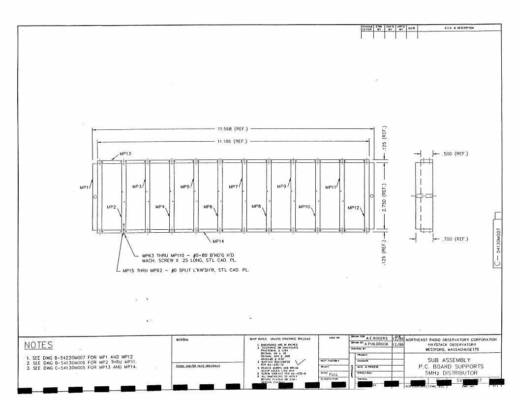
11.568 (REF.)
11.186 (REF.)
MP13
MP2
MP31
MP4
MP51
MP6
MP7 1
MP8
MP9 ■
MP10
\
MP1,/
MP12 \± L
H h - .500 (REF.)
_ Lr
MP14
MP63 THRU MP110 - #0-60 B’ND’G H’D MACH. SCREW X .25 LONG, ST'L CAD. PL.
MP15 THRU MP62 - H0 SPLIT L'KW'SH'R. ST’L CAD. PL.
J .700 (REF.)
c
NOTES
1. SEE DWG B-54220M007 FOR MP1 AND MP122. SEE DWG 0-5413GM006 FOR MP2 THRU MP11.3. SEE DWG C—541 30M005 FOR MP13 AND MP14.
SHCf* NOTtS: UNLESS OTHtRwiSC SPECflEO
1. DIMENSIONS ARC IN INCHES2. TOlERANCC ON CrfMlNSiUNS
fra c t io n a l t 1/ 6*DECIMAL XX 1 .01 DECIMAL .XXX ± .005 ANGl»LAR ± 0 30'
J SURFACE ROUGHNESS PER MiL-STD-10
4. REMOVE BURRS ANO BREAK SHARP EDGES 1/64 MAX
5 SCREW THREADS Pf.K mil-S T D -9 8. ALL DIMENSIONS TO APPLY
BfFOK'E Pi A UN C ON CON- VtRSlON CGAtuu — m
\S NC*T ASSCUiLY
aASuncAnoN
AE.R O G E R Sora™ by ApHIL0RoOK
ha iv. * w o a s s
tf/%612/86
NORTHEAST RADIO O BSERVATORY CORPORATION HAYSTAC K O BSERVATORY
WESTFORD. MASSACHUSETTS
SUB ASSEMBLY P.C. BOARD SUPPORTS
5MHz DISTRIBUTOR
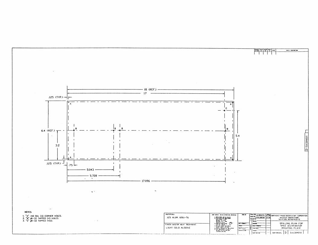
NOTES.
1. *A " .140 DIA. (4 ) CORNER HOLES.2. 'B ' / 6 - J 2 TAPPED ( 4 ) HOLES i . " C # 8 -3 2 ta p p e d h o le
HATCRIAL.
125 ALUM 6061-T6
riN ISM AIJD/n# K A I TfiEATMf NTi
LIG HT GDLD ALODINE
tO RTH CA lT »ADIO D I U I V « T U . l C C»lMJ<fAt 10*w n n t ic o m a v A to 'r v u i r o « n «AiiAC>uiCTitDR ILLIN G PLAN fD R 5MH? DIS TRI BUT UR MOUNTING PLA1E
Ai«\3t.«;n. D 5-4I30M00A
[D-5
4130
*00°
CHANGELE TTE R
CHK'Dbv DC.N. t DESCRIPTION
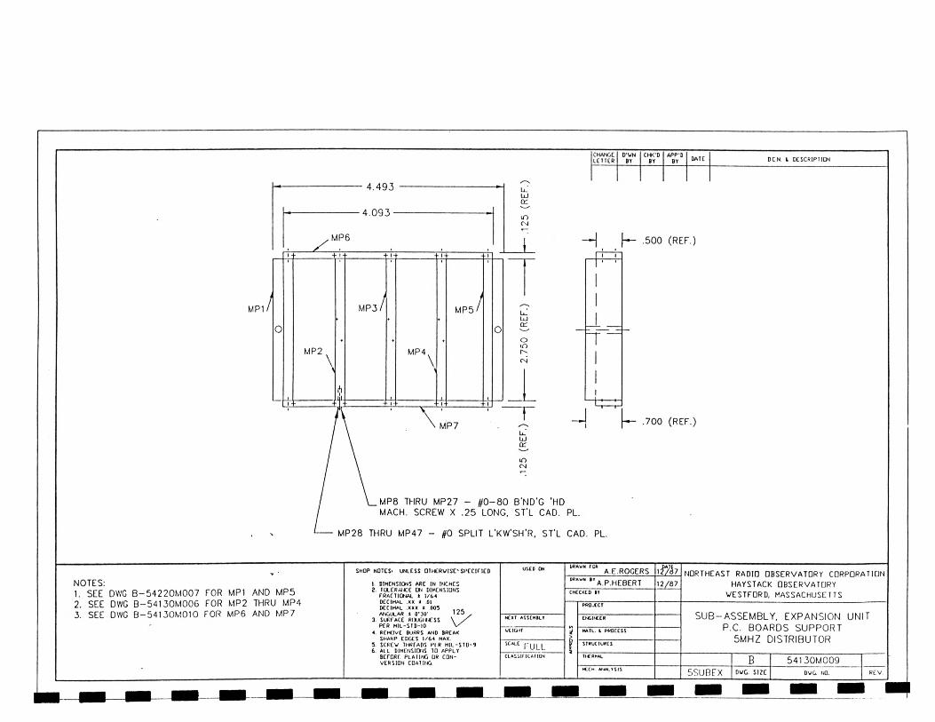
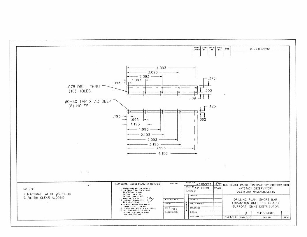
NOTES:
1. MATERIAL: ALUM. #6061-T6
2. FINISH: CLEAR ALODINE
SHOP NOTES. UNLESS O TH ER W ISC 'SP EC IflED
I. DIMENSIONS ARC IN INCHES Z. TOLERANCE ON DIMENSIONS FRACTIONAL * 1/64 DCCImal XX t 01 DECIMAL .XXX t .005 ANGULAR 1 0*30' 1 2 5
3. SURrACE ROUGHNESS PCR M IL-S ID -10
4. R EM O VE U lJk kS AMD B R EA K SH A RP IU G C S 1/64 MAX.
5. SCRCV IHREADS PER M ll-S T D - G. A IL DIMENSIONS TO APPLY
BCrORE P lA I I t iG UR CONVERSION COATING.
N O T ASSCM HT
FULLCLASSiriCAHON
A.E.ROGERSA.P.HEBERT
m a il , i p r o c e s s
MIC1 2 /8 7
1 2 /8 7N O R TH E A S T R A D IO O B S E R V A T O R Y C O R P O R A T IO N
H A Y S TA C K O B S E R V A T O R Y
V E S T F O R D , M A S S A C H U S E TTS
DRILLING PLAN, SHORT BAR
EXPANSION UNIT, P C. BOARD SUPPORT. 5MHZ DISTRIBUTOR
5MHZCXB 541 J0M010
DUO. NU.

Page No. 111/25/88
PARTS LIST FROM DBASE FILE:PARTS.DBFREF SUBMOD PART DESC MFR COST QTY TOTAL COST
MP1 5M 1009-1511-000 SMC PC CONN AEP 2.25 12 27.00C03 5M 103K 0.01 UF AVX 0.10 11 1.10C01 5M 104K 0.1 UF AVX 0.10 33 3.30MP 5M 1105-7521-003 SMC CABLE PLUG AEP 2.49 15 37.35MP2 5M 1250-003 FEED THRU ERIE 1.53 1 1.53MPX 5M 200458-1 BLOCK AMP 3.00 1 3.00MPX 5M 200833-4 GUIDE PINS AMP 0.36 0.72MPX 5M 200835-4 GUIDE SOCKETS AMP 0.48 0.96MPX 5M 201142-2 SPRING AM? 0.05 11 0.55MPX 5M 201143-5 COAXICON PIN AMP 2.70 11 29.70MPX 5M 202394-2 HOOD AMP 1.04 1 1.04MPX 5M 202422-1 POWER PINS AMP 0.50 4 2.00Q01 5M 2N2857 2N2857 MOTOROLA 0.81 11 8.91MPX 5M 328666 FERRULE AMP 0.08 11 0.88C02 5M 4R7J 4.7 PF AVX 0.50 11 5.50SS 5M 541301003 F.P.SILK SCREEN NYES 100.00 1 100.00MS 5M 54130M002 FRONT PANEL HAYSTACK 100.00 1 100.00MS 5M 54130M007 PC BOARD SUPPORT HAYSTACK 100.00 1 100.00MS 5M 54130M008 CENTER PLATE HAYSTACK 20.00 1 20.00MPX 5M 5807-1501-000 SMC TEE AEP 12.70 1 12.70PC 5M AER\BUFFER PC BOARD PACLAB 40.00 11 440.00MS 5M C53306M013-2UA FRONT PANEL PREC.MACHINE 20.00 1 20.00MS 5M C53306M014-2UA PERFORATED COVER PREC.MACHINE 10.00 20.00MS 5M C53306M015-2UA MODULEREAR PANEL PREC.MACHINE 20.00 1 20.00MS 5M C53306M016 BAR SUPPORT PREC.MACHINE 10.00 4 40.00MS 5M C53306M017 SIDE PLATE PREC.MACHINE 10.00 20.00WORK 5M ENGINEER CHECKOUT HAYSTACK 100.00 1 100.00MP19 5M KC19-153 F.P.BNC KINGS 6.76 1 6.76U001 5M LH0033CG LH0033 ANALOG DEV 22.00 11 242.00R02 5M RCR05G112J 1.1K OHM 1/8W AB 0.20 22 4.40R03 5M RCR05G200J 20 OHM 1/8W AB 0.20 11 2.20R05 5M RCR05G271J 270 OHM 1/8W AB 0.20 11 2.20R04 5M RCR05G510J 51 OHM 1/8W AB 0.20 11 2.20R01 5M RCR05G511J 510 OHM 1/8W AB 0.20 11 2.20R06 5M RCR05G561J 560 OHM 1/8W AB 0.20 11 2.20WORK 5M TECH ASSEMBLY WORK HAYSTACK 10.00 24 240.00
Total ***1620.40
ANALOG DEVICES
FEATURES2nd Source—Replaces All LH0033G SeriesWide Bandwidth—dc to 100MHzHigh Slew Rate—1500V/puOperates on Single or Dual Power SuppliesOperation Guaranteed -55° C to +125°C (ADLH0033G)High 10“ f t Input Impedance
APPLICATIONS High-Speed Line Drivers Video Impedance Transformation High-Speed A /D Input Buffers Nuclear Instrumentation Amplifiers Coaxial Cable Drive
GENERAL DESCRIPTIONThe ADLH0033G and ADLH0033CG arc supcrhigh speed (1500VY/js slew rate) and high input Impedance (1 0 l l ft) buffer amplifiers, designed to replace all LH003 3 series amplifiers in applications such as high-speed line drivers or as high impedance buffers for fast A /D converters and com parators.The ADLH003 3G and ADLH0033CG arc rated for operation over the voltage range of ±5V to ±20V. The ADLH0033G is guaranteed over the tem perature range o f -55°C to +125°C, while the commercial grade ADLH003 3CG is guaranteed over the range o f -25°C to +85°C.Guaranteed operation over tem perature o f the ADLH0033G is achieved by using specially, selected junction FET’s and the latest state-of-the-art laser trim ming techniques. They are available in the industry standard 12 pin TO-8 metal can.OPERATION WITHIN AN OP AMP LOOP When using the ADLH0033G/ADLH0033CG as a current booster or isolation buffer with op amps such as LH0032, 118, 741, etc., an isolation resistor of at least 47 ft m ust be
Figure 1. Offset Adjustment
High Speed Buffer Amplifiers
ADLH0033G/ADLH0033CGADLH0033G/ADLH0033CG
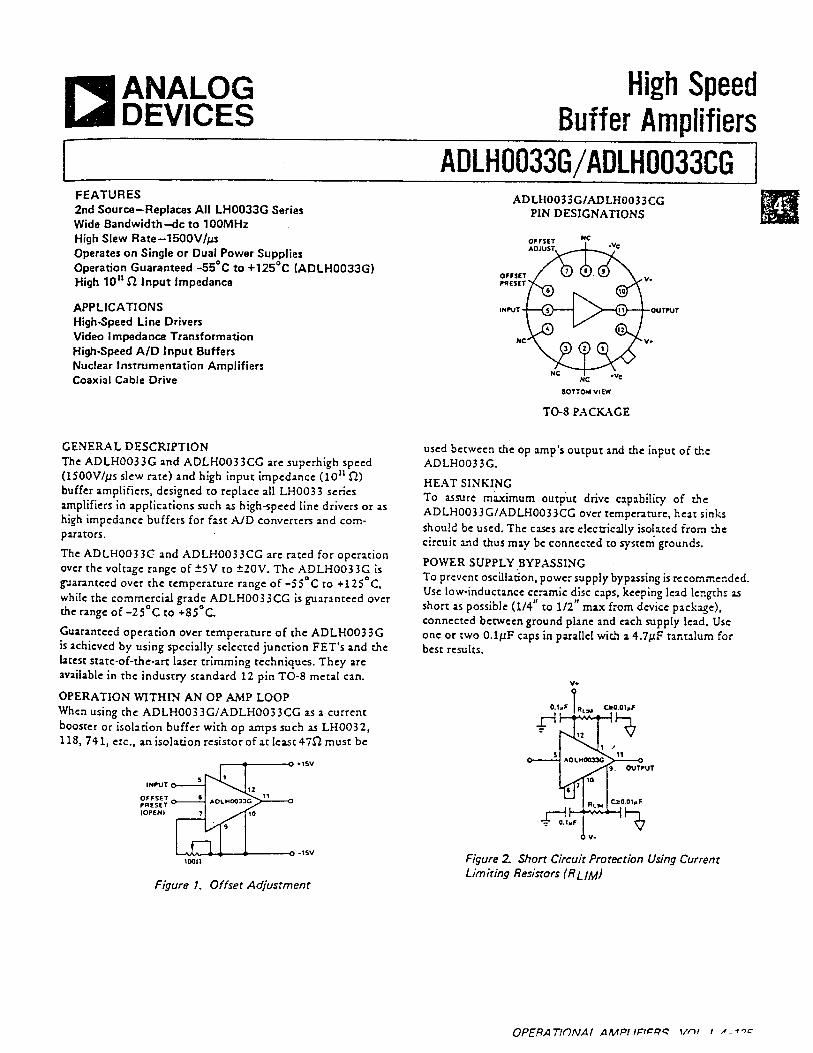
PIN DESIGNATIONS
TO-8 PACKAGE
used between the op am p’s output and the input o f the ADLH0033G.HEAT SINKINGTo assure maximum output drive capability of the ADLH0033G/ADLH0033CG over temperature, heat sinks should be used. The cases arc electrically isolated from the circuit and thus may be connected to system grounds.POWER SUPPLY BYPASSINGTo prevent oscillation, power supply bypassing is recommended. Use low-inductance ceramic disc caps, keeping lead lengths as short as possible (1/4* to 1/2” max from device package), connected between ground plane and each supply lead. Use one or two 0.1/iF caps in parallel with a 4.7/iF tantalum for best results.
v*
Figure 2. Short Circuit Protection Using Current Limiting Resistors (Ru m )
OPERATION A t AM PIIR f^Q ^ \ /n i /

SPECIFICATIONSA n t . i io n n c c
A B S O LU TE M A X IM U M RATINGS Supp ly Voltage ( V * - V -)M axim um Power D issipation (see curves) M axim um Junc tion Temperature In p u t VoltageC ontinuous O u tp u t Current Peak O u tp u t C urren t O perating Tem perature AD LH 00J3G
ADLIIOO) )C G Storage Tem perature Range
4 0 V l.S W 175*CEqual to Supplies 1 100m A 1 250m A-S 5 *C to ♦ 1 2 5*C - 2 5*C to «85*C -6 5 *C to ♦1 5 0 *C )0 0 *C
A D LH 003 3G A D I.1100) )C C
Parameter C ond itions in in typ max nun typ m ax U n its
DC E L E C T R IC A L C H A R A C tE R IS T IC S 1- ’
In p u t B ia l C urrent T f 25*C 0.1 0.15 0.15 n A10 5 nA
In p u t Impedance R, • i k n IO 10 1 0 " IO 1* 1 0 " n
Voltage Gain V r I V tins , f * I k l l i , 0 .96 0 98 1.0 0 96 0 98 1.0 V /V
R, . i k n , r , - lo o v nO u tp u t O ffset Voltage ■ v lO O kU , Tc ■ 25"C J 10 12 20 m V
R, • io o k n 15 25 m V
O u tp u t O ffset V o ltage TC R , . lOOkQ 50 100 50 100 j iV / * C
O u tp u t Impedance V ,N - IV m i , 1 • l k H t 6 10 6 10 n
Rs • io o k n , r l ■ u nO u tp u t Voltage Swing R| • u n 112 11) 112 1 1 ) V
R, . 1 0 0 n ,T c - 2 $ ‘ C 19 19 V
vs- i s v . r l « u n 6 6 V p p
S upp ly Current
Power Consum ption
V1MV j .
vwV s *
■ OV. V j - l l S V 15VOV, Vs - 115V
15V
2011600180
25
660
21186 )0180
25
720
m A m A mW mW
Slew Rate B andw idth Phase N on linea rity Rise Tim e Propagation Delay H arm on ic D is to rtio n
V ^ - n O V V|N » IV rm i BW • 1 to 20M Hz A V ,* . 0 .5 V
. 0.5 V f > lk l l s
1000 150010022.91.2<0.1
1 '
1000 1400 100 2 ) 2 1.5 <0 .1
V /psM i l lDegreesnsns%
M TBFM eantim e Between Failure 1.962X 10 ’ hours
PAC KAG E O PTIO N* 111 2A I I 12 A
N O TES* U n lcu oiherwite ipecified, theM ipp ly for • I J V applied lo pln l 1 and I I . - I J V
applied lo puii 9 and 10, and pin 6 conneclcj io pin 7.1 U n lcu o lh irw iu noted, apecificttioni apply over a temperature range, - J 5 C < T ( ;< * I J S C
lor (he ADLMOOJ JG, and -2 J*C < T C <*»J C (or ihe AD I. Hoot )C G . Typical valuea ahown are lor T c • J J‘ C.
'See Section 19 for package outline Information.
Spccificanooa Subject to change m i i Iioui notice.
O R D E R IN G IN F O R M A T IO N
M u ilc t A D I IIOOJJCG A D I.1 100) )G
Tem pera tu re Range -2 5 *C to «85*C - 5 J * C to ♦ I2 5 ° C *»
UT#
OU
Trvn
VO
LTA
CC
Typical Performance Curves
Wft -+o
Power Dissipation vs TemperatureIn p u t Bus Current vs Temperature Rise and F a ll Tim e vs Tem perature
1- * t • HO
*1 • lOOhO lc - ‘ tt'c / /
/
/1
Supply Current vs Supply Voltage
«L»»IY vo irAG i _ IV
O utput Voltage vs Supply Voltage O utput Offset Voltage vs Tem perature
Negative Pulse Response Frequency Response