Embed Size (px)
Citation preview
Virtuoso AMS Designer Simulator Tutorials
Product Version 8.2November 2008
2007–2008 Cadence Design Systems, Inc. All rights reserved.Portions © Regents of the University of California, Sun Microsystems, Inc., Scriptics Corporation. Used bypermission.Printed in the United States of America.
Cadence Design Systems, Inc. (Cadence), 2655 Seely Ave., San Jose, CA 95134, USA.
The AMS Designer simulator contains technology licensed from, and copyrighted by: Regents of theUniversity of California, Sun Microsystems, Inc., Scriptics Corporation, and other parties and is © 1989-1994 Regents of the University of California, 1984, the Australian National University, 1990-1999 ScripticsCorporation, and other parties. All rights reserved.
Open SystemC, Open SystemC Initiative, OSCI, SystemC, and SystemC Initiative are trademarks orregistered trademarks of Open SystemC Initiative, Inc. in the United States and other countries and areused with permission.
MMSIM contains technology licensed from, and copyrighted by: C. L. Lawson, R. J. Hanson, D. Kincaid,and F. T. Krogh © 1979, J. J. Dongarra, J. Du Croz, S. Hammarling, and R. J. Hanson © 1988, J. J.Dongarra, J. Du Croz, I. S. Duff, and S. Hammarling © 1990; University of Tennessee, Knoxville, TN andOak Ridge National Laboratory, Oak Ridge, TN © 1992-1996; Brian Paul © 1999-2003; M. G. Johnson,Brisbane, Queensland, Australia © 1994; Kenneth S. Kundert and the University of California, 1111 FranklinSt., Oakland, CA 94607-5200 © 1985-1988; Hewlett-Packard Company, 3000 Hanover Street, Palo Alto,CA 94304-1185 USA © 1994, Silicon Graphics Computer Systems, Inc., 1140 E. Arques Ave., Sunnyvale,CA 94085 © 1996-1997, Moscow Center for SPARC Technology, Moscow, Russia © 1997; Regents of theUniversity of California, 1111 Franklin St., Oakland, CA 94607-5200 © 1990-1994, Sun Microsystems, Inc.,4150 Network Circle Santa Clara, CA 95054 USA © 1994-2000, Scriptics Corporation, and other parties ©1998-1999; Aladdin Enterprises, 35 Efal St., Kiryat Arye, Petach Tikva, Israel 49511 © 1999 and Jean-loupGailly and Mark Adler © 1995-2005; RSA Security, Inc., 174 Middlesex Turnpike Bedford, MA 01730 ©2005.
All rights reserved.Associated third party license terms may be found at install_dir/doc/OpenSource/*
Trademarks: Trademarks and service marks of Cadence Design Systems, Inc. contained in this documentare attributed to Cadence with the appropriate symbol. For queries regarding Cadence’s trademarks,contact the corporate legal department at the address shown above or call 800.862.4522. All othertrademarks are the property of their respective holders.
Restricted Permission: This publication is protected by copyright law and international treaties andcontains trade secrets and proprietary information owned by Cadence. Unauthorized reproduction ordistribution of this publication, or any portion of it, may result in civil and criminal penalties. Except asspecified in this permission statement, this publication may not be copied, reproduced, modified, published,uploaded, posted, transmitted, or distributed in any way, without prior written permission from Cadence.Unless otherwise agreed to by Cadence in writing, this statement grants Cadence customers permission toprint one (1) hard copy of this publication subject to the following conditions:
1. The publication may be used only in accordance with a written agreement between Cadence and itscustomer.
2. The publication may not be modified in any way.3. Any authorized copy of the publication or portion thereof must include all original copyright,
trademark, and other proprietary notices and this permission statement.4. The information contained in this document cannot be used in the development of like products or
software, whether for internal or external use, and shall not be used for the benefit of any other party,whether or not for consideration.
Patents: Cadence products described in this document, are protected by U.S. Patents 5,095,454;5,418,931; 5,606,698; 5,610,847; 5,790,436; 5,812,431; 5,838,949; 5,859,785; 5,949,992; 5,987,238;

6,088,523; 6,101,323; 6,151,698; 6,163,763; 6,181,754; 6,260,176; 6,263,301; 6,278,964; 6,301,578;6,349,272; 6,374,390; 6,487,704; 6,493,849; 6,504,885; 6,618,837; 6,636,839; 6,778,025; 6,832,358;6,851,097; 7,035,782; 7,039,887; 7,055,116; 7,085,700; 7,251,795; and 7,260,792.
Disclaimer: Information in this publication is subject to change without notice and does not represent acommitment on the part of Cadence. Except as may be explicitly set forth in such agreement, Cadence doesnot make, and expressly disclaims, any representations or warranties as to the completeness, accuracy orusefulness of the information contained in this document. Cadence does not warrant that use of suchinformation will not infringe any third party rights, nor does Cadence assume any liability for damages or costsof any kind that may result from use of such information.
Restricted Rights: Use, duplication, or disclosure by the Government is subject to restrictions as set forth inFAR52.227-14 and DFAR252.227-7013 et seq. or its successor.

Virtuoso AMS Designer Simulator Tutorials
Contents
1Understanding AMS Designer Simulator Use Models . . . . . . . . . . . . . . . 7
2Before You Begin. . . . . . . . . . . . . . . . . . . . . . . . . . . . . . . . . . . . . . . . . . . . . . . . . . . . . 9
3Building Up a Mixed-Signal Design . . . . . . . . . . . . . . . . . . . . . . . . . . . . . . . . . 11
4Reusing a Digital Testbench with the AMS Designer Simulator. . . . . 23
5Working with Port Connections between Verilog and SPICE . . . . . . . 33
6Designing with SPICE in the Middle . . . . . . . . . . . . . . . . . . . . . . . . . . . . . . . . 47
7Using AMS Keywords . . . . . . . . . . . . . . . . . . . . . . . . . . . . . . . . . . . . . . . . . . . . . . . 51
8Using the Save-and-Restart Feature of the AMS Designer Simulator55
9Performing Envelope Analysis Using AMS-Spectre. . . . . . . . . . . . . . . . . 63
10Performing Fast Envelope Analysis Using AMS-UltraSim . . . . . . . . . . 73
November 2008 5 Product Version 8.2
Virtuoso AMS Designer Simulator Tutorials
11Using ie Statements for Multiple Power Supply Design . . . . . . . . . . . . . 79
12Real Modeling with the AMS Designer Simulator . . . . . . . . . . . . . . . . . . . 89
13Using AMS Designer with SystemVerilog . . . . . . . . . . . . . . . . . . . . . . . . . . 103
14Using Netlist Compiled Functions. . . . . . . . . . . . . . . . . . . . . . . . . . . . . . . . . . 111
November 2008 6 Product Version 8.2
Virtuoso AMS Designer Simulator Tutorials
1Understanding AMS Designer SimulatorUse Models
The Virtuoso® AMS Designer simulator is a single executable for language-basedmixed-signal simulation. You can use the AMS Designer simulator to design and verify largeand complex mixed-signal SoCs (systems on chips) and multichip designs. The two primaryuse models for the AMS Designer simulator are:
■ AMS Designer Incisive use model
For digital-centric design verification, run the AMS Designer simulator from thecommand line using irun. This use model takes advantage of the power of the amsdblock.
For schematic-based designs, try the AMS Designer Virtuoso use model:
■ AMS Designer Virtuoso use model
For analog-centric designs, run the AMS Designer simulator from the Virtuoso AnalogDesign Environment (ADE) using the OSS netlister and irun.
Both use models feature the simulation front end (SFE) parser, which is the same parser thatthe Spectre circuit simulator uses.
The tutorials in this document focus on the AMS Designer Incisive use model (sometimesabbreviated as AIUM).
Important
Before running these tutorials, verify that your AMS Designer installation is set upand working. See also “Before You Begin” on page 9.
The AIUM is very suitable for mixed-signal simulation during SoC verification. You canperform the primary implementation and verification using digital-centric flows and software,and be well-positioned to perform the final verification using SPICE or Spectre design units.
November 2008 7 Product Version 8.2
Virtuoso AMS Designer Simulator TutorialsUnderstanding AMS Designer Simulator Use Models
The AIUM provides:
■ Methodologies that support Verilog input for the digital engine and SPICE input for theanalog engine.
■ Easy incorporatation of SPICE blocks into Verilog-centric simulations.
■ All of the benefits of running irun in a single-step flow; the software simulates yourSPICE or Spectre design units using the analog solver.
■ All the performance features of the UltraSim circuit simulator, including digital extendedmode (sim_mode=dx).
Note: For more information about sim_mode=dx, see “Simulation Modes” in the“Simulation Options” chapter of the Virtuoso UltraSim Simulator User Guide.
You can use SPICE/Spectre or Verilog-AMS IP (intellectual property) to represent the analogand mixed-signal IP in full and accurate SoC simulations. You can also use SPICErepresentations of some digital IP in a full SoC simulation in order to perform checks andmeasurements (such as dynamic power consumption or current leakage) you cannototherwise perform using digital simulation.
November 2008 8 Product Version 8.2
Virtuoso AMS Designer Simulator Tutorials
2Before You Begin
You can run these tutorials using the AMS Designer simulator.
You can download the tutorial files from the installation hierarchy:
your_install_dir/tools/amsd/samples/aium
To download all tutorials, do the following:
1. Create a tutorial directory in your local area. For example:
mkdir myAmsTutorials
2. Copy the tutorial directories from the installation hierarchy. For example:
cp -r $AMSHOME/tools/amsd/samples/aium/* myAmsTutorials
The system copies all the tutorial directories from samples/aium intomyAmsTutorials.
3. Change to your local tutorials directory. For example:
cd myAmsTutorials
To download only a particular tutorial, do the following:
1. Change to the directory where you want to download the tutorial. For example:
cd myAmsTutorials
2. Copy the tutorial directory from the installation hierarchy. For example:
cp -r $AMSHOME/tools/amsd/samples/aium/build_up .
The system copies the build_up tutorial directory and its contents into themyAmsTutorials directory.
You are ready to begin.
November 2008 9 Product Version 8.2
Virtuoso AMS Designer Simulator TutorialsBefore You Begin
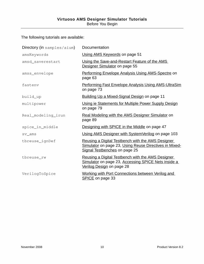
The following tutorials are available:
Directory (in samples/aium) Documentation
amsKeywords Using AMS Keywords on page 51
amsd_saverestart Using the Save-and-Restart Feature of the AMSDesigner Simulator on page 55
amss_envelope Performing Envelope Analysis Using AMS-Spectre onpage 63
fastenv Performing Fast Envelope Analysis Using AMS-UltraSimon page 73
build_up Building Up a Mixed-Signal Design on page 11
multipower Using ie Statements for Multiple Power Supply Designon page 79
Real_modeling_irun Real Modeling with the AMS Designer Simulator onpage 89
spice_in_middle Designing with SPICE in the Middle on page 47
sv_ams Using AMS Designer with SystemVerilog on page 103
tbreuse_ignDef Reusing a Digital Testbench with the AMS DesignerSimulator on page 23, Using Reuse Directives in Mixed-Signal Testbenches on page 25
tbreuse_rw Reusing a Digital Testbench with the AMS DesignerSimulator on page 23, Accessing SPICE Nets inside aVerilog Design on page 28
VerilogToSpice Working with Port Connections between Verilog andSPICE on page 33
November 2008 10 Product Version 8.2
Virtuoso AMS Designer Simulator Tutorials
3Building Up a Mixed-Signal Design
You can create a mixed-signal design consisting of Verilog-AMS and SPICE design units, andsimulate your design using irun. The irun program supports a broad mixed-language baseand offers a simple command-line interface for design verification. For more information, see“Using irun for AMS Simulation” in the Virtuoso AMS Designer Simulator User Guide.Additional features of irun include the following:
■ irun automatically determines the top-level design unit from Verilog or SystemVerilogsource files. (For other languages, you can use -top to specify the top-level design unit.)
■ irun supports SPICE-in-the-middle design.
■ irun supports the amsd block.
You can build up a mixed-signal design for AMS Designer simulation by
■ Converting a purely digital design into an AMS design by replacing one or more digitalblocks with SPICE or Spectre blocks (netlists), or
■ Stitching existing digital (Verilog) modules together with SPICE/Spectre subcircuits.
We will focus on the second of these two approaches using the build_up tutorial files.
We will demonstrate how to prepare and run the AMS Designer simulator for a designconsisting of SPICE netlists and Verilog modules. We will demonstrate single-step simulationusing irun and the amsd block. This use model is simpler than the ncvlog/ncelab/ncsimthree-step approach.
Important
Before starting this tutorial, see “Before You Begin” on page 9.
See the following topics for details:
■ Design Information on page 13
■ Organizing Design Files into One Directory on page 14
November 2008 11 Product Version 8.2
Virtuoso AMS Designer Simulator TutorialsBuilding Up a Mixed-Signal Design
■ Building the Testbench on page 15
■ Creating a Run Script for irun on page 17
■ Creating the AMS Control File on page 18
■ Specifying a Configuration for the Design on page 19
■ Specifying Connect Rules on page 20
■ Creating a Tcl File to Probe Digital Nodes on page 20
■ Creating Analog Probes in the Analog Control File on page 21
■ Running irun on page 22
November 2008 12 Product Version 8.2
Virtuoso AMS Designer Simulator TutorialsBuilding Up a Mixed-Signal Design
Design Information
The example we will use is a PLL design that consists of both SPICE netlists and Verilogcode. The design units for this example might come from analog and digital designcommunities separately. This PLL design consists of
■ a VCO (which happens to be a Verilog-A module in this case),
■ a digital frequency divider,
■ a digital frequency counter,
■ a phase detector (PD), and
■ a charge pump.
The VCO generates eight 400 MHz signals with different phases (p0, p45, p90, ... , p315).The design divides down one of the outputs (p0) by a factor of two before feeding into thephase detector (vcoclk). The other input to the phase detector is a 200 MHz reference clocksignal (refclk). When the two inputs to the phase detector are out-of-sync, the phasedetector generates corrective pulses to adjust the differential output voltages of the chargepump (vcop, vcom), which control the frequency of the VCO. When the PLL is in lock, thevcoclk and refclk signals are in phase and the VCO control signals V(vcop) andV(vcom) are stable.
The key signals are:
■ testbench.refclk
■ testbench.clk_p0_1x
■ testbench.clk_p0_4x
■ testbench.p1.vcom
■ testbench.p1.vcop
■ testbench.p0
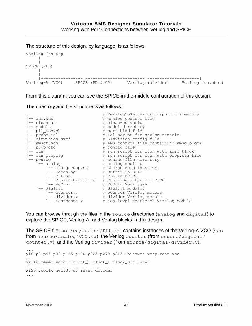
The design files consist of SPICE netlists and Verilog-A for analog design units, analog devicemodels, and Verilog modules for digital design units as follows:
.|-- .solutions # Hidden directory for reference|-- analog # Analog (SPICE) netlist| |-- ChargePump.sp # Charge pump subckt| |-- Gates.sp # Basic gates| |-- PLL.sp # PLL circuit, including all analog blocks| |-- PhaseDetector.sp # Phase detector subcircuit| '-- VCO.va # Verilog-A module
November 2008 13 Product Version 8.2
Virtuoso AMS Designer Simulator TutorialsBuilding Up a Mixed-Signal Design
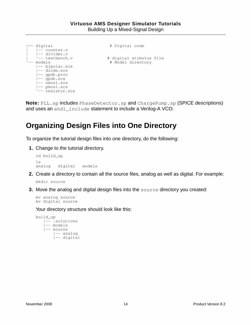
|-- digital # Digital code| |-- counter.v| |-- divider.v| '-- testbench.v # digital stimulus file'-- models # Model directory
|-- bipolar.scs|-- diode.scs|-- gpdk.proc|-- gpdk.scs|-- nmos1.scs|-- pmos1.scs'-- resistor.scs
Note: PLL.sp includes PhaseDetector.sp and ChargePump.sp (SPICE descriptions)and uses an ahdl_include statement to include a Verilog-A VCO.
Organizing Design Files into One Directory
To organize the tutorial design files into one directory, do the following:
1. Change to the tutorial directory.
cd build_up
lsanalog digital models
2. Create a directory to contain all the source files, analog as well as digital. For example:
mkdir source
3. Move the analog and digital design files into the source directory you created:
mv analog sourcemv digital source
Your directory structure should look like this:
build_up|-- .solutions|-- models|-- source
|-- analog|-- digital
November 2008 14 Product Version 8.2
Virtuoso AMS Designer Simulator TutorialsBuilding Up a Mixed-Signal Design
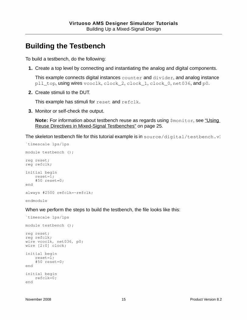
Building the Testbench
To build a testbench, do the following:
1. Create a top level by connecting and instantiating the analog and digital components.
This example connects digital instances counter and divider, and analog instancepll_top, using wires vcoclk, clock_2, clock_1, clock_0, net036, and p0.
2. Create stimuli to the DUT.
This example has stimuli for reset and refclk.
3. Monitor or self-check the output.
Note: For information about testbench reuse as regards using $monitor, see “UsingReuse Directives in Mixed-Signal Testbenches” on page 25.
The skeleton testbench file for this tutorial example is in source/digital/testbench.v:
`timescale 1ps/1ps
module testbench ();
reg reset;reg refclk;
initial beginreset=1;#50 reset=0;
end
always #2500 refclk=~refclk;
endmodule
When we perform the steps to build the testbench, the file looks like this:
`timescale 1ps/1ps
module testbench ();
reg reset;reg refclk;wire vcoclk, net036, p0;wire [2:0] clock;
initial beginreset=1;#50 reset=0;
end
initial beginrefclk=0;
end
November 2008 15 Product Version 8.2
Virtuoso AMS Designer Simulator TutorialsBuilding Up a Mixed-Signal Design
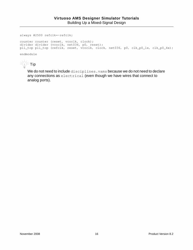
always #2500 refclk=~refclk;
counter counter (reset, vcoclk, clock);divider divider (vcoclk, net036, p0, reset);pll_top pll_top (refclk, reset, vcoclk, clock, net036, p0, clk_p0_1x, clk_p0_4x);
endmodule
Tip
We do not need to include disciplines.vams because we do not need to declareany connections as electrical (even though we have wires that connect toanalog ports).
November 2008 16 Product Version 8.2
Virtuoso AMS Designer Simulator TutorialsBuilding Up a Mixed-Signal Design
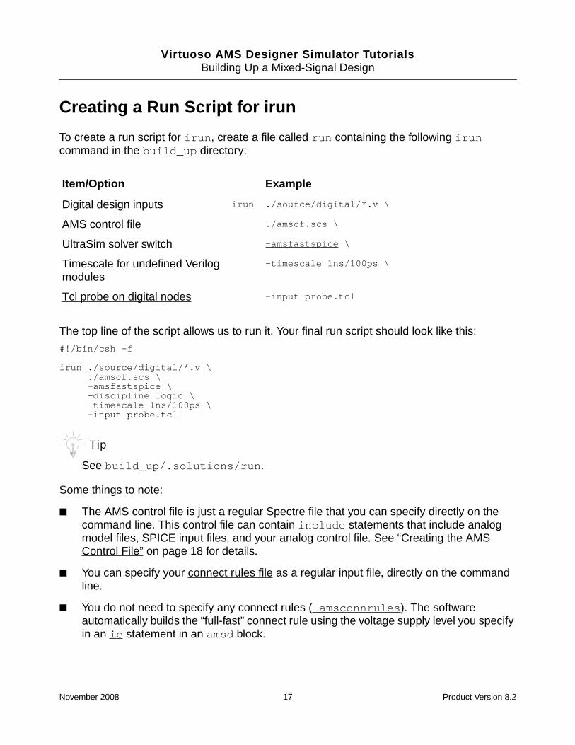
Creating a Run Script for irun
To create a run script for irun, create a file called run containing the following iruncommand in the build_up directory:
The top line of the script allows us to run it. Your final run script should look like this:
#!/bin/csh -f
irun ./source/digital/*.v \./amscf.scs \-amsfastspice \-discipline logic \-timescale 1ns/100ps \-input probe.tcl
Tip
See build_up/.solutions/run.
Some things to note:
■ The AMS control file is just a regular Spectre file that you can specify directly on thecommand line. This control file can contain include statements that include analogmodel files, SPICE input files, and your analog control file. See “Creating the AMSControl File” on page 18 for details.
■ You can specify your connect rules file as a regular input file, directly on the commandline.
■ You do not need to specify any connect rules (-amsconnrules). The softwareautomatically builds the “full-fast” connect rule using the voltage supply level you specifyin an ie statement in an amsd block.
Item/Option Example
Digital design inputs irun ./source/digital/*.v \
AMS control file ./amscf.scs \
UltraSim solver switch -amsfastspice \
Timescale for undefined Verilogmodules
-timescale 1ns/100ps \
Tcl probe on digital nodes -input probe.tcl
November 2008 17 Product Version 8.2
Virtuoso AMS Designer Simulator TutorialsBuilding Up a Mixed-Signal Design
Creating the AMS Control File
For this example, we will put the following statements in the AMS control file (which is justanother Spectre format input file that happens to contain one or more amsd blocks):
■ include statements for analog model files:
include "./models/resistor.scs" section=resinclude "./models/diode.scs" section=dioinclude "./models/pmos1.scs" section=nominclude "./models/nmos1.scs" section=nom
■ include statement for the SPICE input file:
include "./source/analog/PLL.sp"
■ include statement for the analog control file:
include "./acf.scs"
See “Creating Analog Probes in the Analog Control File” on page 21 for informationabout the contents of this file.
■ The amsd block:
amsd {portmap subckt=pll_top busdelim="_"config cell=pll_top use=spiceie vsup=2.0}
Tip
See build_up/.solutions/amscf.scs.
November 2008 18 Product Version 8.2
Virtuoso AMS Designer Simulator TutorialsBuilding Up a Mixed-Signal Design
Specifying a Configuration for the Design
You can use a config statement in the amsd block to specify a configuration for the design.You can put the amsd block in an ordinary Spectre or SPICE input file. You can include analogSPICE files, specify multiple disciplines and connect module information, simulation controlstatements, and so on.
For example, see build_up/.solutions/amscf.scs whose contents include:
*...include "./source/analog/PLL.sp"...amsd {
portmap subckt=pll_top busdelim="_"config cell=pll_top use=spice...}
The first line is a comment line, which is the convention for Spectre files. In the amsd block,the portmap statement tells the AMS Designer simulator how a SPICE subcircuit interfaceshould appear to the elaborator. The config statement specifies a SPICE version for thepll_top cell, while the rest of the design uses Verilog.
Note: If you are migrating from using a prop.cfg file, you will recognize the following asequivalent to the amsd block above:
cell pll_top{
string prop sourcefile="./source/analog/PLL.sp";string prop sourcefile_opts="-auto_bus";
}
Using irun and the amsd block simplifies setting up and running your simulations by notrequiring the various setup files that the three-step method required: cds.lib, worklib,prop.cfg, and so on.
November 2008 19 Product Version 8.2
Virtuoso AMS Designer Simulator TutorialsBuilding Up a Mixed-Signal Design
Specifying Connect Rules
Tip
If you are a new user or creating a new test case, we recommend you use an iestatement in an amsd block in an AMS control file (see “Creating the AMS ControlFile” on page 18) to automate the process of creating a custom discipline andconnect rule for connecting the custom discipline to the electrical discipline. Youdo not need to specify the connect module path or to compile any connect modules.The software automatically builds the “full-fast” connect rule using the voltagesupply level you specify and applies the custom discipline to domainless nets in yourdesign. You can find the set of connect rule files that Cadence provides inyour_install_dir/tools/affirma_ams/etc/connect_lib. Seeyour_install_dir/tools/affirma_ams/etc/connect_lib/README fordetailed information about them.
Another way to specify connect rules when you run irun is to use the -amsconnrulescommand-line option:
irun -amsconnrules nameOfConnRules ...
For example, to specify the 1.8 V full-fast connect rules, you can specify the connect rules fileon the irun command line (just like any other input file) and the set of connect rules, byname, using the -amsconnrules command-line option as follows:
irun ./source/digital/ConnRules18.vams -amsconnrules ConnRules_18V_full_fast ...
Creating a Tcl File to Probe Digital Nodes
To probe digital nodes and save that information to a database file called waves.shm, createa Tcl file (probe.tcl) containing the following commands:
database -open waves -into waves.shm -defaultprobe -create -database waves -all -depth allprobe -create -database waves testbench.refclkprobe -create -database waves testbench.clk_p0_1xprobe -create -database waves testbench.clk_p0_4xprobe -create -database waves testbench.p0
#simvision -input simvision.svrunexit
Tip
You can use the one in build_up/.solutions.
November 2008 20 Product Version 8.2
Virtuoso AMS Designer Simulator TutorialsBuilding Up a Mixed-Signal Design
The database command opens the waves.shm waveform database file. The probecommands create probes for digital nodes. Notice that you can also specify simulation controlcommands (such as run) in a Tcl file.
To specify the Tcl file on the irun command line, use the -input command-line option:
irun ... -input probe.tcl ...
Creating Analog Probes in the Analog Control File
In addition to specifying analog simulation control statements (such as the .tran statementand the UltraSim .usim_opt statements), you can use the UltraSim .probe statement tospecify analog probes in the analog control file. Create the following file in the build_updirectory and call it acf.scs:
***********************************simulator lang=spice lookup=spectre***********************************
*--------------------------------------------------------** UltraSim Analysis Options*--------------------------------------------------------*.tran 1ns 200ns
*--------------------------------------------------------** UltraSim Simulator Options*--------------------------------------------------------**ultrasim: .usim_opt method=gear2*ultrasim: .usim_opt progress_p=10
.probe v(*) depth=3 preserve=port
.probe v(testbench.p1.vcom) v(testbench.p1.vcop)
.end
Tip
You can also copy build_up/.solutions/acf.scs to the build_up directory.
The first .probe statement saves all analog nodes to a hierarchical depth of three. Thesecond .probe statement requests a selective save of particular analog nodes.
The simulator saves all analog waveforms into the same database that contains the digitalwaveforms (waves.shm), so you can display both analog and digital waveforms in the samewaveform viewer.
November 2008 21 Product Version 8.2
Virtuoso AMS Designer Simulator TutorialsBuilding Up a Mixed-Signal Design
Running irun
Review the irun run script (see “Creating a Run Script for irun” on page 17 orbuild_up/.solutions/run). To run the script, type the following command:
./run
You can use SimVision to verify the waveforms when the simulation has finished. You can lookat the irun.log file for simulation messages.
November 2008 22 Product Version 8.2
Virtuoso AMS Designer Simulator Tutorials
4Reusing a Digital Testbench with the AMSDesigner Simulator
When you take a purely digital design and replace one or more digital blocks with SPICE orSpectre design units, you can find yourself with a purely digital testbench that now has someout-of-module references (OOMRs) to SPICE items. Even with such references, you can addsettings and directives to the testbench such that you can reuse it in the analog/mixed-signaldomain where you simulate using the Virtuoso® AMS Designer simulator.
Consider the following example statements that might contain OOMRs to SPICE once youreplace a Verilog module (say, timer) with a SPICE or Spectre netlist.
■ force testbench.dut.timer.data[0] = 0
■ if (testbench.dut.timer.data[0] ==1 ) counter = 0
■ wire a=((testbench.dut.timer.data[0] === 1) ||(testbench.duv.timer.data[1] === 0
■ always @(posedge testbench.dut.timer.data[0] counter = 1
You can choose whether to default the value of the OOMR to X (digital “unknown”) or to ignoreit altogether. Yet another alternative is to write your testbench to use special “conversion”instances so that you can access SPICE nets in a Verilog design.
Note: The design we will use to demonstrate these methods is approximately the same asthe one we used in “Building Up a Mixed-Signal Design” on page 11.
Tip
You can also use the -ignore_spice_oomr and -default_spice_oomrcommand-line options to specify how you want the software to manageout-of-module references in digital statements when you substitute a SPICE blockfor a purely digital (Verilog) block. For more information, see “Using aCommand-Line Option to Manage Out-of-Module References to SPICE” in theVirtuoso AMS Designer Simulator User Guide.
November 2008 23 Product Version 8.2
Virtuoso AMS Designer Simulator TutorialsReusing a Digital Testbench with the AMS Designer Simulator
Important
Before starting this tutorial, see “Before You Begin” on page 9.
See the following topics for details:
■ Using Reuse Directives in Mixed-Signal Testbenches on page 25
■ Accessing SPICE Nets inside a Verilog Design on page 28
November 2008 24 Product Version 8.2
Virtuoso AMS Designer Simulator TutorialsReusing a Digital Testbench with the AMS Designer Simulator
Using Reuse Directives in Mixed-Signal Testbenches
If you have constructs or techniques to verify your mixed-signal simulation using the samedigital testbench, you can use the `ams_testbench_reuse_ignore and`ams_testbench_reuse_default_value directives to specify how you want thesoftware to manage out-of-module references (OOMRs) in digital statements when yousubstitute a SPICE block for a purely digital (Verilog) block. You can use these directives inconjunction with the following statements:
■ if statements
■ $display/$monitor statements
■ Procedural assignments, including blocking and nonblocking
■ force and release procedural statements
■ Continuous assignments
■ Sequential blocks (where the out-of-module reference to SPICE is in a delay or eventcontrol expression)
Consider the following testbench, which you will find in the tbreuse_ignDef tutorialdirectory (tbreuse_ignDef/source/digital/testbench.v). Notice that the$monitor statements in the third initial … begin block have OOMRs to SPICE whenyou substitute a SPICE subcircuit for the pll_top design unit.
`timescale 1ps/1ps
module testbench ();
reg reset_d;reg reset;reg refclk;wire vcoclk, clock_2, clock_1, clock_0, net036, p0;
initial beginreset_d=1;reset=1;#200 reset_d=0;
reset=0;#100000 reset_d=1;
reset=1;#100 reset_d=0;
reset=0;end
initial beginrefclk=0;#200 refclk=1;
end
initial begin
November 2008 25 Product Version 8.2
Virtuoso AMS Designer Simulator TutorialsReusing a Digital Testbench with the AMS Designer Simulator
$monitor (testbench.pll_top.vcom);$monitor (testbench.pll_top.vcop);
end
always #2500 refclk=~refclk;
counter counter (reset_d, vcoclk, clock_2, clock_1, clock_0);divider divider (vcoclk, net036, p0, reset_d);pll_top pll_top (refclk, reset, vcoclk, clock_2, clock_1, clock_0, net036, p0,clk_p0_1x, clk_p0_4x);
endmodule
See the following topics for information about using the testbench-reuse directives to ignorethe OOMRs or to assign a value of “1’bx” (digital “unknown”):
■ Using the `ams_testbench_reuse_ignore Directive on page 26
■ Using the `ams_testbench_reuse_default_value Directive on page 27
Using the `ams_testbench_reuse_ignore Directive
You can use the `ams_testbench_reuse_ignore directive to cause the simulator toignore out-of-module references in digital statements that occur when you substitute a SPICEblock for a purely digital (Verilog) block. When you use the`ams_testbench_reuse_ignore directive, the software ignores any digital statementsthat contain out-of-module references to SPICE blocks. For example:
...`ams_testbench_reuse_ignore
initial begin$monitor (testbench.pll_top.vcom);$monitor (testbench.pll_top.vcop);
end
`end_ams_testbench_reuse_ignore...
To run this tutorial example, do the following:
1. Edit tbreuse_ignDef/source/digital/testbench.v to remove the // commentdelimiters from the beginning of the lines containing the`ams_testbench_reuse_ignore and `end_ams_testbench_reuse_ignoredirectives.
2. Type ./run on the command line in the tbreuse_ignDef tutorial directory.
You can view simulation messages in the irun.log file.
November 2008 26 Product Version 8.2
Virtuoso AMS Designer Simulator TutorialsReusing a Digital Testbench with the AMS Designer Simulator
See also “Reusing Mixed-Signal Testbenches“ in the Virtuoso AMS Designer Simulator UserGuide.
Using the `ams_testbench_reuse_default_value Directive
You can use the `ams_testbench_reuse_default_value directive to cause thesimulator to assign a value of 1’bx to out-of-module references in digital statements thatoccur when you substitute a SPICE block for a purely digital (Verilog) block.
For example:
...`ams_testbench_reuse_default_value
initial begin$monitor (testbench.pll_top.vcom);$monitor (testbench.pll_top.vcop);
end
`end_ams_testbench_reuse_default_value...
To run this tutorial example, do the following:
1. Edit tbreuse_ignDef/source/digital/testbench.v to remove the // commentdelimiters from the beginning of the lines containing the`ams_testbench_reuse_default_value and`end_ams_testbench_reuse_default_value directives.
2. Type ./run on the command line in the tbreuse_ignDef tutorial directory.
You can view simulation messages in the irun.log file.
See also “Reusing Mixed-Signal Testbenches“ in the Virtuoso AMS Designer Simulator UserGuide.
November 2008 27 Product Version 8.2
Virtuoso AMS Designer Simulator TutorialsReusing a Digital Testbench with the AMS Designer Simulator
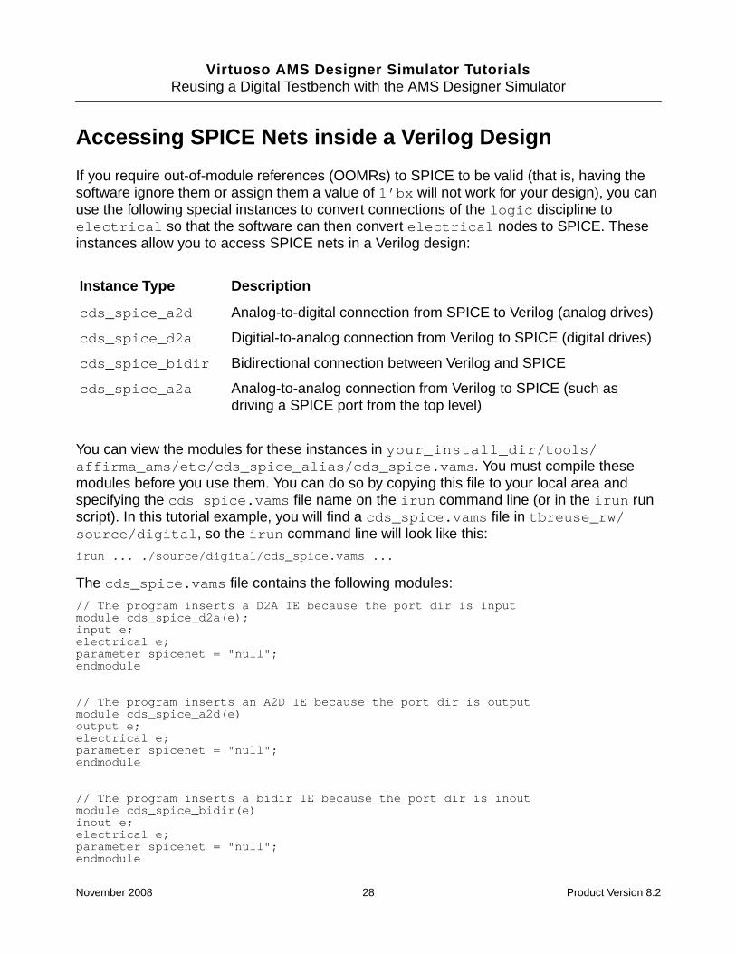
Accessing SPICE Nets inside a Verilog Design
If you require out-of-module references (OOMRs) to SPICE to be valid (that is, having thesoftware ignore them or assign them a value of 1’bx will not work for your design), you canuse the following special instances to convert connections of the logic discipline toelectrical so that the software can then convert electrical nodes to SPICE. Theseinstances allow you to access SPICE nets in a Verilog design:
You can view the modules for these instances in your_install_dir/tools/affirma_ams/etc/cds_spice_alias/cds_spice.vams. You must compile thesemodules before you use them. You can do so by copying this file to your local area andspecifying the cds_spice.vams file name on the irun command line (or in the irun runscript). In this tutorial example, you will find a cds_spice.vams file in tbreuse_rw/source/digital, so the irun command line will look like this:
irun ... ./source/digital/cds_spice.vams ...
The cds_spice.vams file contains the following modules:
// The program inserts a D2A IE because the port dir is inputmodule cds_spice_d2a(e);input e;electrical e;parameter spicenet = "null";endmodule
// The program inserts an A2D IE because the port dir is outputmodule cds_spice_a2d(e)output e;electrical e;parameter spicenet = "null";endmodule
// The program inserts a bidir IE because the port dir is inoutmodule cds_spice_bidir(e)inout e;electrical e;parameter spicenet = "null";endmodule
Instance Type Description
cds_spice_a2d Analog-to-digital connection from SPICE to Verilog (analog drives)
cds_spice_d2a Digitial-to-analog connection from Verilog to SPICE (digital drives)
cds_spice_bidir Bidirectional connection between Verilog and SPICE
cds_spice_a2a Analog-to-analog connection from Verilog to SPICE (such asdriving a SPICE port from the top level)
November 2008 28 Product Version 8.2
Virtuoso AMS Designer Simulator TutorialsReusing a Digital Testbench with the AMS Designer Simulator
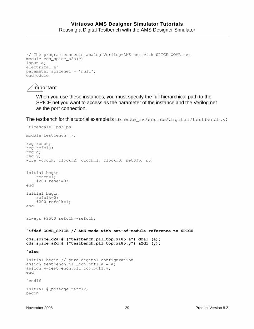
// The program connects analog Verilog-AMS net with SPICE OOMR netmodule cds_spice_a2a(e)input e;electrical e;parameter spicenet = "null";endmodule
Important
When you use these instances, you must specify the full hierarchical path to theSPICE net you want to access as the parameter of the instance and the Verilog netas the port connection.
The testbench for this tutorial example is tbreuse_rw/source/digital/testbench.v:
`timescale 1ps/1ps
module testbench ();
reg reset;reg refclk;reg a;reg y;wire vcoclk, clock_2, clock_1, clock_0, net036, p0;
initial beginreset=1;#200 reset=0;
end
initial beginrefclk=0;#200 refclk=1;
end
always #2500 refclk=~refclk;
`ifdef OOMR_SPICE // AMS mode with out-of-module reference to SPICE
cds_spice_d2a # ("testbench.pll_top.xi85.a") d2a1 (a);cds_spice_a2d # ("testbench.pll_top.xi85.y") a2d1 (y);
`else
initial begin // pure digital configurationassign testbench.pll_top.buf1.a = a;assign y=testbench.pll_top.buf1.y;end
`endif
initial @(posedge refclk)begin
November 2008 29 Product Version 8.2
Virtuoso AMS Designer Simulator TutorialsReusing a Digital Testbench with the AMS Designer Simulator
$monitor (a, y);end
initial begin# 1000 force a = 0;
end
counter counter (reset, vcoclk, clock_2, clock_1, clock_0);divider divider (vcoclk, net036, p0, reset);pll_top pll_top (refclk, reset, vcoclk, clock_2, clock_1, clock_0, net036, p0,clk_p0_1x, clk_p0_4x);
endmodule
When we replace the pll_top cell with a SPICE version, the assign statement contains anout-of-module reference (OOMR) to SPICE. By adding the `ifdef block and defining theOOMR_SPICE macro on the irun command line (-define OOMR_SPICE), we canconditionally use the special conversion instances, cds_spice_d2a and cds_spice_a2d,to establish valid connections between SPICE and Verilog. Here is the irun command line(which you can view in tbreuse_rw/run):
irun ./source/digital/*.v \./source/digital/cds_spice.vams \./amscf.scs \-define OOMR_SPICE \-amsfastspice \-iereport \-timescale 1ns/100ps \-input probe.tcl
The cds_spice_d2a special instance converts node a to a true SPICE hierarchical name,testbench.pll_top.xi85.a, where xi85 is a SPICE instance name.
Similarly, the cds_spice_a2d special instance converts node y to a true SPICE hierarchicalname, testbench.pll_top.xi85.y, where xi85 is a SPICE instance name.
Note: The xi85 instance appears in source/analog/PLL.sp, in the pll_top subcircuit.The subcircuit definition for buf4_g14 (of which xi85 is an instance) appears in source/analog/Gates.sp. This buffer has nodes a and y.
Only when you run irun with the -define option to define the OOMR_SPICE macro doesthe program use these special conversion instances.
You can look in the irun.log file for the interface element (IE) report. The first IE istestbench.a__L2E_2__electrical, which corresponds to the cds_spice_d2a. Theinstance name, d2a1, becomes driver pin testbench.d2a1. The second IE istestbench.y__E2L_2__electrical, which corresponds to the cds_spice_a2d.Because the driver is from SPICE, the elaborator does not have driver information.
----------IE report -------------
Automatically inserted instance: testbench.a__L2E_2__electrical (merged):connectmodule name: L2E_2,
November 2008 30 Product Version 8.2
Virtuoso AMS Designer Simulator TutorialsReusing a Digital Testbench with the AMS Designer Simulator
inserted across signal: aand ports of discipline: electricalSensitivity infomation:
No Sensitivity infoDiscipline of Port (Din): logic, Digital portDrivers of port Din:
(testbench.d2a1) input port 1, bit 0 (./source/digital/testbench.v:29)Loads of port Din:
Load: VST_S_BLOCKING_ASSIGNMENT, Line 75, Index 0, in: testbench.a__L2E_2__electrical
Discipline of Port (Aout): electrical, Analog portAutomatically inserted instance: testbench.y__E2L_2__electrical (merged):
connectmodule name: E2L_2,inserted across signal: yand ports of discipline: electricalSensitivity infomation:
No Sensitivity infoDiscipline of Port (Ain): electrical, Analog portDiscipline of Port (Dout): logic, Digital portDrivers of port Dout: No driversLoads of port Dout: No loads
See also “Accessing SPICE Nets inside a Verilog Design“ in the Virtuoso AMS DesignerSimulator User Guide.
November 2008 31 Product Version 8.2

Virtuoso AMS Designer Simulator TutorialsReusing a Digital Testbench with the AMS Designer Simulator
November 2008 32 Product Version 8.2
Virtuoso AMS Designer Simulator Tutorials
5Working with Port Connections betweenVerilog and SPICE
The AMS Designer simulator in the AIUM1 flow supports designs that have Verilog on top andSPICE in the middle. In designs such as these, it is important for the signals to propagatebetween Verilog and SPICE in an expected way. Port direction, bus ordering, andconcatenated expressions are some of the issues that can affect these connections.
Important
Before starting these tutorials, see “Before You Begin” on page 9.
The four tutorials we will explore are in the VerilogToSpice directory:
See the following topics for more information:
■ Using Port Expressions on page 34
■ Binding SPICE Ports to Verilog Ports on page 36
See also "Binding Ports" in the design verification chapter of the Virtuoso® AMS DesignerSimulator User Guide.
1. AIUM stands for AMS Designer Incisive Use Model.
Subdirectory Description
auto_bus How to use the “autobus” feature for regular port mapping
port_expression How to use port expressions to combine different signal types(such as logic, reg, electrical) into one item in a port list
port_mapping How to set up and use a customized port-bind file
veri_file How to specify a Verilog file for corresponding SPICEreplacement cell port mappings
November 2008 33 Product Version 8.2
Virtuoso AMS Designer Simulator TutorialsWorking with Port Connections between Verilog and SPICE
Using Port Expressions
For information about port expressions you can use when connecting Verilog to SPICE, see“Using Port Expressions when Connecting to Analog“ in the Virtuoso AMS DesignerSimulator User Guide.
To begin the tutorial on port expressions, do the following:
1. Change to the port_expression tutorial subdirectory. For example, assuming you arein the directory where you installed the tutorial files:
cd VerilogToSpice/port_expression
2. Open test.vams and look at module top which contains the following five analogchild block instances:
analog_child child1( {{a, b, c, 2'b10}, {d, c, a, b, 2'b10}} );analog_child child2( {{a, {2{b, 2'b10}}}, {a, b, 2'b10}} );analog_child child3( {{top.d1.r, top.d1.p, top.d1.l, top.d1.l},
{top.d1.r, top.d1.p, top.d1.l, 2'b10}} );analog_child child4( {2{top.d1.r, top.d1.p, top.d1.l, top.d1.l}} );dummy d1();analog_child child5( {{2{2'b10, 2'b10}}, {2'b10, in_bit, in_bit, 2'b10}} );
child1 contains recursive concatenation; child2 has multiple concatenations inside aconcatenation; child3 has multiple concatenation expressions with an out-of-modulereference (OOMR) on a port; child4 has multiple concatenations including an OOMRexpression; child5 has multiple concatenations inside a concatenation.
Note: You might also notice child6, which contains a multiply-recursive concatenation:
//analog_child child6( {2{{2{a[1], 1'b1}},{2'b01,b}}} );
The software does not support this form of concatenation at this time.
3. To run the simulation, use the run script:
./run
Note: The run script looks like this:
#! /bin/csh -firun ./test.vams \
amscf.scs \-amsfastspice \-iereport \-timescale 1ns/1ns \-input probe.tcl
4. Open the irun.log file and look at the IE report at the connect modules for constantexpressions, such as:
Automatically inserted instance: top.\Exp0=2'b10__L2E_2__electrical (merged):connectmodule name: L2E_2,
November 2008 34 Product Version 8.2
Virtuoso AMS Designer Simulator TutorialsWorking with Port Connections between Verilog and SPICE
inserted across signal: Exp0=2'b10and ports of discipline: electricalSensitivity infomation:
No Sensitivity infoDiscipline of Port (Din): logic, Digital port
The inserted across signal line indicates the expression the software uses for thesignal. The software inserts L2E connect modules for logic-to-electrical connections.
To run SimVision to look at all the port signals and to verify their values, do the following:
1. Change to the VerilogToSpice/port_expression/top.shm directory:
cd top.shm
2. Run SimVision:
simvision &
3. In SimVision, choose File – Open Database.
4. Select top.trn.
5. View the port signals and verify that the out-of-module references on ports return correctvalues.
6. When you are finished, choose File – Exit SimVision.
7. Run the clean-up script:
./clean_up
November 2008 35 Product Version 8.2

Virtuoso AMS Designer Simulator TutorialsWorking with Port Connections between Verilog and SPICE
Binding SPICE Ports to Verilog Ports
The following tutorial exercises demonstrate three methods for binding SPICE ports to Verilogports:
■ Using the autobus Feature on page 37
■ Using a Port-Bind File on page 41
■ Using a Verilog File to Specify Port Binding for a Corresponding SPICE Subcircuit onpage 45
For assistance in deciding which method is best for your design, see "Binding Ports" in theVirtuoso AMS Designer Simulator User Guide.
November 2008 36 Product Version 8.2
Virtuoso AMS Designer Simulator TutorialsWorking with Port Connections between Verilog and SPICE
Using the autobus Feature
When mapping SPICE ports to Verilog ports, you can use the autobus feature if your designcontains regular port connectivity with uniform case mapping and identical bus ordering.Using the autobus feature, you can connect Verilog vector buses to SPICE scalar portsdirectly. You can also make port connections by name.
Note: See also "Binding Ports using autobus" in the Virtuoso® AMS Designer SimulatorUser Guide.
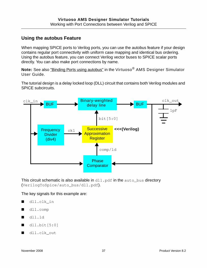
The tutorial design is a delay locked loop (DLL) circuit that contains both Verilog modules andSPICE subcircuits.
This circuit schematic is also available in dll.pdf in the auto_bus directory(VerilogToSpice/auto_bus/dll.pdf).
The key signals for this example are:
■ dll.clk_in
■ dll.comp
■ dll.ld
■ dll.bit[5:0]
■ dll.clk_out
Binary-weighteddelay line BUF
FrequencyDivider(div4)
PhaseComparator
BUF
SuccessiveApproximation
Register
clk_in
ck1
bit[5:0]
clk_out
1pF
comp/ld
<<<(Verilog)
November 2008 37 Product Version 8.2
Virtuoso AMS Designer Simulator TutorialsWorking with Port Connections between Verilog and SPICE
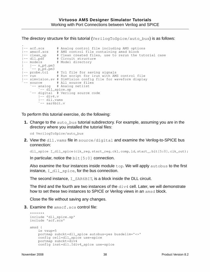
The directory structure for this tutorial (VerilogToSpice/auto_bus) is as follows:
.|-- acf.scs # Analog control file including AMS options|-- amscf.scs # AMS control file containing amsd block|-- clean_up # Clean created files, use to rerun the tutorial case|-- dll.pdf # Circuit structure|-- models # Model directory| |-- n_p6.pm3| `-- p_p6.pm3|-- probe.tcl # Tcl file for saving signals|-- run # Run script for irun with AMS control file|-- simvision.sv # SimVision config file for waveform display`-- source # All source files
`-- analog # Analog netlist`-- dll_spice.sp
`-- digital # Verilog source code|-- div4.v|-- dll.vams`-- sar6bit.v
To perform this tutorial exercise, do the following:
1. Change to the auto_bus tutorial subdirectory. For example, assuming you are in thedirectory where you installed the tutorial files:
cd VerilogToSpice/auto_bus
2. View the dll.vams file in source/digital and examine the Verilog-to-SPICE busconnection:
dll_spice I_dll_spice(clk_reg,start_reg,ck1,comp,ld,start_,bit[5:0],clk_out);
In particular, notice the bit[5:0] connection.
Also examine the four instances inside module top. We will apply autobus to the firstinstance, I_dll_spice, for the bus connection.
The second instance, I_SAR6BIT, is a block inside the DLL circuit.
The third and the fourth are two instances of the div4 cell. Later, we will demonstratehow to set these two instances to SPICE or Verilog views in an amsd block.
Close the file without saving any changes.
3. Examine the amscf.scs control file:
*******include "dll_spice.sp"include "acf.scs"
amsd {ie vsup=5portmap subckt=dll_spice autobus=yes busdelim="<>"config cell=dll_spice use=spiceportmap subckt=div4config inst=dll.Idiv4_spice use=spice
November 2008 38 Product Version 8.2
Virtuoso AMS Designer Simulator TutorialsWorking with Port Connections between Verilog and SPICE
portmap module=div4 reffile="source/digital/div4.v"config inst=dll.I_dll_spice.XI69 use=hdl}
The first line is a comment line, complying with SPICE file format requirements. The fileincludes the analog netlist, dll_spice.sp, and the top-level analog control file,acf.scs (which includes AMS options as well as analysis commands). The iestatement specifies connect module parameters. The first portmap statement in theamsd block specifies two options that affect Verilog to SPICE bus connections:
autobus=yes // Use autobus connection featurebusdelim="<>" // Specifies the bus delimitor
The second portmap/config statement pair specifies the Idiv4_spice instance ofthe div4 cell at top level as a SPICE view. This is a SPICE-on-leaf example:
portmap subckt=div4config inst=dll.Idiv4_spice use=spice
The third portmap/config statement pair specifies the XI69 instance of the div4 cell,inside I_dll_spice, as a Verilog view. This is a SPICE-in-the-middle example:
portmap module=div4 reffile="source/digital/div4.v"config inst=dll.I_dll_spice.XI69 use=hdl
Important
You must specify the full path to the instance when you use the inst parameter.See also the inst parameter description in "Using an amsd Block" in the VirtuosoAMS Designer Simulator User Guide.
Close the file without saving any changes.
4. To run the example, use the run script:
./run
The software creates a port-bind file in the portmap_files directory: dll_spice.pb.You can use this file to specify port bindings, if it meets your requirements. Theautobus=yes specifier in the portmap statement causes the software to write thefollowing line to the port-bind file:
{ bit<5>, bit<4>, bit<3>, bit<2>, bit<1>, bit<0> }: bit[5:0] dir=inout
You do not need to use this port-bind file for this tutorial. To see how to use a port-bindfile, see “Using a Port-Bind File” on page 41.
November 2008 39 Product Version 8.2
Virtuoso AMS Designer Simulator TutorialsWorking with Port Connections between Verilog and SPICE
5. Use SimVision to explore the waveform results:
a. Type simvision & on the command line.
b. In SimVision, choose File – Open Database.
c. Select the waves.trn file in waves.shm and click Open.
d. Examine the SPICE signals inside Idiv4_spice, and the Verilog signals insideIdiv4_behav and I_dll_spice.XI69. Compare the input and output of theseinstances; observe the divide-by-four clock; observe which signal is digital andwhich is analog.
e. When you are finished exploring waveforms, choose File – Exit SimVision.
6. You can clean up the example files by running the clean-up script in the auto_bustutorial directory:
./clean_up
Information about Bus Mapping and the prop.cfg File for Customers Migrating from aPrevious Version of the AMS Designer Simulator
If you are migrating from a previous version of the AMS Designer simulator, you might recallthat you had to break down connections between Verilog vector buses and SPICE scalarports and pass the net connections by order. For example:
module verilog;wire [0:5] v;analog_top xana_top ( v[0], v[1], v[2], v[3], v[4], v[5] );endmodule.subckt analog_top p<0> p<1> p<2> p<3> p<4> p<5>....ends
With the autobus feature, you no longer need to take the time to edit your connections in thisway. The autobus feature can save you a great deal of time, especially in the case of busvectors with a large number of bits.
November 2008 40 Product Version 8.2
Virtuoso AMS Designer Simulator TutorialsWorking with Port Connections between Verilog and SPICE
Using a Port-Bind File
If you need to customize port mapping information because your design contains complicatedbus forms or you require mixed-case mappings, you can use a port-bind file. In your port-bindfile, you can specify port mappings for mixed ascending/descending bus order, signalconcatenations in buses, as well as mixed-case port mappings. You can start with theautobus-generated port-bind file (*.pb) and edit it to your requirements, or you can create aport-bind file from scratch. For more information, see "Binding Ports using a Port Bind File"in the Virtuoso® AMS Designer Simulator User Guide.
Note: For information about how to format port mappings, see "Creating a Customized Port-Bind File" in the Virtuoso AMS Designer Simulator User Guide.
Important
You cannot connect a SystemVerilog net directly to a SPICE port.
To specify the port-bind file, use the portmap statement in an amsd block as follows:
include "analog_top.sp"amsd {
portmap subckt=analog_top file="analog_top.pb"config cell=analog_top use=spice}
The tutorial design consists of a PLL circuit with five major blocks:
■ Voltage-controlled oscillator (VCO, a Verilog-A block)
■ Phase detector (a SPICE block)
■ Charge pump (a SPICE block)
■ Divider (a Verilog block)
■ Counter (a Verilog block)
The top-level testbench is a Verilog module that instantiates the pll_top SPICE block.Inside the pll_top SPICE block, the VCO outputs eight evenly-spaced 400 MHz clocks, 45degree phase apart from each other. One output clock then passes through a divider andfeeds back into the phase detector (vcoclk). The phase detector (PD) compares theincoming clock signal with the VCO output clock and produces either an up or a down signalto control the charging or discharging of the charge pump (CP). As a result, the PD eitherraises or lowers the VCO output clock frequency to bring it back in sync with the incomingclock. When the feedback loop becomes stable, the design locks the VCO frequency to thatof the incoming signal.
November 2008 41 Product Version 8.2
Virtuoso AMS Designer Simulator TutorialsWorking with Port Connections between Verilog and SPICE
The structure of this design, by language, is as follows:
Verilog (on top)||
SPICE (PLL)|||-----------------|------------------------|---------------------|
Verilog-A (VCO) SPICE (PD & CP) Verilog (divider) Verilog (counter)
From this diagram, you can see the SPICE-in-the-middle configuration of this design.
The directory and file structure is as follows:
. # VerilogToSpice/port_mapping directory|-- acf.scs # analog control file|-- clean_up # clean-up script|-- models # model directory|-- pll_top.pb # port-bind file|-- probe.tcl # Tcl script for saving signals|-- simvision.svcf # SimVision config file|-- amscf.scs # AMS control file containing amsd block|-- prop.cfg # config file|-- run # run script for irun with amsd block|-- run_propcfg # run script for irun with prop.cfg file`-- source # source file directory
`-- analog # analog netlist|-- ChargePump.sp # Charge Pump in SPICE|-- Gates.sp # Buffer in SPICE|-- PLL.sp # PLL in SPICE|-- PhaseDetector.sp # Phase Detector in SPICE`-- VCO.va # VCO in Verilog-A
`-- digital # digital modules|-- counter.v # counter Verilog module|-- divider.v # divider Verilog module`-- testbench.v # top-level testbench Verilog module
You can browse through the files in the source directories (analog and digital) toexplore the SPICE, Verilog-A, and Verilog blocks in this design.
The SPICE file, source/analog/PLL.sp, contains instances of the Verilog-A VCO (vcofrom source/analog/VCO.va), the Verilog counter (from source/digital/counter.v), and the Verilog divider (from source/digital/divider.v):
...yi0 p0 p45 p90 p135 p180 p225 p270 p315 ibiasvco vcop vcom vco...xi116 reset vcoclk clock_2 clock_1 clock_0 counter...xi20 vcoclk net036 p0 reset divider...
November 2008 42 Product Version 8.2

Virtuoso AMS Designer Simulator TutorialsWorking with Port Connections between Verilog and SPICE
To run this tutorial example, do the following:
1. Change to the port_mapping directory.
For example, from the VerilogToSpice directory, type
cd port_mapping
2. Examine the reference to the port-bind file, pll_top.pb, in the portmap statement inthe amsd block in amscf.scs:
***********include "./source/analog/PLL.sp"include "./models/resistor.scs" section=resinclude "./models/diode.scs" section=dioinclude "./models/pmos1.scs" section=nominclude "./models/nmos1.scs" section=nominclude "acf.scs"
amsd{ie vsup=1.8portmap subckt=pll_top file="pll_top.pb"config cell=pll_top use=spiceportmap module=divider reffile="./source/digital/divider.v"config cell=divider use=hdlportmap module=counter reffile="./source/digital/counter.v"config cell=counter use=hdl}
3. Examine the port-bind file, pll_top.pb:
refclk : refclk dir=inoutreset : RESET dir=inout{p0_clk_1, p0_clk_0} : P0_CLK[0:1] dir=inout
The node specification in the subcircuit definition for the pll_top SPICE block (insource/analog/PLL.sp) corresponds to the identifiers to the left of the colon in theport-bind file (the actualName):
.subckt pll_top refclk reset p0_clk_1 p0_clk_0
The Verilog identifiers in the pll_top instance statement in the top-level Verilogtestbench (in source/digital/testbench.v) correspond to the identifiers on theright side of the colon in the port-bind file (the portName):
...module testbench ();
reg RESET;reg refclk;wire [0:1] clk_out;...pll_top p1(.refclk(refclk), .RESET(RESET), .P0_CLK(clk_out));...
November 2008 43 Product Version 8.2
Virtuoso AMS Designer Simulator TutorialsWorking with Port Connections between Verilog and SPICE
The reset : RESET mapping in pll_top.pb represents a mixed-case binding(lowercase reset in the subcircuit definition; uppercase RESET in the Verilog regdeclaration). The {p0_clk_1, p0_clk_0} : P0_CLK[0:1] binding in pll_top.pbdemonstrates how you can bind a SPICE bus whose order is descending (p0_clk_1p0_clk_0 in the subcircuit definition) to a Verilog bus whose order is ascending (wire[0:1] clk_out; in module testbench). The port-bind file lets you manage thesecomplex bindings.
4. To run this tutorial example, use the run script:
./run
When the simulation finishes, SimVision windows appear.
Note: The irun command in the run script looks like this:
5. (Optional) In the SimVision Waveform window, examine the key signals.
6. When finished using SimVision, choose File – Exit SimVision.
7. (Optional) To remove simulation-generated files, run the clean-up script:
./clean_up
irun \
-messages \ Request verbose messages
-amsf \ Request UltraSim solver
-access +rw \ Turn on read/write object access
-timescale 1ns/100ps \ Set timescale for digital solver
-iereport \ Request interface element report
amscf.scs \ Input file: AMS controls
-input probe.tcl \ Tcl probes
./source/digital/ *.v \ Verilog input files
November 2008 44 Product Version 8.2
Virtuoso AMS Designer Simulator TutorialsWorking with Port Connections between Verilog and SPICE
Using a Verilog File to Specify Port Binding for a Corresponding SPICESubcircuit
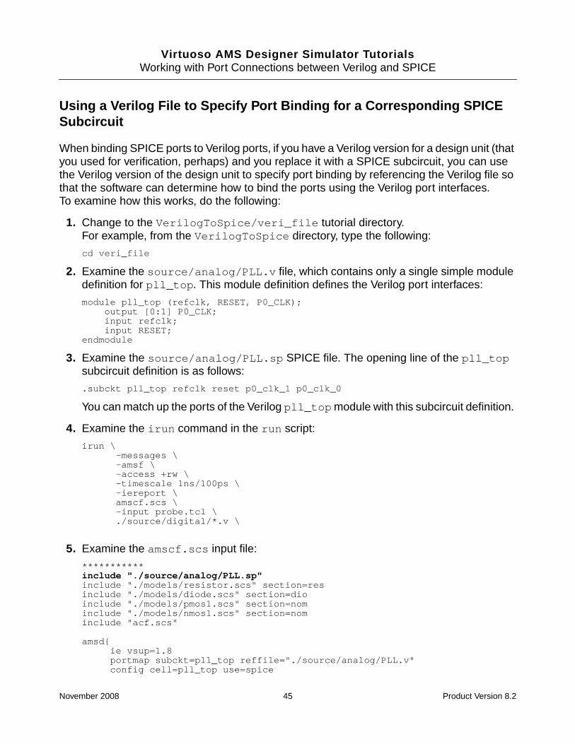
When binding SPICE ports to Verilog ports, if you have a Verilog version for a design unit (thatyou used for verification, perhaps) and you replace it with a SPICE subcircuit, you can usethe Verilog version of the design unit to specify port binding by referencing the Verilog file sothat the software can determine how to bind the ports using the Verilog port interfaces.To examine how this works, do the following:
1. Change to the VerilogToSpice/veri_file tutorial directory.For example, from the VerilogToSpice directory, type the following:
cd veri_file
2. Examine the source/analog/PLL.v file, which contains only a single simple moduledefinition for pll_top. This module definition defines the Verilog port interfaces:
module pll_top (refclk, RESET, P0_CLK);output [0:1] P0_CLK;input refclk;input RESET;
endmodule
3. Examine the source/analog/PLL.sp SPICE file. The opening line of the pll_topsubcircuit definition is as follows:
.subckt pll_top refclk reset p0_clk_1 p0_clk_0
You can match up the ports of the Verilog pll_topmodule with this subcircuit definition.
4. Examine the irun command in the run script:
irun \-messages \-amsf \-access +rw \-timescale 1ns/100ps \-iereport \amscf.scs \-input probe.tcl \./source/digital/*.v \
5. Examine the amscf.scs input file:
***********include "./source/analog/PLL.sp"include "./models/resistor.scs" section=resinclude "./models/diode.scs" section=dioinclude "./models/pmos1.scs" section=nominclude "./models/nmos1.scs" section=nominclude "acf.scs"
amsd{ie vsup=1.8portmap subckt=pll_top reffile="./source/analog/PLL.v"config cell=pll_top use=spice
November 2008 45 Product Version 8.2
Virtuoso AMS Designer Simulator TutorialsWorking with Port Connections between Verilog and SPICE
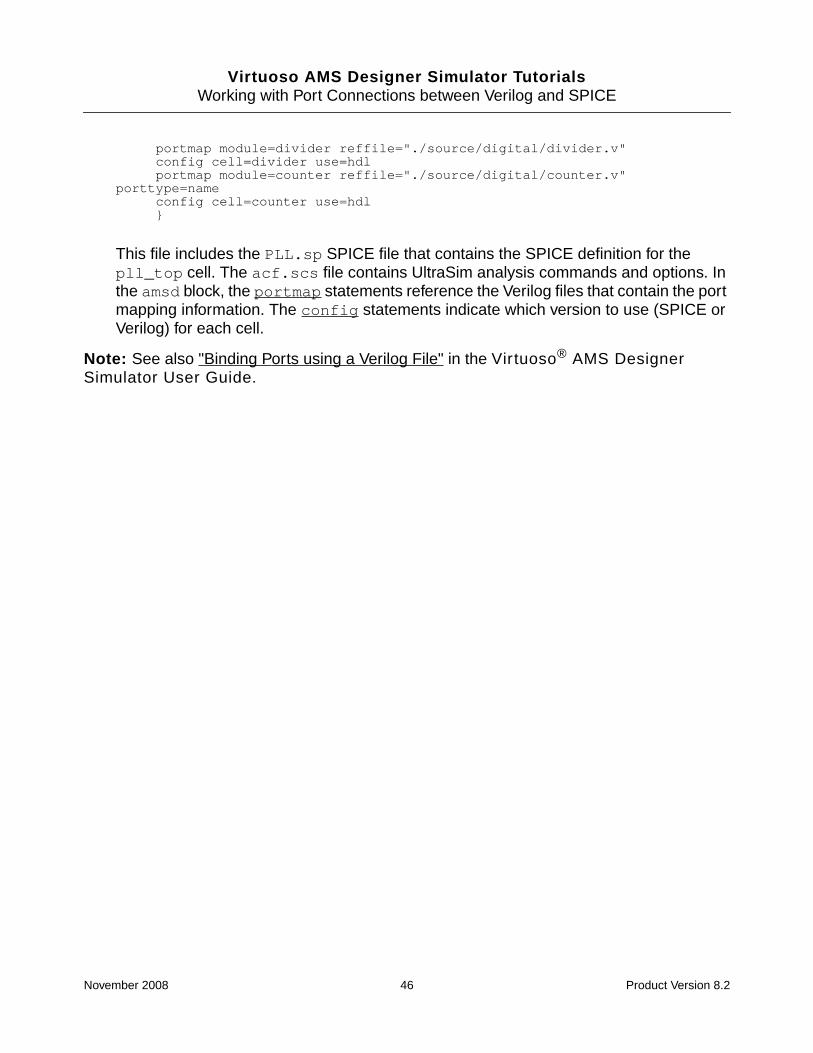
portmap module=divider reffile="./source/digital/divider.v"config cell=divider use=hdlportmap module=counter reffile="./source/digital/counter.v"
porttype=nameconfig cell=counter use=hdl}
This file includes the PLL.sp SPICE file that contains the SPICE definition for thepll_top cell. The acf.scs file contains UltraSim analysis commands and options. Inthe amsd block, the portmap statements reference the Verilog files that contain the portmapping information. The config statements indicate which version to use (SPICE orVerilog) for each cell.
Note: See also "Binding Ports using a Verilog File" in the Virtuoso® AMS DesignerSimulator User Guide.
November 2008 46 Product Version 8.2
Virtuoso AMS Designer Simulator Tutorials
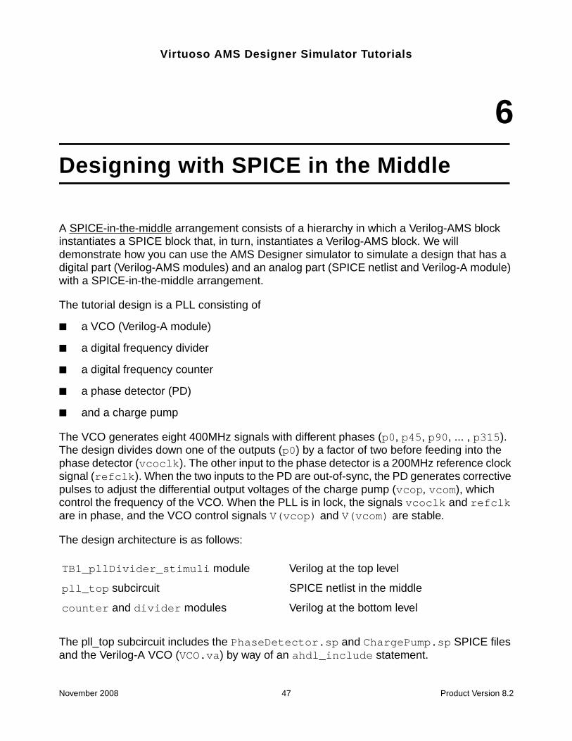
6Designing with SPICE in the Middle
A SPICE-in-the-middle arrangement consists of a hierarchy in which a Verilog-AMS blockinstantiates a SPICE block that, in turn, instantiates a Verilog-AMS block. We willdemonstrate how you can use the AMS Designer simulator to simulate a design that has adigital part (Verilog-AMS modules) and an analog part (SPICE netlist and Verilog-A module)with a SPICE-in-the-middle arrangement.
The tutorial design is a PLL consisting of
■ a VCO (Verilog-A module)
■ a digital frequency divider
■ a digital frequency counter
■ a phase detector (PD)
■ and a charge pump
The VCO generates eight 400MHz signals with different phases (p0, p45, p90, ... , p315).The design divides down one of the outputs (p0) by a factor of two before feeding into thephase detector (vcoclk). The other input to the phase detector is a 200MHz reference clocksignal (refclk). When the two inputs to the PD are out-of-sync, the PD generates correctivepulses to adjust the differential output voltages of the charge pump (vcop, vcom), whichcontrol the frequency of the VCO. When the PLL is in lock, the signals vcoclk and refclkare in phase, and the VCO control signals V(vcop) and V(vcom) are stable.
The design architecture is as follows:
The pll_top subcircuit includes the PhaseDetector.sp and ChargePump.sp SPICE filesand the Verilog-A VCO (VCO.va) by way of an ahdl_include statement.
TB1_pllDivider_stimuli module Verilog at the top level
pll_top subcircuit SPICE netlist in the middle
counter and divider modules Verilog at the bottom level
November 2008 47 Product Version 8.2
Virtuoso AMS Designer Simulator TutorialsDesigning with SPICE in the Middle
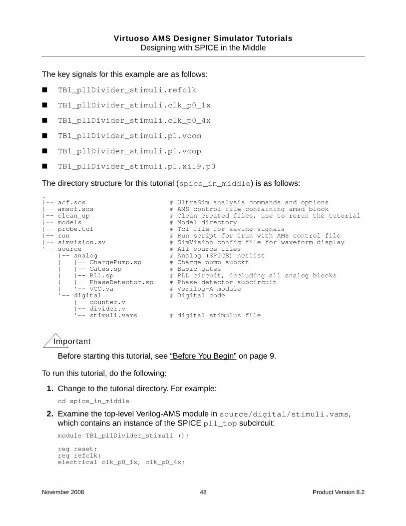
The key signals for this example are as follows:
■ TB1_pllDivider_stimuli.refclk
■ TB1_pllDivider_stimuli.clk_p0_1x
■ TB1_pllDivider_stimuli.clk_p0_4x
■ TB1_pllDivider_stimuli.p1.vcom
■ TB1_pllDivider_stimuli.p1.vcop
■ TB1_pllDivider_stimuli.p1.xi19.p0
The directory structure for this tutorial (spice_in_middle) is as follows:
.|-- acf.scs # UltraSim analysis commands and options|-- amscf.scs # AMS control file containing amsd block|-- clean_up # Clean created files, use to rerun the tutorial|-- models # Model directory|-- probe.tcl # Tcl file for saving signals|-- run # Run script for irun with AMS control file|-- simvision.sv # SimVision config file for waveform display'-- source # All source files
|-- analog # Analog (SPICE) netlist| |-- ChargePump.sp # Charge pump subckt| |-- Gates.sp # Basic gates| |-- PLL.sp # PLL circuit, including all analog blocks| |-- PhaseDetector.sp # Phase detector subcircuit| '-- VCO.va # Verilog-A module'-- digital # Digital code
|-- counter.v|-- divider.v'-- stimuli.vams # digital stimulus file
Important
Before starting this tutorial, see “Before You Begin” on page 9.
To run this tutorial, do the following:
1. Change to the tutorial directory. For example:
cd spice_in_middle
2. Examine the top-level Verilog-AMS module in source/digital/stimuli.vams,which contains an instance of the SPICE pll_top subcircuit:
module TB1_pllDivider_stimuli ();
reg reset;reg refclk;electrical clk_p0_1x, clk_p0_4x;
November 2008 48 Product Version 8.2
Virtuoso AMS Designer Simulator TutorialsDesigning with SPICE in the Middle
initial beginreset=1;#50 reset=0;
end
initial beginrefclk=0;#200 refclk=1;
end
always #2500 refclk=~refclk;
pll_top p1(refclk, reset, clk_p0_1x, clk_p0_4x);
endmodule
3. Examine source/analog/PLL.sp, which contains dummy SPICE subcircuitdefinitions for divider and for counter. The software uses these definitions whengenerating the port-bind files for the AMS Designer simulator.
.subckt divider result_0 result_1 clock asynch_reset
.ends divider
.subckt counter asynch_reset clock out[2] out[1] out[0]
.ends counter
4. Further examine source/analog/PLL.sp, which also contains a SPICE subcircuitdefinition for plldivider_g17. This subcircuit definition contains instances of Verilogmodules counter and divider (whose source files are in source/digital). Thepll_top SPICE subcircuit definition contains an instance of the plldivider_g17subcircuit:
...
.subckt plldivider_g17 clk_p0_1x clk_p0_4x ibias p0 p45 p90 p135 p180 p225+p270 p315 refclk reset vcoclk vcom vcop inh_setic0 inh_vdd inh_vss...xi116 reset vcoclk clock_2 clock_1 clock_0 counter...xi20 vcoclk net036 p0 reset divider....subckt pll_top refclk reset clk_p0_1x clk_p0_4x* xi22 refclk reset sub2xi19 clk_p0_1x clk_p0_4x ibias net038 net034 net027 net033 net026 net032+net025 net031 refclk reset net030 vcom vcop setic0! vdd! 0 plldivider_g17...
The SPICE-in-the-middle arrangement consists of the stimuli.vams Verilog-AMS filethat instatiates the pll_top SPICE subcircuit that, in turn, instantiates theplldivider_g17 subcircuit that, in turn, instantiates two Verilog modules: counterand divider.
November 2008 49 Product Version 8.2
Virtuoso AMS Designer Simulator TutorialsDesigning with SPICE in the Middle
5. Examine the config statements in the amsd block in the amscf.scs file:
***********include "./source/analog/PLL.sp"include "./models/resistor.scs" section=resinclude "./models/diode.scs" section=dioinclude "./models/pmos1.scs" section=nominclude "./models/nmos1.scs" section=nominclude "acf.scs"
amsd{ie vsup=1.8portmap subckt=pll_topconfig cell=pll_top use=spiceportmap module=divider reffile="./source/digital/divider.v"config cell=divider use=hdlportmap module=counter reffile="./source/digital/counter.v"config cell=counter use=hdl
}
These statements specify which version to use (SPICE or Verilog) for each cell.
6. To run the tutorial, use the run script:
./run
7. (Optional) To clean up simulation-generated files, run the clean_up script:
./clean_up
November 2008 50 Product Version 8.2
Virtuoso AMS Designer Simulator Tutorials
7Using AMS Keywords
The Virtuoso AMS Designer simulator provides a mechanism for specifying the active set ofkeywords when mixing Verilog-AMS and Verilog languages together in the same design.Using this mechanism, you can avoid keyword clashes that might otherwise occur when legalwire names in the Verilog language turn out to be identifiers or keywords in the Verilog-AMSlanguage. For example, the port name sin in Verilog might clash with the sin sinusoidalfunction name in Verilog-AMS unless you select a set of active keywords to prevent this clash.
Here is how it works:
1. Use the `begin_keywords directive in the Verilog file before the module that uses theidentifier or keyword that might clash to specify the active set of keywords. For example:
`begin_keywords "1364-2001"
This string specifies the Verilog 2001 set of keywords. Using this setting, the parser doesnot recognize Verilog-AMS keywords such as sin, cos, and discipline as keywords.
2. Use the `end_keywords directive after the Verilog module to reset the keyword list tocontain Verilog-AMS keywords.
For more information about these directives, see “Specifying Which Reserved Keyword Listto Use“ in the Cadence Verilog-AMS Language Reference.
This tutorial example takes about 10 minutes to complete.
The tutorial example is a simple design that contains a Verilog (digital) module and aVerilog-AMS module. The design files and directory structure looks like this:
.|-- acf.scs # Analog control file, including simulator options|-- amscf.scs # AMS control file|-- clean_up # Clean created files|-- run # Run script'-- source # Includes digital source files
|-- ams_module.vams|-- dig_module.vams'-- top.v
November 2008 51 Product Version 8.2
Virtuoso AMS Designer Simulator TutorialsUsing AMS Keywords
Important
Before starting this tutorial, see “Before You Begin” on page 9.
To run this tutorial, do the following:
1. Change to the tutorial directory. For example:
cd amsKeywords
2. Use the run script:
./run
The compilation fails with error messages:
file: ./source/dig_module.vamsparameter sin = "hello"; // uses an AMS keyword as an identifier!
|ncvlog: *E,FNDKWD (./source/dig_module.vams,5|12): A Verilog keyword was foundwhere an identifier was expected.
$strobe("%s",sin);|
ncvlog: *E,EXPLPA (./source/dig_module.vams,7|22): expecting a leftparenthesis ('(') [4.2(AMSLRM)].
module worklib.digital_module:vamserrors: 2, warnings: 0
3. Run the clean-up script to remove the generated files:
./clean_up
4. Edit source/dig_module.vams to remove the comment delimiter (//) from thebeginning of lines 2 and 12 so that the `begin_keywords and `end_keywordsdirectives are active:
`begin_keywords "1364-2001"
module digital_module;parameter sin = "hello"; // uses an AMS keyword as an identifier!initial begin
$strobe("%s",sin);endendmodule
`end_keywords
5. Save and close the file.
The parser will recognize only the subset of Verilog-AMS keywords that are part of the1364-2001 standard as keywords.
6. Use the run script again:
./run
November 2008 52 Product Version 8.2

Virtuoso AMS Designer Simulator TutorialsUsing AMS Keywords
There are no errors.
7. (Optional) Run the clean-up script to remove generated files:
./clean_up
November 2008 53 Product Version 8.2

Virtuoso AMS Designer Simulator TutorialsUsing AMS Keywords
November 2008 54 Product Version 8.2
Virtuoso AMS Designer Simulator Tutorials
8Using the Save-and-Restart Feature ofthe AMS Designer Simulator
AMS-Spectre means the Virtuoso® AMS Designer simulator using the Spectre solver.AMS-UltraSim means the Virtuoso AMS Designer simulator using the UltraSim solver.
Note: The estimated time to complete this tutorial is 1.5 hours.
You can use the save-and-restart feature of the Virtuoso® AMS Designer simulator (bothAMS-Spectre and AMS-UltraSim) to save the simulation database at a specific time point anduse that saved database to restart the simulation from that same time point. In particular, thesave-and-restart feature lets you
■ Achieve maximum simulation speed by simulating only the portion of time that requiresa highly accurate simulation mode (for example, simulating a PLL locking process inaccurate mode and then switching to a higher speed mode once the PLL is locked)
■ Perform what-if analyses on problematic sections of a design
■ Test circuits that are only semi-functional using an abstract model for unimplementedcapabilities
■ Save and restart for “rainy days” such as unexpected simulation crashes
You can save time by saving snapshots during a long simulation run (such as a full-chipdesign that might take days, or even weeks) so that you do not need to rerun the simulationfrom the beginning (to support any special debugging/analysis purposes you might have orin case of any mishaps that might occur), especially prior to tape-out.
Important
If you want to use save-and-restart with AMS-Spectre, you must be using thesimulation front end (SFE) parser. You can use save-and-restart either in non-interactive mode or in Tcl mode.
Running AMS-UltraSim, you can save either in non-interactive (command-line)mode or in Tcl mode, but you can restart only in command-line mode.
November 2008 55 Product Version 8.2
Virtuoso AMS Designer Simulator TutorialsUsing the Save-and-Restart Feature of the AMS Designer Simulator
See the following topics for tutorial details:
Important
Before starting this tutorial, see “Before You Begin” on page 9.
■ Save-and-Restart Use Models on page 57
■ Test Case Description on page 57
■ Using Save-and-Restart in AMS-Spectre on page 58
■ Using Save-and-Restart in AMS-UltraSim on page 61
4.2.2 Options in irun to support save/restart
* -snapshot <snapshot_name> : to save snapshot after elaboration at command-line
* -r <snapshot_name> : Force simulation using snapshot you saved before(fromcommand-line or tcl)
* -R : Simulate using last snapshot generated
Basically you can use irun -R -r <snapshot_name> <other options> to restart from iruncommand line, for both AMS-Spectre and AMS-Ultrasim.
Please note at restart you can modify some irun simulation command options, insteadof adding only -R -r <snapshot_name> options.
tagit:make sure above info is included
November 2008 56 Product Version 8.2
Virtuoso AMS Designer Simulator TutorialsUsing the Save-and-Restart Feature of the AMS Designer Simulator
Save-and-Restart Use Models
The most common use models for save-and-restart are
■ Running AMS-Spectre, save a snapshot of a simulation in Tcl and restart in Tcl mode orin command-line mode after making changes in the analog control file to simulationparameters such as reltol or abstol that do not affect the circuit topology
■ Running AMS-UltraSim, you can save a snapshot in Tcl mode, but you can restart onlyin command-line mode
Test Case Description
The design in this tutorial is an oscillator circuit composed of AC-coupled varactors. Itproduces an oscillated clock (4 GHz) which is then modulated by a digital clock (500 KHz).The top-level DUT is a SPICE block and the top-level test bench is a Verilog-AMS module.You will run this example using both AMS-Spectre and AMS-UltraSim.
The test case file/directory structure is as follows:
.|-- amsControl_tran.scs # analog control file for UltraSim/AMS-Spectre|-- amsControl_tran.tcl # Tcl script for save/restart|-- amsControl_tran_spectre1.scs # analog control file for AMS-Spectre
with changed options|-- amscf_tran.scs # AMS control file|-- bsim.mos # original transistor models|-- bsim_new.mos # transistor models for AMS save/restart|-- clean_up # clean-up script|-- moscap.va # MOS capacitor Verilog-A model|-- multiplier.va # multiplier Verilog-A model|-- run # run script|-- run_amss # run script for AMS-Spectre|-- run_amss_restart # run script for AMS-Spectre with restart|-- run_amsu # run script for AMS-UltraSim|-- run_amsu_restart # run script for AMS-UltraSim with restart|-- test.v # Verilog test bench (top level)|-- test.vams # Verilog-AMS test bench (top level)`-- vco.scs # SPICE on top DUT
November 2008 57 Product Version 8.2
Virtuoso AMS Designer Simulator TutorialsUsing the Save-and-Restart Feature of the AMS Designer Simulator
Using Save-and-Restart in AMS-Spectre
To run the tutorial using AMS-Spectre, do the following:
1. Change to the tutorial directory. For example:
cd amsd_saverestart
2. Examine the top-level Verilog-AMS testbench in test.vams:
`timescale 1us / 100fs`include "disciplines.vams"
module test();
electrical vp, vn, sub;ground sub;reg clk;wire vin;
initial clk=1;
always #1 clk=~clk;
assign vin=clk;top top1 (vin, vp, vn, sub);
endmodule
This testbench generates a 500 KHz baseband clock.
3. Examine the top-level DUT in vco.scs. The top-level SPICE subcircuit, top, containsinstances of a Verilog-A MOS capacitor (rfCap, in the genericvar subcircuitdefinition), a Verilog-A multiplier (multiplier), and some SPICE components.The ahdl_include statements include the Verilog-A models:
simulator lang=spectreahdl_include "moscap.va"ahdl_include "multiplier.va"
4. Examine the analog control file, amsControl_tran.scs, which contains simulationanalysis commands and options settings, such as:
tight options reltol=1.0e-6
5. Run the script that references the AMS control file that includesamsControl_tran.scs (amscf_tran.scs):
./run_amss
The simulation stops at the Tcl ncsim> prompt.
6. Type the following run command and wait until it finishes:
ncsim> run 1us
7. Type the following save command:
November 2008 58 Product Version 8.2
Virtuoso AMS Designer Simulator TutorialsUsing the Save-and-Restart Feature of the AMS Designer Simulator
ncsim> save amss1us
A confirmation message appears:
Saved snapshop worklib.amss1us:vams
8. Type the following ls command:
ncsim> ls -a INCA_libs/worklib
A new .pkl file appears:
.worklib.amss1us.vams.lnx86.166.pkl
9. Type the following run command and watch while the simulation runs until 3 µs:
ncsim> run 2us
10. Type the following restart command:
ncsim> restart amss1us
A confirmation message appears:
Loaded snapshot worklib.amss1us:vams
11. Type the time command to check the current run time:
ncsim> time1 US
The program confirms that the current run time is 1 µs.
12. Type the following run command and wait until it finishes:
ncsim> run 1.5us
The simulation reaches 2.5 µs: save-and-restart worked.
13. Type the following run command:
ncsim> run
The simulation runs until 4 µs and stops because that is the stop time specified in theanalog control file.
14. Type the exit command:
ncsim> exit
15. Start SimVision:
simvision &
16. Choose File – Open Database to load and review the following waveform files in thewaves_tran.shm directory:
❑ waves_tran.trn
The simulation duration in this case is 1 µs which matches the snapshot time point.
November 2008 59 Product Version 8.2
Virtuoso AMS Designer Simulator TutorialsUsing the Save-and-Restart Feature of the AMS Designer Simulator
❑ waves_tran-1.trn
❑ waves_tran-2.trn
17. In SimVison, choose File – Exit SimVision.
18. Save waves_tran.shm to a different directory for later comparison.
19. Examine amsControl_tran_spectre1.scs.
reltol is 1e-4 instead of 1e-6 (which was its value in amsControl_tran.scs).
You will use this analog control file to restart the simulation.
20. Examine the restart run script, run_amss_restart:
irun \
amscf_tran_spectre1.scs \ AMS control file that referencesamsControl_tran_spectre1.scsand bsim_new.mos instead ofamsControl_tran.scs and bsim.mos
-input amsControl_tran.tcl \ Use the same Tcl script-simcompat spectre \ Use Spectre-compatible simulation values-R \ Simulate using a snapshot in the
INCA_libs/worklib directory-r amss1us Load the saved snapshot
21. Run this script to restart the simulation using the saved snapshot, amss1us:
./run_amss_restart
The simulation restarts from the snapshot time point, 1 µs.
22. At the Tcl prompt, type the following run command:
ncsim> run 1.5us
The simulation stops at 2.5 µs. Note the changed value for reltol.
23. Type the run command and wait until it finishes:
ncsim> run
24. Exit the simulation:
ncsim> exit
25. Choose File – Open Database to load and compare the waveform files in thewaves_tran.shm directory with the previous waveform files.
26. Run the clean-up script:
./clean_up
November 2008 60 Product Version 8.2
Virtuoso AMS Designer Simulator TutorialsUsing the Save-and-Restart Feature of the AMS Designer Simulator
Using Save-and-Restart in AMS-UltraSim
To run the tutorial using AMS-UltraSim, do the following:
1. Make sure you are in the tutorial amsd_saverestart tutorial directory.
2. Examine the run_amsu script and make sure you see -amsf (enables UltraSim) on theirun command.
irun -amsf ...
3. Examine the amsControl_tran.scs control file to view this UltraSim option:
*UltraSim: .usim_opt sim_mode=a speed=1
We set speed to 1 for higher accuracy.
4. Run the script:
./run_amsu
5. At the Tcl prompt, type the following run command:
ncsim> run 1.5us
6. To save the database, type the following save command:
ncsim> save amsu1p5usSaving Simulation state at 1.5e-06 sec
Save operation completes.
Saved snapshot worklib.amsu1p5us:vams
7. Type the run command:
ncsim> run
8. Exit the simulation:
ncsim> exit
9. Start SimVision:
simvision &
10. Choose File – Open Database to load and examine the following waveform files:
❑ waves_tran.trn
❑ waves_tran-1.trn
November 2008 61 Product Version 8.2
Virtuoso AMS Designer Simulator TutorialsUsing the Save-and-Restart Feature of the AMS Designer Simulator
11. Examine the restart run script, run_amsu_restart:
12. Run this script to restart the simulation using the saved snapshot, amsu1p5us:
./run_amsu_restart
The simulation restarts from the snapshot time point, 1.5 µs.
13. At the Tcl prompt, type the following run command:
ncsim> run 1us
The simulation runs until 2.5 µs.
14. Type the run command:
ncsim> run
15. Exit the simulation:
ncsim> exit
16. Start SimVision and compare these waveform results with the AMS-Spectre waveformresults.
irun \
amscf_tran.scs \ AMS control file
-input amsControl_tran.tcl \ Tcl probes
-simcompat spectre \ Spectre simulation compatibility
-R \ Simulate using a snapshot in theINCA_libs/worklib directory
-r amsu1p5us Load the saved snapshot
November 2008 62 Product Version 8.2
Virtuoso AMS Designer Simulator Tutorials
9Performing Envelope Analysis UsingAMS-Spectre
Note: AMS-Spectre means the Virtuoso® AMS Designer simulator using the Spectre solver.
RF designs are complex high-speed designs widely used in wireless systems. Some RFdesigns such as modulation systems have a very high carrier frequency along with one ormore baseband frequencies that are orders of magnitude lower. It is difficult to simulate usingtraditional transient analysis because the simulator must use a very tiny time step toaccommodate the high carrier frequency thus requiring a huge number of time steps tosimulate.
In this tutorial, you will run envelope simulation for RF circuits. Envelope analysis is asimulation technique developed to reduce the large number of time steps and highcomputational costs associated with conventional transient RF analysis. During envelopeanalysis, the analog parts of the design are simulated with various envelope methods suchas FM envelope for frequency-modulated sources, autonomous envelope for oscillators,harmonic balance envelope, shooting Newton envelope, and multi-carrier envelope. Thedigital parts are handled entirely by the digital solver. For each envelope step, the envelopesolver skips as many high-frequency cycles as possible while keeping fine accuracy within anallowed range. Digital and analog parts of the design are synchronized through A/D and D/Aevents at the next analog solution point.
Envelope simulation is most efficient for RF circuits with modulation frequencies that areorders of magnitude lower than the carrier frequency. For example, circuits that have a clockas the only fast-varying signal in addition to other input signals that have a spectrum with afrequency range that is orders of magnitude lower than the clock frequency.
In general, envelope simulation is not intended for circuits working with multiple carriers(fundamentals). However, you can use it for specific classes of circuits that operate withmultiple, proportionate fundamentals. In this case, you use the greatest commondenominator of all fundamental frequencies as the clock frequency.
Note: The Virtuoso AMS Designer envelope simulation supports only SPICE and analogsimulation modes. You can simulate circuits with amplitude modulation signals with someminor frequency and phase modulations.
November 2008 63 Product Version 8.2
Virtuoso AMS Designer Simulator TutorialsPerforming Envelope Analysis Using AMS-Spectre
In this tutorial, you will run envelope simulation using the AMS-Spectre simulator. There aretwo tutorial modules:
■ A simple digital modulator/demodulator (non-autonomous)
■ An AC-coupled oscillator (autonomous)
See the following topics for tutorial details:
Important
Before starting this tutorial, see “Before You Begin” on page 9.
■ Envelope Analysis Syntax and Parameters on page 65
■ Tutorial Module 1: Envelope Analysis for Digital Modulator/Demodulator on page 67
■ Tutorial Module 2: Envelope Analysis for Oscillator on page 70
November 2008 64 Product Version 8.2
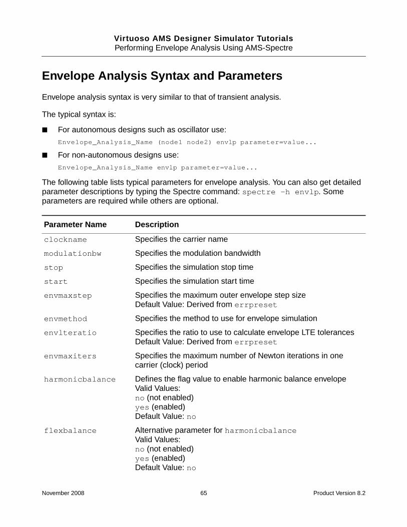
Virtuoso AMS Designer Simulator TutorialsPerforming Envelope Analysis Using AMS-Spectre
Envelope Analysis Syntax and Parameters
Envelope analysis syntax is very similar to that of transient analysis.
The typical syntax is:
■ For autonomous designs such as oscillator use:
Envelope_Analysis_Name (node1 node2) envlp parameter=value...
■ For non-autonomous designs use:
Envelope_Analysis_Name envlp parameter=value...
The following table lists typical parameters for envelope analysis. You can also get detailedparameter descriptions by typing the Spectre command: spectre -h envlp. Someparameters are required while others are optional.
Parameter Name Description
clockname Specifies the carrier name
modulationbw Specifies the modulation bandwidth
stop Specifies the simulation stop time
start Specifies the simulation start time
envmaxstep Specifies the maximum outer envelope step sizeDefault Value: Derived from errpreset
envmethod Specifies the method to use for envelope simulation
envlteratio Specifies the ratio to use to calculate envelope LTE tolerancesDefault Value: Derived from errpreset
envmaxiters Specifies the maximum number of Newton iterations in onecarrier (clock) period
harmonicbalance Defines the flag value to enable harmonic balance envelopeValid Values:no (not enabled)yes (enabled)Default Value: no
flexbalance Alternative parameter for harmonicbalanceValid Values:no (not enabled)yes (enabled)Default Value: no
November 2008 65 Product Version 8.2
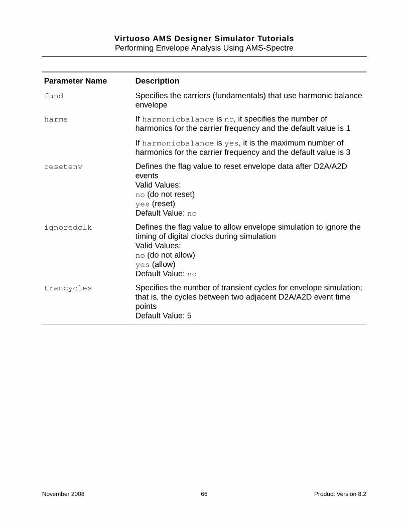
Virtuoso AMS Designer Simulator TutorialsPerforming Envelope Analysis Using AMS-Spectre
fund Specifies the carriers (fundamentals) that use harmonic balanceenvelope
harms If harmonicbalance is no, it specifies the number ofharmonics for the carrier frequency and the default value is 1
If harmonicbalance is yes, it is the maximum number ofharmonics for the carrier frequency and the default value is 3
resetenv Defines the flag value to reset envelope data after D2A/A2DeventsValid Values:no (do not reset)yes (reset)Default Value: no
ignoredclk Defines the flag value to allow envelope simulation to ignore thetiming of digital clocks during simulationValid Values:no (do not allow)yes (allow)Default Value: no
trancycles Specifies the number of transient cycles for envelope simulation;that is, the cycles between two adjacent D2A/A2D event timepointsDefault Value: 5
Parameter Name Description
November 2008 66 Product Version 8.2
Virtuoso AMS Designer Simulator TutorialsPerforming Envelope Analysis Using AMS-Spectre
Tutorial Module 1: Envelope Analysis for DigitalModulator/Demodulator
The design you will simulate in this module is a digital modulator/demodulator. The DUT hasSPICE on top and consists of five major Verilog-A blocks, an adder, three multipliers, and ademodulator. There is a Verilog-AMS test bench on top that generates the 50 KHz basebandclock for the DUT. I and Q signals (generated from data file) are 2 GHz sinusoidal carriersignals with 90 degree phase apart from each other. The adder produces the sum of I and Qsignal. The output signal then feeds into the multiplier for modulation. Then the output signalis passed to the demodulator. Note that the carrier signal is 2 GHz while the baseband signalis 50 KHz, orders of magnitude lower than the carrier frequency. In other words, themodulation ratio is 50 KHz/2 GHz=2.5e-5, much less than 1.0. It is a suitable example forenvelope analysis.
The file/directory structure for Module 1 is as follows (underamss_envelope/simpDM_hbenv):
.|-- adder.va # adder Verilog-A model|-- amsControl_env.scs # analog control file for env analysis|-- amsControl_env.tcl # Tcl script saving signals for envelope analysis|-- amsControl_tran.scs # analog control file for tran analysis|-- amsControl_tran.tcl # Tcl script saving signals for transient analysis|-- amscf_env.scs # AMS control file for env analysis|-- amscf_tran.scs # AMS control file for tran analysis|-- clean_up # clean-up script|-- datafile # data file directory|-- demodulator.va # demodulator Verilog-A model|-- multiplier.va # multiplier Verilog-A model|-- run_env # run script for envelope analysis|-- run_tran # run script for transient analysis|-- simpDM.scs # SPICE subcircuit file for digital modulator'-- test.vams # Verilog-AMS testbench
Note: There are two sets of run scripts (run_*), analog control files (amsControl_*.scs),and Tcl scripts (amsControl_*.tcl): one for transient analysis (*_tran) and one forenvelope analysis (*_env). Simulation time is 60 µs.
To run the tutorial, do the following in the amss_envelope/simpDM_hbenv directory:
1. Examine module test in test.vams and notice that the testbench generates a 50 KHzbaseband clock (period=20us):
module test();electrical Vmout, vout, sub;ground sub;reg clk;wire vin;initial clk=0;always #1 clk=~clk;assign vin=clk;
November 2008 67 Product Version 8.2
Virtuoso AMS Designer Simulator TutorialsPerforming Envelope Analysis Using AMS-Spectre
top top1 (vin, vout, Vmout, sub);endmodule
2. Examine the subcircuit definition for the top-level DUT (top) in simpDM.scs, whichcontains five Verilog-A blocks: three multipliers, one adder, and one demodulator:
simulator lang=spectreahdl_include "multiplier.va"ahdl_include "adder.va"ahdl_include "demodulator.va"parameters plo=-10 fcar=2G
subckt top vin vout vmout subR2 (MixOut 0) resistor r=50R9 (net22 0) resistor r=50R8 (net20 0) resistor r=50R10 (net9 0) resistor r=50R3 (net12 0) resistor r=50I13 (net9 net20 net16) multiplierI16 (net12 net22 net14) multiplierI11 (net14 net16 MixOut) adderPORT3 (net12 0) vsource type=sine freq=fcar ampl=0.5e-3 fundname="fff"PORT0 (net20 0) vsource type=pwl phase=0 fundname="IIN" \
file="./datafile/i_data.ascsig"PORT1 (net22 0) vsource type=pwl phase=0 fundname="QIN" \
file="./datafile/q_data.ascsig"PORT2 (net9 0) vsource type=sine freq=fcar ampl=0.5e-3 sinephase=90 \
fundname="fff"
I1 (MixOut vin vmout) multiplierI2 (vmout vdif vout) demodulator w=6.28*2.0e9R1 (vout sub) resistor r=50RR (vdif sub) resistor r=50ends top
3. Use the transient run script to run the transient analysis:
./run_tran
When the simulation finishes, note the run time.
Intrinsic tran analysis time = 180.72 s.
4. Examine the envelope analysis parameter settings in amsControl_env.scs:
envlp envlp clockname="fff" stop=60u maxstep=0.2ns annotate=status tstab=15nflexbalance=yes trancycles=10
5. Use the envelope analysis run script to run the envelope analysis:
./run_env
Pay attention to the log messages during the simulation:
Envelope Following Analysis `envlp': time = (0 s -> 60 us)**********************************************************Onset of periodicity = 500 psClock period = 500 psInital transient integration from 0 s to 15 ns
November 2008 68 Product Version 8.2
Virtuoso AMS Designer Simulator TutorialsPerforming Envelope Analysis Using AMS-Spectre
Envelope Analysis Using Harmonic Balance ...EnvStepIndex = 1, envTime = 15.5 ns, completed = (25.8 m%)EnvStepIndex = 2, envTime = 16 ns, completed = (26.7 m%)...
envTime indicates envelope analysis time points. The intervals (time steps) betweentwo adjacent envTime points are changing all the time as a result of digital events, inputcontrol signal changes, and so on.
Pay attention to the simulation summary when it finishes.
Total clock cycles: 119969, skipped cycles: 119663, speed-up factor: 377Done with the envelope-following analysis.Clean up envelope following analysis.Total time required for envlp analysis `envlp' was 46.63 s
Note that 90% of the clock cycles have been skipped. As a result, the envelope analysistime is three-to-five times less than that of the transient analysis. The speed-up factorapplies only to analog parts.
6. Start SimVision:
simvision &
7. Choose File – Open Database to load the waveform file from the waves_env.shmdirectory. You can also overlay it with the transient waveform and compare the twowaveforms.
8. Run the clean-up script:
./clean_up
You have completed Module 1.
November 2008 69 Product Version 8.2
Virtuoso AMS Designer Simulator TutorialsPerforming Envelope Analysis Using AMS-Spectre
Tutorial Module 2: Envelope Analysis for Oscillator
The design you are going to simulate in this module is an Oscillator. The top-level DUT is aSPICE block containing three major blocks: a varacator (SPICE), a moscap (Verilog-A), anda multiplier (Verilog-A). It is instantiated in a Verilog AMS test bench which generates a500 KHz baseband clock. The carrier frequency is the oscillator frequency, 4 GHz.Nevertheless, it is unknown at the beginning before the oscillator is locked.
You should use the envelope analysis command for autonomous devices in this module.
The simulation time is 4us.
The file/directory structure for Module 2 is as follows (under amss_envelope/osc_hb):
.|-- amsControl_env.scs # analog control file for env analysis|-- amsControl_env.tcl # Tcl script saving signals for envelope analysis|-- amsControl_tran.scs # analog control file for tran analysis|-- amsControl_tran.tcl # Tcl script saving signals for transient analysis|-- amscf_env.scs # AMS control file for env analysis|-- amscf_tran.scs # AMS control file for tran analysis|-- clean_up # clean-up script|-- moscap.va # MOS capacitor Verilog-A model|-- multiplier.va # multiplier Verilog-A model|-- run_env # run script for envelope analysis|-- run_tran # run script for transient analysis|-- test.vams # Verilog-AMS testbench'-- vco.scs # top-level SPICE subcircuit definition
Note: There are two sets of run scripts (run_*), analog control files (amsControl_*.scs),and Tcl scripts (amsControl_*.tcl): one for transient analysis (*_tran) and one forenvelope analysis (*_env). Simulation time is 60 µs.
To run the simulation, do the following:
1. Change from the simpDM_hbenv directory (previous module) to the osc_hb directory:
cd ../osc_hb
2. Examine module test in test.vams and notice that the testbench generates a 500KHz baseband clock for the DUT:
module test();electrical vp, vn, sub;ground sub;reg clk;wire vin;initial clk=1;always #1 clk=~clk;assign vin=clk;top top1 (vin, vp, vn, sub);endmodule
November 2008 70 Product Version 8.2
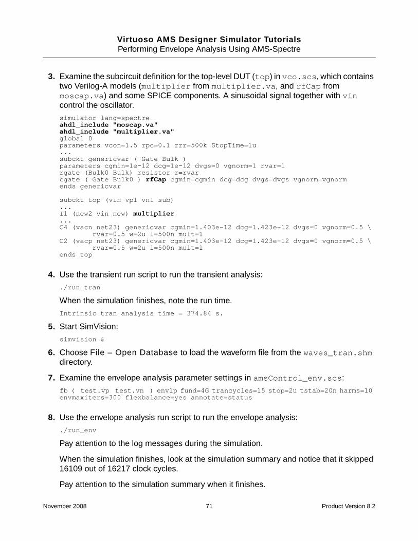
Virtuoso AMS Designer Simulator TutorialsPerforming Envelope Analysis Using AMS-Spectre
3. Examine the subcircuit definition for the top-level DUT (top) in vco.scs, which containstwo Verilog-A models (multiplier from multiplier.va, and rfCap frommoscap.va) and some SPICE components. A sinusoidal signal together with vincontrol the oscillator.
simulator lang=spectreahdl_include "moscap.va"ahdl_include "multiplier.va"global 0parameters vcon=1.5 rpc=0.1 rrr=500k StopTime=1u...subckt genericvar ( Gate Bulk )parameters cgmin=1e-12 dcg=1e-12 dvgs=0 vgnorm=1 rvar=1rgate (Bulk0 Bulk) resistor r=rvarcgate ( Gate Bulk0 ) rfCap cgmin=cgmin dcg=dcg dvgs=dvgs vgnorm=vgnormends genericvar
subckt top (vin vp1 vn1 sub)...I1 (new2 vin new) multiplier...C4 (vacn net23) genericvar cgmin=1.403e-12 dcg=1.423e-12 dvgs=0 vgnorm=0.5 \
rvar=0.5 w=2u l=500n mult=1C2 (vacp net23) genericvar cgmin=1.403e-12 dcg=1.423e-12 dvgs=0 vgnorm=0.5 \
rvar=0.5 w=2u l=500n mult=1ends top
4. Use the transient run script to run the transient analysis:
./run_tran
When the simulation finishes, note the run time.
Intrinsic tran analysis time = 374.84 s.
5. Start SimVision:
simvision &
6. Choose File – Open Database to load the waveform file from the waves_tran.shmdirectory.
7. Examine the envelope analysis parameter settings in amsControl_env.scs:
fb ( test.vp test.vn ) envlp fund=4G trancycles=15 stop=2u tstab=20n harms=10envmaxiters=300 flexbalance=yes annotate=status
8. Use the envelope analysis run script to run the envelope analysis:
./run_env
Pay attention to the log messages during the simulation.
When the simulation finishes, look at the simulation summary and notice that it skipped16109 out of 16217 clock cycles.
Pay attention to the simulation summary when it finishes.
November 2008 71 Product Version 8.2
Virtuoso AMS Designer Simulator TutorialsPerforming Envelope Analysis Using AMS-Spectre
Total clock cycles: 8072, skipped cycles: 8018, speed-up factor: 128Done with the envelope-following analysis.Clean up envelope following analysis.Total time required for envlp analysis `fb' was 14.78 s
The analog speed-up factor is 128. The run time is 25 times less for the envelopeanalysis than for the transient analysis.
9. Start SimVision:
simvision &
10. Choose File – Open Database to load the waveform file from the waves_env.shmdirectory. You can also overlay it with the transient waveform and compare the twowaveforms. The oscillation in the envelope analysis is much sparser than that in thetransient analysis because of the huge amount of cycle skipping.
11. Run the clean-up script:
./clean_up
November 2008 72 Product Version 8.2
Virtuoso AMS Designer Simulator Tutorials
10Performing Fast Envelope Analysis UsingAMS-UltraSim
Note: AMS-UltraSim means the Virtuoso® AMS Designer simulator using the UltraSimsolver. See also “Before You Begin” on page 9.
In general, RF circuits have a modulation bandwidth orders of magnitude lower than the clockfrequency of the circuit; for example, a circuit where the clock frequency is the only fast-varying signal and where the other input signals have a frequency range spectrum orders ofmagnitude lower than the clock frequency. The conventional transient analysis is inefficientfor RF circuit simulation because the widely-separated spectral components require timedurations to depend on the slow baseband signals, while time steps depend on the fast carriersignals. This condition results in too many time steps and very expensive computationalcosts.
Fast envelope analysis is an efficient analysis for RF circuits because it skips many timepoints in a clock cycle to reduce both the large number of time steps and the highcomputational costs. You can perform a fast envelope analysis globally (for the entire circuit)or locally (for a subcircuit or a subcircuit instance). Local fast envelope analysis provides youwith the flexibility to designate the part of the circuit with high frequency signals for fastenvelope analysis.
In general, you can set up a fast envelope analysis using the AMS Designer simulator withthe UltraSim solver (AMS-UltraSim) by adding some extra parameters to the transientanalysis setup. For example, examine the differences between fastenv/top_tran.scsand fastenv/top_fenv.scs, and notice the following parameters for envelope analysis(in top_fenv.scs):
.usim_opt sim_mode=s speed=1 env_clockf=2.45Ghz env_maxnstep=10
For information about these parameters (and others), see “Fast Envelope Simulation for RFCircuits“ in the Virtuoso UltraSim Simulator User Guide. See also “Details about FastEnvelope Support” in the Virtuoso AMS Designer Simulator User Guide.
November 2008 73 Product Version 8.2
Virtuoso AMS Designer Simulator TutorialsPerforming Fast Envelope Analysis Using AMS-UltraSim
Design Information
This tutorial design is an RF circuit that includes a transmitter and a receiver (SPICE netlists)and ADC & DAC behavioral modules (Verilog-AMS).
The file/directory structure for this tutorial is as follows (under fastenv):
.|-- amscf_fenv.scs # AMS control file for fast envelope analysis|-- amscf_tran.scs # AMS control file for transient analysis|-- clean_up # clean-up script|-- comparison.sv # SimVision file for waveform comparison|-- dout.vec # vector file for simulation read-in|-- file_list # list of files to compile|-- models # model files| |-- spectre| '-- vlc_models|-- probe_fenv.tcl # Tcl script for fast envelope analysis|-- probe_tran.tcl # Tcl script for transient analysis|-- run_fenv # run script for fast envelope analysis|-- run_tran # run script for transient analysis|-- source # source files| |-- dcocip.s # S parameters| |-- I_in.vec # digital stimulus| '-- analog # analog netlists and Verilog-A modules| | |-- balun.va| | |-- balun_wlan.va| | |-- receiver.scs| | '-- transmitter.scs| |-- connectmodule # 3.3V connect modules and connect rules| | |-- Bidir_2.vams| | |-- ConnRules3_3.vams| | |-- E2L_2.vams| | |-- L2E_2.vams| '-- digital # Verilog source| |-- adc.vams| |-- adc_8bit_ideal.vams| |-- amplifier.vams| |-- checkSign.vams| |-- dac.vams| |-- dac_8bit_ideal.vams| |-- mdelay.vams| |-- testbench.vams| '-- testbench_i.vams|-- top_fenv.scs # analog control file for envelope analysis'-- top_tran.scs # analog control file for transient analysis
November 2008 74 Product Version 8.2
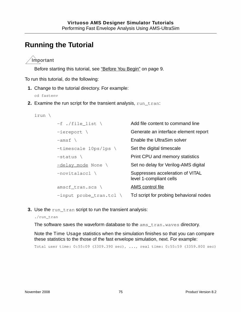
Virtuoso AMS Designer Simulator TutorialsPerforming Fast Envelope Analysis Using AMS-UltraSim
Running the Tutorial
Important
Before starting this tutorial, see “Before You Begin” on page 9.
To run this tutorial, do the following:
1. Change to the tutorial directory. For example:
cd fastenv
2. Examine the run script for the transient analysis, run_tran:
3. Use the run_tran script to run the transient analysis:
./run_tran
The software saves the waveform database to the ams_tran.waves directory.
Note the Time Usage statistics when the simulation finishes so that you can comparethese statistics to the those of the fast envelope simulation, next. For example:
Total user time: 0:55:09 (3309.390 sec), ..., real time: 0:55:59 (3359.800 sec)
irun \
-f ./file_list \ Add file content to command line
-iereport \ Generate an interface element report
-amsf \ Enable the UltraSim solver
-timescale 10ps/1ps \ Set the digital timescale
-status \ Print CPU and memory statistics
-delay_mode None \ Set no delay for Verilog-AMS digital
-novitalaccl \ Suppresses acceleration of VITALlevel 1-compliant cells
amscf_tran.scs \ AMS control file
-input probe_tran.tcl \ Tcl script for probing behavioral nodes
November 2008 75 Product Version 8.2
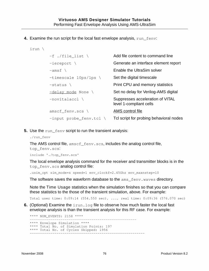
Virtuoso AMS Designer Simulator TutorialsPerforming Fast Envelope Analysis Using AMS-UltraSim
4. Examine the run script for the local fast envelope analysis, run_fenv:
5. Use the run_fenv script to run the transient analysis:
./run_fenv
The AMS control file, amscf_fenv.scs, includes the analog control file,top_fenv.scs:
include "./top_fenv.scs"
The local envelope analysis command for the receiver and transmitter blocks is in thetop_fenv.scs analog control file:
.usim_opt sim_mode=s speed=1 env_clockf=2.45Ghz env_maxnstep=10
The software saves the waveform database to the ams_fenv.waves directory.
Note the Time Usage statistics when the simulation finishes so that you can comparethese statistics to the those of the transient simulation, above. For example:
Total user time: 0:09:14 (554.550 sec), ..., real time: 0:09:36 (576.070 sec)
6. (Optional) Examine the irun.log file to observe how much faster the local fastenvelope analysis is than the transient analysis for this RF case. For example:
**** NUM_EVENTS: 2158 ****----------------------------------------------------**** Envelope Simulation ******** Total No. of Simulation Points: 197**** Total No. of Cycles Skipped: 1956--------------------------------------------------------
irun \
-f ./file_list \ Add file content to command line
-iereport \ Generate an interface element report
-amsf \ Enable the UltraSim solver
-timescale 10ps/1ps \ Set the digital timescale
-status \ Print CPU and memory statistics
-delay_mode None \ Set no delay for Verilog-AMS digital
-novitalaccl \ Suppresses acceleration of VITALlevel 1-compliant cells
amscf_fenv.scs \ AMS control file
-input probe_fenv.tcl \ Tcl script for probing behavioral nodes
November 2008 76 Product Version 8.2
Virtuoso AMS Designer Simulator TutorialsPerforming Fast Envelope Analysis Using AMS-UltraSim
To compare the simulation results, do the following:
1. Type the following command at the system prompt:
simvision -input comparison.sv &
In the Waveform window, observe that the fast envelope analysis result has skippedmany clock periods.
2. Zoom in on the waveform to compare the maximum and minimum peak values.
The fast envelope result is very accurate. Observe that fast envelope analysis is muchfaster and the accuracy is adequate.
3. When you are finished viewing waveforms, choose File – Exit SimVision.
4. (Optional) Use the clean-up script to remove files that the simulation created:
./clean_up
November 2008 77 Product Version 8.2

Virtuoso AMS Designer Simulator TutorialsPerforming Fast Envelope Analysis Using AMS-UltraSim
November 2008 78 Product Version 8.2

Virtuoso AMS Designer Simulator Tutorials
11Using ie Statements for Multiple PowerSupply Design
See also "Using the ie Statement in an amsd Block for Multiple Power Supply Design" in theVirtuoso® AMS Designer Simulator User Guide.
If you are moving a purely-digital or purely-analog design into the analog/mixed-signal (AMS)domain for full-chip verification, you can use the ie statement in an amsd block to set upconnect rules for multiple power supply design. This method requires no knowledge ofVerilog®-AMS disciplines.
Important
Before starting this tutorial, see “Before You Begin” on page 9.
See the following topics for tutorial details:
■ Tutorial Design Information on page 80
■ Running the Tutorial on page 82
■ Looking at Tutorial Results on page 83
■ Using inst, cellport, and instport Scope Settings on page 85
November 2008 79 Product Version 8.2
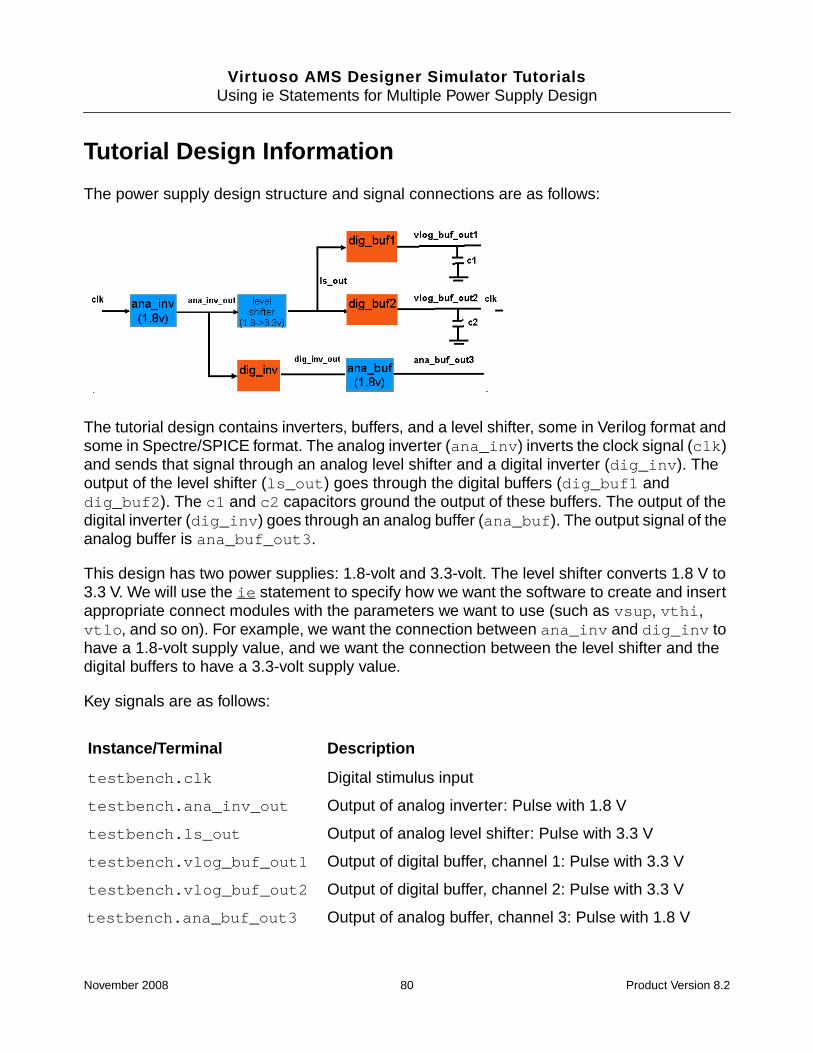
Virtuoso AMS Designer Simulator TutorialsUsing ie Statements for Multiple Power Supply Design
Tutorial Design Information
The power supply design structure and signal connections are as follows:
The tutorial design contains inverters, buffers, and a level shifter, some in Verilog format andsome in Spectre/SPICE format. The analog inverter (ana_inv) inverts the clock signal (clk)and sends that signal through an analog level shifter and a digital inverter (dig_inv). Theoutput of the level shifter (ls_out) goes through the digital buffers (dig_buf1 anddig_buf2). The c1 and c2 capacitors ground the output of these buffers. The output of thedigital inverter (dig_inv) goes through an analog buffer (ana_buf). The output signal of theanalog buffer is ana_buf_out3.
This design has two power supplies: 1.8-volt and 3.3-volt. The level shifter converts 1.8 V to3.3 V. We will use the ie statement to specify how we want the software to create and insertappropriate connect modules with the parameters we want to use (such as vsup, vthi,vtlo, and so on). For example, we want the connection between ana_inv and dig_inv tohave a 1.8-volt supply value, and we want the connection between the level shifter and thedigital buffers to have a 3.3-volt supply value.
Key signals are as follows:
Instance/Terminal Description
testbench.clk Digital stimulus input
testbench.ana_inv_out Output of analog inverter: Pulse with 1.8 V
testbench.ls_out Output of analog level shifter: Pulse with 3.3 V
testbench.vlog_buf_out1 Output of digital buffer, channel 1: Pulse with 3.3 V
testbench.vlog_buf_out2 Output of digital buffer, channel 2: Pulse with 3.3 V
testbench.ana_buf_out3 Output of analog buffer, channel 3: Pulse with 1.8 V
November 2008 80 Product Version 8.2
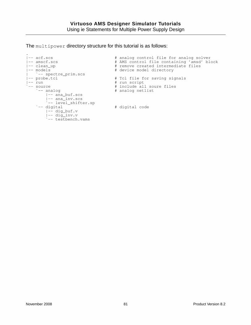
Virtuoso AMS Designer Simulator TutorialsUsing ie Statements for Multiple Power Supply Design
The multipower directory structure for this tutorial is as follows:
.|-- acf.scs # analog control file for analog solver|-- amscf.scs # AMS control file containing ’amsd’ block|-- clean_up # remove created intermediate files|-- models # device model directory| `-- spectre_prim.scs|-- probe.tcl # Tcl file for saving signals|-- run # run script`-- source # include all soure files
`-- analog # analog netlist|-- ana_buf.scs|-- ana_inv.scs`-- level_shifter.sp
`-- digital # digital code|-- dig_buf.v|-- dig_inv.v `-- testbench.vams
November 2008 81 Product Version 8.2
Virtuoso AMS Designer Simulator TutorialsUsing ie Statements for Multiple Power Supply Design
Running the Tutorial
To run this tutorial, do the following in the multpower directory:
1. Examine the ie statements in the amscf.scs file:
amsd {...ie vsup=1.8ie vsup=3.3 cell=dig_buf}
The first ie statement above defines 1.8 volts as the global default power supply setting.All connect modules that you do not otherwise customize use this value.Any customizations you specify apply to domainless nets only.
The second ie statement above defines a scope for the 3.3-volt power supply: at theboundaries of the digbuf cell.
2. Examine the run script:
We strongly recommend you use the -chkdigdisp command-line option when you areverifying designs that have more than one power supply. This option causes theelaborator to scan the design and identify any nets with incompatible digital disciplineconnections using proprietary rules. The elaborator reports any errors with completeinformation about the incompatible discipline and connection so that you can verifymultiple-supply connectivity without running laborious analog simulations.
3. Run the tutorial:
./run
The tutorial runs using the AMS Designer simulator with the UltraSim solver.
irun ./source/digital/*.v \ Verilog input files
./source/digital/*.vams \ Verilog-AMS input files
./amscf.scs \ AMS control file
-amsfastspice \ Enable UltraSim solver
-timescale 1ns/100ps \ Set digital timescale
-iereport \ Generate IE report
-input probe.tcl \ Tcl probe file
-chkdigdisp Check compatibility ofdiscrete (digital) disciplines
November 2008 82 Product Version 8.2
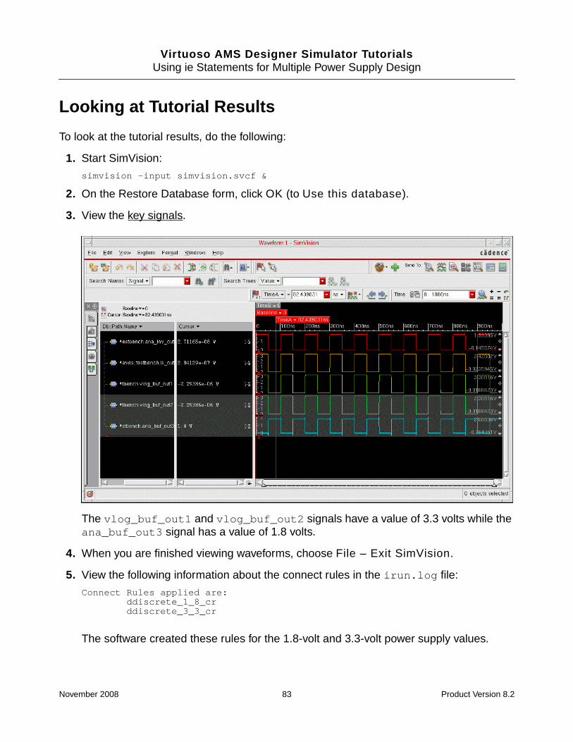
Virtuoso AMS Designer Simulator TutorialsUsing ie Statements for Multiple Power Supply Design
Looking at Tutorial Results
To look at the tutorial results, do the following:
1. Start SimVision:
simvision -input simvision.svcf &
2. On the Restore Database form, click OK (to Use this database).
3. View the key signals.
The vlog_buf_out1 and vlog_buf_out2 signals have a value of 3.3 volts while theana_buf_out3 signal has a value of 1.8 volts.
4. When you are finished viewing waveforms, choose File – Exit SimVision.
5. View the following information about the connect rules in the irun.log file:
Connect Rules applied are:ddiscrete_1_8_crddiscrete_3_3_cr
The software created these rules for the 1.8-volt and 3.3-volt power supply values.
November 2008 83 Product Version 8.2
Virtuoso AMS Designer Simulator TutorialsUsing ie Statements for Multiple Power Supply Design
6. View the IE Report Summary (also in the irun.log file) to see that the elaboratorinserted six connect modules:
IE Report SummaryBidir_2 ( logic inout; electrical inout; ) total: 1E2L_2 ( electrical input; logic inout; ) total: 2L2E_2 ( logic input; electrical inout; ) total: 3
----------------------------------------------------------------Total Number of Connect Modules total: 6
7. (Optional) Run the clean-up script to clean up generated files:
./clean_up
November 2008 84 Product Version 8.2
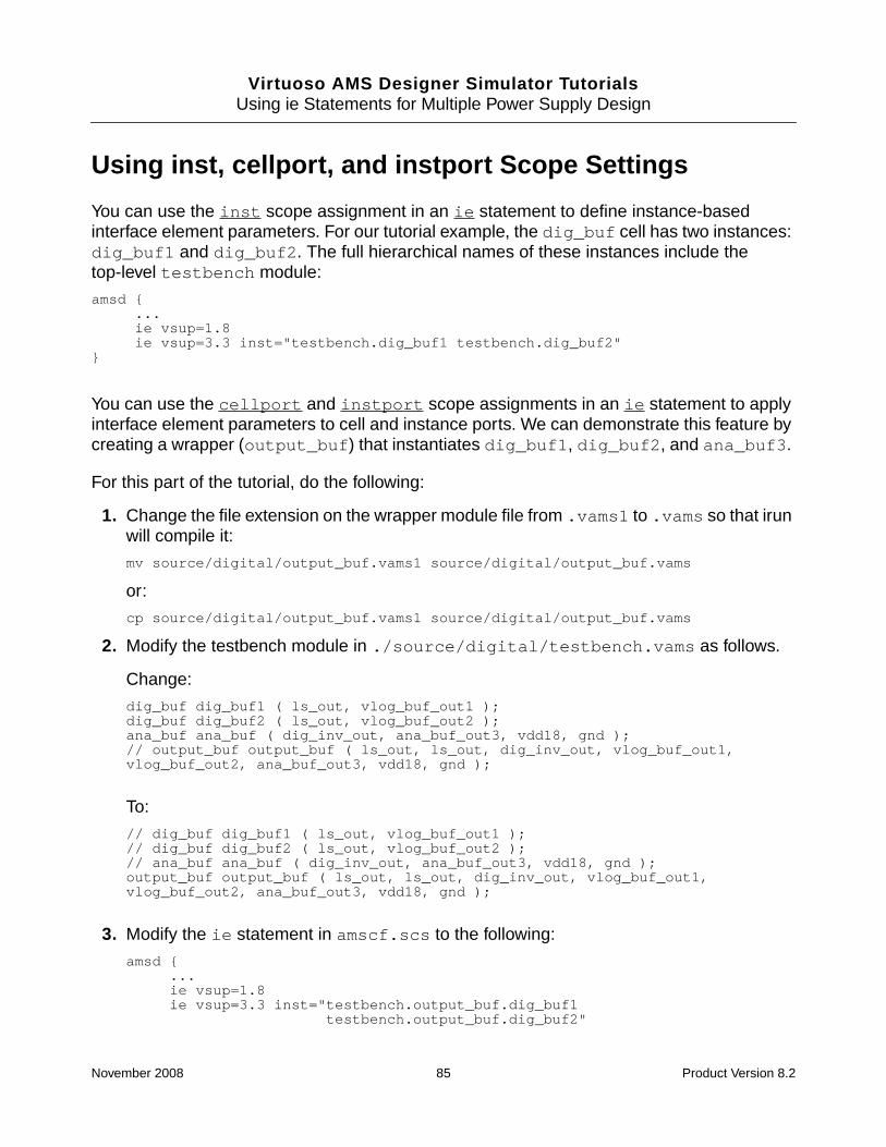
Virtuoso AMS Designer Simulator TutorialsUsing ie Statements for Multiple Power Supply Design
Using inst, cellport, and instport Scope Settings
You can use the inst scope assignment in an ie statement to define instance-basedinterface element parameters. For our tutorial example, the dig_buf cell has two instances:dig_buf1 and dig_buf2. The full hierarchical names of these instances include thetop-level testbench module:
amsd {...ie vsup=1.8ie vsup=3.3 inst="testbench.dig_buf1 testbench.dig_buf2"
}
You can use the cellport and instport scope assignments in an ie statement to applyinterface element parameters to cell and instance ports. We can demonstrate this feature bycreating a wrapper (output_buf) that instantiates dig_buf1, dig_buf2, and ana_buf3.
For this part of the tutorial, do the following:
1. Change the file extension on the wrapper module file from .vams1 to .vams so that irunwill compile it:
mv source/digital/output_buf.vams1 source/digital/output_buf.vams
or:
cp source/digital/output_buf.vams1 source/digital/output_buf.vams
2. Modify the testbench module in ./source/digital/testbench.vams as follows.
Change:
dig_buf dig_buf1 ( ls_out, vlog_buf_out1 );dig_buf dig_buf2 ( ls_out, vlog_buf_out2 );ana_buf ana_buf ( dig_inv_out, ana_buf_out3, vdd18, gnd );// output_buf output_buf ( ls_out, ls_out, dig_inv_out, vlog_buf_out1,vlog_buf_out2, ana_buf_out3, vdd18, gnd );
To:
// dig_buf dig_buf1 ( ls_out, vlog_buf_out1 );// dig_buf dig_buf2 ( ls_out, vlog_buf_out2 );// ana_buf ana_buf ( dig_inv_out, ana_buf_out3, vdd18, gnd );output_buf output_buf ( ls_out, ls_out, dig_inv_out, vlog_buf_out1,vlog_buf_out2, ana_buf_out3, vdd18, gnd );
3. Modify the ie statement in amscf.scs to the following:
amsd {...ie vsup=1.8ie vsup=3.3 inst="testbench.output_buf.dig_buf1
testbench.output_buf.dig_buf2"
November 2008 85 Product Version 8.2
Virtuoso AMS Designer Simulator TutorialsUsing ie Statements for Multiple Power Supply Design
}
tagit: verify above; should be cellport? instport?
4. Run the simulation:
./run
Messages such as the following appear:
ncelab: *E,DSPMM: Incompatible discrete disciplinestestbench.output_buf.in1(ddiscrete_1_8) connected totestbench.output_buf.dig_buf1.in(ddiscrete_3_3).
ncelab: *E,DSPMM: Incompatible discrete disciplinestestbench.output_buf.out1(ddiscrete_1_8) connected totestbench.output_buf.dig_buf1.out(ddiscrete_3_3).
ncelab: *E,DSPMM: Incompatible discrete disciplinestestbench.output_buf.in2(ddiscrete_1_8) connected totestbench.output_buf.dig_buf2.in(ddiscrete_3_3).
ncelab: *E,DSPMM: Incompatible discrete disciplinestestbench.output_buf.out2(ddiscrete_1_8) connected totestbench.output_buf.dig_buf2.out(ddiscrete_3_3).
irun: *E,ELBERR: Error during elaboration (status 1), exiting.
These errors, about incompatible digital disciplines, result from using the -chkdigdispcommand-line option.
The incompatibility results from dig_buf having a 3.3-volt discipline while the rest of thedigital domain has a 1.8-volt discipline.
5. Modify the ie statement in amscf.scs as follows to correct these errors by specifying3.3 volts for the cell ports:
amsd {...ie vsup=1.8ie vsup=3.3 cell=dig_bufie vsup=3.3 cellport="output_buf.in1 output_buf.in2
November 2008 86 Product Version 8.2
Virtuoso AMS Designer Simulator TutorialsUsing ie Statements for Multiple Power Supply Design
output_buf.out1 output_buf.out2"}
6. Run the simulation again:
./run
The simulation runs to completion.
To view the waveforms, do the following:
1. Start SimVision:
simvision -input simvision.svcf &
2. View these key values:
testbench.clktestbench.ana_inv_outtestbench.ls_outtestbench.vlog_buf_out1testbench.vlog_buf_out2testbench.ana_buf_out3
Again, vlog_buf_out1 and vlog_buf_out2 have a value of 3.3 volts whileana_buf_out3 has a value of 1.8 volts.
3. (Optional) Run the clean-up script to clean up generated files:
./clean_up
November 2008 87 Product Version 8.2

Virtuoso AMS Designer Simulator TutorialsUsing ie Statements for Multiple Power Supply Design
November 2008 88 Product Version 8.2
Virtuoso AMS Designer Simulator Tutorials
12Real Modeling with the AMS DesignerSimulator
AMS-Spectre means the Virtuoso® AMS Designer simulator using the Spectre solver.AMS-UltraSim means the Virtuoso AMS Designer simulator using the UltraSim solver.
Note: The estimated time to complete this tutorial is about 25 minutes.
Using either Verilog-AMS or VHDL-AMS languages, you can define real ports that are notelectrical. Using “real modeling” technology, the elaborator automatically inserts appropriateconnect modules between electrical ports (analog domain) and wreal ports (digital domain)so that you can benefit from increased simulation speed. In this tutorial, we introduce realmodeling technology using simple test cases that highlight the main capabilities andadvantages.
This tutorial illustrates the following:
■ Real modeling for a 14-bit ADC and a 14-bit DAC in Verilog-AMS
■ Real modeling for a 14-bit DAC in VHDL-AMS
■ R2E (real-to-electrical), E2R (electrical-to-real), and ER_bidir (bidirectionalelectrical-to-real) connect modules on simple circuits
You can use wreal connect modules to connect real modeling models to Spectre or SPICEor electrical blocks. Real connect modules offer analog/digital (discrete wreal) conversionwith a user-defined variable rate. wreal connect modules support variable rate signalconversion for better performance. The absdelta function drives the real connect moduleA-to-D conversion. Digital events drive the real connect module D-to-A conversion.
See the following topics for tutorial details:
■ Test Case Information on page 90
■ Running the Tutorial on page 91
November 2008 89 Product Version 8.2
Virtuoso AMS Designer Simulator TutorialsReal Modeling with the AMS Designer Simulator
Test Case Information
This tutorial covers two different topics:
■ Real modeling: The test bench, top, instantiates one step ramp source connected to theinput of a 14-bit ADC. The 14 output bits of this ADC connect to the inputs of a DAC. Wecreated a real DC source to define the supply and the LSB values of these twomixed-signal converters. We will exercise and simulate all possible conversions of theADC and DAC. Because there are 14 bits, the number of conversions to simulate is2**14=16384. The transistor-level simulation of the real IC for this number of conversionscan take from a few days to more than a week.
■ E2R, R2E, ER_bidir: We will examine these connect modules and learn how theelaborator inserts them automatically for Verilog-AMS using a small test bench.
The test case directory/file structure is as follows:
.|-- amscf.scs # AMS control file|-- clean_up # clean-up script|-- run1_adc_dac # run script for top_adc_dac.vams simulation|-- run1_adc_dac.tcl # Tcl script for top_adc_dac.vams simulation|-- run2_adc_dac_vhms # run script for top_adc_dac.vhms simulation|-- run2_adc_dac_vhms.tcl # Tcl script for top_adc_dac.vhms simulation|-- run3_top_R2E # run script for R2E_example.vams simulation|-- run3_top_R2E.tcl # Tcl script for R2E_example.vams simulation|-- run4_top_ER_bidir # run script for top_adc_dac_rload.vams simulation|-- run5_top_E2R # run script for top_E2R.vams simulation|-- source # sub-directory including all source files| |-- adc14.vams # real model of 14-bit ADC in Verilog-AMS| |-- clock_gen.vams # clock generator| |-- dac14.vams # real model for 14-bit DAC in Verilog-AMS| |-- dac14.vhms # real model for 14-bit DAC in VHDL-AMS| |-- R2E_example.vams # test bench for the R2E| |-- rdcsource.vams # real model for DC source| |-- step.vams # real model for step source| |-- step_bidir.vams # real model for step source, ER_bidir case| |-- top_adc_dac.vams # Verilog-AMS test bench for 14-bit ADC+DAC| |-- top_adc_dac.vhms # VHDL-AMS test bench for 14-bit ADC+DAC| |-- top_adc_dac_rload.vams # Verilog-AMS test bench for 14-bit ADC+DAC| |-- top_E2R.vams # test bench for the E2R study`-- tran.scs # analog control file containing tran setup
November 2008 90 Product Version 8.2
Virtuoso AMS Designer Simulator TutorialsReal Modeling with the AMS Designer Simulator
Running the Tutorial
Important
Before starting this tutorial, see “Before You Begin” on page 9.
Running the tutorial consists of the following segments, in order:
■ wreal Modeling in Verilog-AMS on page 91
■ wreal Modeling in VHDL-AMS on page 93
■ R2E Connect Module on page 94
■ ER_bidir Connect Module on page 97
■ E2R Connect Module on page 99
➤ Change to the tutorial directory. For example:
cd real_modeling
wreal Modeling in Verilog-AMS
For this segment of the tutorial, do the following:
1. Examine the following files:
❑ source/rdcsource.vams contains the real type model for a DC source. Theoutput port type is wreal, which is like a wire with the capability to transfer a realnumber.
❑ source/step.vams contains the real type model for a ramp source. An externalclock defines the sampling rate.
❑ source/adc14.vams contains an example of a real type model for an ideal 14-bitADC.
❑ source/dac14.vams contains an example of a real type model for an ideal 14-bitDAC.
Note: The Verilog-AMS code for the ideal ADC and DAC is fairly efficient so that thesimulation runs quickly.
2. Examine the irun command in the run1_adc_dac run script.
The options -ACCESS +r (or +rwc) let you use the SimVision debugger to display objectvalues and see the connectivity.
November 2008 91 Product Version 8.2
Virtuoso AMS Designer Simulator TutorialsReal Modeling with the AMS Designer Simulator
3. Run the simulation:
./run1_adc_dac
Several key signals appear in the SimVision Waveform window.
4. On the Design Browser tab in the Design Brower window, right-click top in thesimulator tree and select Send to Schematic Tracer.
5. In the Schematic Tracer window, double-click the simulator::top rectangle.
The block diagram for the design appears.
6. In the SimVision Waveform window, click the run button.
The simulation completes in less than 3 seconds for 2**14=16384 ACD and DAC bitconversions. In this test case, the clock frequency is 1GHz. The ADC and DAC performa conversion on each positive edge of the clock. All signals are discrete in this dataflowsimulation.
7. In the SimVision Waveform window, select the signals rin and aout.
Tip
Click simulator::top.rin, then hold down the Ctrl key while clickingsimulator::top.aout.
8. To change the format of these signals, choose Format – Trace – Digital.
Observe the delay of two clock periods between the input source rin signal and theoutput after the ADC + DAC conversion, signal aout.
9. Choose File – Exit SimVision.
November 2008 92 Product Version 8.2
Virtuoso AMS Designer Simulator TutorialsReal Modeling with the AMS Designer Simulator
wreal Modeling in VHDL-AMS
We wrote the 14-bit DAC model in VHDL-AMS in this test case using discrete real ports forthe analog signals. We defined the LSB default value in a package. To perform the wrealmodeling exercise for this segment of the tutorial, do the following:
Note: You can exectue the same steps as in “wreal Modeling in Verilog-AMS” on page 91.Notice that the name of the run script is different.
1. Examine source/source/dac14.vhms and source/top_adc_dac.vhms.
In this example, we instantiate both VHDL-AMS entities and Verilog-AMS modules.
2. Run the simulation:
./run2_adc_dac_vhms
Several key signals appear in the SimVision Waveform window.
3. On the Design Browser tab in the Design Brower window, right-clickWORKLIB:TOP(BHV) in the simulator tree and select Send to Schematic Tracer.
4. In the Schematic Tracer window, double-click the WORKLIB:TOP(BHV) rectangle.
The block diagram for the design appears.
5. In the SimVision Waveform window, click the run button.
The simulation completes in less than 3 seconds for 2**14=16384 ACD and DAC bitconversions. In this test case, the clock frequency is 1GHz. The ADC and DAC performa conversion on each positive edge of the clock. All signals are discrete in this dataflowsimulation.
6. In the SimVision Waveform window, select the signals rin and aout.
Tip
Click simulator::top.rin, then hold down the Ctrl key while clickingsimulator::top.aout.
7. To change the format of these signals, choose Format – Trace – Digital.
Observe the delay of two clock periods between the input source rin signal and theoutput after the ADC + DAC conversion, signal aout.
8. Choose File – Exit SimVision.
November 2008 93 Product Version 8.2
Virtuoso AMS Designer Simulator TutorialsReal Modeling with the AMS Designer Simulator
R2E Connect Module
For this segment of the tutorial, we will examine the insertion of the R2E (real-to-electrical)connect module. We will also observe the custom connect rule the software generatesautomatically as a result of the ie statement in the amsd block.
Note: See also “E2R Connect Module” on page 99.
To examine the insertion of the R2E (real-to-electrical) connect module, do the following:
1. Examine source/step.vams.
The output of this generator is a wreal type. We used real modeling to design this ramp.The discipline is logic.
2. Examine the source/R2E_example.vams test bench file.
Signal aout is an electrical net. The step generator drives the electrical primitiveresistor. During elaboration, the software inserts an R2E connect module.
The RLOAD2 resistance value is 200 Ohms. We chose this value to create a divider bytwo (because the R2E output impedance is 200 Ohms).
3. Run the simulation:
./run3_top_R2E
Because we added the -IEREPORT option to the irun command, we get the followingreport about interface element insertion at the end of elaboration:
----------IE report -------------
Automatically inserted instance: top.aout__R2E__logic (merged):connectmodule name: R2E,inserted across signal: aoutand ports of discipline: logicSensitivity infomation:
No Sensitivity infoDiscipline of Port (Din): logic, Digital portDrivers of port Din:
(top.I2) assign y = yvalLoads of port Din:
Load: VST_S_BLOCKING_ASSIGNMENT, Line 49, Index 0,in: top.aout__R2E__logic
Discipline of Port (Aout): electrical, Analog port----------end IE report -------------
4. Examine the following command in the run3_top_R2E.tcl Tcl script, which we use toget the domain descriptions of the signals:
describe -verbose top.*top.gnd....analog net (electrical) = 0top.aout...analog net (electrical) = 0top.clk....net (wire/tri) logic = St0
November 2008 94 Product Version 8.2
Virtuoso AMS Designer Simulator TutorialsReal Modeling with the AMS Designer Simulator
The software inserts one R2E connect module on net top.aout.
5. In the SimVision Waveform window, click the run button.
The simulation completes. You can do a zoom fit to see five events on the aout signal.
At the end of the simulation, the simulator reports the activity in the SimVision console:
**** AMSD: Mixed-Signal Activity Statistics ****Number of A-to-D events: 0Number of A-to-D events in IEs: 0Number of D-to-A events: 5Number of D-to-A events in IEs: 5Number of VHDL-AMS Breaks: 0
The number of D-to-A events in interface elements is 5, which matches the number ofstep executions for the aout signal. The R2E introduces multirate sampling.
6. In the SimVision Waveform window, select signal yval.
7. To change the format of this signal, choose Format – Trace – Digital.
Observe the high activity. The clock period of 1 ns forces the step block to generate anew sample value every 1 ns. The R2E operates like a sample-and-hold.vdelta=1.8V/64=0.028125 defines the step for the V(aout) signal. In the waveformdisplay, we see a step of 1.8/(64*2)= 0.0140625 Volts because the R2E outputimpedance is 200 Ohms and we have a resistor load of 200 Ohms.
8. Choose File – Exit SimVision.
November 2008 95 Product Version 8.2
Virtuoso AMS Designer Simulator TutorialsReal Modeling with the AMS Designer Simulator
To observe the custom connect rules the software generates automatically as a result of theie statement in the amsd block, do the following:
1. Examine the ie statement in the amsd block in the AMS control file, amscf.scs:
include "tran.scs"amsd {
ie vsup=1.8}
The software creates a set of 1.8 Volt “full-fast” connect rules based on this statement.
2. After the simulation runs, examine the amscb_ie_crules.vams connect rules file thatthe software automatically creates in the hidden directory, .ams_spice_in:
...// using connectrule: full_fastdiscipline discrete_18__1domain discrete;
enddiscipline
`define Vsup1 1.8`define Vthi1 1.20`define Vtlo1 0.60`define Tr1 0.2n`define Rlo1 200.0`define Rhi1 200.0`define Rx1 40.0`define Rz1 10.0M`define Vdelta1 `Vsup1/64.0`define Vdelta_tol1 `Vdelta1/4.0`define Tr_delta1 `Tr1/20.0connectrules discrete_18__1_cr;connect L2E_2 #(
.vsup(`Vsup1),
.tr(`Tr1), .tf(`Tr1),
.rlo(`Rlo1), .rhi(`Rhi1), .rx(`Rx1), .rz(`Rz1) ) discrete_18__1,electrical;connect E2L_2 #(
.vsup(`Vsup1), .vthi(`Vthi1), .vtlo(`Vtlo1), .tr(`Tr1) ) electrical,discrete_18__1;connect Bidir_2 #(
.vsup(`Vsup1), .vthi(`Vthi1), .vtlo(`Vtlo1),
.tr(`Tr1), .tf(`Tr1),
.rlo(`Rlo1), .rhi(`Rhi1), .rx(`Rx1), .rz(`Rz1) ) discrete_18__1,electrical;connect E2R #(.vdelta(`Vdelta1), .vtol(`Vdelta_tol1), .ttol(`Tr_delta1))electrical, discrete_18__1;connect R2E #(.vdelta(`Vdelta1), .tr(`Tr_delta1), .tf(`Tr_delta1),.rout(`Rlo1)) discrete_18__1, electrical;connect ER_bidir #(.vdelta(`Vdelta1), .vtol(`Vdelta_tol1), .ttol(`Tr_delta1),
.tr(`Tr_delta1), .tf(`Tr_delta1), .rout(`Rlo1), .rz(`Rz1))discrete_18__1, electrical;endconnectrules
November 2008 96 Product Version 8.2
Virtuoso AMS Designer Simulator TutorialsReal Modeling with the AMS Designer Simulator
ER_bidir Connect Module
For this segment of the tutorial, we will examine the insertion of the ER_bidir (electrical-to-realbidirectional) connect module. Using the same test case, we changed the wreal output portfrom output y to inout y. To view these differences, you can use the UNIX sdiffcommand as follows:
sdiff -s source/step.vams source/step_bidir.vams
output y; | inout y;
To perform this segment of the tutorial, do the following:
1. Run the simulation:
./run4_top_ER_bidir
2. Examine the same run3_top_R2E.tcl Tcl script we used for “R2E Connect Module”on page 94 which contains the command we use to get the domain descriptions of thesignals:
describe -verbose top.*top.gnd....analog net (electrical) = 0top.aout...wire (real) = 0top.clk....net (wire/tri) logic = St0
The software inserts one bidirectional connect module on wreal net top.aout.
3. In the SimVision Waveform window, click the run button.
The simulation completes. You can do a zoom fit to see five events on the aout signal.
At the end of the simulation, the simulator reports the activity in the SimVision console:
**** AMSD: Mixed-Signal Activity Statistics ****Number of A-to-D events: 6Number of A-to-D events in IEs: 6Number of D-to-A events: 6Number of D-to-A events in IEs: 6Number of VHDL-AMS Breaks: 0
The number of D-to-A events in interface elements is 6.
At time =0, the function absdelta(V(Aout), vdelta, ttol, vtol)) triggers anadditional event in the simulator. With the absdelta function, at time 0, the signalconversion happens unconditionally.
4. In the SimVision Waveform window, select signal yval.
5. To change the format of this signal, choose Format – Trace – Digital.
November 2008 97 Product Version 8.2

Virtuoso AMS Designer Simulator TutorialsReal Modeling with the AMS Designer Simulator
Observe the high activity. The clock period of 1 ns forces the step block to generate anew sample value every 1 ns. The ER_bidir operates like a sample-and-hold.
6. Choose File – Exit SimVision.
November 2008 98 Product Version 8.2
Virtuoso AMS Designer Simulator TutorialsReal Modeling with the AMS Designer Simulator
E2R Connect Module
For this segment of the tutorial, we will examine the insertion of the E2R (electrical-to-real)connect module. The sample test bench circuit is a SPICE voltage PWL source that drives awreal gain amplifier. The vsource PWL definition is as follows:
wave({0,0,10u,0.1})
Note: See also “R2E Connect Module” on page 94.
1. Examine source/top_E2R.vams.
On electrical node v_in, we connect the PWL SPICE source to the real modelingamplifier. The real amplifier is a synchronous real modeling style example. The code isas follows:
module rgain (din, dout );input din;output dout;wreal din, dout;parameter real gain=1.0;assign dout = gain * din;
endmodule
Every time the real discrete input signal (din) changes, the output signal (dout)changes.
2. Run the simulation:
./run5_top_E2R
3. Examine the same run3_top_R2E.tcl Tcl script we used for “R2E Connect Module”on page 94 which contains the command we use to get the domain descriptions of thesignals:
describe -verbose top.*top.gnd.....analog net (electrical) = 0top.v_in....analog net (electrical) = 2e-07top.v_out...wire(real)
4. In the SimVision Console window, type the following command to display the IE report.
scope -aicms -all
The following report appears:
Instance: top.v_in__E2R__discrete_18__1 (merged) is:instance of connect_module: E2R__discrete_18,inserted across signal: top.v_in,and ports of discipline: 1.
The software inserted one E2R connect module.
November 2008 99 Product Version 8.2
Virtuoso AMS Designer Simulator TutorialsReal Modeling with the AMS Designer Simulator
5. In the SimVision Waveform window, click the run button.
At the end of the simulation, the simulator reports the activity in the SimVision console:
**** AMSD: Mixed-Signal Activity Statistics ****Number of A-to-D events: 6Number of A-to-D events in IEs: 6Number of D-to-A events: 0Number of D-to-A events in IEs: 0Number of VHDL-AMS Breaks: 0
The number of A-to-D events is the same as the number of A-to-D events in interfaceelements in this example. This is not always the case, for example, if you use in analways condition a cross function on an analog signal.
6. Zoom fit and select signals v_in and v_out.
Tip
Select v_in, then hold down the Ctrl key while selecting v_out.
7. To change the format of these signals, choose Format – Trace – Digital.
Observe the lower activity between 0 and 10 µs on v_out: The v_out discrete signalchanges six times. This behavior comes from the E2R connect module whose code is asfollows:
connectmodule E2R (Ain, Dout);input Ain;electrical Ain; //input electricaloutput Dout;wreal Dout; //output wreal\logic Dout; //discrete domain
parameter real vdelta=1.8/64 from (0:inf); // voltage deltaparameter real vtol=vdelta/4 from (0:vdelta); // voltage toleranceparameter real ttol=10p from (0:1m]; // time tolerance
real Dreg; //real register for A to D wreal conversion
assign Dout = Dreg;
//discretize V(Ain) triggered by absdelta functionalways @(absdelta(V(Ain), vdelta, ttol, vtol))
Dreg = V(Ain);endmodule
Note: You can find this code in your_install_dir/tools/affirma_ams/etc/connect_lib/E2R.vams.
November 2008 100 Product Version 8.2
Virtuoso AMS Designer Simulator TutorialsReal Modeling with the AMS Designer Simulator
The absdelta function drives the electrical-to-real conversion. Using absdelta, wecan generate events whenever the signal changes more than a delta (defined byvdelta) from the previous conversion signal value, and a new conversion occurs. Theabsdelta function takes a time tolerance argument (ttol), which gets its value fromthe following value in .ams_spice_in/amscb_ie_crules.vams:
`define Tr_delta1 `Tr1/20.0
The vdelta value is 2.000000e-02 Volts. The always @(absdelta(V(Ain),vdelta, ttol, vtol)) statement triggers the probing of the input port of the E2Rconnect module. This sampling magnitude comes from the following parameters in theconnect rule:
vdelta=Vsup/64=0.028125
vtol=vdelta/4=7.031E-03
8. Choose File – Exit SimVision.
Cadence provides a set of fixed-voltage connect rules for 1.8V, 3V, and 5V (ConnRules18,ConnRules3, and ConnRules5) with wreal connect modules in the installation hierarchy.You can use the connect modules that Cadence provides and customize them according toyour connection requirements using ie statements in an amsd block.
November 2008 101 Product Version 8.2

Virtuoso AMS Designer Simulator TutorialsReal Modeling with the AMS Designer Simulator
November 2008 102 Product Version 8.2
Virtuoso AMS Designer Simulator Tutorials
13Using AMS Designer with SystemVerilog
SystemVerilog is a hardware design and verification language that has the followingverification-focused features:
■ Dynamic data types, such as classes and various kinds of arrays
■ Constrained randomization for stimulus generation
■ Functional coverage
■ Property definition and assertions
■ Advanced use of interfaces for transaction-based verification (TBV)
■ Interprocess synchronization
■ Programming constructs, such as clocking blocks, final blocks, and programs
■ Direct programming interface (DPI)
You can use SystemVerilog (as well as other digital languages, such as Specman e andSystemC) with AMS Designer to blend digital regression and validation methodology intoanalog/mixed-signal. (Note that digital-centric validation tools such as Specman now supportanalog/mixed-signal capabilities such as real-number read/write so that you can performsuch tasks as coverage, constraint, regression, and so on.)
High-speed SerDes (serializer/deserializer) and RF designs are mixed-signal by nature, andhave complex interactions between the analog circuitry and the digital control blocks. Theselarger and more complex designs require more accurate analog simulation, even at a veryhigh level of abstraction. It is no longer enough to perform block-level SPICE simulation andfull-chip simulation using simple digital HDL models to represent analog blocks. Instead, youcan use the AMS Designer simulator for fast and accurate full-chip simulation.
See the following topics for tutorial information:
■ Test Case Information on page 104
■ Running the Tutorial on page 106
November 2008 103 Product Version 8.2
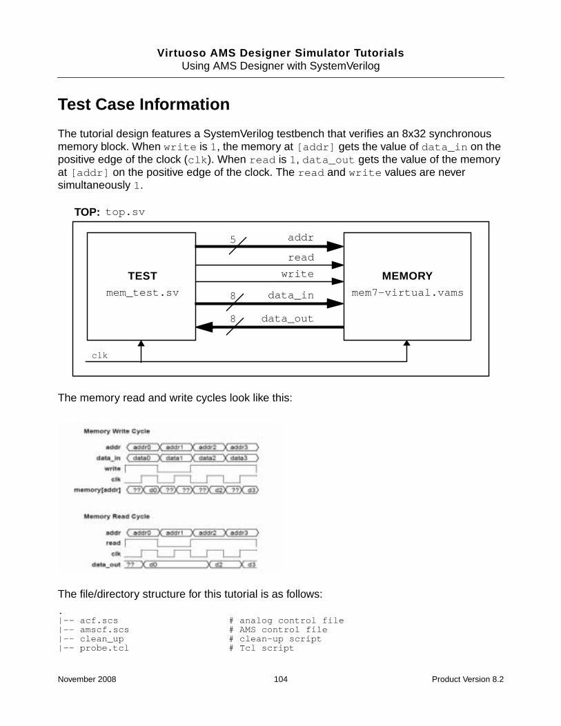
Virtuoso AMS Designer Simulator TutorialsUsing AMS Designer with SystemVerilog
Test Case Information
The tutorial design features a SystemVerilog testbench that verifies an 8x32 synchronousmemory block. When write is 1, the memory at [addr] gets the value of data_in on thepositive edge of the clock (clk). When read is 1, data_out gets the value of the memoryat [addr] on the positive edge of the clock. The read and write values are neversimultaneously 1.
The memory read and write cycles look like this:
The file/directory structure for this tutorial is as follows:
.|-- acf.scs # analog control file|-- amscf.scs # AMS control file|-- clean_up # clean-up script|-- probe.tcl # Tcl script
TESTmem_test.sv
MEMORYmem7-virtual.vams
addr
read
write
data_in
data_out
5
8
8
clk
TOP: top.sv
November 2008 104 Product Version 8.2

Virtuoso AMS Designer Simulator TutorialsUsing AMS Designer with SystemVerilog
|-- run # run script'-- source # source files
|-- mem7-virtual.vams # Verilog-AMS memory block, module mem|-- mem_test.sv # SystemVerilog testbench, module mem_test'-- top.sv # SystemVerilog top-level wrapper containing
instances of both mem and mem_test
November 2008 105 Product Version 8.2
Virtuoso AMS Designer Simulator TutorialsUsing AMS Designer with SystemVerilog
Running the Tutorial
Important
Before starting this tutorial, see “Before You Begin” on page 9.
To run this tutorial, do the following:
1. Change to the tutorial directory:
cd sv_ams
2. Examine the Verilog-AMS memory module in mem7-virtual.vams.
3. Examine the SystemVerilog testbench module in mem_test.sv to observe the followingverification features of the language:
❑ write_mem and read_mem tasks:
task write_mem ( input [4:0] waddr, input [7:0] wdata, input debug=0 ) ;...endtask
...task read_mem ( input [4:0] raddr, output [7:0] rdata, input debug = 0 ) ;...endtask
❑ class memrand, which generates directed-random stimulus:
class memrand;...endclass
❑ Functional coverage:
covergroup coverrand @(posedge clk iff (collect_coverage && write));cp_addr: coverpoint addr;cp_data_in: coverpoint data_in {bins uppercase = {[8'h41:8'h5a]};bins lowercase = {[8'h61:8'h7a]};bins wantempty = default;
}endgroup : coverrandcoverrand coverrand_i = new;
4. Examine the top-level SystemVerilog wrapper module in top.sv, which containsinstances of mem (from mem7-virtual.vams) and mem_test (from mem_test.sv).
5. Examine the irun command in the run script:
irun source/*.sv \ SystemVerilog input files
November 2008 106 Product Version 8.2
Virtuoso AMS Designer Simulator TutorialsUsing AMS Designer with SystemVerilog
6. Use the script to run irun:
./run
7. Start SimVision:
simvision &
8. Choose File – Open Database to open the wave.trn file in the waves.shm directory.
9. Browse the signals, paying particular attention to the interface (connect) elements thesoftware inserted.
10. When you are finished viewing waveforms, choose File – Exit SimVision.
For additional tutorial information, see the following topics:
■ Viewing Coverage Results and Analyzing Coverage Data on page 108
■ Running the Tutorial Using the UltraSim Solver on page 110
source/*.vams \ Verilog-AMS input files
amscf.scs \ AMS control file
-coverage all -covoverwrite \ Enable coverage instrumentation
-input probe.tcl \ Tcl probe file
-timescale 1ns/100ps \ Set digital timescale
-iereport $1\ Generate IE report
-mess Generate messags
November 2008 107 Product Version 8.2
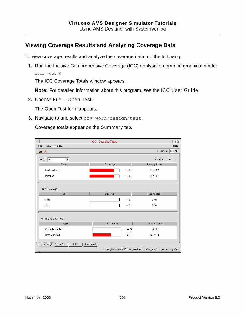
Virtuoso AMS Designer Simulator TutorialsUsing AMS Designer with SystemVerilog
Viewing Coverage Results and Analyzing Coverage Data
To view coverage results and analyze the coverage data, do the following:
1. Run the Incisive Comprehensive Coverage (ICC) analysis program in graphical mode:
iccr -gui &
The ICC Coverage Totals window appears.
Note: For detailed information about this program, see the ICC User Guide.
2. Choose File – Open Test.
The Open Test form appears.
3. Navigate to and select cov_work/design/test.
Coverage totals appear on the Summary tab.
November 2008 108 Product Version 8.2
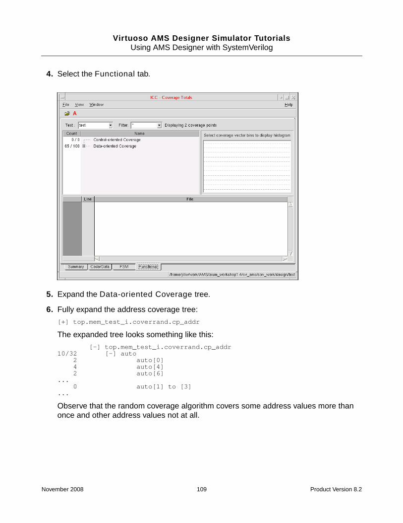
Virtuoso AMS Designer Simulator TutorialsUsing AMS Designer with SystemVerilog
4. Select the Functional tab.
5. Expand the Data-oriented Coverage tree.
6. Fully expand the address coverage tree:
[+] top.mem_test_i.coverrand.cp_addr
The expanded tree looks something like this:
[-] top.mem_test_i.coverrand.cp_addr10/32 [-] auto
2 auto[0]4 auto[4]2 auto[6]
...0 auto[1] to [3]
...
Observe that the random coverage algorithm covers some address values more thanonce and other address values not at all.
November 2008 109 Product Version 8.2
Virtuoso AMS Designer Simulator TutorialsUsing AMS Designer with SystemVerilog
7. Expand the input data coverage tree:
[+] top.mem_test_i.coverrand.cp_data_in
The expanded tree looks something like this:
[-] top.mem_test_i.coverrand.cp_data_in19 uppercase4 lowercase
The longer you run the test, the more closely the bins reflect your weighting.
o Expand your data coverpoint. You should see no coverage of the default values andmuch more coverage of lowercase values than uppercase values.
Running the Tutorial Using the UltraSim Solver
To run this tutorial example using the AMS Designer simulator with the UltraSim solver, dothe following:
➤ Add the -amsf command-line option as an argument to the run script:
./run -amsf
The -amsf command-line option selects and enables the UltraSim solver.
November 2008 110 Product Version 8.2
Virtuoso AMS Designer Simulator Tutorials
14Using Netlist Compiled Functions
When you run the Virtuoso® AMS Designer simulator with either analog solver (Spectre orUltraSim), you can have netlist expressions that call functions that the software loads from adynamic link library (DLL). You can create your own functions using C or C++ to takeadvantage of the features of these languages while overcoming restrictions on netlistuser-defined functions.
For more information about NCFs, see “Netlist Compiled Functions (NCFs)” in the VirtuosoSpectre Circuit Simulator User Guide.
To load the plug-in for netlist compiled functions (NCFs), use the -spectre_args or-ultrasim_args command-line option to pass the -plugin command-line option toSpectre or UltraSim. For example:
irun -spectre_args "-plugin libmyplugin_sh.so"
irun -amsfastspice -ultrasim_args "-plugin libmyplugin_sh.so"
Alternatively, you can use the loadplugin command in your Spectre netlist file.For example:
loadplugin "libmyplugin_sh.so"
Important
Before starting this tutorial, see “Before You Begin” on page 9.
See the following topics for tutorial details:
■ Tutorial Design Information on page 112
■ Running the Tutorial on page 115
November 2008 111 Product Version 8.2
Virtuoso AMS Designer Simulator TutorialsUsing Netlist Compiled Functions
Tutorial Design Information
This tutorial design is a PLL circuit that has a top-level Verilog testbench containing five majorblocks:
Verilog (testbench on top)||SPICE (PLL)||-----------------------|--------------------|--------------------|Verilog-A (VCO) SPICE (PD & CP) Verilog (divider) Verilog (counter)
The top-level testbench is a Verilog module that instantiates a SPICE block, pll_top. Insidepll_top, the VCO outputs eight evenly-spaced 400 MHz clocks, 45-degree phase apartfrom each other. One output clock (vcoclk) then passes through a divider and feeds backinto the phase detector (PD). The phase detector compares the incoming clock signal with theVCO output clock and produces either an up or a down signal to control the charging ordischarging of the charge pump (CP). As a result, the phase detector either raises or lowersthe VCO output clock frequency to bring it back in sync with the incoming clock. When thefeedback loop becomes stable, the VCO frequency locks to the frequency of the incomingsignal.
The ams_ncf directory and file structure for the tutorial files is as follows:
./|-- clean_up # clean-up script|-- models # model directory|-- probe.tcl # Tcl script for saving signals|-- amscf.scs # ‘amsd’ block and analog circuits included|-- run # run script with irun/amss control file|-- run_amsu # run script with irun/amsu control file|-- source # source file directory| |-- analog # analog netlist| | |-- ChargePump.sp # Charge Pump in SPICE| | |-- Gates.sp # Buffer in SPICE| | |-- PLL.sp # PLL in SPICE| | |-- PhaseDetector.sp # Phase Detector in SPICE| | `-- VCO.va # VCO in Verilog-A
Tutorial Design Block Language
Voltage-controlled oscillator (VCO) Verilog-A
Phase detector (PD) SPICE
Charge pump (CP) SPICE
Divider Verilog
Counter Verilog
November 2008 112 Product Version 8.2
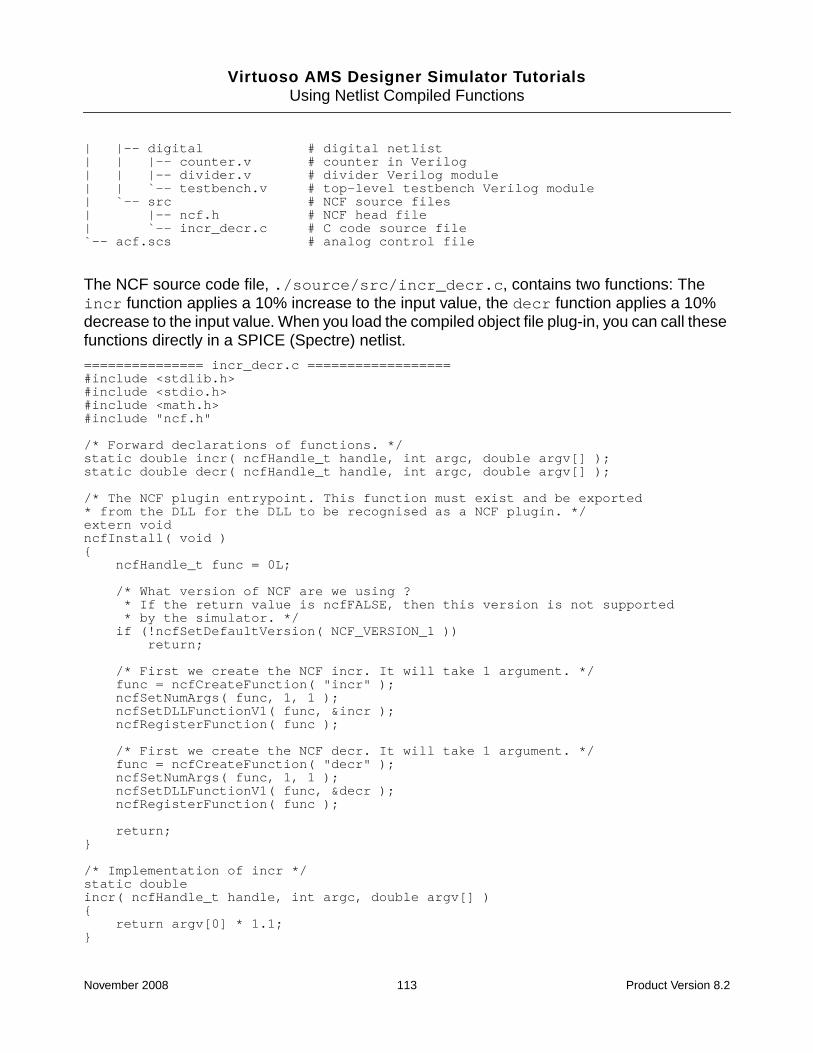
Virtuoso AMS Designer Simulator TutorialsUsing Netlist Compiled Functions
| |-- digital # digital netlist| | |-- counter.v # counter in Verilog| | |-- divider.v # divider Verilog module| | `-- testbench.v # top-level testbench Verilog module| `-- src # NCF source files| |-- ncf.h # NCF head file| `-- incr_decr.c # C code source file`-- acf.scs # analog control file
The NCF source code file, ./source/src/incr_decr.c, contains two functions: Theincr function applies a 10% increase to the input value, the decr function applies a 10%decrease to the input value. When you load the compiled object file plug-in, you can call thesefunctions directly in a SPICE (Spectre) netlist.
=============== incr_decr.c ==================#include <stdlib.h>#include <stdio.h>#include <math.h>#include "ncf.h"
/* Forward declarations of functions. */static double incr( ncfHandle_t handle, int argc, double argv[] );static double decr( ncfHandle_t handle, int argc, double argv[] );
/* The NCF plugin entrypoint. This function must exist and be exported* from the DLL for the DLL to be recognised as a NCF plugin. */extern voidncfInstall( void ){
ncfHandle_t func = 0L;
/* What version of NCF are we using ? * If the return value is ncfFALSE, then this version is not supported * by the simulator. */if (!ncfSetDefaultVersion( NCF_VERSION_1 ))
return;
/* First we create the NCF incr. It will take 1 argument. */func = ncfCreateFunction( "incr" );ncfSetNumArgs( func, 1, 1 );ncfSetDLLFunctionV1( func, &incr );ncfRegisterFunction( func );
/* First we create the NCF decr. It will take 1 argument. */func = ncfCreateFunction( "decr" );ncfSetNumArgs( func, 1, 1 );ncfSetDLLFunctionV1( func, &decr );ncfRegisterFunction( func );
return;}
/* Implementation of incr */static doubleincr( ncfHandle_t handle, int argc, double argv[] ){
return argv[0] * 1.1;}
November 2008 113 Product Version 8.2
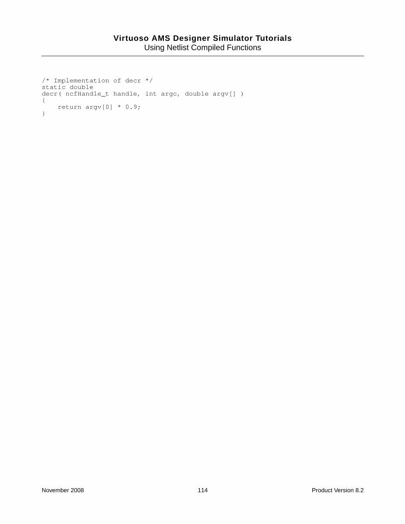
Virtuoso AMS Designer Simulator TutorialsUsing Netlist Compiled Functions
/* Implementation of decr */static doubledecr( ncfHandle_t handle, int argc, double argv[] ){
return argv[0] * 0.9;}
November 2008 114 Product Version 8.2
Virtuoso AMS Designer Simulator TutorialsUsing Netlist Compiled Functions
Running the Tutorial
To run the tutorial, do the following in the ams_ncf directory:
1. (Optional) Create the Compiled Shared Object File on page 116
2. Use the loadplugin Command in the Netlist on page 116
3. Use the -plugin Option on page 118
November 2008 115 Product Version 8.2
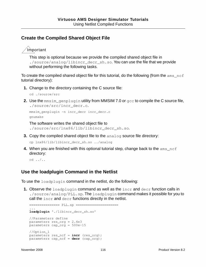
Virtuoso AMS Designer Simulator TutorialsUsing Netlist Compiled Functions
Create the Compiled Shared Object File
Important
This step is optional because we provide the compiled shared object file in./source/analog/libincr_decr_sh.so. You can use the file that we providewithout performing the following tasks.
To create the compiled shared object file for this tutorial, do the following (from the ams_ncftutorial directory):
1. Change to the directory containing the C source file:
cd ./source/src
2. Use the mmsim_genplugin utility from MMSIM 7.0 or gcc to compile the C source file,./source/src/incr_decr.c.
mmsim_genplugin -n incr_decr incr_decr.c
gnumake
The software writes the shared object file to./source/src/lnx86/lib/libincr_decr_sh.so.
3. Copy the compiled shared object file to the analog source file directory:
cp lnx86/lib/libincr_decr_sh.so ../analog
4. When you are finished with this optional tutorial step, change back to the ams_ncfdirectory:
cd ../..
Use the loadplugin Command in the Netlist
To use the loadplugin command in the netlist, do the following:
1. Observe the loadplugin command as well as the incr and decr function calls in./source/analog/PLL.sp. The loadplugin command makes it possible for you tocall the incr and decr functions directly in the netlist.
=============== PLL.sp =====================...loadplugin "./libincr_decr_sh.so"
//Parameters defineparameters res_org = 2.4e3parameters cap_org = 500e-15
//Option_1parameters res_ncf = incr (res_org);parameters cap_ncf = decr (cap_org);
November 2008 116 Product Version 8.2
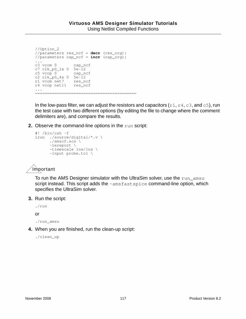
Virtuoso AMS Designer Simulator TutorialsUsing Netlist Compiled Functions
//Option_2//parameters res_ncf = decr (res_org);//parameters cap_ncf = incr (cap_org);...c3 vcom 0 cap_ncfc7 clk_p0_1x 0 5e-12c5 vcop 0 cap_ncfc2 clk_p0_4x 0 5e-12r1 vcom net7 res_ncfr4 vcop net11 res_ncf...==========================================
In the low-pass filter, we can adjust the resistors and capacitors (r1, r4, c3, and c5), runthe test case with two different options (by editing the file to change where the commentdelimiters are), and compare the results.
2. Observe the command-line options in the run script:
#! /bin/csh -firun ./source/digital/*.v \
./amscf.scs \-iereport \-timescale 1ns/1ns \-input probe.tcl \
Important
To run the AMS Designer simulator with the UltraSim solver, use the run_amsuscript instead. This script adds the -amsfastspice command-line option, whichspecifies the UltraSim solver.
3. Run the script:
./run
or
./run_amsu
4. When you are finished, run the clean-up script:
./clean_up
November 2008 117 Product Version 8.2
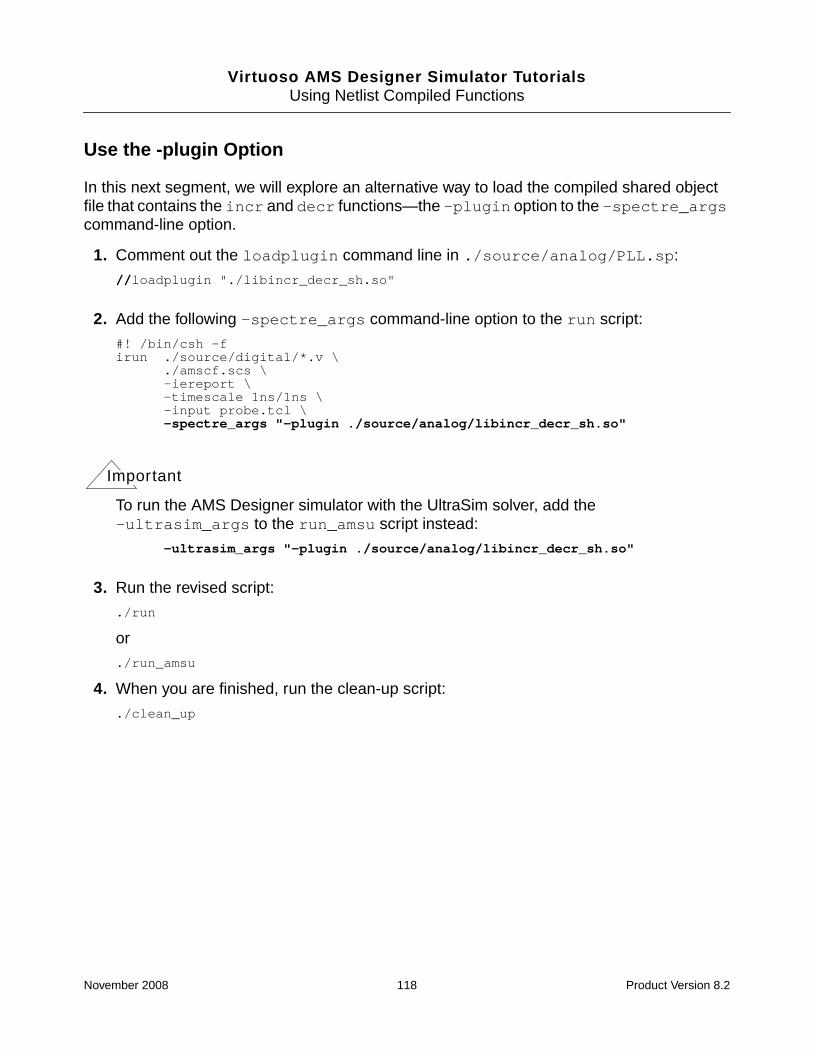
Virtuoso AMS Designer Simulator TutorialsUsing Netlist Compiled Functions
Use the -plugin Option
In this next segment, we will explore an alternative way to load the compiled shared objectfile that contains the incr and decr functions—the -plugin option to the -spectre_argscommand-line option.
1. Comment out the loadplugin command line in ./source/analog/PLL.sp:
//loadplugin "./libincr_decr_sh.so"
2. Add the following -spectre_args command-line option to the run script:
#! /bin/csh -firun ./source/digital/*.v \
./amscf.scs \-iereport \-timescale 1ns/1ns \-input probe.tcl \-spectre_args "-plugin ./source/analog/libincr_decr_sh.so"
Important
To run the AMS Designer simulator with the UltraSim solver, add the-ultrasim_args to the run_amsu script instead:
-ultrasim_args "-plugin ./source/analog/libincr_decr_sh.so"
3. Run the revised script:
./run
or
./run_amsu
4. When you are finished, run the clean-up script:
./clean_up
November 2008 118 Product Version 8.2
Virtuoso AMS Designer Simulator Tutorials
Index
AAIUM 7, 33
features 8AMS control file 18AMS Designer Incisive use model 7AMS Designer Virtuoso use model 7amsd block 11
config statement 19, 50ie statement 94, 96portmap statement 19
autobus feature 37
Cconfig statement 19, 50connect modules
E2R 99ER_bidir 97R2E 94
connect rulesspecifying 20
coverage results 108
D-default_spice_oomr command-line
option 23
EE2R connect module 99electrical ports 89electrical-to-real bidirectional connect
module 97electrical-to-real connect module 99envelope analysis
AMS-Spectre 63autonomous designs 65digital modulator/demodulator 67non-autonomous designs 65oscillator 70parameters 65
see also fast envelope analysis 73syntax 65
ER_bidir connect module 97
Ffast envelope analysis
AMS-UltraSim 73
Iie statement 94, 96-ignore_spice_oomr command-line
option 23Incisive Comprehensive Coverage
(ICC) 108irun
amsd block 11for design verification 11run script 22run script, creating 17
Kkeywords
preventing name clashes 51specifying the active set 51
NNCF (netlist compiled function) 111NCF (Spectre) 111netlist compiled function (NCF),
including 111
Oout-of-module references (OOMRs) 23, 28
November 2008 1 Product Version 8.2
Virtuoso AMS Designer Simulator Tutorials
Pport connections
autobus feature 37between Verilog and SPICE 33mapping SPICE to Verilog 36using 34using a port-bind file 41using a Verilog file to specify 45
portmap statement 19ports
electrical 89real 89wreal 89
probinganalog nodes 21digital nodes 20
RR2E connect module 94real modeling technology 89real ports
defining 89real-to-electrical connect module 94RF designs 63, 73
Ssave-and-restart 55
AMS-Spectre 58AMS-UltraSim 61use models 57
-spectre_args-plugin 111
SPICE netsaccessing in a Verilog design 28
SPICE-in-the-middle 47SystemVerilog 103
TTcl file
probing digital nodes 20testbench
building a mixed-signal testbench 15testbench reuse
command-line options for 23designing for 23directives for 25
tutorial filesdownloading 9
tutorialsavailable, list of 10download all 9download one 9
Uuse models
AMS Designer Incisive use model 7AMS Designer Virtuoso use model 7
Wwreal modeling
Verilog-AMS 91VHDL-AMS 93
wreal ports 89
November 2008 2 Product Version 8.2