Embed Size (px)
Citation preview
Virtual Processing of Nanostructured
Materials
Max O. Bloomfield and Timothy S. Cale
Dept. of Chemical and Biological EngineeringFocus Center –
New York, RPI: Interconnects for HyperintegrationRensselaer Polytechnic Institute, Troy, NY, USA
Process Evolution Ltd.Phoenix, AZ
[email protected], [email protected]
AcknowledgmentsWe acknowledge funding from MARCO, DARPA, and NYSTAR through the Interconnect Focus Center
Overall Presentation Goal
Introduce/motivate grain focused
models –
as distinct from: traditional continuum
models
and atomistic
models.
Outline•
A Grain-Focus
•
‘Grain-focused’
modeling of Cu interconnects:–
PLENTE (a general 3D evolution simulation environment)
–
Annealing–
Stress induced evolution
•
Conclusions•
Future work
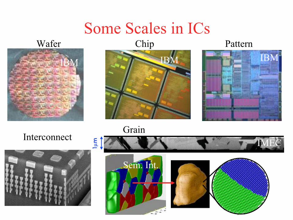
Some Scales in ICsWafer Chip Pattern
InterconnectGrain
IBM IBM IBM
IBM
IMEC
Sem. Int.
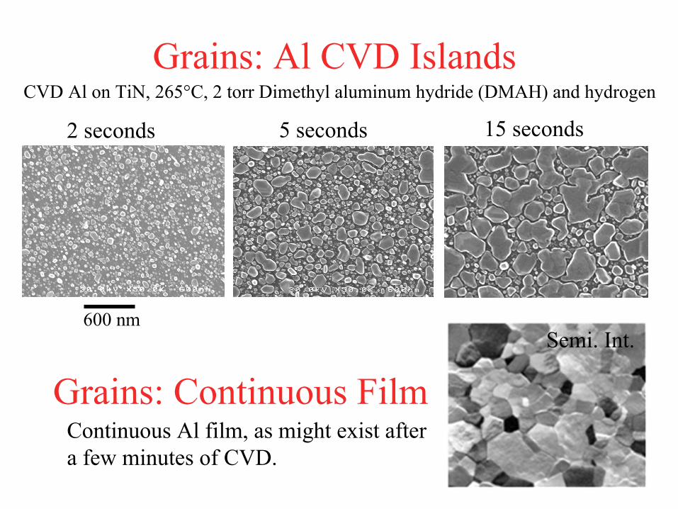
Grains: Al CVD Islands
5 seconds 15 seconds2 seconds
600 nm
CVD Al on TiN, 265°C, 2 torr
Dimethyl
aluminum hydride (DMAH) and hydrogen
Continuous Al film, as might exist after a few minutes of CVD.
Semi. Int.
Grains: Continuous Film
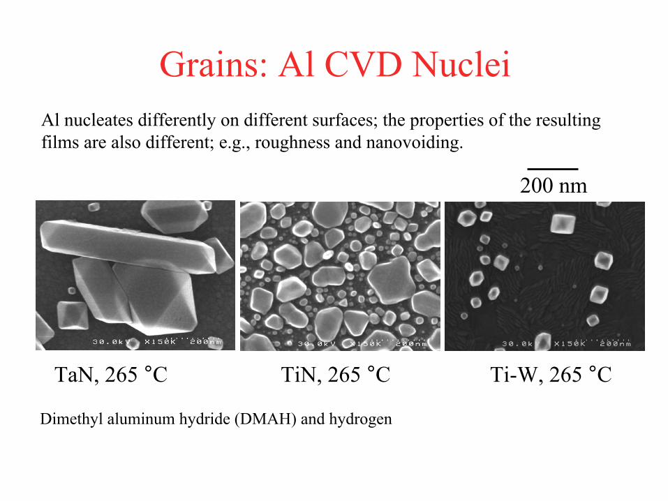
Grains: Al CVD Nuclei
TaN, 265 °C TiN, 265 °C Ti-W, 265 °C
200 nm
Dimethyl
aluminum hydride (DMAH) and hydrogen
Al nucleates differently on different surfaces; the properties of the resulting films are also different; e.g., roughness and nanovoiding.
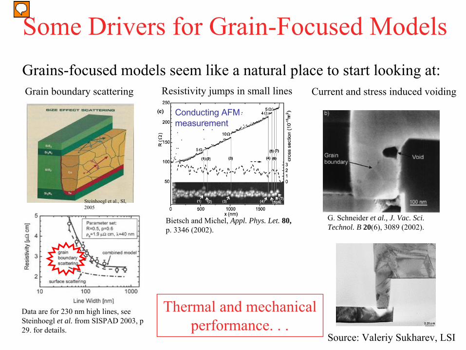
Some Drivers for Grain-Focused Models
Data are for 230 nm high lines, see Steinhoegl
et al. from SISPAD 2003, p 29. for details.
Steinhoegl
et al., SI, 2005
Conducting AFMmeasurementConducting AFMmeasurement
Bietsch
and Michel, Appl. Phys. Let. 80,p. 3346 (2002).
Grains-focused models seem like a natural place to start looking at: Grain boundary scattering Resistivity jumps in small lines
G. Schneider et al., J. Vac. Sci. Technol. B 20(6), 3089 (2002).
Current and stress induced voiding
Source: Valeriy
Sukharev, LSI
Thermal and mechanical performance. . .
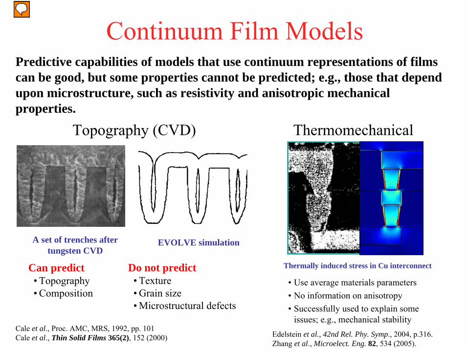
Can predict•
Topography•
Composition
A set of trenches after tungsten CVD
EVOLVE simulation
Do not predict•
Texture•
Grain size•
Microstructural defects
Predictive capabilities of models that use continuum representations of films can be good, but some properties cannot be predicted; e.g., those that depend upon microstructure, such as resistivity and anisotropic mechanical properties.
Continuum Film Models
Cale et al., Proc. AMC, MRS, 1992, pp. 101Cale et al., Thin Solid Films 365(2), 152 (2000)
•
Use average materials parameters •
No information on anisotropy•
Successfully used to explain some issues; e.g., mechanical stability
Thermally induced stress in Cu interconnect
Topography (CVD) Thermomechanical
Edelstein et al., 42nd Rel. Phy. Symp., 2004, p.316.Zhang et al., Microelect. Eng. 82, 534 (2005).
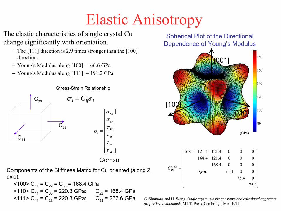
Elastic Anisotropy
C33
C22
C11
Components of the Stiffness Matrix for Cu oriented (along Z axis):
<100> C11
= C22
= C33
= 168.4 GPa<110> C11
= C33
= 220.3 GPa: C22
= 168.4 GPa<111> C11
= C22
= 220.3 GPa: C33
= 237.6 GPa
The elastic characteristics of single crystal Cu change significantly with orientation.
–
The [111] direction is 2.9 times stronger than the [100] direction.
–
Young’s Modulus along [100] = 66.6 GPa–
Young’s Modulus along [111] = 191.2 GPa
Spherical Plot of the Directional Dependence of Young’s Modulus
G. Simmons and H. Wang, Single crystal elastic constants and calculated aggregate properties: a handbook, M.I.T. Press, Cambridge, MA, 1971.
jiji C εσ =
Stress-Strain Relationship
[100][010]
[001]
⎥⎥⎥⎥⎥⎥⎥⎥
⎦
⎤
⎢⎢⎢⎢⎢⎢⎢⎢
⎣
⎡
=
xz
yz
xy
zz
yy
xx
i
τττσσσ
σ
Comsol
⎥⎥⎥⎥⎥⎥⎥⎥
⎦
⎤
⎢⎢⎢⎢⎢⎢⎢⎢
⎣
⎡
=><
4.7504.75004.75.0004.1680004.1214.1680004.1214.1214.168
100
symCijkl
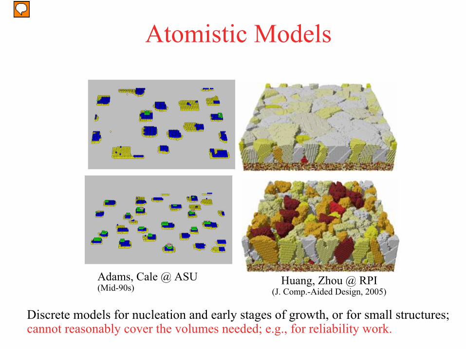
Atomistic Models
Adams, Cale @ ASU(Mid-90s)
Huang, Zhou @ RPI(J. Comp.-Aided Design, 2005)
Discrete models for nucleation and early stages of growth, or for small structures; cannot reasonably cover the volumes needed; e.g., for reliability work.
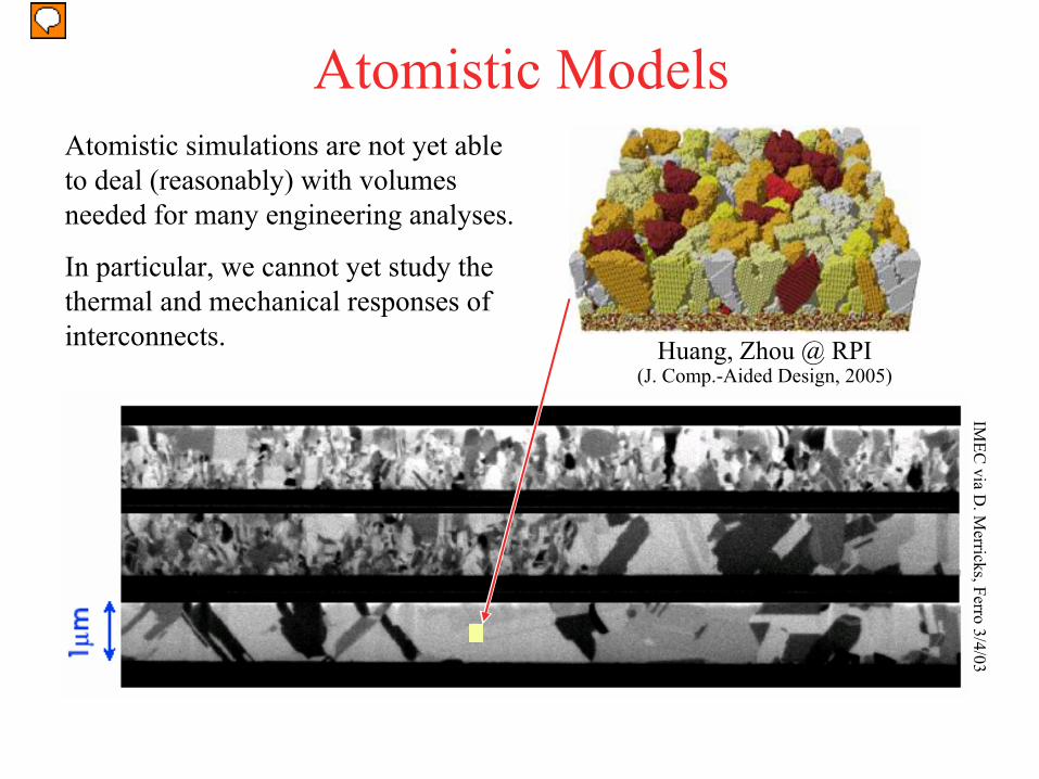
Atomistic ModelsAtomistic simulations are not yet able to deal (reasonably) with volumes needed for many engineering analyses.
In particular, we cannot yet study the thermal and mechanical responses of interconnects.
IMEC
via D. M
erricks, Ferro 3/4/03
Huang, Zhou @ RPI(J. Comp.-Aided Design, 2005)
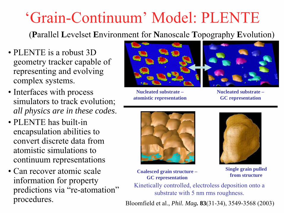
‘Grain-Continuum’
Model: PLENTE
•
PLENTE is a robust 3D geometry tracker capable of representing and evolving complex systems.
•
Interfaces with process simulators to track evolution; all physics are in these codes.
•
PLENTE has built-in encapsulation abilities to convert discrete data from atomistic simulations to continuum representations
•
Can recover atomic scale information for property predictions via “re-atomation”
procedures.
Kinetically controlled, electroless deposition onto a substrate with 5 nm rms roughness.
Coalesced grain structure – GC representation
Single grain pulled from structure
(Parallel Levelset Environment for Nanoscale Topography Evolution)
Bloomfield et al., Phil. Mag. 83(31-34), 3549-3568 (2003)
Nucleated substrate – atomistic representation
Nucleated substrate – GC representation
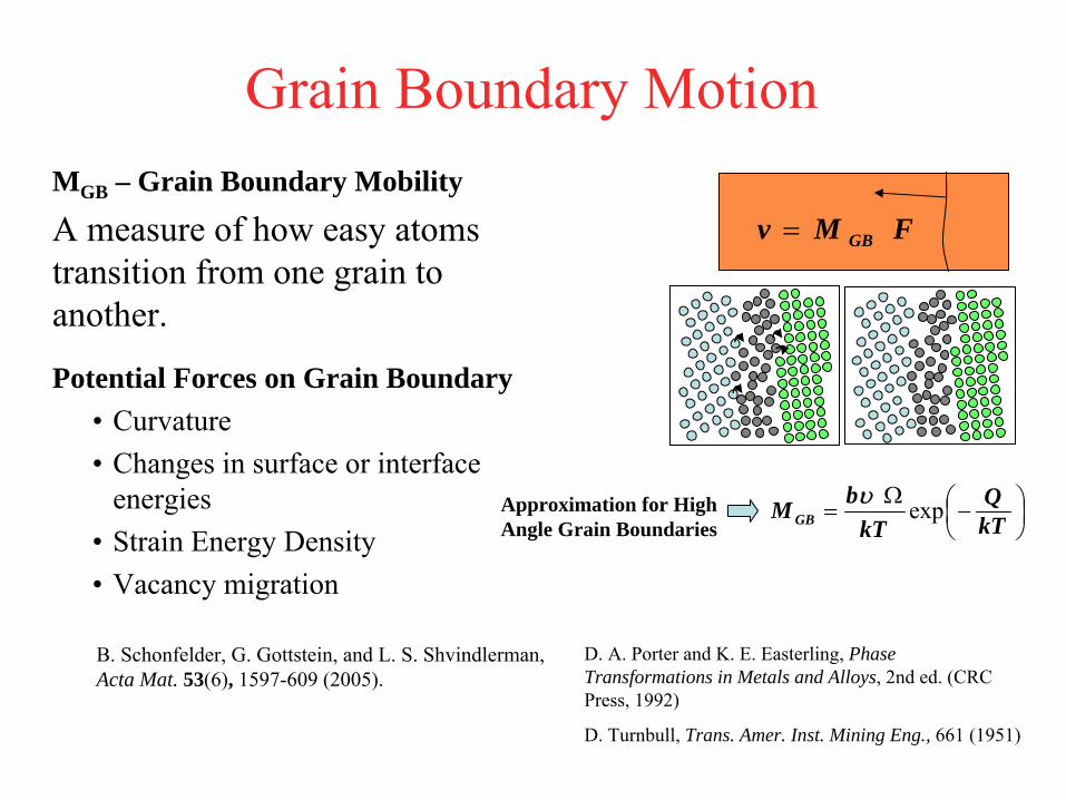
Grain Boundary Motion
Potential Forces on Grain Boundary•
Curvature•
Changes in surface or interface energies
•
Strain Energy Density•
Vacancy migration
FMv GB=
MGB – Grain Boundary Mobility
A measure of how easy atoms transition from one grain to another.
⎟⎠⎞
⎜⎝⎛ −
Ω= kT
QkT
bM GB expυ
D. A. Porter and K. E. Easterling, Phase Transformations in Metals and Alloys, 2nd ed. (CRC Press, 1992)
D. Turnbull, Trans. Amer. Inst. Mining Eng., 661 (1951)
B. Schonfelder, G. Gottstein, and L. S. Shvindlerman, Acta Mat. 53(6), 1597-609 (2005).
Approximation for High Angle Grain Boundaries
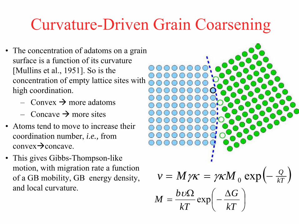
Curvature-Driven Grain Coarsening•
The concentration of adatoms on a grain surface is a function of its curvature [Mullins et al., 1951]. So is the concentration of empty lattice sites with high coordination.
–
Convex more adatoms –
Concave more sites•
Atoms tend to move to increase their coordination number, i.e., from convex concave.
•
This gives Gibbs-Thompson-like motion, with migration rate a function of a GB mobility, GB energy density, and local curvature.
( )kTQMMv −== exp0γκγκ
⎟⎠⎞
⎜⎝⎛ Δ−
Ω=
kTG
kTbM expυ
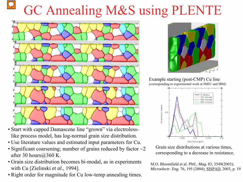
GC Annealing M&S using PLENTE
M.O. Bloomfield et al. Phil., Mag. 83, 3549(2003); Microelectr. Eng. 76, 195 (2004); SISPAD, 2003, p. 19
Example starting (post-CMP) Cu line(corresponding to experimental work at IMEC and IBM)
Grain size distributions at various times, corresponding to a decrease in resistance.
•
Start with capped Damascene line “grown”
via electroless-
like process model, has log-normal grain size distribution.
•
Use literature values and estimated input parameters for Cu.•
Significant coarsening; number of grains reduced by factor ~2 after 30 hours@360 K.
•
Grain size distribution becomes bi-modal, as in experiments with Cu [Zielinski
et al., 1994].•
Right order for magnitude for Cu low-temp annealing times.
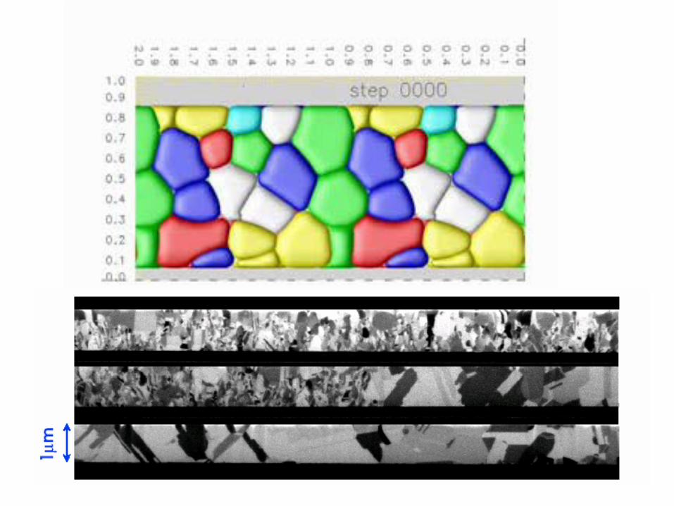
Requisite Movie
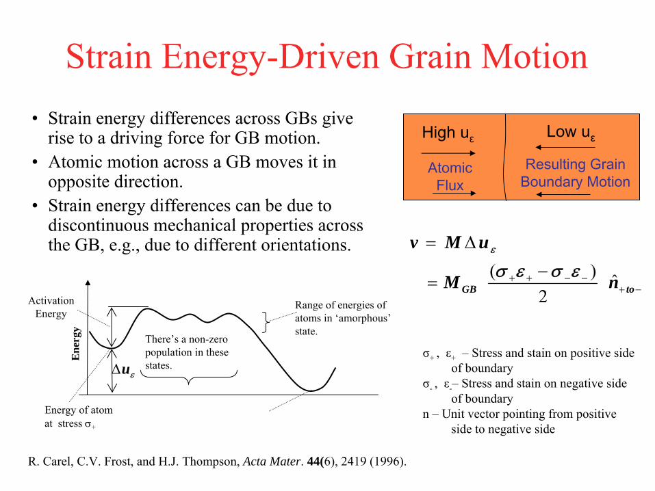
Strain Energy-Driven Grain Motion•
Strain energy differences across GBs
give rise to a driving force for GB motion.
•
Atomic motion across a GB moves it in opposite direction.
•
Strain energy differences can be due to discontinuous mechanical properties across the GB, e.g., due to different orientations.
R. Carel, C.V. Frost, and H.J. Thompson, Acta Mater. 44(6), 2419 (1996).
Resulting Grain Boundary Motion
Atomic
Flux
High uε Low uε
εuMv Δ=
−+−−++ −
= toGB nM ˆ2
)( εσεσ
σ+ , ε+
–
Stress and stain on positive side of boundary
σ-
, ε-
–
Stress and stain on negative side of boundary
n
–
Unit vector pointing from positive side to negative side
There’s a non-zero population in these states.
Ene
rgy
Energy of atom at stress σ+
Range of energies of atoms in ‘amorphous’
state.
ActivationEnergy
εuΔ
2 µm
1 mm
1µm
1µm
Anisotropic Elasticity in Idealized Polycrystalline Films
Insight using thermo-mechanical responses in carefully constructed polycrystalline films.
–
Polycrystalline film is represented as collections of distinct interacting continua each are assigned uniform, material and orientation-dependent parameters (Grain-continuum or GC)
–
Here we study regular hexagonal grains on a silica layer sitting on a silicon wafer.
–
The temperature shifts from 525 K to 425 K.
Fiber textured <111> grains surround a center grain with <100> orientation out of plane of the film
Section of meshdisplaying a single grain
Full Mesh
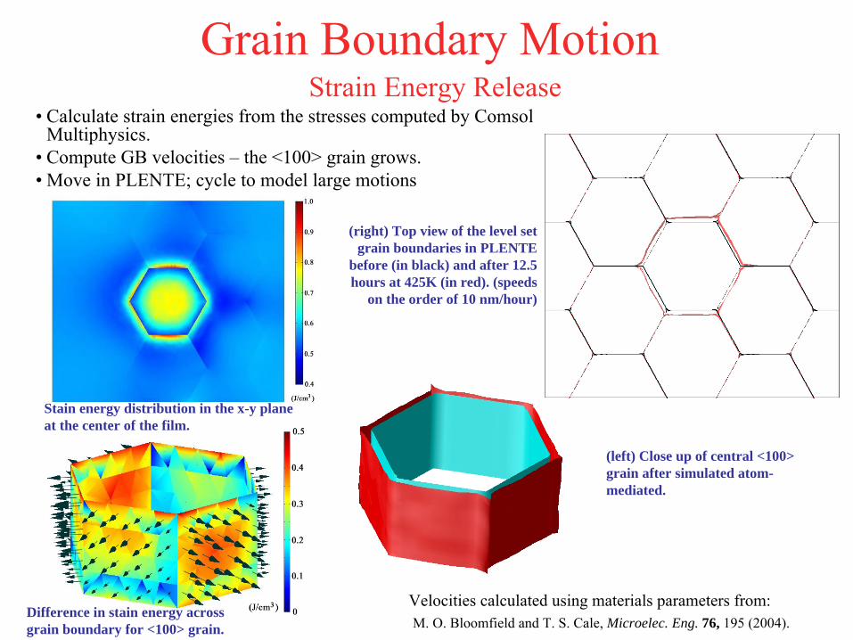
Grain Boundary Motion Strain Energy Release
•
Calculate strain energies from the stresses computed by Comsol Multiphysics.
•
Compute GB velocities –
the <100> grain grows.•
Move in PLENTE; cycle to model large motions
Difference in stain energy across grain boundary for <100> grain.
Stain energy distribution in the x-y plane at the center of the film.
(right) Top view of the level set grain boundaries in PLENTE
before (in black) and after 12.5 hours at 425K (in red). (speeds
on the order of 10 nm/hour)
(left) Close up of central <100> grain after simulated atom- mediated.
Velocities calculated using materials parameters from:M. O. Bloomfield and T. S. Cale, Microelec. Eng. 76, 195 (2004).
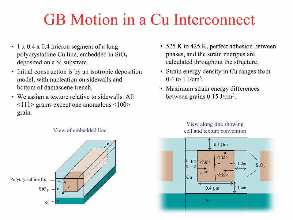
GB Motion in a Cu Interconnect•
1 x 0.4 x 0.4 micron segment of a long polycrystalline Cu line, embedded in SiO2
deposited on a Si substrate.•
Initial construction is by an isotropic deposition model, with nucleation on sidewalls and bottom of damascene trench.
•
We assign a texture relative to sidewalls. All <111> grains except one anomalous <100> grain.
•
525
K to 425
K, perfect adhesion between phases, and the strain energies are calculated throughout the structure.
•
Strain energy density in Cu ranges from 0.4 to 1 J/cm3.
•
Maximum strain energy differences between grains 0.15 J/cm3.
View along line showing
cell and texture convention
SiO2
Cu <hkl>
<hkl>
0.1 μm
0.4 μm
<hkl>
Si
0.1 μm
0.1 μm0.1 μm
Si
SiO2
Polycrystalline Cu
View of embedded line
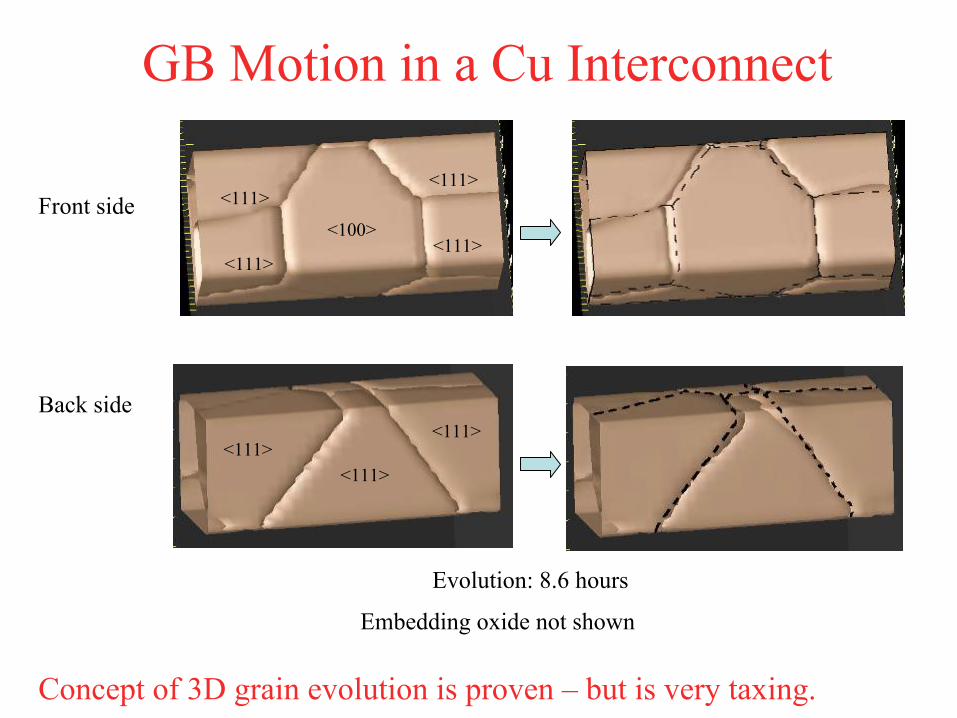
GB Motion in a Cu Interconnect
<111><111>
<111>
<111><111>
<111><111>
<100>
Back side
Front side
Evolution: 8.6 hours
Embedding oxide not shown
Concept of 3D grain evolution is proven –
but is very taxing.
Conclusions•
Advanced models are not all atoms! Grain-
focused models can be an important bridge between continuum and atomistic models–
Can deal with large enough systems to help interpret experimental results from test structures
–
Can incorporate atomistic information (more work needed in this area)
•
Grain-Focused modeling is a new field–
A lot of opportunities for improving our ability to predict reliability, both in terms of data and in terms of materials science in the models.
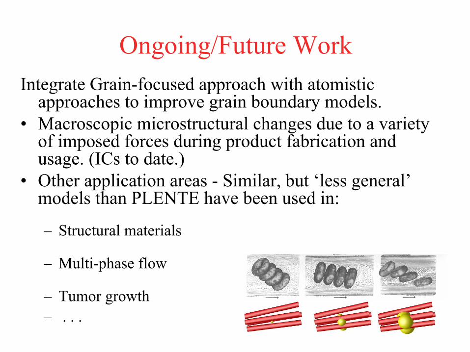
Ongoing/Future WorkIntegrate Grain-focused approach with atomistic
approaches to improve grain boundary models.•
Macroscopic microstructural changes due to a variety of imposed forces during product fabrication and usage. (ICs to date.)
•
Other application areas -
Similar, but ‘less general’ models than PLENTE have been used in:
–
Structural materials
–
Multi-phase flow
–
Tumor growth –
. . .
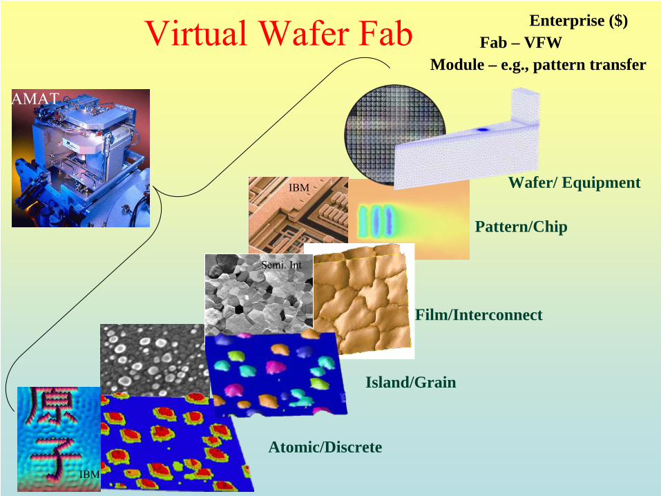
Wafer/ Equipment
Film/Interconnect
Island/Grain
Atomic/Discrete
Fab – VFW
Pattern/Chip
Enterprise ($)Virtual Wafer FabModule – e.g., pattern transfer
IBM
IBM
Semi. Int
AMAT
Thanks!