Embed Size (px)
Citation preview
Virtex-6 FPGA Configurable Logic Block
User Guide
UG364 (v1.2) February 3, 2012
Virtex-6 FPGA CLB User Guide www.xilinx.com UG364 (v1.2) February 3, 2012
Notice of DisclaimerThe information disclosed to you hereunder (the “Materials”) is provided solely for the selection and use of Xilinx products. To the maximum extent permitted by applicable law: (1) Materials are made available "AS IS" and with all faults, Xilinx hereby DISCLAIMS ALL WARRANTIES AND CONDITIONS, EXPRESS, IMPLIED, OR STATUTORY, INCLUDING BUT NOT LIMITED TO WARRANTIES OF MERCHANTABILITY, NON-INFRINGEMENT, OR FITNESS FOR ANY PARTICULAR PURPOSE; and (2) Xilinx shall not be liable (whether in contract or tort, including negligence, or under any other theory of liability) for any loss or damage of any kind or nature related to, arising under, or in connection with, the Materials (including your use of the Materials), including for any direct, indirect, special, incidental, or consequential loss or damage (including loss of data, profits, goodwill, or any type of loss or damage suffered as a result of any action brought by a third party) even if such damage or loss was reasonably foreseeable or Xilinx had been advised of the possibility of the same. Xilinx assumes no obligation to correct any errors contained in the Materials or to notify you of updates to the Materials or to product specifications. You may not reproduce, modify, distribute, or publicly display the Materials without prior written consent. Certain products are subject to the terms and conditions of the Limited Warranties which can be viewed at http://www.xilinx.com/warranty.htm; IP cores may be subject to warranty and support terms contained in a license issued to you by Xilinx. Xilinx products are not designed or intended to be fail-safe or for use in any application requiring fail-safe performance; you assume sole risk and liability for use of Xilinx products in Critical Applications: http://www.xilinx.com/warranty.htm#critapps.
© 2009–2012 Xilinx, Inc. Xilinx, the Xilinx logo, Artix, ISE, Kintex, Spartan, Virtex, Zynq, and other designated brands included herein are trademarks of Xilinx in the United States and other countries. All other trademarks are the property of their respective owners.
Revision HistoryThe following table shows the revision history for this document.
Date Version Revision
06/24/09 1.0 Initial Xilinx release.
09/16/09 1.1 Add Virtex-6 HXT devices to Table 2. Updated discussions at Look-Up Table (LUT), page 11, and Static Read Operation, page 29. CLB labeling change in figures throughout document (Figure 6 through Figure 13, Figure 15, Figure 17, Figure 27 through Figure 29), including clarifying the TDS/TDH functions, descriptions, and notes in Table 7, page 39 and Table 8, page 42.
02/03/12 1.2 In Enable – WE/WED, updated second sentence to say that an inactive write enable prevents writing to memory cells. In Inverting Clock Pins, updated second sentence to “positive edge of the clock.”
Virtex-6 FPGA CLB User Guide www.xilinx.com 3UG364 (v1.2) February 3, 2012
Revision History . . . . . . . . . . . . . . . . . . . . . . . . . . . . . . . . . . . . . . . . . . . . . . . . . . . . . . . . . . . . . 2
Preface: About This GuideAdditional Documentation . . . . . . . . . . . . . . . . . . . . . . . . . . . . . . . . . . . . . . . . . . . . . . . . . . . 5Additional Support Resources . . . . . . . . . . . . . . . . . . . . . . . . . . . . . . . . . . . . . . . . . . . . . . . . 6
Virtex-6 FPGA CLBCLB Overview . . . . . . . . . . . . . . . . . . . . . . . . . . . . . . . . . . . . . . . . . . . . . . . . . . . . . . . . . . . . . . . 7
Slice Description . . . . . . . . . . . . . . . . . . . . . . . . . . . . . . . . . . . . . . . . . . . . . . . . . . . . . . . . . . . 8CLB / Slice Timing Models . . . . . . . . . . . . . . . . . . . . . . . . . . . . . . . . . . . . . . . . . . . . . . . . . . 34
General Slice Timing Model and Parameters . . . . . . . . . . . . . . . . . . . . . . . . . . . . . . . . . 34Slice Distributed RAM Timing Model and Parameters (Available in SLICEM only) 38Slice SRL Timing Model and Parameters (Available in SLICEM only) . . . . . . . . . . . . 41Slice Carry-Chain Timing Model and Parameters . . . . . . . . . . . . . . . . . . . . . . . . . . . . . 44
CLB Primitives . . . . . . . . . . . . . . . . . . . . . . . . . . . . . . . . . . . . . . . . . . . . . . . . . . . . . . . . . . . . . . 45Distributed RAM Primitives . . . . . . . . . . . . . . . . . . . . . . . . . . . . . . . . . . . . . . . . . . . . . . . 45Shift Registers (SRLs) Primitive . . . . . . . . . . . . . . . . . . . . . . . . . . . . . . . . . . . . . . . . . . . . . 47Other Shift Register Applications . . . . . . . . . . . . . . . . . . . . . . . . . . . . . . . . . . . . . . . . . . . 48Multiplexer Primitives . . . . . . . . . . . . . . . . . . . . . . . . . . . . . . . . . . . . . . . . . . . . . . . . . . . . 49Carry Chain Primitive . . . . . . . . . . . . . . . . . . . . . . . . . . . . . . . . . . . . . . . . . . . . . . . . . . . . . 49
Table of Contents
Virtex-6 FPGA CLB User Guide www.xilinx.com 5UG364 (v1.2) February 3, 2012
Preface
About This Guide
This guide serves as a technical reference describing the Virtex®-6 FPGA configurable logic blocks (CLBs). Usually, the logic synthesis software assigns the CLB resources without system designer intervention. It can be advantageous for the designer to understand certain CLB details, including the varying capabilities of the look-up tables (LUTs), the physical direction of the carry propagation, the number and distribution of the available flip-flops, and the availability of the very efficient shift registers. This guide describes these and other features of the CLB in detail.
Additional DocumentationThe following documents are also available for download at http://www.xilinx.com/support/documentation/virtex-6.htm.
• Virtex-6 Family Overview
The features and product selection of the Virtex-6 family are outlined in this overview.
• Virtex-6 FPGA Data Sheet: DC and Switching Characteristics
This data sheet contains the DC and Switching Characteristic specifications for the Virtex-6 family.
• Virtex-6 FPGA Packaging and Pinout Specifications
This specification includes the tables for device/package combinations and maximum I/Os, pin definitions, pinout tables, pinout diagrams, mechanical drawings, and thermal specifications.
• Virtex-6 FPGA Configuration Guide
This all-encompassing configuration guide includes chapters on configuration interfaces (serial and SelectMAP), bitstream encryption, boundary-scan and JTAG configuration, reconfiguration techniques, and readback through the SelectMAP and JTAG interfaces.
• Virtex-6 FPGA Clocking Resources User Guide
This guide describes the clocking resources available in all Virtex-6 devices, including the MMCM and PLLs.
• Virtex-6 FPGA Memory Resources User Guide
The functionality of the block RAM and FIFO are described in this user guide.
• Virtex-6 FPGA SelectIO Resources User Guide
This guide describes the SelectIO™ resources available in all Virtex-6 devices.
6 www.xilinx.com Virtex-6 FPGA CLB User GuideUG364 (v1.2) February 3, 2012
Preface: About This Guide
• Virtex-6 FPGA GTH Transceivers User Guide
This guide describes the GTH transceivers available in all Virtex-6 HXT FPGAs except the XC6VHX250T and the XC6VHX380T in the FF1154 package..
• Virtex-6 FPGA GTX Transceivers User Guide
This guide describes the GTX transceivers available in all Virtex-6 FPGAs except the XC6VLX760.
• Virtex-6 FPGA Embedded Tri-Mode Ethernet MAC User Guide
This guide describes the dedicated Tri-Mode Ethernet Media Access Controller available in all Virtex-6 FPGAs except the XC6VLX760.
• Virtex-6 FPGA DSP48E1 Slice User Guide
This guide describes the architecture of the DSP48E1 slice in Virtex-6 FPGAs and provides configuration examples.
• Virtex-6 FPGA System Monitor User Guide
The System Monitor functionality available in all Virtex-6 devices is outlined in this guide.
• Virtex-6 FPGA PCB Design Guide
This guide provides information on PCB design for Virtex-6 devices, with a focus on strategies for making design decisions at the PCB and interface level.
Additional Support ResourcesTo search the database of silicon and software questions and answers or to create a technical support case in WebCase, see the Xilinx website at:
http://www.xilinx.com/support.
Virtex-6 FPGA CLB User Guide www.xilinx.com 7UG364 (v1.2) February 3, 2012
Virtex-6 FPGA CLB
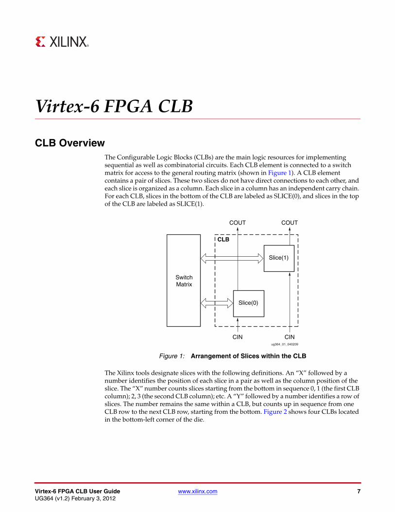
CLB OverviewThe Configurable Logic Blocks (CLBs) are the main logic resources for implementing sequential as well as combinatorial circuits. Each CLB element is connected to a switch matrix for access to the general routing matrix (shown in Figure 1). A CLB element contains a pair of slices. These two slices do not have direct connections to each other, and each slice is organized as a column. Each slice in a column has an independent carry chain. For each CLB, slices in the bottom of the CLB are labeled as SLICE(0), and slices in the top of the CLB are labeled as SLICE(1).
The Xilinx tools designate slices with the following definitions. An “X” followed by a number identifies the position of each slice in a pair as well as the column position of the slice. The “X” number counts slices starting from the bottom in sequence 0, 1 (the first CLB column); 2, 3 (the second CLB column); etc. A “Y” followed by a number identifies a row of slices. The number remains the same within a CLB, but counts up in sequence from one CLB row to the next CLB row, starting from the bottom. Figure 2 shows four CLBs located in the bottom-left corner of the die.
X-Ref Target - Figure 1
Figure 1: Arrangement of Slices within the CLB
SwitchMatrix
Slice(1)
COUTCOUT
CINCIN
Slice(0)
CLB
ug364_01_040209

8 www.xilinx.com Virtex-6 FPGA CLB User GuideUG364 (v1.2) February 3, 2012
CLB Overview
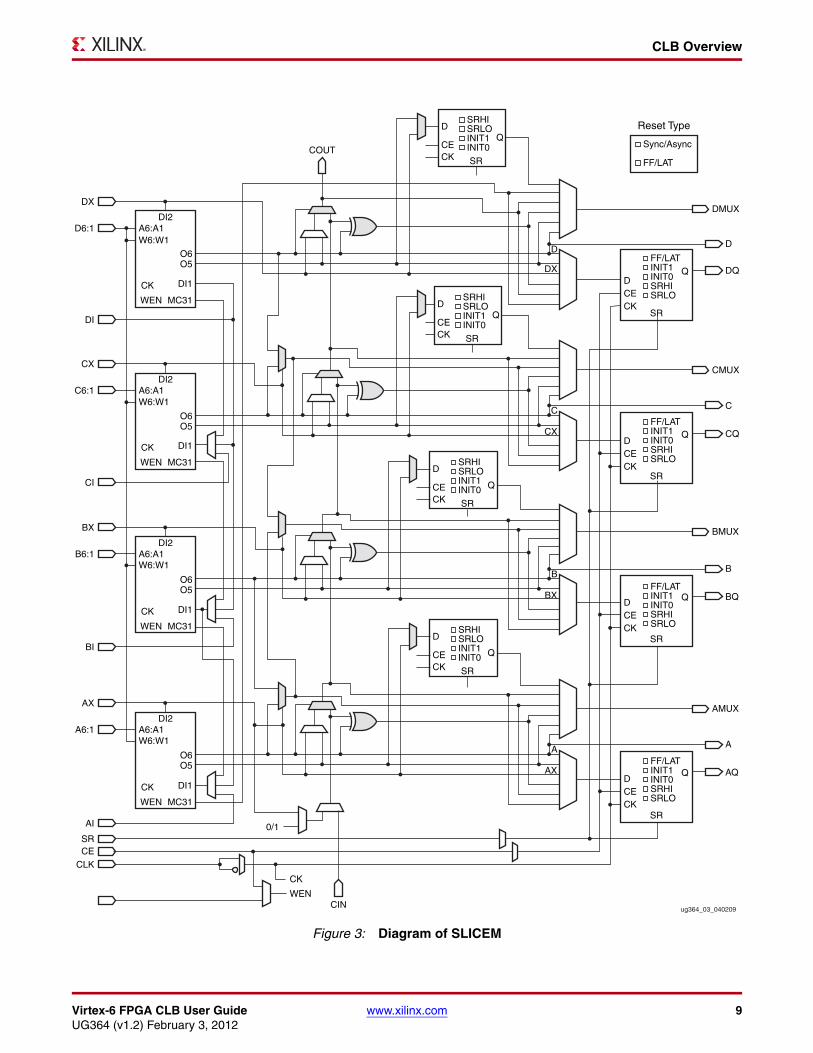
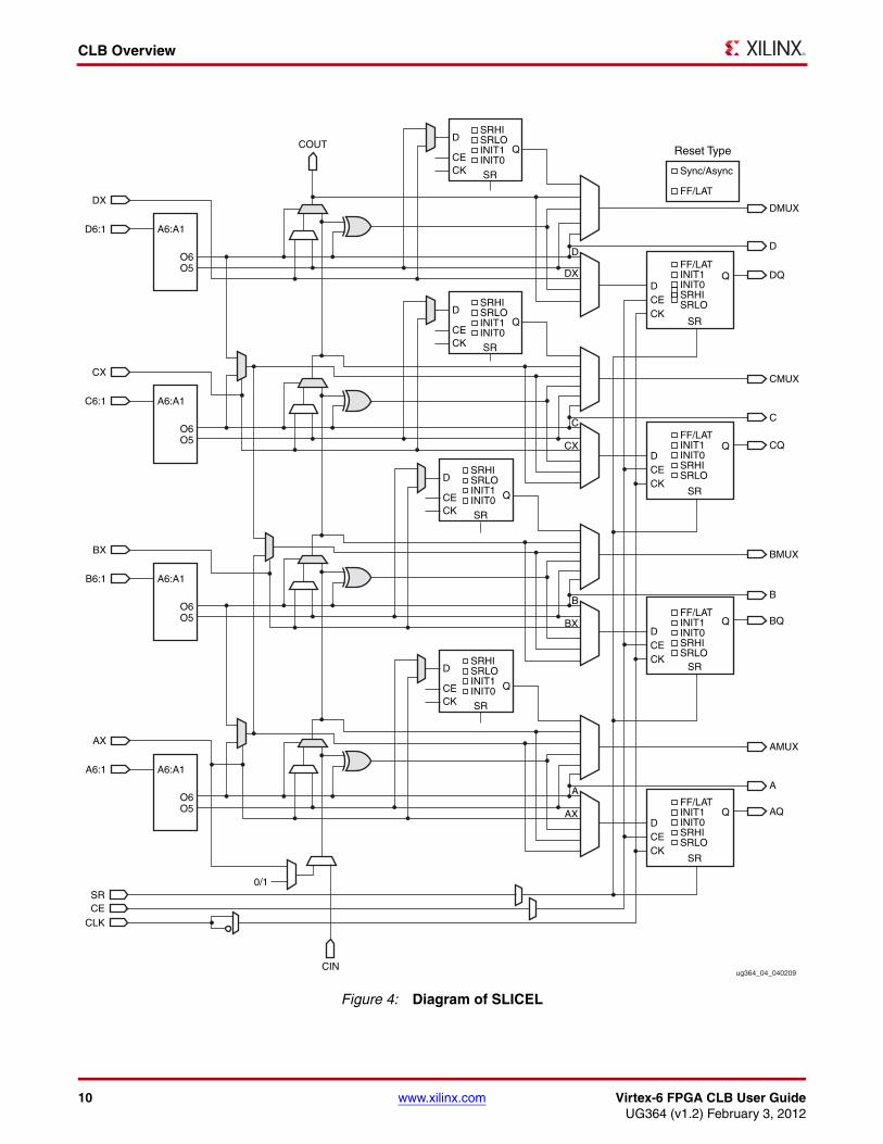
Slice DescriptionEvery slice contains four logic-function generators (or look-up tables), eight storage elements, wide-function multiplexers, and carry logic. These elements are used by all slices to provide logic, arithmetic, and ROM functions. In addition to this, some slices support two additional functions: storing data using distributed RAM and shifting data with 32-bit registers. Slices that support these additional functions are called SLICEM; others are called SLICEL. SLICEM (shown in Figure 3) represents a superset of elements and connections found in all slices. SLICEL is shown in Figure 4.
Each CLB can contain zero or one SLICEM. Every other CLB column contains a SLICEMs. In addition, the two CLB columns to the left of the DSP48E columns both contain a SLICEL and a SLICEM.
X-Ref Target - Figure 2
Figure 2: Row and Column Relationship between CLBs and Slices
SliceX1Y1
COUTCOUT
CINCIN
SliceX0Y1
CLB
ug364_02_040209
SliceX1Y0
COUTCOUT
SliceX0Y0
CLB
SliceX3Y1
COUTCOUT
CINCIN
SliceX2Y1
CLB
SliceX3Y0
COUTCOUT
SliceX2Y0
CLB
Virtex-6 FPGA CLB User Guide www.xilinx.com 9UG364 (v1.2) February 3, 2012
CLB Overview
X-Ref Target - Figure 3
Figure 3: Diagram of SLICEM
A6:A1
D
COUT
D
DX
C
CX
B
BX
A
AX
O6
DI2
O5
DI1
MC31WEN
CK
DI1
MC31WEN
CK
DI1
MC31WEN
CK
DI1
MC31WEN
CK
ug364_03_040209
DXDMUX
D
DQ
C
CQ
CMUX
B
BQ
BMUX
A
AQ
AMUX
Reset Type
D
FF/LATINIT1INIT0SRHISRLO
SR
CECK
FF/LATINIT1INIT0SRHISRLO
FF/LATINIT1INIT0SRHISRLO
FF/LATINIT1INIT0SRHISRLO
D
SR
CECK
D
SR
CECK
D
SR
Q
CECK
CIN
0/1
WEN
CK
Sync/Async
FF/LAT
A6:A1
O6O5
C6:1
CX
D6:1
DI
A6:A1
O6O5
B6:1
BX
A6:A1W6:W1
W6:W1
W6:W1
W6:W1
O6O5
A6:1
AX
SRCE
CLK
CEQ
CK SR
Q
Q
Q
SRHISRLOINIT1INIT0
D
CEQ
CK SR
SRHISRLOINIT1INIT0
D
CE Q
CK SR
SRHISRLOINIT1INIT0
D
CE Q
CK SR
SRHISRLOINIT1INIT0
DI2
DI2
DI2
CI
BI
AI
10 www.xilinx.com Virtex-6 FPGA CLB User GuideUG364 (v1.2) February 3, 2012
CLB Overview
X-Ref Target - Figure 4
Figure 4: Diagram of SLICEL
A6:A1
DCOUT
D
DX
C
CX
B
BX
A
AX
O6O5
ug364_04_040209
DXDMUX
D
DQ
C
CQ
CMUX
B
BQ
BMUX
A
AQ
AMUX
Reset Type
D
FF/LATINIT1INIT0SRHISRLO
SR
CECK
FF/LATINIT1INIT0SRHISRLO
FF/LATINIT1INIT0SRHISRLO
FF/LATINIT1INIT0SRHISRLO
D
SR
CECK
D
SR
CECK
D
SR
Q
CECK
CIN
0/1
Sync/Async
FF/LAT
A6:A1
O6O5
C6:1
CX
D6:1
A6:A1
O6O5
B6:1
BX
A6:A1
O6O5
A6:1
AX
SRCE
CLK
CEQ
CK SR
Q
Q
Q
SRHISRLOINIT1INIT0
D
CEQ
CK SR
SRHISRLOINIT1INIT0
D
CE Q
CK SR
SRHISRLOINIT1INIT0
D
CE Q
CK SR
SRHISRLOINIT1INIT0

Virtex-6 FPGA CLB User Guide www.xilinx.com 11UG364 (v1.2) February 3, 2012
CLB Overview
CLB/Slice Configurations
Table 1 summarizes the logic resources in one CLB. Each CLB or slice can be implemented in one of the configurations listed. Table 2 shows the available resources in all CLBs.
Look-Up Table (LUT)
The function generators in Virtex-6 FPGAs are implemented as six-input look-up tables (LUTs). There are six independent inputs (A inputs - A1 to A6) and two independent outputs (O5 and O6) for each of the four function generators in a slice (A, B, C, and D). The function generators can implement any arbitrarily defined six-input Boolean function. Each function generator can also implement two arbitrarily defined five-input Boolean functions, as long as these two functions share common inputs. Only the O6 output of the function generator is used when a six-input function is implemented. Both O5 and O6 are used for each of the five-input function generators implemented. In this case, A6 is driven High by the software. The propagation delay through a LUT is independent of the function implemented, or whether one six-input or two five-input generators are implemented. Signals from the function generators can exit the slice (through A, B, C, D output for O6 or AMUX, BMUX, CMUX, DMUX output for O5), enter the XOR dedicated gate from an O6 output (see Fast Lookahead Carry Logic), enter the carry-logic chain from an O5 output (see Fast Lookahead Carry Logic), enter the select line of the carry-logic multiplexer from
Table 1: Logic Resources in One CLB
Slices LUTs Flip-FlopsArithmetic and Carry Chains
Distributed RAM(1) Shift Registers(1)
2 8 16 2 256 bits 128 bits
Notes: 1. SLICEM only, SLICEL does not have distributed RAM or shift registers.
Table 2: Virtex-6 FPGA Logic Resources Available in All CLBs
DeviceTotal
SlicesSLICELs SLICEMs
Number of 6-Input LUTs
Maximum Distributed RAM (Kb)
Shift Register (Kb)
Number of Flip-Flops
XC6VLX75T 11,640 7,460 4,180 46,560 1,045 522.5 93,120
XC6VLX130T 20,000 13,040 6,960 80,000 1,740 870 160,000
XC6VLX195T 31,200 19,040 12,160 124,800 3,140 1,570 249,600
XC6VLX240T 37,680 23,080 14,600 150,720 3,770 1,885 301,440
XC6VLX365T 56,880 40,360 16,520 227,520 4,130 2,065 455,040
XC6VLX550T 85,920 61,120 24,800 343,680 6,200 3,100 687,360
XC6VLX760 118,560 85,440 33,120 474,240 8,280 4,140 948,480
XC6VSX315T 49,200 28,840 20,360 196,800 5,090 2,545 393,600
XC6VSX475T 74,400 48,840 30,560 297,600 7,640 3,820 595,200
XC6VHX250T 39,360 27,200 12,160 157,440 3,040 1,520 314,880
XC6VHX255T 39,600 27,400 12,200 158,400 3,050 1,525 316,800
XC6VHX380T 59,760 41,520 18,240 239,040 4,570 2,285 478,080
XC6VHX565T 88,560 63,080 25,480 354,240 6,370 3,185 708,480

12 www.xilinx.com Virtex-6 FPGA CLB User GuideUG364 (v1.2) February 3, 2012
CLB Overview
O6 output (see Fast Lookahead Carry Logic), feed the D input of the storage element, or go to F7AMUX/F7BMUX from O6 output.
In addition to the basic LUTs, slices contain three multiplexers (F7AMUX, F7BMUX, and F8MUX). These multiplexers are used to combine up to four function generators to provide any function of seven or eight inputs in a slice. F7AMUX and F7BMUX are used to generate seven input functions from LUTs A and B, or C and D, while F8MUX is used to combine all LUTs to generate eight input functions. Functions with more than eight inputs can be implemented using multiple slices. There are no direct connections between slices to form function generators greater than eight inputs within a CLB.
Storage Elements
As in previous Virtex architectures, there are four (original) storage elements in a slice that can be configured as either edge-triggered D-type flip-flops or level-sensitive latches. The D input can be driven directly by a LUT output via AFFMUX, BFFMUX, CFFMUX or DFFMUX, or by the BYPASS slice inputs bypassing the function generators via AX, BX, CX, or DX input. When configured as a latch, the latch is transparent when the CLK is Low.
In Virtex-6 devices, there are now four additional storage elements that can only be configured as edge-triggered D-type flip-flops. The D input can be driven by the O5 output of the LUT or the BYPASS slice inputs via AX, BX, CX, or DX input. When the original 4 storage elements are configured as latches, these 4 additional storage elements can not be used.
The control signals clock (CLK), clock enable (CE), and set/reset (SR) are common to all storage elements in one slice. When one flip-flop in a slice has SR or CE enabled, the other flip-flops used in the slice will also have SR or CE enabled by the common signal. Only the CLK signal has independent polarity. Any inverter placed on the clock signal is automatically absorbed. The CE and SR signals are active High. All flip-flop and latch primitives have CE and non-CE versions.
The SR signal forces the storage element into the state specified by the attribute SRHIGH or SRLOW. SRHIGH forces a logic High at the storage element output when SR is asserted, while SRLOW forces a logic Low at the storage element output (see Table 3).
Figure 5 shows both the register only and the register/latch configuration in a slice.
Table 3: Truth Table when using SRLOW and SRHIGH
SR SRVAL Function
0 SRLOW (default) No Logic Change
1 SRLOW (default) 0
0 SRHIGH No Logic Change
1 SRHIGH 1

Virtex-6 FPGA CLB User Guide www.xilinx.com 13UG364 (v1.2) February 3, 2012
CLB Overview
SRHIGH and SRLOW can be set individually for each storage element in a slice. The choice of synchronous (SYNC) or asynchronous (ASYNC) set/reset (SRTYPE) cannot be set individually for each storage element in a slice.
The initial state after configuration or global initial state is defined by separate INIT0 and INIT1 attributes. By default, setting the SRLOW attribute sets INIT0, and setting the SRHIGH attribute sets INIT1. Virtex-6 devices can set INIT0 and INIT1 independent of SRHIGH and SRLOW.
The configuration options for the set and reset functionality of a register or the four storage elements capable of functioning as a latch are as follows:
• No set or reset
• Synchronous set
• Synchronous reset
• Asynchronous set (preset)
• Asynchronous reset (clear)
X-Ref Target - Figure 5
Figure 5: Two Versions of Configuration in a Slice: 4 Registers Only and 4 Register/Latch
ug364_05_040209
DX
CX
BX
CE
AX
DQ
CQ
BQ
AQ
D
FFLATCHINIT1INIT0SRHIGHSRLOWSR
DFF/LATCHLUT D Output
LUT C Output
CECK
D
FFLATCHINIT1INIT0SRHIGHSRLOWSR
CECK
D
FFLATCHINIT1INIT0SRHIGHSRLOWSR
CECK
D
FFLATCHINIT1INIT0SRHIGHSRLOWSR
Q
CECK
Q
Q
Q
SR
LUT B Output
LUT A Output AFF/LATCH
BFF/LATCH
CFF/LATCH
CLK
Reset Type
Sync
Async
DX
CX
BX
CE
AX
DQ
CQ
BQ
AQ
D
SR
DFFLUT D O5 Output
LUT C O5 Output
CECK
INIT1INIT0SRHIGHSRLOW
INIT1INIT0SRHIGHSRLOW
INIT1INIT0SRHIGHSRLOW
INIT1INIT0SRHIGHSRLOW
D
SR
CECK
D
SR
CECK
D
SR
Q
CECK
Q
Q
Q
SR
LUT B O5 Output
LUT A O5 Output AFF
BFF
CFF
CLK
Reset Type
Sync
Async
14 www.xilinx.com Virtex-6 FPGA CLB User GuideUG364 (v1.2) February 3, 2012
CLB Overview
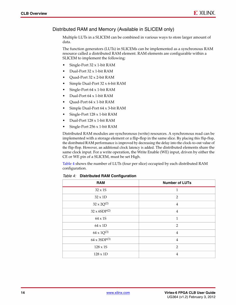
Distributed RAM and Memory (Available in SLICEM only)
Multiple LUTs in a SLICEM can be combined in various ways to store larger amount of data.
The function generators (LUTs) in SLICEMs can be implemented as a synchronous RAM resource called a distributed RAM element. RAM elements are configurable within a SLICEM to implement the following:
• Single-Port 32 x 1-bit RAM
• Dual-Port 32 x 1-bit RAM
• Quad-Port 32 x 2-bit RAM
• Simple Dual-Port 32 x 6-bit RAM
• Single-Port 64 x 1-bit RAM
• Dual-Port 64 x 1-bit RAM
• Quad-Port 64 x 1-bit RAM
• Simple Dual-Port 64 x 3-bit RAM
• Single-Port 128 x 1-bit RAM
• Dual-Port 128 x 1-bit RAM
• Single-Port 256 x 1-bit RAM
Distributed RAM modules are synchronous (write) resources. A synchronous read can be implemented with a storage element or a flip-flop in the same slice. By placing this flip-flop, the distributed RAM performance is improved by decreasing the delay into the clock-to-out value of the flip-flop. However, an additional clock latency is added. The distributed elements share the same clock input. For a write operation, the Write Enable (WE) input, driven by either the CE or WE pin of a SLICEM, must be set High.
Table 4 shows the number of LUTs (four per slice) occupied by each distributed RAM configuration.
Table 4: Distributed RAM Configuration
RAM Number of LUTs
32 x 1S 1
32 x 1D 2
32 x 2Q(2) 4
32 x 6SDP(2) 4
64 x 1S 1
64 x 1D 2
64 x 1Q(3) 4
64 x 3SDP(3) 4
128 x 1S 2
128 x 1D 4

Virtex-6 FPGA CLB User Guide www.xilinx.com 15UG364 (v1.2) February 3, 2012
CLB Overview
For single-port configurations, distributed RAM has a common address port for synchronous writes and asynchronous reads. For dual-port configurations, distributed RAM has one port for synchronous writes and asynchronous reads, and another port for asynchronous reads. In simple dual-port configuration, there is no data out (read port) from the write port. For quad-port configurations, distributed RAM has one port for synchronous writes and asynchronous reads, and three additional ports for asynchronous reads.
In single-port mode, read and write addresses share the same address bus. In dual-port mode, one function generator is connected with the shared read and write port address. The second function generator has the A inputs connected to a second read-only port address and the WA inputs shared with the first read/write port address.
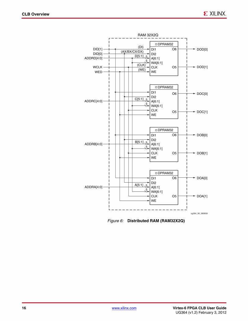
Figure 6 through Figure 14 illustrate various example distributed RAM configurations occupying one SLICEM. When using x2 configuration (RAM32X2Q), A6 and WA6 are driven High by the software to keep O5 and O6 independent.
256 x 1S 4
Notes: 1. S = single-port configuration; D = dual-port configuration; Q = quad-port configuration; SDP = simple
dual-port configuration.2. RAM32M is the associated primitive for this configuration.3. RAM64M is the associated primitive for this configuration.
Table 4: Distributed RAM Configuration (Cont’d)
RAM Number of LUTs
16 www.xilinx.com Virtex-6 FPGA CLB User GuideUG364 (v1.2) February 3, 2012
CLB Overview
X-Ref Target - Figure 6
Figure 6: Distributed RAM (RAM32X2Q)
ug364_06_080609
DI1 DOD[0]
DOC[0]
DOD[1]
DOC[1]
DOB[0]
DOB[1]
DOA[0]
DOA[1]
DI2
DID[1]DID[0]
ADDRD[4:0]
ADDRC[4:0]
ADDRB[4:0]
ADDRA[4:0]
WCLK
WED
(CLK)
(WE)
5
5
DPRAM32
RAM 32X2Q
A[6:1]WA[6:1]CLKWE
O6
O5
DI1DI2
5
5
DPRAM32
A[6:1]WA[6:1]CLKWE
O6
DI1DI2
DI2
B[5:1]
C[5:1]
D[5:1](AX/BX/CX/DX)
(DI)
A[5:1]
5
5
DPRAM32
A[6:1]WA[6:1]CLKWE
O6
DI1
5
5
DPRAM32
A[6:1]WA[6:1]CLKWE
O6
O5
O5
O5
Virtex-6 FPGA CLB User Guide www.xilinx.com 17UG364 (v1.2) February 3, 2012
CLB Overview
X-Ref Target - Figure 7
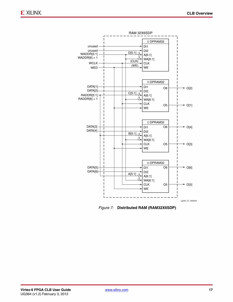
Figure 7: Distributed RAM (RAM32X6SDP)
ug364_07_080609
DI1
O[2]
O[1]
O[4]
O[3]
O[6]
O[5]
DI2
unusedunused
WADDR[5:1]WADDR[6] = 1
RADDR[5:1]RADDR[6] = 1
DATA[1]DATA[2]
DATA[3]DATA[4]
DATA[5]DATA[6]
WCLK
WED
(CLK)
(WE)
5
5
DPRAM32
RAM 32X6SDP
A[6:1]WA[6:1]CLKWE
DI1DI2
5
5
DPRAM32
A[6:1]WA[6:1]CLKWE
O6
DI1DI2
DI2
B[5:1]
C[5:1]
D[5:1]
A[5:1]
5
5
DPRAM32
A[6:1]WA[6:1]CLKWE
O6
DI1
5
5
DPRAM32
A[6:1]WA[6:1]CLKWE
O6
O5
O5
O5
18 www.xilinx.com Virtex-6 FPGA CLB User GuideUG364 (v1.2) February 3, 2012
CLB Overview
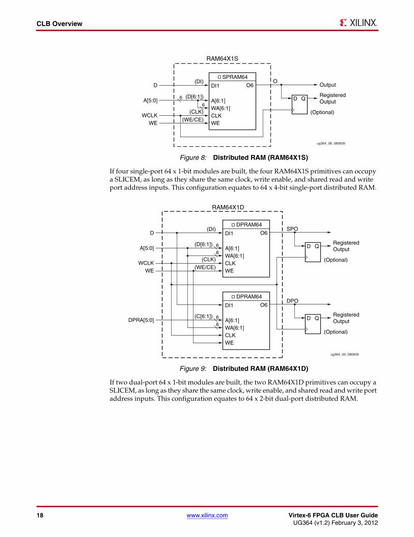
If four single-port 64 x 1-bit modules are built, the four RAM64X1S primitives can occupy a SLICEM, as long as they share the same clock, write enable, and shared read and write port address inputs. This configuration equates to 64 x 4-bit single-port distributed RAM.
If two dual-port 64 x 1-bit modules are built, the two RAM64X1D primitives can occupy a SLICEM, as long as they share the same clock, write enable, and shared read and write port address inputs. This configuration equates to 64 x 2-bit dual-port distributed RAM.
X-Ref Target - Figure 8
Figure 8: Distributed RAM (RAM64X1S)
X-Ref Target - Figure 9
Figure 9: Distributed RAM (RAM64X1D)
ug364_08_080609
Output
RegisteredOutput
(Optional)
DI1
D Q
(DI)D
A[5:0]
WCLKWE
(D[6:1])
(CLK)
(WE/CE)
6
SPRAM64
RAM64X1S
A[6:1]WA[6:1]CLKWE
O6O
6
ug364_09_080609
DI1(DI)
D
A[5:0]
WCLKWE
(D[6:1])
(CLK)
(WE/CE)
6
6
DPRAM64
RAM64X1D
A[6:1]WA[6:1]CLKWE
O6
DI1
DPRA[5:0](C[6:1]) 6
6
DPRAM64
A[6:1]WA[6:1]CLKWE
O6
RegisteredOutput
(Optional)
D Q
SPO
RegisteredOutput
(Optional)
D Q
DPO

Virtex-6 FPGA CLB User Guide www.xilinx.com 19UG364 (v1.2) February 3, 2012
CLB Overview
X-Ref Target - Figure 10
Figure 10: Distributed RAM (RAM64X1Q)
ug364_10_080609
DI1DID
ADDRD
ADDRC
ADDRB
ADDRA
WCLK
WE
(CLK)
(WE)
DPRAM64
RAM64X1Q
A[6:1]WA[6:1]CLKWE
O6
DI1
DPRAM64
A[6:1]WA[6:1]CLKWE
O6
DI1
(B[6:1])
(C[6:1])
(D[6:1])
(DI)
(A[6:1])
DPRAM64
A[6:1]WA[6:1]CLKWE
O6
DI1
DPRAM64
A[6:1]WA[6:1]CLKWE
O6
RegisteredOutput
DOD
DOC
DOB
DOA
(Optional)
D Q
RegisteredOutput
(Optional)
D Q
RegisteredOutput
(Optional)
D Q
RegisteredOutput
(Optional)
D Q
20 www.xilinx.com Virtex-6 FPGA CLB User GuideUG364 (v1.2) February 3, 2012
CLB Overview
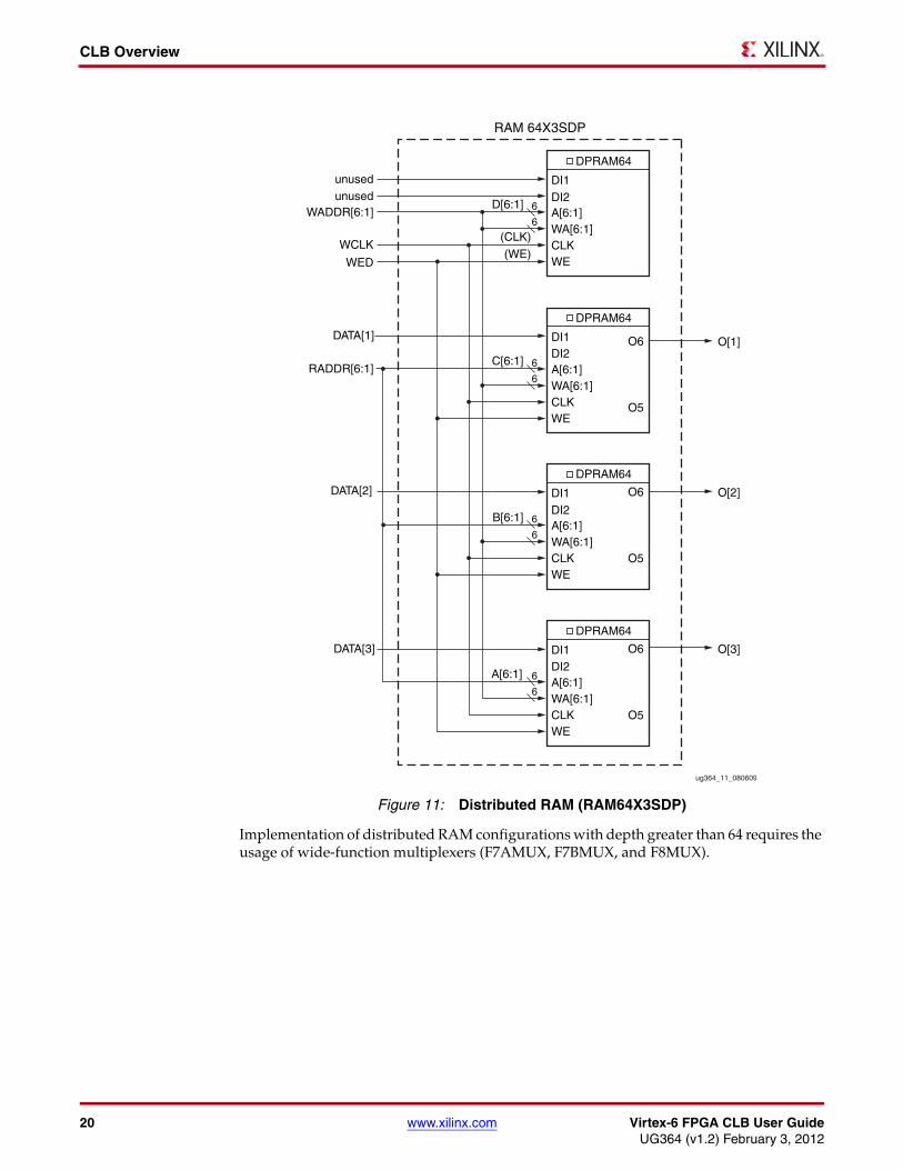
Implementation of distributed RAM configurations with depth greater than 64 requires the usage of wide-function multiplexers (F7AMUX, F7BMUX, and F8MUX).
X-Ref Target - Figure 11
Figure 11: Distributed RAM (RAM64X3SDP)
ug364_11_080609
DI1
O[1]
O[2]
O[3]
DI2
unusedunused
WADDR[6:1]
RADDR[6:1]
DATA[1]
DATA[2]
DATA[3]
WCLK
WED
(CLK)
(WE)
6
6
DPRAM64
RAM 64X3SDP
A[6:1]WA[6:1]CLKWE
DI1DI2
6
6
DPRAM64
A[6:1]WA[6:1]CLKWE
O6
DI1DI2
DI2
B[6:1]
C[6:1]
D[6:1]
A[6:1]
6
6
DPRAM64
A[6:1]WA[6:1]CLKWE
O6
DI1
6
6
DPRAM64
A[6:1]WA[6:1]CLKWE
O6
O5
O5
O5
Virtex-6 FPGA CLB User Guide www.xilinx.com 21UG364 (v1.2) February 3, 2012
CLB Overview
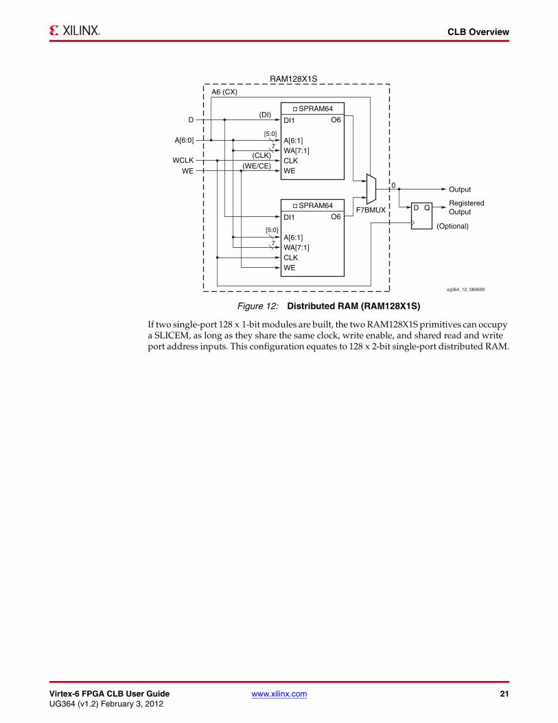
If two single-port 128 x 1-bit modules are built, the two RAM128X1S primitives can occupy a SLICEM, as long as they share the same clock, write enable, and shared read and write port address inputs. This configuration equates to 128 x 2-bit single-port distributed RAM.
X-Ref Target - Figure 12
Figure 12: Distributed RAM (RAM128X1S)
ug364_12_080609
DI1(DI)
A6 (CX)
D
A[6:0]
WCLK
WE
(CLK)
(WE/CE)
[5:0]
[5:0]
7
SPRAM64
RAM128X1S
A[6:1]WA[7:1]CLKWE
O6
DI1
7
SPRAM64
A[6:1]WA[7:1]CLKWE
O6
RegisteredOutput
Output
F7BMUX
(Optional)
D Q
0
22 www.xilinx.com Virtex-6 FPGA CLB User GuideUG364 (v1.2) February 3, 2012
CLB Overview
X-Ref Target - Figure 13
Figure 13: Distributed RAM (RAM128X1D)
ug364_13_080609
DI1DDI
AX
A[6:0]
WCLK
DPRA[6:0]
WE
(CLK)
(WE)
7
DPRAM64
RAM128X1D
A[6:1]WA[7:1]CLKWE
O6
DI1
6
7
DPRAM64
A[6:1]WA[7:1]CLKWE
O6
RegisteredOutputF7BMUX
(Optional)
D Q
SPO
DI1
6
7
DPRAM64
A[6:1]WA[7:1]CLKWE
O6
DI1
6
7
DPRAM64
A[6:1]WA[7:1]CLKWE
O6
RegisteredOutputF7AMUX
(Optional)
D Q
DPO
A6 (CX)
6
Virtex-6 FPGA CLB User Guide www.xilinx.com 23UG364 (v1.2) February 3, 2012
CLB Overview
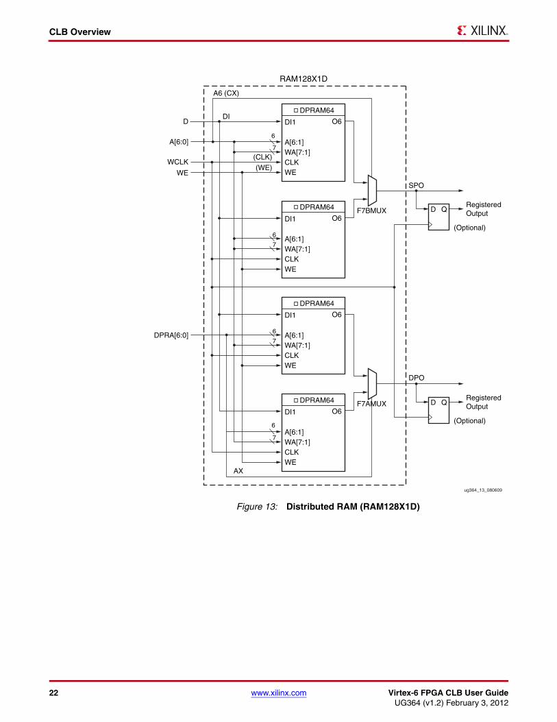
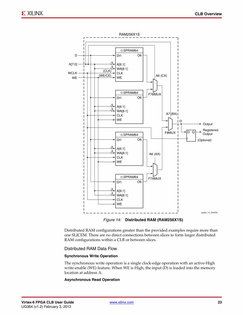
Distributed RAM configurations greater than the provided examples require more than one SLICEM. There are no direct connections between slices to form larger distributed RAM configurations within a CLB or between slices.
Distributed RAM Data Flow
Synchronous Write Operation
The synchronous write operation is a single clock-edge operation with an active-High write-enable (WE) feature. When WE is High, the input (D) is loaded into the memory location at address A.
Asynchronous Read Operation
X-Ref Target - Figure 14
Figure 14: Distributed RAM (RAM256X1S)
ug364_14_040209
DI1D
A[7:0]
WCLK
WE
(CLK)
(WE/CE)
6
8
SPRAM64
RAM256X1S
A[6:1]WA[8:1]CLKWE
O6
DI1
6
8
SPRAM64
A[6:1]WA[8:1]CLKWE
O6F7BMUX
F8MUXRegisteredOutput
Output
(Optional)
D Q
O
DI1
6
8
SPRAM64
A[6:1]WA[8:1]CLKWE
O6
DI1
6
8
SPRAM64
A[6:1]WA[8:1]CLKWE
O6F7AMUX
A6 (CX)
A6 (AX)
A7 (BX)

24 www.xilinx.com Virtex-6 FPGA CLB User GuideUG364 (v1.2) February 3, 2012
CLB Overview
The output is determined by the address A (for single-port mode output/SPO output of dual-port mode), or address DPRA (DPO output of dual-port mode). Each time a new address is applied to the address pins, the data value in the memory location of that address is available on the output after the time delay to access the LUT. This operation is asynchronous and independent of the clock signal.
Distributed RAM Summary
• Single-port and dual-port modes are available in SLICEMs.
• A write operation requires one clock edge.
• Read operations are asynchronous (Q output).
• The data input has a setup-to-clock timing specification.
Read Only Memory (ROM)
Each function generator in SLICEMs and SLICELs can implement a 64 x 1-bit ROM. Three configurations are available: ROM64x1, ROM128x1, and ROM256x1. ROM contents are loaded at each device configuration. Table 5 shows the number of LUTs occupied by each ROM configuration.
Shift Registers (Available in SLICEM only)
A SLICEM function generator can also be configured as a 32-bit shift register without using the flip-flops available in a slice. Used in this way, each LUT can delay serial data anywhere from one to 32 clock cycles. The shiftin D (DI1 LUT pin) and shiftout Q31 (MC31 LUT pin) lines cascade LUTs to form larger shift registers. The four LUTs in a SLICEM are thus cascaded to produce delays up to 128 clock cycles. It is also possible to combine shift registers across more than one SLICEM. Note that there are no direct connections between slices to form longer shift registers, nor is the MC31 output at LUT B/C/D available. The resulting programmable delays can be used to balance the timing of data pipelines.
Applications requiring delay or latency compensation use these shift registers to develop efficient designs. Shift registers are also useful in synchronous FIFO and content addressable memory (CAM) designs.
The write operation is synchronous with a clock input (CLK) and an optional clock enable (CE). A dynamic read access is performed through the 5-bit address bus, A[4:0]. The LSB of the LUT is unused and the software automatically ties it to a logic High. The configurable shift registers cannot be set or reset. The read is asynchronous; however, a storage element or flip-flop is available to implement a synchronous read. In this case, the clock-to-out of the flip-flop determines the overall delay and improves performance. However, one additional cycle of clock latency is added. Any of the 32 bits can be read out asynchronously (at the O6 LUT outputs) by varying the 5-bit address. This capability is useful in creating smaller shift registers (less than 32 bits). For example, when building a 13-bit shift register, simply set the address to the 13th bit. Figure 15 is a logic block diagram of a 32-bit shift register.
Table 5: ROM Configuration
ROM Number of LUTs
64 x 1 1
128 x 1 2
256 x 1 4

Virtex-6 FPGA CLB User Guide www.xilinx.com 25UG364 (v1.2) February 3, 2012
CLB Overview
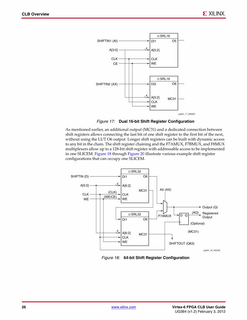
Figure 16 illustrates an example shift register configuration occupying one function generator.
Figure 17 shows two 16-bit shift registers. The example shown can be implemented in a single LUT.
X-Ref Target - Figure 15
Figure 15: 32-bit Shift Register Configuration
X-Ref Target - Figure 16
Figure 16: Representation of a Shift Register
ug364_15_080609
Output (Q)
RegisteredOutput
(Optional)
(AQ)
DI1
D Q
(AI)
SHIFTIN (MC31 of Previous LUT)
SHIFTIN (D)
A[4:0]
CLKCE
(A[6:2])
(CLK)
(WE/CE)
SRL32
SRLC32E
A[6:2]
CLKCE
O6
MC31SHIFTOUT (Q31)
5
ug364_16_040209
SHIFTIN (D)
SHIFTOUT(Q31)WE
CLK
Address (A[4:0])
32-bit Shift Register
MUX
Q
5
26 www.xilinx.com Virtex-6 FPGA CLB User GuideUG364 (v1.2) February 3, 2012
CLB Overview
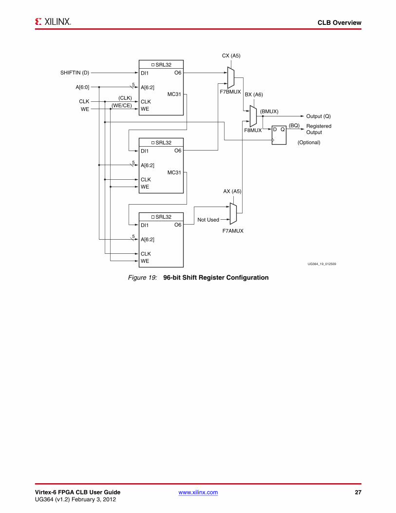
As mentioned earlier, an additional output (MC31) and a dedicated connection between shift registers allows connecting the last bit of one shift register to the first bit of the next, without using the LUT O6 output. Longer shift registers can be built with dynamic access to any bit in the chain. The shift register chaining and the F7AMUX, F7BMUX, and F8MUX multiplexers allow up to a 128-bit shift register with addressable access to be implemented in one SLICEM. Figure 18 through Figure 20 illustrate various example shift register configurations that can occupy one SLICEM.
X-Ref Target - Figure 17
Figure 17: Dual 16-bit Shift Register Configuration
X-Ref Target - Figure 18
Figure 18: 64-bit Shift Register Configuration
ug364_17_080609
DI1SHIFTIN1 (AI)
SHIFTIN2 (AX)
A[3:0]
CLK
CE
4
SRL16
A[5:2]
CLKWE
O5
MC31
DI2
4
SRL16
A[5:2]CLKWE
O6
ug364_18_040209
DI1SHIFTIN (D)
A[5:0]
CLK
WE
(CLK)
(WE/CE)
5
SRL32
A[6:2]
CLKWE
O6
MC31
MC31
DI1
5
SRL32
A[6:2]CLKWE
O6
RegisteredOutput
Output (Q)
F7AMUX
(Optional)
D Q
A5 (AX)
(AQ)
SHIFTOUT (Q63)
(MC31)
Virtex-6 FPGA CLB User Guide www.xilinx.com 27UG364 (v1.2) February 3, 2012
CLB Overview
X-Ref Target - Figure 19
Figure 19: 96-bit Shift Register Configuration
UG364_19_012509
DI1SHIFTIN (D)
A[6:0]
CLK
WE
AX (A5)
(CLK)
(WE/CE)
5
SRL32
A[6:2]
CLKWE
O6
MC31
MC31
DI1
5
SRL32
A[6:2]
CLKWE
O6
F7BMUX
Not Used
F8MUXRegisteredOutput
Output (Q)
(Optional)
D Q(BQ)
(BMUX)
DI1
5
SRL32
A[6:2]
CLKWE
O6F7AMUX
CX (A5)
BX (A6)

28 www.xilinx.com Virtex-6 FPGA CLB User GuideUG364 (v1.2) February 3, 2012
CLB Overview
It is possible to create shift registers longer than 128 bits across more than one SLICEM. However, there are no direct connections between slices to form these shift registers.
Shift Register Data Flow
Shift Operation
The shift operation is a single clock-edge operation, with an active-High clock enable feature. When enable is High, the input (D) is loaded into the first bit of the shift register. Each bit is also shifted to the next highest bit position. In a cascadable shift register configuration, the last bit is shifted out on the M31 output.
The bit selected by the 5-bit address port (A[4:0]) appears on the Q output.
Dynamic Read Operation
The Q output is determined by the 5-bit address. Each time a new address is applied to the 5-input address pins, the new bit position value is available on the Q output after the time
X-Ref Target - Figure 20
Figure 20: 128-bit Shift Register Configuration
ug364_20_040209
DI1SHIFTIN (D)
A[6:0]
CLK
WE
(CLK)
(WE/CE)
5
SRL32
A[6:2]
CLKWE
O6
MC31
MC31
MC31
MC31
DI1
SRL32
A[6:2]
CLKWE
O6F7BMUX
F8MUX
CX (A5)
BX (A6)
RegisteredOutput
Output (Q)
(Optional)
D Q
(BMUX)
SHIFTOUT (Q127)
(MC31)
(BQ)
DI1
SRL32
A[6:2]
CLKWE
O6
DI1
SRL32
A[6:2]
CLKWE
O6F7AMUX
AX (A5)

Virtex-6 FPGA CLB User Guide www.xilinx.com 29UG364 (v1.2) February 3, 2012
CLB Overview
delay to access the LUT. This operation is asynchronous and independent of the clock and clock-enable signals.
Static Read Operation
If the 5-bit address is fixed, the Q output always uses the same bit position. This mode implements any shift-register length from 1 to 32 bits in one LUT. The shift register length is (N+1), where N is the input address (0 – 31).
The Q output changes synchronously with each shift operation. The previous bit is shifted to the next position and appears on the Q output.
Shift Register Summary
• A shift operation requires one clock edge.
• Dynamic-length read operations are asynchronous (Q output).
• Static-length read operations are synchronous (Q output).
• The data input has a setup-to-clock timing specification.
• In a cascadable configuration, the Q31 output always contains the last bit value.
• The Q31 output changes synchronously after each shift operation.
Multiplexers
Function generators and associated multiplexers in Virtex-6 FPGAs can implement the following:
• 4:1 multiplexers using one LUT
• 8:1 multiplexers using two LUTs
• 16:1 multiplexers using four LUTs
These wide input multiplexers are implemented in one level or logic (or LUT) using the dedicated F7AMUX, F7BMUX, and F8MUX multiplexers. These multiplexers allow LUT combinations of up to four LUTs in a slice.
Designing Large Multiplexers
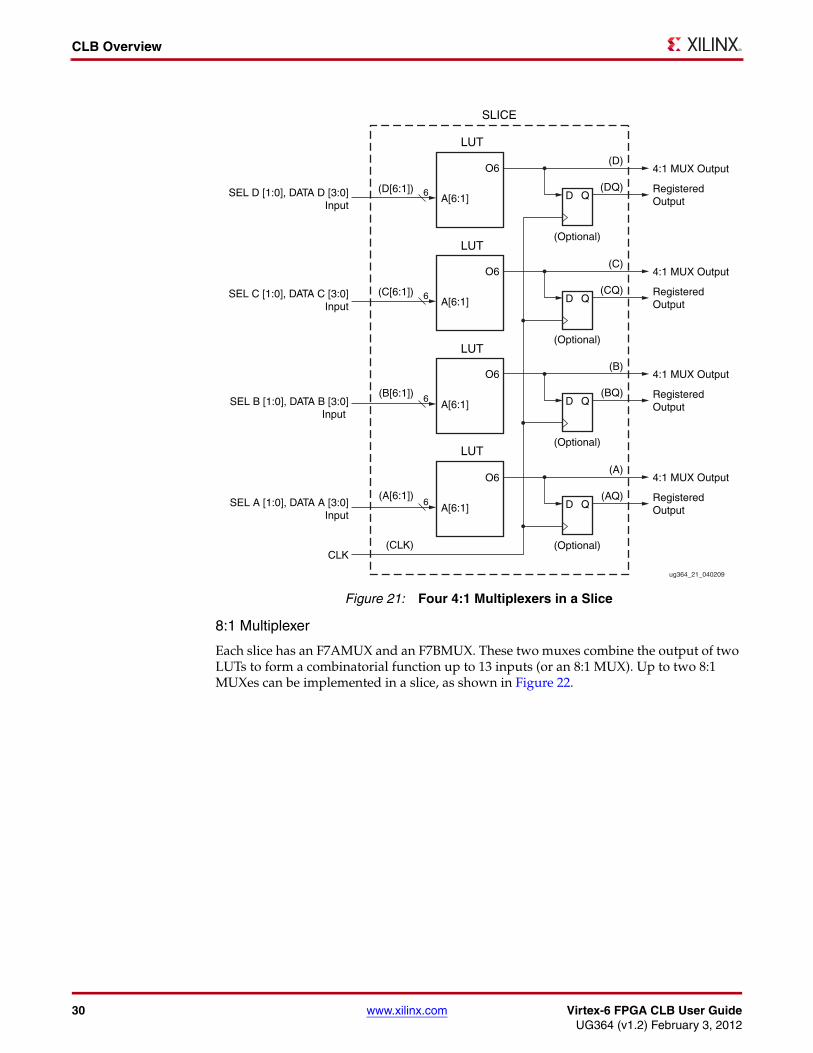
4:1 Multiplexer
Each LUT can be configured into a 4:1 MUX. The 4:1 MUX can be implemented with a flip-flop in the same slice. Up to four 4:1 MUXes can be implemented in a slice, as shown in Figure 21.
30 www.xilinx.com Virtex-6 FPGA CLB User GuideUG364 (v1.2) February 3, 2012
CLB Overview
8:1 Multiplexer
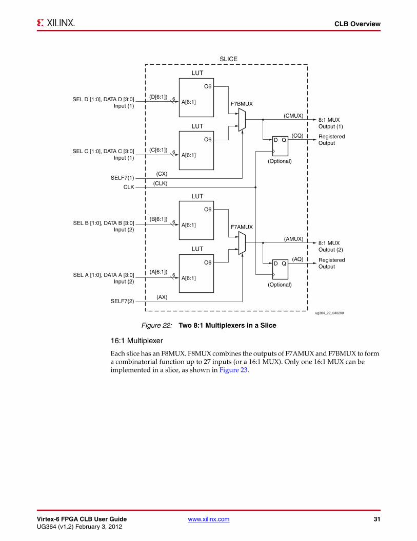
Each slice has an F7AMUX and an F7BMUX. These two muxes combine the output of two LUTs to form a combinatorial function up to 13 inputs (or an 8:1 MUX). Up to two 8:1 MUXes can be implemented in a slice, as shown in Figure 22.
X-Ref Target - Figure 21
Figure 21: Four 4:1 Multiplexers in a Slice
ug364_21_040209
(D[6:1])
(C[6:1])
(B[6:1])
(A[6:1])
(CLK)CLK
6
SLICE
LUT
LUT
LUT
LUT
A[6:1]
O6
6A[6:1]
O6
RegisteredOutput
4:1 MUX Output
(Optional)
D Q
(D)
(DQ)
RegisteredOutput
4:1 MUX Output
(Optional)
D Q
(C)
(CQ)
RegisteredOutput
4:1 MUX Output
(Optional)
D Q
(B)
(BQ)
RegisteredOutput
4:1 MUX Output
(Optional)
D Q
(A)
(AQ)
6A[6:1]
O6
6A[6:1]
O6
SEL D [1:0], DATA D [3:0]Input
SEL C [1:0], DATA C [3:0]Input
SEL B [1:0], DATA B [3:0]Input
SEL A [1:0], DATA A [3:0]Input
Virtex-6 FPGA CLB User Guide www.xilinx.com 31UG364 (v1.2) February 3, 2012
CLB Overview
16:1 Multiplexer
Each slice has an F8MUX. F8MUX combines the outputs of F7AMUX and F7BMUX to form a combinatorial function up to 27 inputs (or a 16:1 MUX). Only one 16:1 MUX can be implemented in a slice, as shown in Figure 23.
X-Ref Target - Figure 22
Figure 22: Two 8:1 Multiplexers in a Slice
ug364_22_040209
(D[6:1])
(C[6:1])
(CX)
(B[6:1])
(A[6:1])
(AX)
SELF7(1)(CLK)
CLK
SELF7(2)
SEL D [1:0], DATA D [3:0]Input (1)
SEL C [1:0], DATA C [3:0]Input (1)
SEL B [1:0], DATA B [3:0]Input (2)
SEL A [1:0], DATA A [3:0]Input (2)
6
SLICE
LUT
LUT
LUT
LUT
A[6:1]
O6
6A[6:1]
O6 RegisteredOutput
8:1 MUXOutput (1)
(Optional)
D Q
(CMUX)
(CQ)
RegisteredOutput
8:1 MUXOutput (2)
(Optional)
D Q
(AMUX)
(AQ)
6A[6:1]
O6
6A[6:1]
O6
F7BMUX
F7AMUX

32 www.xilinx.com Virtex-6 FPGA CLB User GuideUG364 (v1.2) February 3, 2012
CLB Overview
It is possible to create multiplexers wider than 16:1 across more than one SLICEM. However, there are no direct connections between slices to form these wide multiplexers.
Fast Lookahead Carry Logic
In addition to function generators, dedicated carry logic is provided to perform fast arithmetic addition and subtraction in a slice. A Virtex-6 FPGA CLB has two separate carry chains, as shown in Figure 1. The carry chains are cascadable to form wider add/subtract logic, as shown in Figure 2.
The carry chain in the Virtex-6 device is running upward and has a height of four bits per slice. For each bit, there is a carry multiplexer (MUXCY) and a dedicated XOR gate for adding/subtracting the operands with a selected carry bits. The dedicated carry path and carry multiplexer (MUXCY) can also be used to cascade function generators for implementing wide logic functions.
Figure 24 illustrates the carry chain with associated logic elements in a slice.
X-Ref Target - Figure 23
Figure 23: 16:1 Multiplexer in a Slice
ug364_23_040209
(D[6:1])
(C[6:1])
(CX)
(B[6:1])
(A[6:1])
(AX)(BX)
(CLK)
SELF7
SELF7
SELF8
CLK
6
SLICE
LUT
LUT
LUT
LUT
A[6:1]
O6
6A[6:1]
O6
RegisteredOutput
16:1 MUXOutput
(Optional)
D Q
(BMUX)
(B)
6A[6:1]
O6
6A[6:1]
O6
F7BMUX
F8MUX
F7AMUX
SEL D [1:0], DATA D [3:0]Input
SEL C [1:0], DATA C [3:0]Input
SEL B [1:0], DATA B [3:0]Input
SEL A [1:0], DATA A [3:0]Input

Virtex-6 FPGA CLB User Guide www.xilinx.com 33UG364 (v1.2) February 3, 2012
CLB Overview
The carry chains carry lookahead logic along with the function generators. There are ten independent inputs (S inputs – S0 to S3, DI inputs – DI1 to DI4, CYINIT and CIN) and eight independent outputs (O outputs – O0 to O3, and CO outputs – CO0 to CO3).
The S inputs are used for the “propagate” signals of the carry lookahead logic. The “propagate” signals are sourced from the O6 output of a function generator. The DI inputs are used for the “generate” signals of the carry lookahead logic. The “generate” signals are sourced from either the O5 output of a function generator or the BYPASS input (AX, BX, CX, or DX) of a slice. The former input is used to create a multiplier, while the latter is used to create an adder/accumulator. CYINIT is the CIN of the first bit in a carry chain. The CYINIT value can be 0 (for add), 1 (for subtract), or AX input (for the dynamic first carry bit). The CIN input is used to cascade slices to form a longer carry chain. The O outputs contain the sum of the addition/subtraction. The CO outputs compute the carry out for
X-Ref Target - Figure 24
Figure 24: Fast Carry Logic Path and Associated Elements
ug364_24_040209
O6 From LUTD
DMUX/DQ*
DMUX
DQ
O5 From LUTD
DX
S3MUXCY
DI3
CO3
O3
COUT (To Next Slice)
Carry Chain Block(CARRY4)
(Optional)
D Q
O6 From LUTC
CMUX/CQ*
CMUX
CQ
O5 From LUTC
CX
S2MUXCY
DI2
CO2
CO1
CO0
O2
(Optional)
D Q
O6 From LUTB
BMUX/BQ*
BMUX
BQ
O5 From LUTB
BX
S1MUXCY
DI1
O1
(Optional)
D Q
O6 From LUTA
AMUX/AQ*
AMUX
AQ
O5 From LUTA
AX
S0MUXCY
DI0
CIN
CIN (From Previous Slice)
* Can be used ifunregistered/registeredoutputs are free.
CYINIT
10
O0
(Optional)
D Q
ug364_09_040209
34 www.xilinx.com Virtex-6 FPGA CLB User GuideUG364 (v1.2) February 3, 2012
CLB / Slice Timing Models
each bit. CO3 is connected to COUT output of a slice to form a longer carry chain by cascading multiple slices. The propagation delay for an adder increases linearly with the number of bits in the operand, as more carry chains are cascaded. The carry chain can be implemented with a storage element or a flip-flop in the same slice.
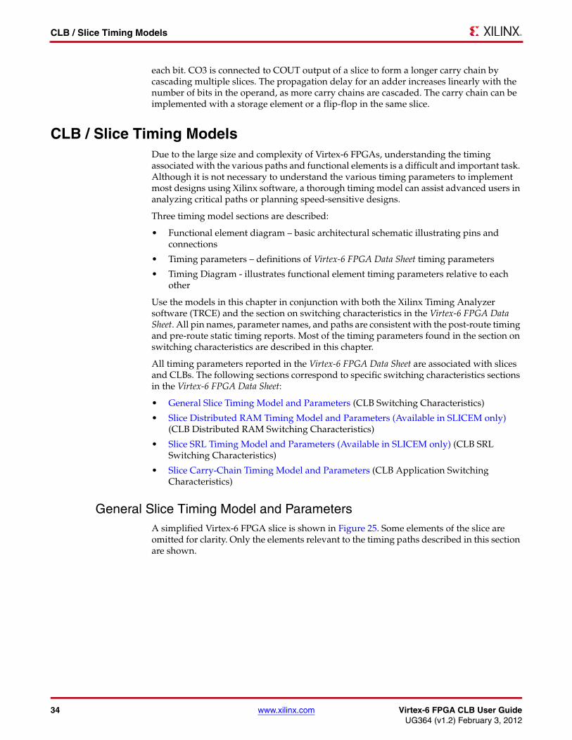
CLB / Slice Timing ModelsDue to the large size and complexity of Virtex-6 FPGAs, understanding the timing associated with the various paths and functional elements is a difficult and important task. Although it is not necessary to understand the various timing parameters to implement most designs using Xilinx software, a thorough timing model can assist advanced users in analyzing critical paths or planning speed-sensitive designs.
Three timing model sections are described:
• Functional element diagram – basic architectural schematic illustrating pins and connections
• Timing parameters – definitions of Virtex-6 FPGA Data Sheet timing parameters
• Timing Diagram - illustrates functional element timing parameters relative to each other
Use the models in this chapter in conjunction with both the Xilinx Timing Analyzer software (TRCE) and the section on switching characteristics in the Virtex-6 FPGA Data Sheet. All pin names, parameter names, and paths are consistent with the post-route timing and pre-route static timing reports. Most of the timing parameters found in the section on switching characteristics are described in this chapter.
All timing parameters reported in the Virtex-6 FPGA Data Sheet are associated with slices and CLBs. The following sections correspond to specific switching characteristics sections in the Virtex-6 FPGA Data Sheet:
• General Slice Timing Model and Parameters (CLB Switching Characteristics)
• Slice Distributed RAM Timing Model and Parameters (Available in SLICEM only) (CLB Distributed RAM Switching Characteristics)
• Slice SRL Timing Model and Parameters (Available in SLICEM only) (CLB SRL Switching Characteristics)
• Slice Carry-Chain Timing Model and Parameters (CLB Application Switching Characteristics)
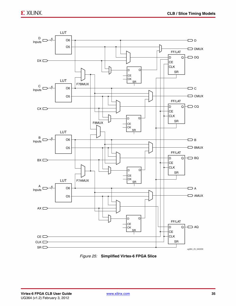
General Slice Timing Model and ParametersA simplified Virtex-6 FPGA slice is shown in Figure 25. Some elements of the slice are omitted for clarity. Only the elements relevant to the timing paths described in this section are shown.
Virtex-6 FPGA CLB User Guide www.xilinx.com 35UG364 (v1.2) February 3, 2012
CLB / Slice Timing Models
X-Ref Target - Figure 25
Figure 25: Simplified Virtex-6 FPGA Slice
ug364_25_040209
LUT
O6
O5
6D
FF/LAT
D
CE
CLK
SR
Q
F7BMUX
F8MUX
DMUX
DQ
D Inputs
LUT
O6
O5
6C
FF/LAT
D
CE
CLK
SR
Q CQ
CMUX
C Inputs
DX
CX
LUT
O6
O5
6B
FF/LAT
D
CE
CLK
SR
Q BQ
BMUX
B Inputs
BX
FF/LAT
D
CE
CLK
SR
Q AQ
F7AMUXLUT
O6
O5
6A
AMUX
A Inputs
AX
CE
CLK
SR
D
CE
Q
CKSR
D
CE
Q
CKSR
D
CE
Q
CKSR
D
CE
Q
CKSR
36 www.xilinx.com Virtex-6 FPGA CLB User GuideUG364 (v1.2) February 3, 2012
CLB / Slice Timing Models
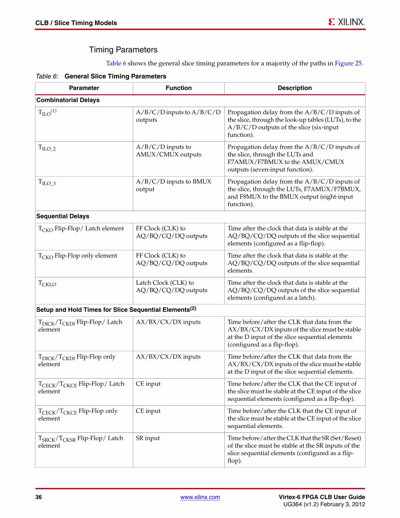
Timing Parameters
Table 6 shows the general slice timing parameters for a majority of the paths in Figure 25.
Table 6: General Slice Timing Parameters
Parameter Function Description
Combinatorial Delays
TILO(1) A/B/C/D inputs to A/B/C/D
outputsPropagation delay from the A/B/C/D inputs of the slice, through the look-up tables (LUTs), to the A/B/C/D outputs of the slice (six-input function).
TILO_2 A/B/C/D inputs to AMUX/CMUX outputs
Propagation delay from the A/B/C/D inputs of the slice, through the LUTs and F7AMUX/F7BMUX to the AMUX/CMUX outputs (seven-input function).
TILO_3 A/B/C/D inputs to BMUX output
Propagation delay from the A/B/C/D inputs of the slice, through the LUTs, F7AMUX/F7BMUX, and F8MUX to the BMUX output (eight-input function).
Sequential Delays
TCKO Flip-Flop/ Latch element FF Clock (CLK) to AQ/BQ/CQ/DQ outputs
Time after the clock that data is stable at the AQ/BQ/CQ/DQ outputs of the slice sequential elements (configured as a flip-flop).
TCKO Flip-Flop only element FF Clock (CLK) to AQ/BQ/CQ/DQ outputs
Time after the clock that data is stable at the AQ/BQ/CQ/DQ outputs of the slice sequential elements.
TCKLO Latch Clock (CLK) to AQ/BQ/CQ/DQ outputs
Time after the clock that data is stable at the AQ/BQ/CQ/DQ outputs of the slice sequential elements (configured as a latch).
Setup and Hold Times for Slice Sequential Elements(2)
TDICK/TCKDI Flip-Flop/ Latch element
AX/BX/CX/DX inputs Time before/after the CLK that data from the AX/BX/CX/DX inputs of the slice must be stable at the D input of the slice sequential elements (configured as a flip-flop).
TDICK/TCKDI Flip-Flop only element
AX/BX/CX/DX inputs Time before/after the CLK that data from the AX/BX/CX/DX inputs of the slice must be stable at the D input of the slice sequential elements.
TCECK/TCKCE Flip-Flop/ Latch element
CE input Time before/after the CLK that the CE input of the slice must be stable at the CE input of the slice sequential elements (configured as a flip-flop).
TCECK/TCKCE Flip-Flop only element
CE input Time before/after the CLK that the CE input of the slice must be stable at the CE input of the slice sequential elements.
TSRCK/TCKSR Flip-Flop/ Latch element
SR input Time before/after the CLK that the SR (Set/Reset) of the slice must be stable at the SR inputs of the slice sequential elements (configured as a flip-flop).
Virtex-6 FPGA CLB User Guide www.xilinx.com 37UG364 (v1.2) February 3, 2012
CLB / Slice Timing Models
Timing Characteristics
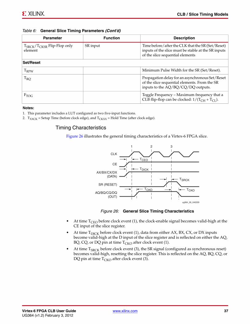
Figure 26 illustrates the general timing characteristics of a Virtex-6 FPGA slice.
• At time TCEO before clock event (1), the clock-enable signal becomes valid-high at the CE input of the slice register.
• At time TDICK before clock event (1), data from either AX, BX, CX, or DX inputs become valid-high at the D input of the slice register and is reflected on either the AQ, BQ, CQ, or DQ pin at time TCKO after clock event (1).
• At time TSRCK before clock event (3), the SR signal (configured as synchronous reset) becomes valid-high, resetting the slice register. This is reflected on the AQ, BQ, CQ, or DQ pin at time TCKO after clock event (3).
TSRCK/TCKSR Flip-Flop only element
SR input Time before/after the CLK that the SR (Set/Reset) inputs of the slice must be stable at the SR inputs of the slice sequential elements
Set/Reset
TRPW Minimum Pulse Width for the SR (Set/Reset).
TRQ Propagation delay for an asynchronous Set/Reset of the slice sequential elements. From the SR inputs to the AQ/BQ/CQ/DQ outputs.
FTOG Toggle Frequency – Maximum frequency that a CLB flip-flop can be clocked: 1/(TCH + TCL).
Notes: 1. This parameter includes a LUT configured as two five-input functions.2. TXXCK = Setup Time (before clock edge), and TCKXX = Hold Time (after clock edge).
Table 6: General Slice Timing Parameters (Cont’d)
Parameter Function Description
X-Ref Target - Figure 26
Figure 26: General Slice Timing Characteristics
ug364_26_040209
TCEO
1 2 3
CLK
CE
AX/BX/CX/DX(DATA)
SR (RESET)
AQ/BQ/CQ/DQ(OUT)
TDICK
TCKO
TSRCK
TCKO

38 www.xilinx.com Virtex-6 FPGA CLB User GuideUG364 (v1.2) February 3, 2012
CLB / Slice Timing Models
Slice Distributed RAM Timing Model and Parameters (Available in SLICEM only)
Figure 27 illustrates the details of distributed RAM implemented in a Virtex-6 FPGA slice. Some elements of the slice are omitted for clarity. Only the elements relevant to the timing paths described in this section are shown.X-Ref Target - Figure 27
Figure 27: Simplified Virtex-6 FPGA SLICEM Distributed RAM
ug364_27_080609
6D
DIDX
D input
CICX
C input
BIBX
B input
AIAX
A input
CLKWE
WA[6:0]
RAM
CLKWE
DI1DI2A[6:0]
O6
DMUXO5
6C
WA[6:0]
RAM
CLKWE
DI1DI2A[6:0]
O6
CMUXO5
6B
WA[6:0]
RAM
CLKWE
DI1DI2A[6:0]
O6
BMUXO5
6A
WA[6:0]
RAM
CLKWE
DI1DI2A[6:0]
O6
AMUXO5
Virtex-6 FPGA CLB User Guide www.xilinx.com 39UG364 (v1.2) February 3, 2012
CLB / Slice Timing Models
Distributed RAM Timing Parameters
Table 7 shows the timing parameters for the distributed RAM in SLICEM for a majority of the paths in Figure 27.
Table 7: Distributed RAM Timing Parameters
Parameter Function Description
Sequential Delays for a Slice LUT Configured as RAM (Distributed RAM)
TSHCKO(1) CLK to A/B/C/D outputs Time after the CLK of a write operation that the
data written to the distributed RAM is stable on the A/B/C/D output of the slice.
Setup and Hold Times for a Slice LUT Configured as RAM (Distributed RAM)(2)
TDS/TDH(3) AI/BI/CI/DI configured as
data input (DI1)Time before/after the clock that data must be stable at the AI/BI/CI/DI input of the slice.
TACK/TCKA A/B/C/D address inputs Time before/after the clock that address signals must be stable at the A/B/C/D inputs of the slice LUT (configured as RAM).
TWS/TWH WE input Time before/after the clock that the write enable signal must be stable at the WE input of the slice LUT (configured as RAM).
Clock CLK
TWPH Minimum Pulse Width, High
TWPL Minimum Pulse Width, Low
TWC Minimum clock period to meet address write cycle time.
Notes: 1. This parameters includes a LUT configured as a two-bit distributed RAM.2. TXXCK = Setup Time (before clock edge), and TCKXX = Hold Time (after clock edge).3. Parameter includes AX/BX/CX/DX configured as a data input (DI2).
40 www.xilinx.com Virtex-6 FPGA CLB User GuideUG364 (v1.2) February 3, 2012
CLB / Slice Timing Models
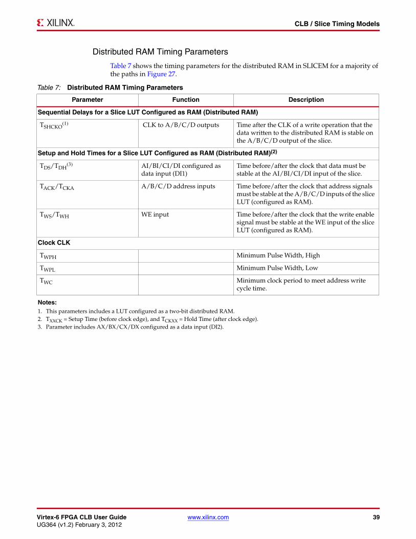
Distributed RAM Timing Characteristics
The timing characteristics of a 16-bit distributed RAM implemented in a Virtex-6 FPGA slice (LUT configured as RAM) are shown in Figure 28.
Clock Event 1: Write Operation
During a Write operation, the contents of the memory at the address on the ADDR inputs are changed. The data written to this memory location is reflected on the A/B/C/D outputs synchronously.
• At time TWS before clock event 1, the write-enable signal (WE) becomes valid-high, enabling the RAM for a Write operation.
• At time TAS before clock event 1, the address (2) becomes valid at the A/B/C/D inputs of the RAM.
• At time TDS before clock event 1, the DATA becomes valid (1) at the DI input of the RAM and is reflected on the A/B/C/D output at time TSHCKO after clock event 1.
This is also applicable to the AMUX, BMUX, CMUX, DMUX, and COUT outputs at time TSHCKO and TWOSCO after clock event 1.
Clock Event 2: Read Operation
All Read operations are asynchronous in distributed RAM. As long as WE is Low, the address bus can be asserted at any time. The contents of the RAM on the address bus are reflected on the A/B/C/D outputs after a delay of length TILO (propagation delay through a LUT). The address (F) is asserted after clock event 2, and the contents of the RAM at address (F) are reflected at the output after a delay of length TILO.
X-Ref Target - Figure 28
Figure 28: Slice Distributed RAM Timing Characteristics
ug364_28_080609
TWPL
TWPH
TWC
1 2 3 4 5 6 7
CLK
WE
DATA_OUTA/B/C/D
Output
A/B/C/D(ADDR)
AI/BI/CI/DI(DI)
TAS
2
1
1 0 01MEM(F)
WRITE WRITE WRITE WRITEREAD READ
MEM(E)
X X0 01
F 3 4 5 E
TDS
TWS TILO TILO
TSHCKO
Virtex-6 FPGA CLB User Guide www.xilinx.com 41UG364 (v1.2) February 3, 2012
CLB / Slice Timing Models
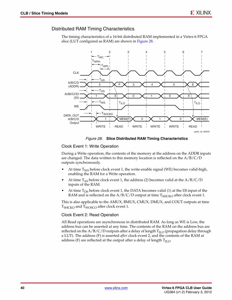
Slice SRL Timing Model and Parameters (Available in SLICEM only)Figure 29 illustrates shift register implementation in a Virtex-6 FPGA slice. Some elements of the slice have been omitted for clarity. Only the elements relevant to the timing paths described in this section are shown.X-Ref Target - Figure 29
Figure 29: Simplified Virtex-6 FPGA Slice SRL
ug364_29_080609
6
DDI
CI
BI
AI
D address
SRL
CLK WE
DI1
A
O6
MC31
WCLK
6
C
C address
SRL
CLK WE
DI1
A
O6
MC31
6
B
B address
SRL
CLK WE
DI1
A
O6
MC31
6
A
A address
SRL
CLK WE
DI1
A
O6
DMUXMC31

42 www.xilinx.com Virtex-6 FPGA CLB User GuideUG364 (v1.2) February 3, 2012
CLB / Slice Timing Models
Slice SRL Timing Parameters
Table 8 shows the SLICEM SRL timing parameters for a majority of the paths in Figure 29.
Slice SRL Timing Characteristics
Figure 30 illustrates the timing characteristics of a 16-bit shift register implemented in a Virtex-6 FPGA slice (a LUT configured as an SRL).
Table 8: Slice SRL Timing Parameters
Parameter Function Description
Sequential Delays for a Slice LUT Configured as an SRL
TREG(1) CLK to A/B/C/D outputs Time after the CLK of a write operation that the
data written to the SRL is stable on the A/B/C/D outputs of the slice.
TREG_MUX(1) CLK to AMUX - DMUX output Time after the CLK of a write operation that the
data written to the SRL is stable on the DMUX output of the slice.
TREG_M31 CLK to DMUX output via MC31 output
Time after the CLK of a write operation that the data written to the SRL is stable on the DMUX output via MC31 output.
Setup and Hold Times for a Slice LUT Configured SRL(2)
TWS/TWH CE input (WE) Time before/after the clock that the write enable signal must be stable at the WE input of the slice LUT (configured as an SRL).
TDS/TDH(3) AI/BI/CI/DI configured as
data input (DI)Time before the clock that the data must be stable at the AI/BI/CI/DI input of the slice (configured as an SRL).
Notes: 1. This parameter includes a LUT configured as a two-bit shift register.2. TXXCK = Setup Time (before clock edge), and TCKXX = Hold Time (after clock edge).3. Parameter includes AX/BX/CX/DX configured as a data input (DI2) or two bits with a common shift.
X-Ref Target - Figure 30
Figure 30: Slice SRL Timing Characteristics
ug364_30_040209
1 2 3 4 5 6 32
CLK
Write Enable(WE)
Shift_In (DI)
Address(A/B/C/D)
Data Out(A/B/C/D)
MSB(MC31/DMUX)
TDS
TILO TILO
0 1 1 0 1 0
20
X
X X X X X X X 0
0 1 1 1 1 10 0
TREG
TREG
TWS
1
Virtex-6 FPGA CLB User Guide www.xilinx.com 43UG364 (v1.2) February 3, 2012
CLB / Slice Timing Models
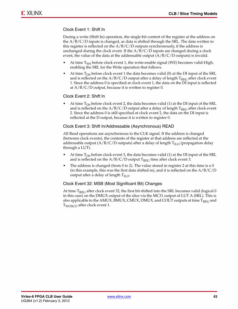
Clock Event 1: Shift In
During a write (Shift In) operation, the single-bit content of the register at the address on the A/B/C/D inputs is changed, as data is shifted through the SRL. The data written to this register is reflected on the A/B/C/D outputs synchronously, if the address is unchanged during the clock event. If the A/B/C/D inputs are changed during a clock event, the value of the data at the addressable output (A/B/C/D outputs) is invalid.
• At time TWS before clock event 1, the write-enable signal (WE) becomes valid-High, enabling the SRL for the Write operation that follows.
• At time TDS before clock event 1 the data becomes valid (0) at the DI input of the SRL and is reflected on the A/B/C/D output after a delay of length TREG after clock event 1. Since the address 0 is specified at clock event 1, the data on the DI input is reflected at A/B/C/D output, because it is written to register 0.
Clock Event 2: Shift In
• At time TDS before clock event 2, the data becomes valid (1) at the DI input of the SRL and is reflected on the A/B/C/D output after a delay of length TREG after clock event 2. Since the address 0 is still specified at clock event 2, the data on the DI input is reflected at the D output, because it is written to register 0.
Clock Event 3: Shift In/Addressable (Asynchronous) READ
All Read operations are asynchronous to the CLK signal. If the address is changed (between clock events), the contents of the register at that address are reflected at the addressable output (A/B/C/D outputs) after a delay of length TILO (propagation delay through a LUT).
• At time TDS before clock event 3, the data becomes valid (1) at the DI input of the SRL and is reflected on the A/B/C/D output TREG time after clock event 3.
• The address is changed (from 0 to 2). The value stored in register 2 at this time is a 0 (in this example, this was the first data shifted in), and it is reflected on the A/B/C/D output after a delay of length TILO.
Clock Event 32: MSB (Most Significant Bit) Changes
At time TREG after clock event 32, the first bit shifted into the SRL becomes valid (logical 0 in this case) on the DMUX output of the slice via the MC31 output of LUT A (SRL). This is also applicable to the AMUX, BMUX, CMUX, DMUX, and COUT outputs at time TREG and TWOSCO after clock event 1.

44 www.xilinx.com Virtex-6 FPGA CLB User GuideUG364 (v1.2) February 3, 2012
CLB / Slice Timing Models
Slice Carry-Chain Timing Model and ParametersFigure 24, page 33 illustrates a carry chain in a Virtex-6 FPGA slice. Some elements of the slice have been omitted for clarity. Only the elements relevant to the timing paths described in this section are shown.
Slice Carry-Chain Timing Parameters
Table 9 shows the slice carry-chain timing parameters for a majority of the paths in Figure 24, page 33.
Slice Carry-Chain Timing Characteristics
Figure 31 illustrates the timing characteristics of a slice carry chain implemented in a Virtex-6 FPGA slice.
Table 9: Slice Carry-Chain Timing Parameters
Parameter Function Description
Sequential Delays for Slice LUT Configured as Carry Chain
TAXCY/TBXCY/TCXCY/TDXCY AX/BX/CX/DX input to COUT output
Propagation delay from the AX/BX/CX/DX inputs of the slice to the COUT output of the slice.
TBYP CIN input to COUT output Propagation delay from the CIN input of the slice to the COUT output of the slice.
TOPCYA/TOPCYB/TOPCYC/TOPCYD A/B/C/D input to COUT output
Propagation delay from the A/B/C/D inputs of the slice to the COUT output of the slice.
TCINA/TCINB/TCINC/TCIND A/B/C/D input to AMUX/BMUX/CMUX/DMUX output
Propagation delay from the A/B/C/D inputs of the slice to AMUX/BMUX/CMUX/DMUX output of the slice using XOR (sum).
Setup and Hold Times for a Slice LUT Configured as a Carry Chain(1)
TCINCK/TCKCIN CIN Data inputs Time before the CLK that data from the CIN input of the slice must be stable at the D input of the slice sequential elements (configured as a flip-flop).
Notes: 1. TXXCK = Setup Time (before clock edge), and TCKXX = Hold Time (after clock edge).
X-Ref Target - Figure 31
Figure 31: Slice Carry-Chain Timing Characteristics
ug364_31_040209
TCINCK
1 2 3
CLK
CIN(DATA)
SR (RESET)
AQ/BQ/CQ/DQ(OUT)
TCKO
TSRCK
TCKO
Virtex-6 FPGA CLB User Guide www.xilinx.com 45UG364 (v1.2) February 3, 2012
CLB Primitives
• At time TCINCK before clock event 1, data from CIN input becomes valid-high at the D input of the slice register. This is reflected on any of the AQ/BQ/CQ/DQ pins at time TCKO after clock event 1.
• At time TSRCK before clock event 3, the SR signal (configured as synchronous reset) becomes valid-high, resetting the slice register. This is reflected on any of the AQ/BQ/CQ/DQ pins at time TCKO after clock event 3.
CLB PrimitivesMore information on the CLB primitives are available in the software libraries guide.
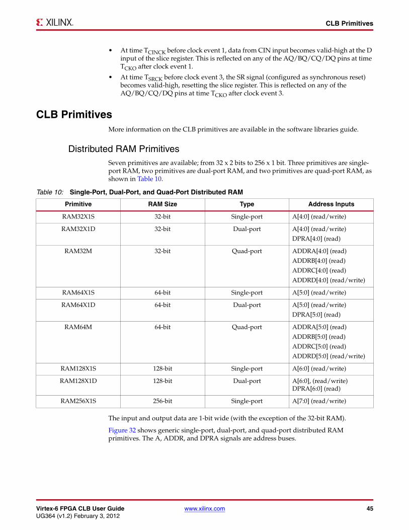
Distributed RAM PrimitivesSeven primitives are available; from 32 x 2 bits to 256 x 1 bit. Three primitives are single-port RAM, two primitives are dual-port RAM, and two primitives are quad-port RAM, as shown in Table 10.
The input and output data are 1-bit wide (with the exception of the 32-bit RAM).
Figure 32 shows generic single-port, dual-port, and quad-port distributed RAM primitives. The A, ADDR, and DPRA signals are address buses.
Table 10: Single-Port, Dual-Port, and Quad-Port Distributed RAM
Primitive RAM Size Type Address Inputs
RAM32X1S 32-bit Single-port A[4:0] (read/write)
RAM32X1D 32-bit Dual-port A[4:0] (read/write)
DPRA[4:0] (read)
RAM32M 32-bit Quad-port ADDRA[4:0] (read)
ADDRB[4:0] (read)
ADDRC[4:0] (read)
ADDRD[4:0] (read/write)
RAM64X1S 64-bit Single-port A[5:0] (read/write)
RAM64X1D 64-bit Dual-port A[5:0] (read/write)
DPRA[5:0] (read)
RAM64M 64-bit Quad-port ADDRA[5:0] (read)
ADDRB[5:0] (read)
ADDRC[5:0] (read)
ADDRD[5:0] (read/write)
RAM128X1S 128-bit Single-port A[6:0] (read/write)
RAM128X1D 128-bit Dual-port A[6:0], (read/write) DPRA[6:0] (read)
RAM256X1S 256-bit Single-port A[7:0] (read/write)

46 www.xilinx.com Virtex-6 FPGA CLB User GuideUG364 (v1.2) February 3, 2012
CLB Primitives
Instantiating several distributed RAM primitives can be used to implement wide memory blocks.
Port Signals
Each distributed RAM port operates independently of the other while reading the same set of memory cells.
Clock – WCLK
The clock is used for the synchronous write. The data and the address input pins have setup times referenced to the WCLK pin.
Enable – WE/WED
The enable pin affects the write functionality of the port. An inactive write enable prevents any writing to memory cells. An active write enable causes the clock edge to write the data input signal to the memory location pointed to by the address inputs.
Address – A[#:0], DPRA[#:0], and ADDRA[#:0] – ADDRD[#:0]
The address inputs A[#:0] (for single-port and dual-port), DPRA[#:0] (for dual-port), and ADDRA[#:0] – ADDRD[#:0] (for quad-port) select the memory cells for read or write. The width of the port determines the required address inputs. Some of the address inputs are not buses in VHDL or Verilog instantiations. Table 10 summarizes the function of each address pins.
Data In – D, DID[#:0]
The data input D (for single-port and dual-port) and DID[#:0] (for quad-port) provide the new data value to be written into the RAM.
Data Out – O, SPO, DPO and DOA[#:0] – DOD[#:0]
The data out O (single-port or SPO), DPO (dual-port), and DOA[#:0] – DOD[#:0] (quad-port) reflects the contents of the memory cells referenced by the address inputs. Following an active write clock edge, the data out (O, SPO, or DOD[#:0]) reflects the newly written data.
X-Ref Target - Figure 32
Figure 32: Single-Port, Dual-Port, and Quad-Port Distributed RAM Primitives
RAM#X1S
ug364_32_040209
DO
WE
WCLK
A[#:0]
SPO DOD[#:0]
RAM#X1D
D
DPO
R/W Port
Read Port
WE
WCLK
A[#:0]
DPRA[#:0]
RAM#M
DI[A:D][#:0]
DOC[#:0]
R/W Port
Read Port
Read Port
Read Port
WE
WCLK
ADDRD[#:0]
ADDRC[#:0]
DOB[#:0]ADDRB[#:0]
DOA[#:0]ADDRA[#:0]

Virtex-6 FPGA CLB User Guide www.xilinx.com 47UG364 (v1.2) February 3, 2012
CLB Primitives
Inverting Clock Pins
The clock pin (CLK) has an individual inversion option. The clock signal can be active at the negative edge of the clock or the positive edge of the clock without requiring other logic resources. The default is at the positive clock edge.
Global Set/Reset – GSR
The global set/reset (GSR) signal does not affect distributed RAM modules.
Shift Registers (SRLs) PrimitiveOne primitive is available for the 32-bit shift register (SRLC32E). Figure 33 shows the 32-bit shift register primitive.
Instantiating several 32-bit shift register with dedicated multiplexers (F7AMUX, F7BMUX, and F8MUX) allows a cascadable shift register chain of up to 128-bit in a slice. Figure 18 through Figure 20 in the Shift Registers (Available in SLICEM only) section of this document illustrate the various implementation of cascadable shift registers greater than 32 bits.
Port Signals
Clock – CLK
Either the rising edge or the falling edge of the clock is used for the synchronous shift operation. The data and clock enable input pins have setup times referenced to the chosen edge of CLK.
Data In – D
The data input provides new data (one bit) to be shifted into the shift register.
Clock Enable - CE
The clock enable pin affects shift functionality. An inactive clock enable pin does not shift data into the shift register and does not write new data. Activating the clock enable allows the data in (D) to be written to the first location and all data to be shifted by one location. When available, new data appears on output pins (Q) and the cascadable output pin (Q31).
Address – A[4:0]
The address input selects the bit (range 0 to 31) to be read. The nth bit is available on the output pin (Q). Address inputs have no effect on the cascadable output pin (Q31). It is always the last bit of the shift register (bit 31).
X-Ref Target - Figure 33
Figure 33: 32-bit Shift Register
SRLC32E
ug364_33_040209
DQ
A[4:0]6
CE
CLK
Q31

48 www.xilinx.com Virtex-6 FPGA CLB User GuideUG364 (v1.2) February 3, 2012
CLB Primitives
Data Out – Q
The data output Q provides the data value (1 bit) selected by the address inputs.
Data Out – Q31 (optional)
The data output Q31 provides the last bit value of the 32-bit shift register. New data becomes available after each shift-in operation.
Inverting Clock Pins
The clock pin (CLK) has an individual inversion option. The clock signal can be active at the negative or positive edge of the clock without requiring other logic resources. The default is positive clock edge.
Global Set/Reset – GSR
The global set/reset (GSR) signal does not affect the shift registers.
Other Shift Register Applications
Synchronous Shift Registers
The shift-register primitive does not use the register available in the same slice. To implement a fully synchronous read and write shift register, output pin Q must be connected to a flip-flop. Both the shift register and the flip-flop share the same clock, as shown in Figure 34.
This configuration provides a better timing solution and simplifies the design. Because the flip-flop must be considered to be the last register in the shift-register chain, the static or dynamic address should point to the desired length minus one. If needed, the cascadable output can also be registered in a flip-flop.
Static-Length Shift Registers
The cascadable 32-bit shift register implements any static length mode shift register without the dedicated multiplexers (F7AMUX, F7BMUX, and F8MUX). Figure 35 illustrates a 72-bit shift register. Only the last SRLC32E primitive needs to have its address inputs tied to 0b00111. Alternatively, shift register length can be limited to 71 bits (address tied to 0b00110) and a flip-flop can be used as the last register. (In an SRLC32E primitive, the shift register length is the address input + 1).
X-Ref Target - Figure 34
Figure 34: Synchronous Shift Register
SynchronousOutputD QD Q
Address
CLK
(Write Enable)CE
SRLC32G FF
Q31
ug364_34_040209

Virtex-6 FPGA CLB User Guide www.xilinx.com 49UG364 (v1.2) February 3, 2012
CLB Primitives
Multiplexer PrimitivesTwo primitives (MUXF7 and MUXF8) are available for access to the dedicated F7AMUX, F7BMUX and F8MUX in each slice. Combined with LUTs, these multiplexer primitives are also used to build larger width multiplexers (from 8:1 to 16:1). The Designing Large Multiplexers section provides more information on building larger multiplexers.
Port Signals
Data In – I0, I1
The data input provides the data to be selected by the select signal (S).
Control In – S
The select input signal determines the data input signal to be connected to the output O. Logic 0 selects the I0 input, while logic 1 selects the I1 input.
Data Out – O
The data output O provides the data value (one bit) selected by the control inputs.
Carry Chain PrimitiveThe CARRY4 primitive represents the fast carry logic for a slice in the Virtex-6 architecture. This primitive works in conjunction with LUTs in order to build adders and multipliers. This primitive is generally inferred by synthesis tools from standard RTL code. The synthesis tool can identify the arithmetic and/or logic functionality that best maps to this
X-Ref Target - Figure 35
Figure 35: Example Static-Length Shift Register
LUT
SRLC32G
D
Q31
LUT
SRLC32G
D
Q31
LUT
SRLC32G
D OUT(72-bit SRL)
A[4:0]
Q31
Q
500111
D
ug364_35_040209
LUT
SRLC32G
D
Q31
LUT
SRLC32G
D
Q31
LUT
SRLC32G
D OUT(72-bit SRL)
A[4:0]
Q31
Q
FF
D Q
500110
D
50 www.xilinx.com Virtex-6 FPGA CLB User GuideUG364 (v1.2) February 3, 2012
CLB Primitives
logic in terms of performance and area. It also automatically uses and connects this function properly. Figure 24, page 33 illustrates the CARRY4 block diagram.
Port Signals
Sum Outputs – O[3:0]
The sum outputs provide the final result of the addition/subtraction.
Carry Outputs – CO[3:0]
The carry outputs provide the carry out for each bit. A longer carry chain can be created if CO[3] is connected to CI input of another CARRY4 primitive.
Data Inputs – DI[3:0]
The data inputs are used as “generate” signals to the carry lookahead logic. The “generate” signals are sourced from LUT outputs.
Select Inputs – S[3:0]
The select inputs are used as “propagate” signals to the carry lookahead logic. The “propagate” signals are sourced from LUT outputs.
Carry Initialize – CYINIT
The carry initialize input is used to select the first bit in a carry chain. The value for this pin is either 0 (for add), 1 (for subtract), or AX input (for the dynamic first carry bit).
Carry In – CI
The carry in input is used to cascade slices to form longer carry chain. To create a longer carry chain, the CO[3] output of another CARRY4 is simply connected to this pin.