Embed Size (px)
Citation preview
7/13/2009 1
Digital Engineering Laboratory
Course Introduction & FPGA
Concepts and Design
ECE 554
Department of Electrical and
Computer Engineering
University of Wisconsin - Madison
2009-7-13 2
Instructors and Course Website
• Nam Sung Kim, [email protected]– Office: 4615 Engineering Hall
– Office hours: Tue,Wed,Thur - 2:00 to 3:00 PM
Additional hours by appointment
• Chunhua Yao, [email protected]– Teaching Assistant for Labs
– Office hours are assigned lab hours – 3:30 to 6:30 Tuesday and Thursday
• The course website and wiki are at:
http://homepages.cae.wisc.edu/~ece554/new_website/
https://cgi.cae.wisc.edu/~ece554/pmwiki/pmwiki.php
7/13/2009 3
Course Objectives
• Deal with problems and solutions associated with many aspects of a large digital design project
• Work effectively as a member of a moderate-sized team
• Use contemporary commercial design tools
• Use programmable user-defined devices (FPGAs) for rapid prototyping
• Learn to live on Pizza and get by on very little sleep at least during the last part of the course.
7/13/2009 4
Prerequisites and Location• ECE 351 – Digital Logic Laboratory
• ECE/CS 552 – Introduction to Computer
Architecture
• ECE 551 - Digital System Design and
Synthesis (strongly recommended)
• Laboratory: 3628 Engineering Hall
• Lecture: 3444 EH
• Lectures and Reviews during Lab Hours:
3444 EH
7/13/2009 5
Access to the lab
• Laboratory: 3628 Engineering Hall
The lab access is password protected and
you will have access to the lab 24/7
• Password
2009-7-13 6
Course Overview Grading
• 15% Miniproject – due 2/5
– Design a Special Purpose Asynchronous
Receiver/Transmitter (team of 2)
• 20% Bench Exam – on 2/26
– Designed to test your understanding of Design
Specifications, Verilog, Debugging, Lab Environment,
etc. (individual)
• 65% Project – demos 5/5, report 5/14
– Design, implement, test, and program a general or
special purpose digital computer that emphasizes
some particular features (team of 4 to 6)
7/13/2009 7
Miniproject
• For the miniproject, you will – Design a Special Purpose Asynchronous
Receiver/Transmitter (SPART) and its testbench in
Verilog/VHDL and use EDK toolset
– Simulate the design to ensure correct performance
– Download the design and associated files and
demonstrate correct functionality
– Preparing a report on your design
– https://cgi.cae.wisc.edu/~ece554/pmwiki/pmwiki.php?
n=Main.MiniProject
7/13/2009 8
Midterm Bench Exam• You will be given a set of specifications for a small
system along with Verilog code for some pre-designed
modules for the system.
• You will be expected to:
– Understand the specifications
– Understand the Verilog code provided
– Write one or more Verilog modules
– Debug one or more Verilog modules
– Simulate one or more modules and the entire system
– Synthesize and implement the design
– Download, test, and demonstrate the design on the
FPGA board
7/13/2009 9
Project• Design, simulate, synthesize, test, download and
demonstrate a non-trivial computer with an original
instruction set architecture (ISA)
• Four key requirements
– It must be an original ISA (somewhat negotiable)
– It must be non-trivial
– It must be tractable - everything takes at least twice as
long as you expect
– It must interface through the serial port with the
terminal emulator on the lab workstations (negotiable)
• Often has significant software component and utilizes
FPGA board interfaces
2009-7-13 10
Project Milestone• Several major milestones
– Project team selection – each team of 5 or 6 (2/3)
– Project proposal presentation (2/12)
– Architecture review presentation (2/19)
– ISA report due (2/24)
– Microarchitecture review presentation (3/24)
– Testing and demo review presentation (4/7)
– Several progress reviews (see syllabus)
– Project demonstrations (5/5)
– Project report due (5/14)
• For details see:
https://cgi.cae.wisc.edu/~ece554/pmwiki/pmwiki.php?n=Main.Milestones
7/13/2009 11
Major Lab Enhancement
• We have done a major enhancement to the
ECE554 lab recently, bear with us for version
updates
– All new computers and monitors
– All new FPGA boards and updated digital design
software
– Overall objectives of the lab will stay the same
– Some additional changes may happen this semester
– We will try to make the transition as smooth as
possible – thanks to Mitch
• Go over the syllabus
7/13/2009 12
FPGA Concepts and Design
• CMOS IC design alternatives
• RAM cell-based FPGA uses
• The Xilinx Virtex Series FPGA technology
• The Xilinx Integrated Software Environment (ISE)
design process
7/13/2009 13
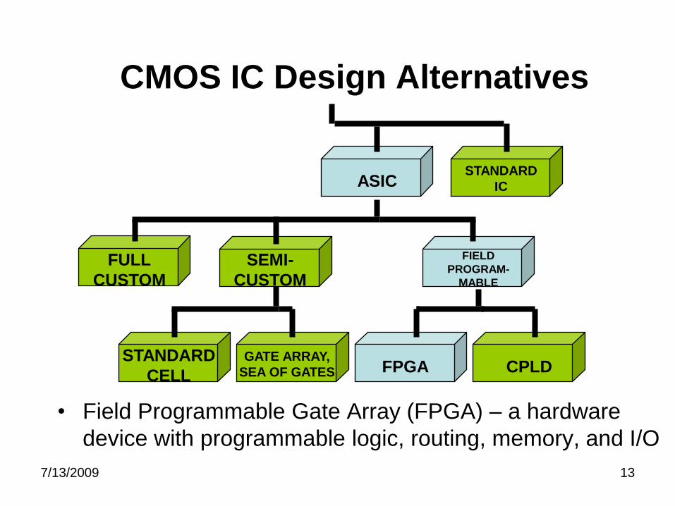
CMOS IC Design Alternatives
STANDARD
IC
FULL
CUSTOM
SEMI-
CUSTOM
FIELD
PROGRAM-
MABLE
STANDARD
CELL
GATE ARRAY,
SEA OF GATES CPLD
ASIC
FPGA
• Field Programmable Gate Array (FPGA) – a hardware
device with programmable logic, routing, memory, and I/O
7/13/2009 14
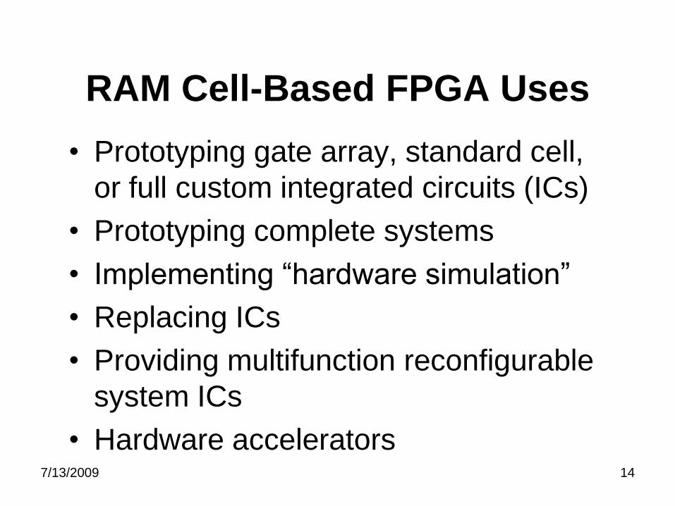
RAM Cell-Based FPGA Uses
• Prototyping gate array, standard cell,
or full custom integrated circuits (ICs)
• Prototyping complete systems
• Implementing “hardware simulation”
• Replacing ICs
• Providing multifunction reconfigurable
system ICs
• Hardware accelerators
7/13/2009 15
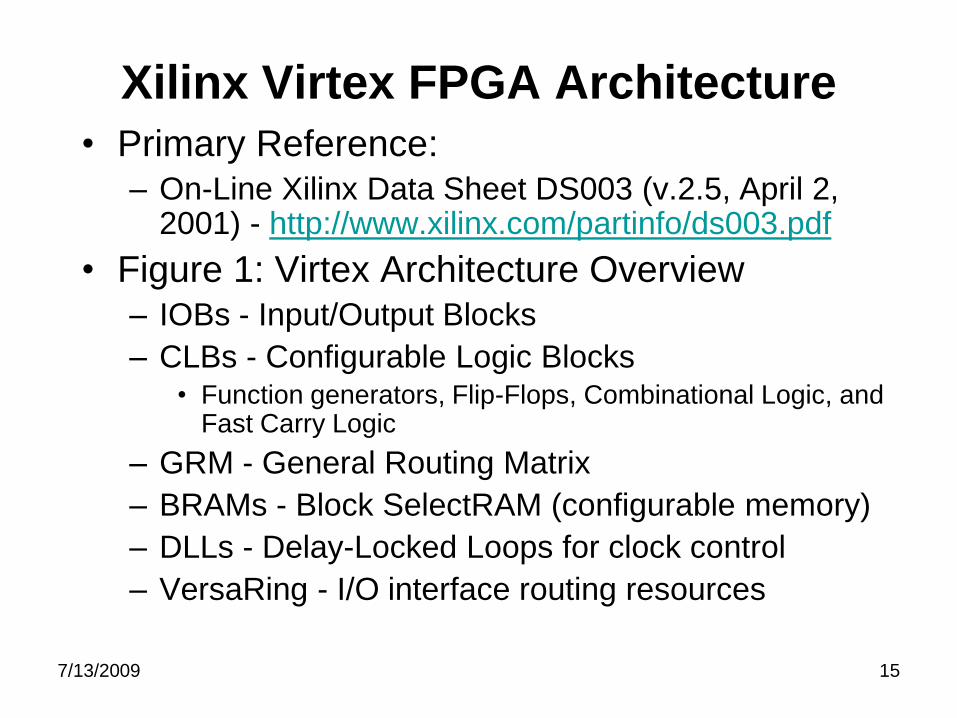
• Primary Reference:– On-Line Xilinx Data Sheet DS003 (v.2.5, April 2,
2001) - http://www.xilinx.com/partinfo/ds003.pdf
• Figure 1: Virtex Architecture Overview– IOBs - Input/Output Blocks
– CLBs - Configurable Logic Blocks• Function generators, Flip-Flops, Combinational Logic, and
Fast Carry Logic
– GRM - General Routing Matrix
– BRAMs - Block SelectRAM (configurable memory)
– DLLs - Delay-Locked Loops for clock control
– VersaRing - I/O interface routing resources
Xilinx Virtex FPGA Architecture
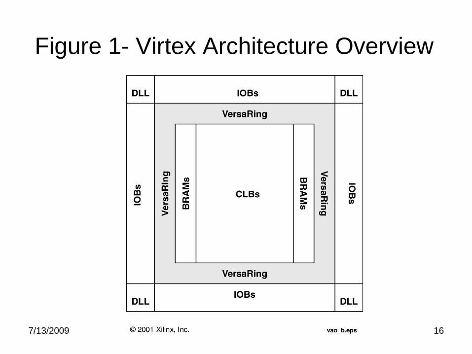
7/13/2009 16
Figure 1- Virtex Architecture Overview
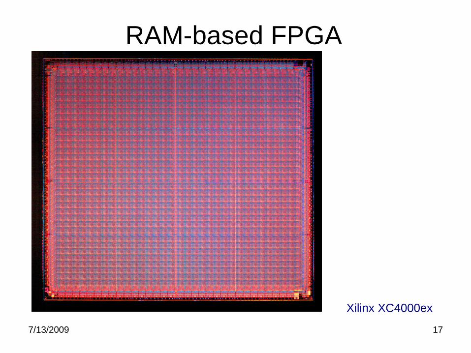
RAM-based FPGA
7/13/2009 17
Xilinx XC4000ex
7/13/2009 18
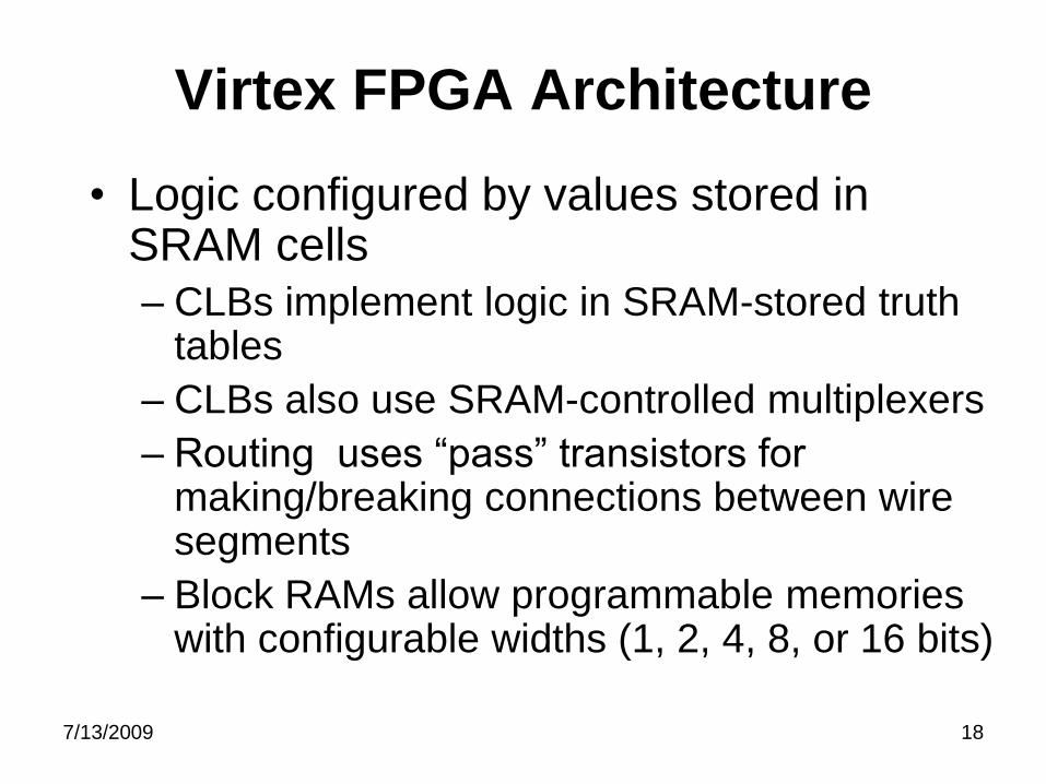
• Logic configured by values stored in SRAM cells
– CLBs implement logic in SRAM-stored truth tables
– CLBs also use SRAM-controlled multiplexers
– Routing uses “pass” transistors for making/breaking connections between wire segments
– Block RAMs allow programmable memories with configurable widths (1, 2, 4, 8, or 16 bits)
Virtex FPGA Architecture
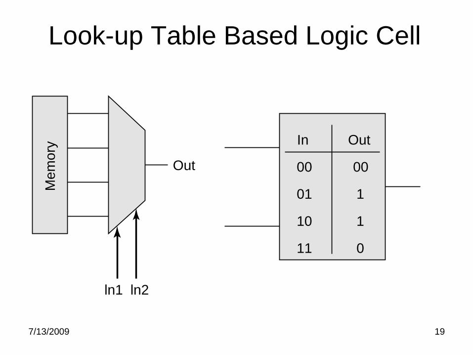
Look-up Table Based Logic Cell
7/13/2009 19
Out
ln1 ln2
Mem
ory
In Out
00 00
01 1
10 1
11 0
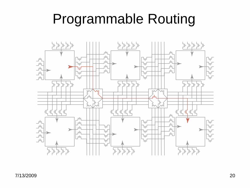
Programmable Routing
7/13/2009 20
7/13/2009 21
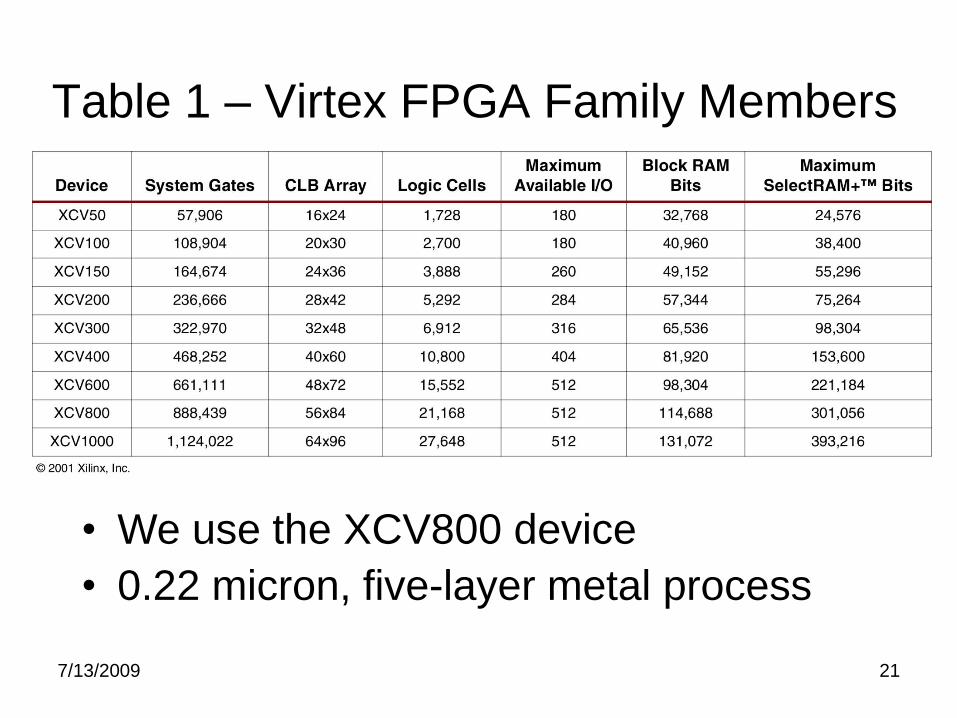
Table 1 – Virtex FPGA Family Members
• We use the XCV800 device
• 0.22 micron, five-layer metal process
7/13/2009 22
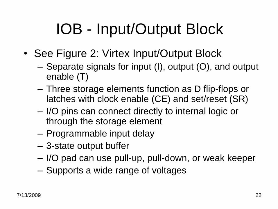
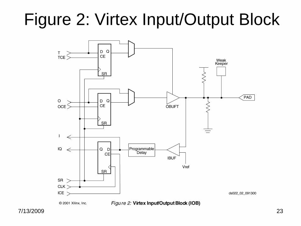
• See Figure 2: Virtex Input/Output Block– Separate signals for input (I), output (O), and output
enable (T)
– Three storage elements function as D flip-flops or latches with clock enable (CE) and set/reset (SR)
– I/O pins can connect directly to internal logic or through the storage element
– Programmable input delay
– 3-state output buffer
– I/O pad can use pull-up, pull-down, or weak keeper
– Supports a wide range of voltages
IOB - Input/Output Block
7/13/2009 23
Figure 2: Virtex Input/Output Block
7/13/2009 24
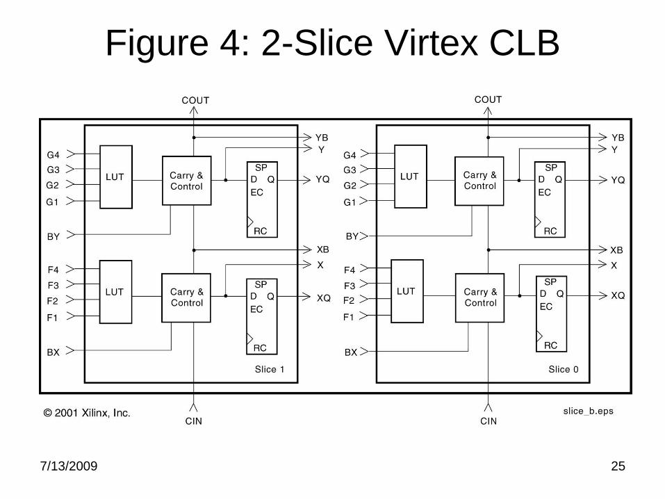
CLB - Configurable Logic Block
• See Figure 4: 2-Slice Virtex CLB
• Each slice contains two logic cells (LCs) and consists of
– 2 4-input look-up tables (LUTs)
– 2 D flip-flops/latches
– Fast carry and control logic
– Three-state drivers
– SRAM control logic
7/13/2009 25
Figure 4: 2-Slice Virtex CLB
7/13/2009 26
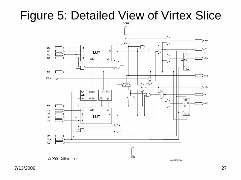
CLB - Configurable Logic Block
• See Figure 5: Detailed View of Virtex Slice
• Logic Function Implementation– 2 Function Generators - Each a 4-input LUT -
implements any 4-input function
– F5 multiplexer - combines two LUTs with select input - implements any 5-input function, 4-to-1 mux, or selected functions of up to 9 inputs.
– F6 multiplexer - combines outputs of two F5 multiplexer - implements any 6-input function, 8-to-1 mux, or selected functions of up to 19 inputs.
– Four direct feedthrough paths - useful to facilitate routing by use of through-the-cell paths
7/13/2009 27
Figure 5: Detailed View of Virtex Slice

7/13/2009 28
CLB - Configurable Logic Block
• Storage Elements
– 2 D flip-flops/latches
– Optionally included in cell output paths
– Shared clock enable
– Shared synchronous/asynchronous Set/Reset
signals
• SR - forces storage element into initialization
state specified (0 or 1)
• BY - forces storage element into opposite state
7/13/2009 29
CLB - Configurable Logic Block
• Fast Carry Logic (See Figures 4 and 5)– Two chains of two bits per CLB
– AND gate (for mult), 0/1 Mux, CY Mux, EXOR
• 3-state Drivers (BUFT) - on-chip drivers with
independent control and input pins
• Distributed LUT SelectRAMs – one per logic cell,
2 LUTs can be reconfigured as one of:• Two 16 x 1-bit synchronous RAM
• 16 x 2-bit synchronous RAM
• 32 x 1-bit synchronous RAM
• 16 x 1-bit dual-port synchronous RAM
• Two 16-bit shift registers
7/13/2009 30
Block SelectRAM• Fully synchronous dual-ported 4096-bit RAM
– Stores address, data and write-control signal on inputs at clock edge
– Cannot change address, even for read, without using clock
– Independent control signals for each port
• Organized in vertical columns of blocks on left and right of CLB array
• Block height is 4 CLBs => Number of block RAMs per column is (height of CLB of array)/4
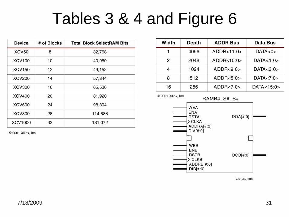
• See Tables 3 & 4 and Figure 6.
7/13/2009 31
Tables 3 & 4 and Figure 6
7/13/2009 32
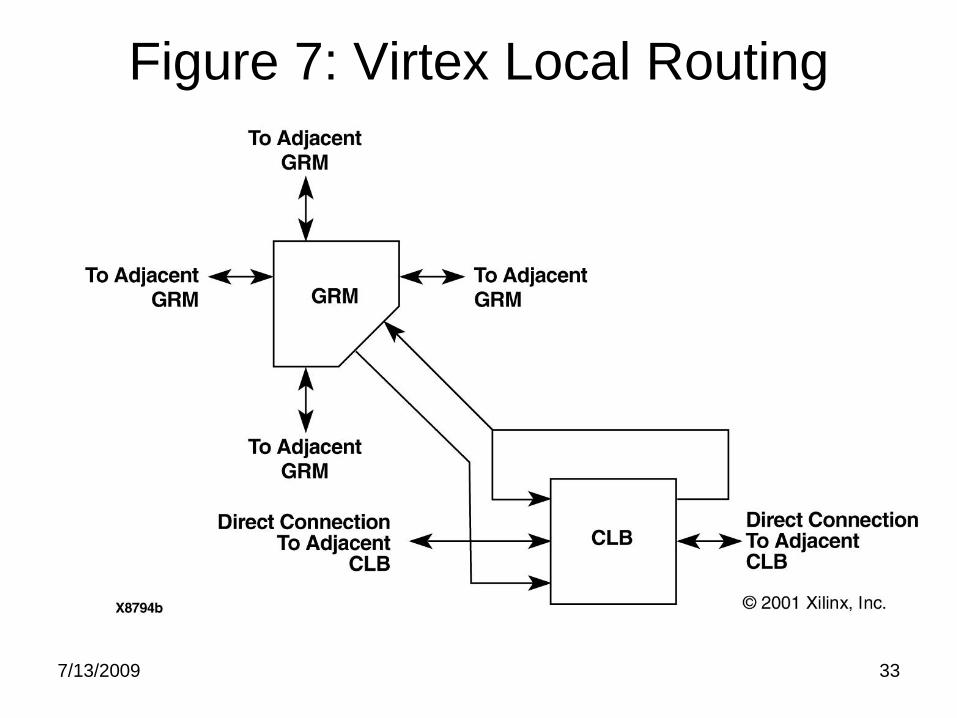
Programmable Routing Matrix• Local Routing
– See Figure 7: Virtex Local Routing
– Interconnections among LUTs, flip-flops, and General Routing Matrix (GRM)
– Internal CLB feedback paths that can chain LUTs together
– Direct paths between horizontally-adjacent CLBs
– Short connections with few “pass” transistors => low delay => high-speed connections
– Combination of hardware and software is used to try to minimize routing delay
7/13/2009 33
Figure 7: Virtex Local Routing
7/13/2009 35
Programmable Routing Matrix
• I/O Routing
– VersaRing
– Supports pin-swapping and pin-locking
– Facilitates pin-out flexibility
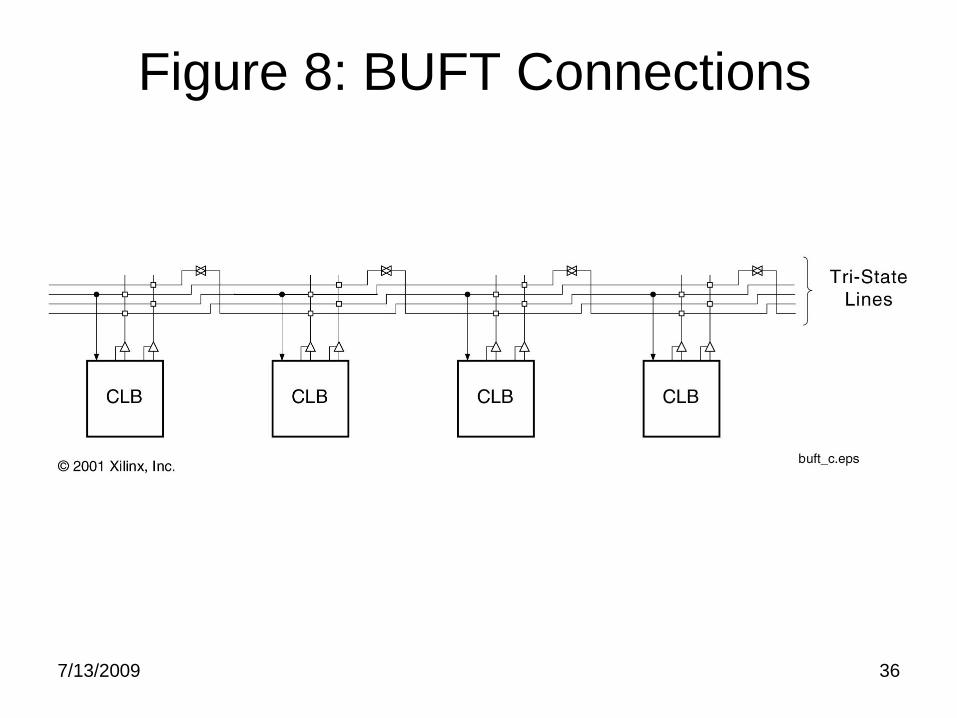
• Dedicated Routing (not programmable)
– Four partitionable bus lines per CLB row driven by
BUFTs (See Figure 8: BUFT Connections)
– Two dedicated nets per CLB for vertical carry
signals to adjacent cells
7/13/2009 36
Figure 8: BUFT Connections
7/13/2009 38
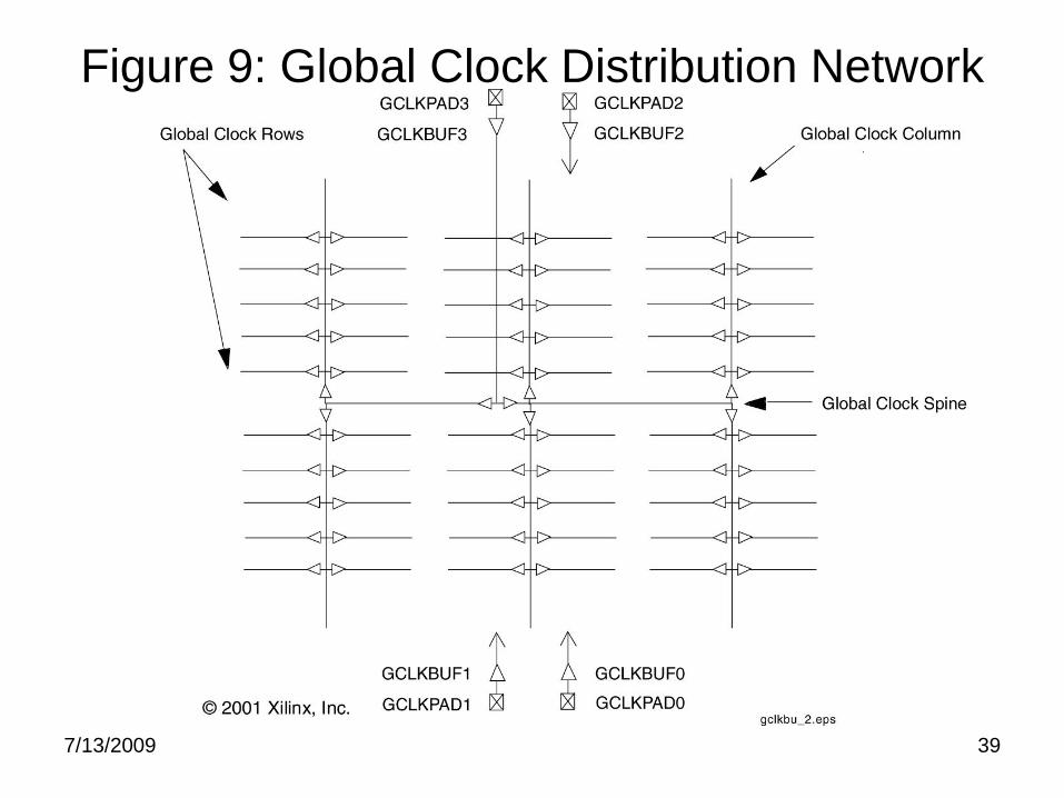
Clock Distribution
• Via primary global routing resources
• See Figure 9: Global Clock Distribution
Network
• Four global buffers
– Two at top center
– Two at bottom center
• Four dedicated clock input pads
• Input to global buffers from pads or from
general purpose routing
7/13/2009 39
Figure 9: Global Clock Distribution Network
7/13/2009 40
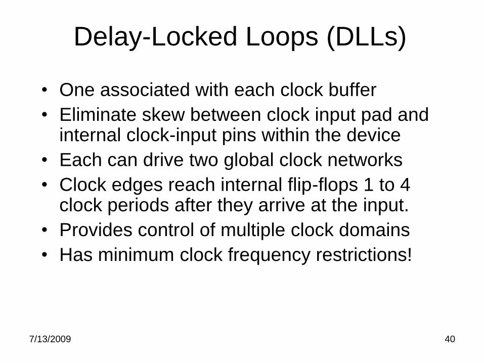
Delay-Locked Loops (DLLs)
• One associated with each clock buffer
• Eliminate skew between clock input pad and internal clock-input pins within the device
• Each can drive two global clock networks
• Clock edges reach internal flip-flops 1 to 4 clock periods after they arrive at the input.
• Provides control of multiple clock domains
• Has minimum clock frequency restrictions!
7/13/2009 41
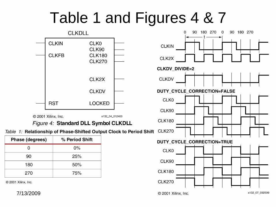
Table 1 and Figures 4 & 7
7/13/2009 43
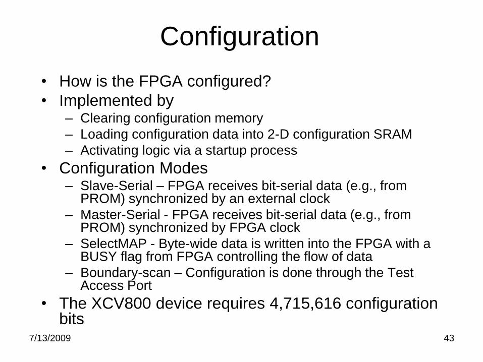
Configuration
• How is the FPGA configured?
• Implemented by – Clearing configuration memory
– Loading configuration data into 2-D configuration SRAM
– Activating logic via a startup process
• Configuration Modes– Slave-Serial – FPGA receives bit-serial data (e.g., from
PROM) synchronized by an external clock
– Master-Serial - FPGA receives bit-serial data (e.g., from PROM) synchronized by FPGA clock
– SelectMAP - Byte-wide data is written into the FPGA with a BUSY flag from FPGA controlling the flow of data
– Boundary-scan – Configuration is done through the Test Access Port
• The XCV800 device requires 4,715,616 configuration bits
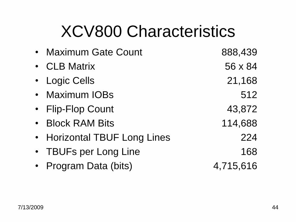
7/13/2009 44
XCV800 Characteristics• Maximum Gate Count 888,439
• CLB Matrix 56 x 84
• Logic Cells 21,168
• Maximum IOBs 512
• Flip-Flop Count 43,872
• Block RAM Bits 114,688
• Horizontal TBUF Long Lines 224
• TBUFs per Long Line 168
• Program Data (bits) 4,715,616
7/13/2009 45
THE ECE 554 XILINX DESIGN
PROCESS
• Design process overview
• Design reference
• Design tutorial
• What’s next
7/13/2009 46
Design Process Steps
• Definition of system requirements.– Example: ISA (instruction set architecture) for
CPU.
– Includes software and hardware interfaces with timing.
– May also include cost, speed, power, reliability and maintainability specifications.
• Definition of system architecture.– Example: high-level HDL (hardware description
language) representation - this is optional in ECE 554, but is done in the real world).
– Useful for system validation and verification and as a basis for lower level design execution and validation or verification.
7/13/2009 47
Design Process Steps(continued)• Refinement of system architecture
– In manual design, descent in hierarchy, designing increasingly lower-level components
– In synthesized design, transformation of high-level HDL to “synthesizable” register transfer level (RTL) HDL
• Logic design or synthesis– In manual or synthesized design, development of
logic design in terms of library components
– Result is logic level schematic or netlist representation or combinations of both.
– Both manual design and synthesis typically involve optimization of cost, area, or delay.
7/13/2009 48
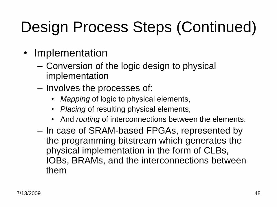
Design Process Steps (Continued)
• Implementation– Conversion of the logic design to physical
implementation
– Involves the processes of:• Mapping of logic to physical elements,
• Placing of resulting physical elements,
• And routing of interconnections between the elements.
– In case of SRAM-based FPGAs, represented by the programming bitstream which generates the physical implementation in the form of CLBs, IOBs, BRAMs, and the interconnections between them
7/13/2009 49
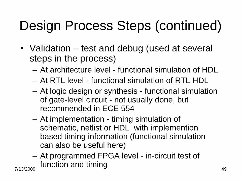
Design Process Steps (continued)
• Validation – test and debug (used at several steps in the process)– At architecture level - functional simulation of HDL
– At RTL level - functional simulation of RTL HDL
– At logic design or synthesis - functional simulation of gate-level circuit - not usually done, but recommended in ECE 554
– At implementation - timing simulation of schematic, netlist or HDL with implemention based timing information (functional simulation can also be useful here)
– At programmed FPGA level - in-circuit test of function and timing
7/13/2009 50
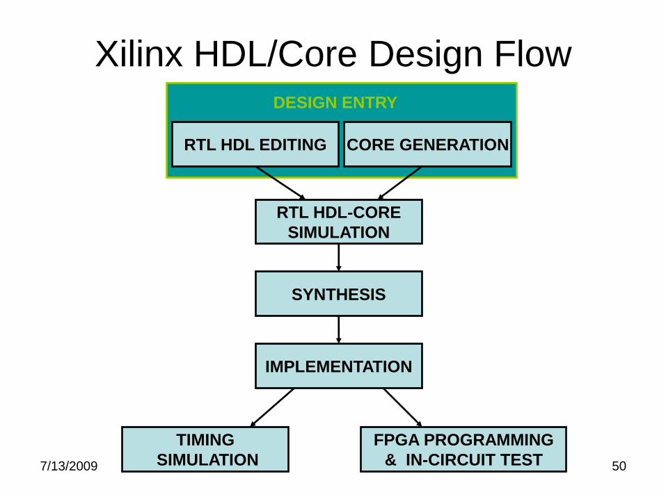
Xilinx HDL/Core Design FlowDESIGN ENTRY
CORE GENERATIONRTL HDL EDITING
RTL HDL-CORE
SIMULATION
SYNTHESIS
IMPLEMENTATION
TIMING
SIMULATION
FPGA PROGRAMMING
& IN-CIRCUIT TEST
7/13/2009 51
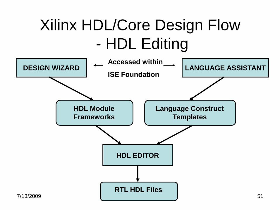
Xilinx HDL/Core Design Flow
- HDL Editing
Language Construct
Templates
HDL EDITOR
DESIGN WIZARD LANGUAGE ASSISTANTAccessed within
ISE Foundation
RTL HDL Files
HDL Module
Frameworks
7/13/2009 52
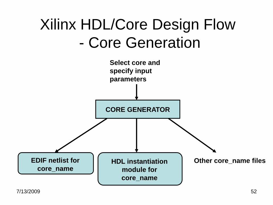
Xilinx HDL/Core Design Flow
- Core Generation
CORE GENERATOR
Select core and
specify input
parameters
HDL instantiation
module for
core_name
EDIF netlist for
core_nameOther core_name files
7/13/2009 53
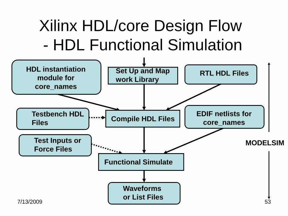
Xilinx HDL/core Design Flow
- HDL Functional Simulation
Compile HDL Files
Waveforms
or List Files
Set Up and Map
work LibraryRTL HDL Files
Test Inputs or
Force Files
HDL instantiation
module for
core_names
EDIF netlists for
core_names
Functional Simulate
Testbench HDL
Files
MODELSIM
7/13/2009 54
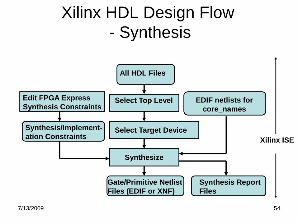
All HDL Files
Gate/Primitive Netlist
Files (EDIF or XNF)
Xilinx HDL Design Flow
- Synthesis
Select Top Level
Select Target Device
Edit FPGA Express
Synthesis Constraints
Synthesize
Synthesis/Implement-
ation Constraints
Synthesis Report
Files
EDIF netlists for
core_names
Xilinx ISE
7/13/2009 55
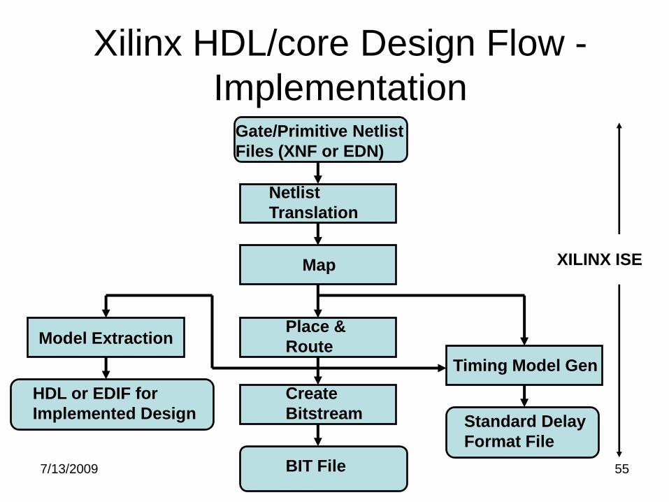
Model Extraction
Xilinx HDL/core Design Flow -
Implementation
Netlist
Translation
Map
Place &
Route
BIT File
Create
Bitstream
Timing Model Gen
Gate/Primitive Netlist
Files (XNF or EDN)
Standard Delay
Format File
HDL or EDIF for
Implemented Design
XILINX ISE
7/13/2009 56
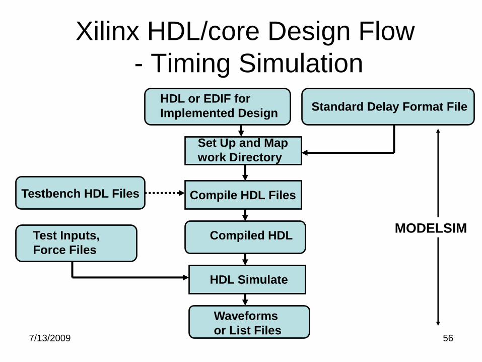
Xilinx HDL/core Design Flow
- Timing Simulation
Test Inputs,
Force Files
MODELSIM
Compile HDL Files
Waveforms
or List Files
Set Up and Map
work Directory
Compiled HDL
HDL Simulate
Standard Delay Format FileHDL or EDIF for
Implemented Design
Testbench HDL Files
7/13/2009 57
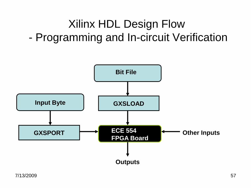
Xilinx HDL Design Flow
- Programming and In-circuit Verification
Bit File
ECE 554
FPGA Board
GXSLOAD
GXSPORT
Input Byte
Other Inputs
Outputs
7/13/2009 58
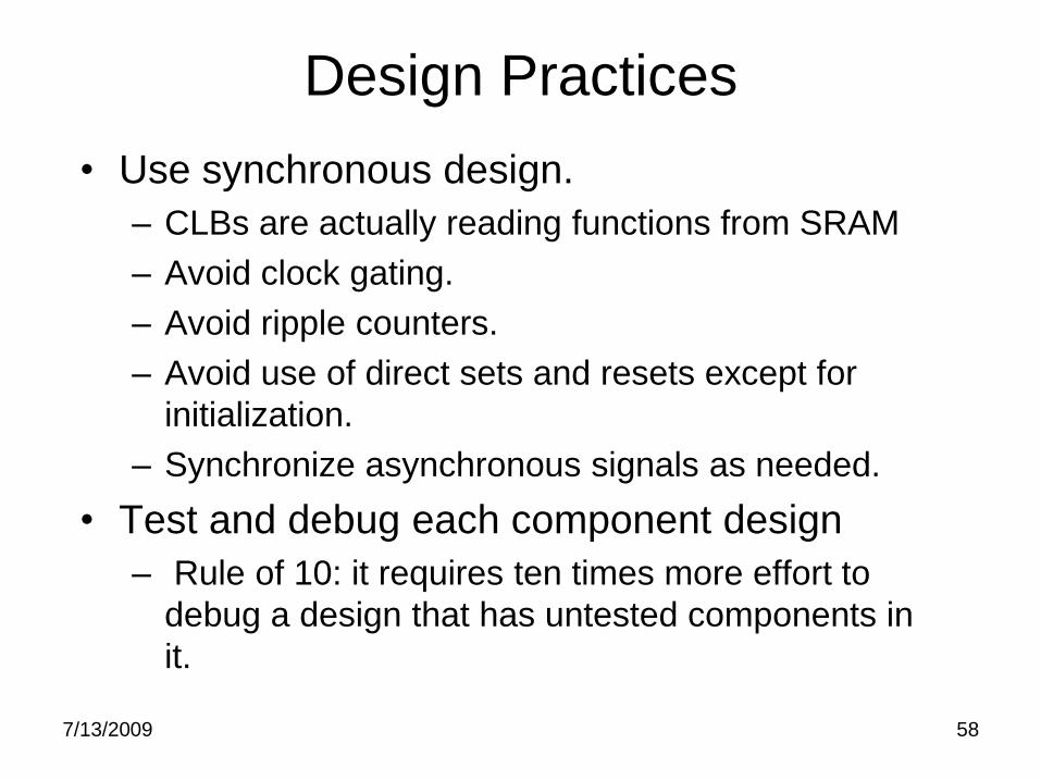
Design Practices
• Use synchronous design.
– CLBs are actually reading functions from SRAM
– Avoid clock gating.
– Avoid ripple counters.
– Avoid use of direct sets and resets except for
initialization.
– Synchronize asynchronous signals as needed.
• Test and debug each component design
– Rule of 10: it requires ten times more effort to
debug a design that has untested components in
it.
7/13/2009 59
What’s Next
• HDL/core design flow – design tutorial will
employ the flow described for a Verilog
HDL/core example
– During lab time on Tuesday
– https://cgi.cae.wisc.edu/~ece554/pmwiki/pmwiki.php?
n=Documentation.Tutorial
– Read over the tutorial before coming to lab
• Find a partner for the miniproject by next
Tuesday
• Start looking over the course website
– If you feel rusty with Verilog, take a look at lecture 2
7/13/2009 60
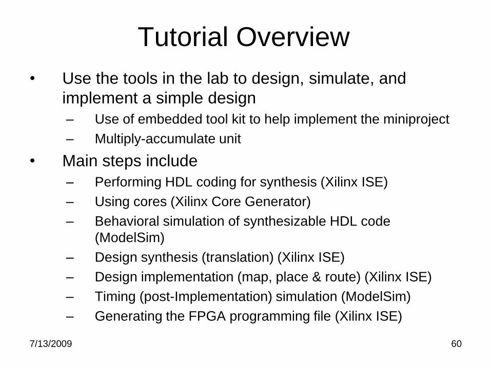
Tutorial Overview
• Use the tools in the lab to design, simulate, and
implement a simple design
– Use of embedded tool kit to help implement the miniproject
– Multiply-accumulate unit
• Main steps include
– Performing HDL coding for synthesis (Xilinx ISE)
– Using cores (Xilinx Core Generator)
– Behavioral simulation of synthesizable HDL code
(ModelSim)
– Design synthesis (translation) (Xilinx ISE)
– Design implementation (map, place & route) (Xilinx ISE)
– Timing (post-Implementation) simulation (ModelSim)
– Generating the FPGA programming file (Xilinx ISE)


![Design Considerations for Next Generation Wireless Power ......[Montanaro, JSSC ‘96] CLB CLB CLB CLB 65% 21% 9% 5% Interconnect Clock I/O CLB “Software” Energy Dissipation is](https://img.pdfslide.us/doc/110x75/6075f305565b1e4d845c5e4e/design-considerations-for-next-generation-wireless-power-montanaro-jssc.jpg)