Embed Size (px)
Citation preview
Dynamic Article LinksC<Journal ofMaterials Chemistry
Cite this: J. Mater. Chem., 2012, 22, 6104
www.rsc.org/materials PAPER
Publ
ishe
d on
16
Febr
uary
201
2. D
ownl
oade
d by
BR
UN
EL
UN
IVE
RSI
TY
on
13/1
1/20
13 1
5:10
:31.
View Article Online / Journal Homepage / Table of Contents for this issue
Novel lithium Schiff-base cluster complexes as electron injectors: synthesis,crystal structure, thin film characterisation and their performance in OLEDs†
Poopathy Kathirgamanathan,*a Sivagnanasundram Surendrakumar,a Juan Antipan-Lara,a
Seenivasagam Ravichandran,a Y. F. Chan,a Vincent Arkley,a Subramanium Ganeshamurugan,a
Muttulingham Kumaraverl,a Gnanamoly Paramswara,a Arumugam Partheepan,a Vanga R. Reddy,a
Daniel Baileyb and Alexander J. Blake*b
Received 10th October 2011, Accepted 9th January 2012
DOI: 10.1039/c2jm15114f
A set of novel lithium Schiff base cluster compounds has been synthesised and characterised for the first
time and tested as electron injectors in OLED devices. Their electrical, electronic, thermal and optical
properties have been investigated and compared with the industry standards LiF and lithium
quinolinolate (LiQ). Amongst the compounds tested, lithium 2-((o-tolylimino)methyl) phenolate was
found to enhance the efficiency of OLEDs by 69% compared to LiF and 15% compared to LiQ. The
same electron injector was found to extend the lifetimes of OLEDs by six-fold compared to LiF and 4.3-
fold compared to LiQ respectively. The crystal structure of the parent compound, lithium 2-
((phenylamino)methyl)phenolate reveals that the compound is tetrameric in contrast to hexameric LiQ.
Substituting the methyl group with fluorine causes a remarkable depression of the HOMO and LUMO
levels by up to 1.2 eV. Analysis of current density vs. voltage characteristics of single-layer devices for
Li–Al/electron injector/Li–Al and Al/electron injector/Al reveals that both sets of devices are operating
as electron-only devices indicating that the formation of free lithium is the cause of enhanced electron
injection, but either the energetic aluminium atoms (as proposed previously by other workers) or
energetic lithium complexes on an aluminium surface (as we have demonstrated in this paper) are all
that is required for efficient electron injection.
Introduction
Organic light emitting diodes have been the subject of intense
investigation due to their increasing applications in displays (e.g.,
Samsung mobile phones, Sony’s AM-OLED TV) and lighting
(Philips, Osram and Pioneer).1–4 The recent announcement by
Samsung of its intention to invest 2.2 billion US Dollars into
active matrix OLED television (AM-OLED) to bring it into the
mainstream TV market has given considerable impetus to the
scientists developing materials for the OLED devices.
OLEDs are multilayer devices, typically composed of (i) a hole
injector (e.g., copper phthalocyanine (CuPc), 4,40,40 0-tris[N-(2-
naphthyl)-N-phenyl-amino)-triphenylamine (2-TNATA), tri-
pyrazinocyclohexane(s);1–3 (ii) a hole transporter (e.g., N,N0-bis-(1-naphthalenyl)-N,N0-bis-phenyl-(1,10-biphenyl)-4,40-diamine,
a-NPB); (iii) an emissive layer (host + dopant); (iv) an electron
aOrganic Electronics, Wolfson Centre, Brunel University, Uxbridge, UB83PH, UK. E-mail: [email protected] of Chemistry, The University of Nottingham, University Park,Nottingham, NG7 2RD, UK
† Electronic supplementary information (ESI) available. CCDCreference number 847975. For ESI and crystallographic data in CIF orother electronic format see DOI: 10.1039/c2jm15114f
6104 | J. Mater. Chem., 2012, 22, 6104–6116
transporter (e.g., tris(8-hydroxyquinoline)-aluminium (Alq3));
(v) an electron injector (e.g., LiF, CsF, lithium quinolinolates)
and (vi) a cathode (e.g., Al)4–6 to provide charge balance so that
efficient devices can be produced. Hole transporters and electron
transporters can also be doped with an acceptor or donor,
respectively, to increase the conductivities of the respective
layers.5-7
There are continuing demands for reductions in the operating
voltage and power consumption of OLEDs, while achieving
increased lifetimes is also a priority. Charge transport (hole and
electron) materials, whether pure or doped, are an integral part
of any OLED. It has been reported9 that nearly 60% of the total
electrical power is lost through the charge transport layers, of
which nearly 36% is through the electron transporting layer,
5.7% through the electron injecting layer and the remainder
through the hole injection layer, hole transporting layer and the
hole blocking layer. The lifetime is also critically dependent on
the nature of the charge transporters employed. Improvements in
efficiencies of up to 70% have been reported in otherwise iden-
tical devices by Kathirgamanathan et al.2 and Kido et al.8 when
Alq3 is replaced by novel electron transporters.
In order to produce an efficient OLED, the anode should have
as high a work function (W.F.) as possible so that the barrier for
This journal is ª The Royal Society of Chemistry 2012

Publ
ishe
d on
16
Febr
uary
201
2. D
ownl
oade
d by
BR
UN
EL
UN
IVE
RSI
TY
on
13/1
1/20
13 1
5:10
:31.
View Article Online
the hole injection is minimised, while the cathode should have as
low a work function as possible so that the barrier for electron
injection is reduced.10–12 Despite its high work function (W.F.) of
4.2 eV, aluminium has been widely used as a cathode because of
its reasonably high air stability and ease of deposition.
In 1976, Partridge employed low work function Cs metal
(W.F.¼ 2.0 eV) as an efficient cathode13 on polymer OLEDs and
later Tang and Van Slyke14,15 employed a Mg/Ag alloy (W.F. ¼3.7 eV). This was followed by the use of low work function Ca
and Ba electrodes by Burroughes et al. in 1990 (ref. 16). All these
low work function metals are extremely sensitive to moisture and
oxygen and therefore not very practical in an industrial
manufacturing environment. In 1997, Kido et al. demonstrated
the use of a stable Li/Al alloy (W.F. ¼ 2.8 eV) as a cathode,
significantly reducing the operating voltage.17 In the same year,
Wakimoto et al.18 showed that various alkali metal compounds
(e.g., Li2O, Cs2O, NaCl, KCl and RbCl) in conjunction with an
Al cathode were as effective as the Li/Al alloy as far as the
electron injection is concerned, effecting a three-fold improve-
ment in efficiency and a 35% reduction in operating voltage.
It was also noteworthy that the lifetimes of OLED devices with
Li/Al or Li2O/Al cathodes were three times as long as those with
Mg/Al cathodes.18
The reduction in operating voltage from lithium compounds
or alloys is due to the low work function of this metal (W.F. ¼2.2 eV). The use of Li/Al alloys does not always result in
reproducible devices under large scale manufacturing vacuum
evaporation conditions: this is because they contain varying
compositions of the individual metals as a result of these
exhibiting different vapour pressures and densities. To alleviate
this problem, Hung et al. employed a thin layer of LiF (0.1–1 nm)
as an electron injector and found that the reduction in operating
voltage was comparable to that obtained with Li/Al alloys.19
Hung et al.19 examined the Alq3/LiF/Al interface of the device
(ITO/a-NPB (75 nm)/Alq3 (70 nm)/LiF (0.3 nm)/Al (100 nm)) by
high resolution electron energy loss spectroscopy (HREELS) and
postulated that the mechanism for reduction in operating voltage
compared to the Alq3/Al interface involves the formation of free
Li metal at the organics/Al interface, thereby reducing the W.F.
Interfacial studies by synchrotron radiation photoemission
spectroscopy revealed that there is a reaction between LiF and
the highly reactive aluminium atoms produced during vacuum
thermal evaporation.19,20 On this basis, Hung et al. proposed the
following interfacial reaction which is claimed to be thermody-
namically feasible:19,20
3LiF + Al + 3Alq3 / AlF3 + 3Li+Alq3� (1)
However, Wong et al.21 reported the use of LiF to reduce the
W.F. of diamond surfaces via the dipole effect induced by LiF
(which has a very high dipole moment of 6.33� 0.63 Debye). For
example, the W.F. of the hydrogenated diamond decreased from
4.4 eV (virgin) to 2.4 eV on depositing 1.5 nm of LiF and the
W.F. of oxygenated diamond dropped from 3.6 eV to 2.4 eV. The
question therefore arises of whether the reaction given in eqn (1)
is critical for the reduction in the operating voltage in an OLED
device.
Moreover, LiF has three major drawbacks: (a) it is an insu-
lator and thus the thickness of the deposit has to be kept below
This journal is ª The Royal Society of Chemistry 2012
1 nm so that the operating voltage does not increase; (b) it
requires very high temperatures (500–600 �C) to evaporate even
under high vacuum, requiring expensive crucibles; (c) it is
hygroscopic.
To alleviate the problems with LiF, complexes such as lithium
quinolinolate (LiQ, EI-101) have been employed as electron
injectors with considerable success even on an industrial scale
because: (a) it evaporates at much lower temperatures (200–300�C); (b) it is air stable; and (c) it is not hygroscopic.
We first reported the synthesis of thermally stable, solvent-
free and sublimable high purity LiQ22 which was later struc-
turally characterised as hexameric (Liq)6 by X-ray diffrac-
tion.23 The oligomeric nature (clusters) of lithium complexes
explains their low evaporation temperatures and air stability.
Indeed, most lithium complexes occur as cluster compounds:
for example lithium(2-methyl-8-hydroxyquinolinolate) is a hex-
amer while lithium(2-phenyl-8-hydroxyquinolinolate) is
a tetramer.24
(Liq)6 has been found to be a good electron injector as well as
a good host material in some cases, but does not function as an
effective electron transporter because of its poor electrical
conductivity (<1 � 10�11 S cm�1). However, it has been used as
an admixture in conjunction with other electron transporters
such as Alq3, Zrq4 and some anthracene derivatives25 to modu-
late the electron mobility and enhance the lifetime. However, no
data on lifetime or voltage drift have been reported where LiQ
was employed as an electron injector or in an admixture with any
electron transporters.
Several other complexes of lithium, namely, 2,3-diphenyl-5-
hydroxyquinoxalinatolithium and lithium(hydroxy-
phenylbenzoxazole(s) have also been found to act as good
electron injectors.10,26,27 It is noteworthy that while Pu et al.28
have reported the potential use of some lithium complexes [e.g.,
lithium 2-(20,20 0-bipyridine-60-yl)phenolate (LiBPP), lithium-
2-(isoquinoline-10-yl)phenolate (LiIQP)] as very efficient electron
injectors-cum-electron transporters; their effects on the lifetime
(an important parameter) of the devices have not been disclosed,
thereby questioning their wide applicability. Related compounds
have also been published by Sun et al., but again no lifetime data
were provided.33
Although LiQ has been used since the 1960’s,29 a recent toxi-
cological study employing the Ames Test30–32 showed that LiQ
exhibits mutagenic activity (70 mg per plate, in the histidine-
dependent auxotropic mutant Salmonella typhimurium, Strain
TA100).30–32
We have been interested in OLED materials in general and
electron injectors in particular for the past 18 years, during which
period we made a large number of lithium complexes in our quest
for non-toxic (or less toxic) electron injectors with superior
performance to LiQ. This paper describes the synthesis of lithium
complexes (clusters) of some selected Schiff bases (reaction
scheme shown below) from a large number of complexes made by
us and their performance in OLEDs in comparison to the
industrial standard LiF and LiQ for the first time. We also
examine their mechanism of conduction and carrier injection,
and their effect on the lifetime and the voltage drift during device
operation. This paper also investigates the interactions of these
novel compounds with the electrode (Al) and the electron
transporter (Zrq4).
J. Mater. Chem., 2012, 22, 6104–6116 | 6105
Scheme 2 Synthesis of lithium quinolinolate.
Table 1 Synthetic and sublimation yields for lithium Schiff-basecomplexes
Material Synthetic yield (%) Sublimation yield (%)
EI-101 (LiQ) 95 88EI-111 97 30EI-111-2Me 93 75EI-111-3Me 87 30EI-111-4Me 75 30
Publ
ishe
d on
16
Febr
uary
201
2. D
ownl
oade
d by
BR
UN
EL
UN
IVE
RSI
TY
on
13/1
1/20
13 1
5:10
:31.
View Article Online
Experimental
The lithium complexes were prepared by the following general
route: (Schemes 1 and 2).
The lithium Schiff-base complexes reported herein have been
made in 20 g quantities and triply sublimed to give 99.9% purity
materials. Although the synthetic yield of the reaction is between
75 and 95% for analytically pure samples, the sublimation yields
(Table 1) were substantially different. EI-111-2Me was found to
give the highest sublimation yield.
Device fabrications and measurements
Electron-only devices were fabricated by evaporating the elec-
tron injectors (EI-101 (LiQ), EI-111 or EI-111-2Me) to produce
a layer thickness of 40–50 nm onto Li–Al (2 : 98) alloy coated
ITO/glass and sandwiching it with a bottom contact of another
layer of Li–Al alloy (200 nm) (System A). Other single-layer
devices with Al or ITO as the anode and Al, Li–Al or Au as the
cathode have been constructed in order to investigate the
dependence of work function on the mechanism of conduction:
these are devices of the type ITO/EI/Al (mixed conduction,
System C), ITO/EI/Au (hole-only, System D) and ITO/Al/EI/Al
(System B) to test the effect of Al interaction on EI (to be dis-
cussed later).
Electroluminescent devices were fabricated by thermal evap-
oration using a multi-chamber OLED pilot plant machine (Sol-
ciet, manufactured by ULVAC, Japan). The devices were
fabricated on a patterned (pixelated) ITO substrate (surface
resistance of 40U per square Hitachi High Tech., Japan), cleaned
with water, acetone, isopropyl alcohol and water (in that order),
then dried at 150 �C for 20 minutes and then subjected to ozone
cleaning (UV irradiation, 185 nm) at 150 �C for 10 minutes. The
substrate was then plasma-cleaned in the presence of oxygen for
25 seconds and moved into the vacuum chamber from which the
hole injector [(5,10,15,20-tetra(p-tolyl)-21H,23H-porphine)
Scheme 1 Synthesis of lithium (phenyliminomethyl)phenolate deriva-
tives EI-111 (R ¼ H); EI-111-2Me (R ¼ 2Me); EI-111-3Me (R ¼ 3Me),
EI-111-4Me (R¼ 4Me) EI-111-2F (R¼ 2F); EI-111-3F (R¼ 3F) and EI-
111-4F (R ¼ 4F).
6106 | J. Mater. Chem., 2012, 22, 6104–6116
zinc(II) (ZnTPTP), 20 nm], hole transporter [N,N0-bis(1-naph-thalenyl)-N,N0-bis-phenyl-(1,10-biphenyl)-4,40-diamine (a-NPB),
50 nm], host : dopant [Alq3 (50 nm) : (0.1 nm) dopant (N,N0-diphenylquinacridone) (DPQA), co-evaporation], electron
transporter [either Alq3 or Zrq4, 20 nm] were sequentially
deposited. The evaporation rates of ZnTPTP, a-NPB, (Alq3,
DPQA), Zrq4 and LiF (electron injector) were 1 �A s�1, 1.5 �A s�1,
(1 �A s�1, 0.1 �A s�1), 0.05 �A s�1 respectively. The evaporation rates
of LiQ, EI-111 and EI-111-2Me were 0.5 �A s�1.
Directly from the vacuum chamber all the devices were
encapsulated with a UV curable adhesive (Nagase) onto glass
backplates in a glovebox filled with dry nitrogen so that the
device is not exposed to air. The electrical and optical measure-
ments were carried out by a computer-controlled Keithley 2400
Source Meter and a Minolta (CS-1000) spectrometer, respec-
tively. HOMO–LUMO levels were determined by cyclic vol-
tammetry (by computer-controlled potentiostat PAR 273 or CHI
600D) and from band gap measurements by absorption spec-
troscopy of thin films produced by vacuum thermal evaporation.
Capacitance measurements were made on thin films as well as
compacted discs using an Impedance Analyser (Hewlett Packard,
4284A). DC conductivity measurements of the materials were
also performed on compacted discs using a two-probe method.35
Crystal structure determination
Single crystals of EI-111 suitable for single-crystal X-ray crys-
tallographic studies were grown by slow vacuum sublimation at
a temperature of 275 �C and a pressure of 5 � 10�6 Torr.
Crystal data for EI-111. C52H40Li4N4O4, M ¼ 812.64, mono-
clinic, space group P21/c, a ¼ 10.4110(14), b ¼ 17.316(2), c ¼24.493(3)�A, b¼ 97.918(2)�,U¼ 4373.4(9)�A3, T¼ 150(2) K,Z¼4, Dc ¼ 1.234 Mg m�3, m(Mo-Ka) ¼ 0.077 mm�1, 7787 unique
reflections (Rint ¼ 0.048). Final R1 [5302 F $ 4s(F)] ¼ 0.0349,
wR2 (all data) ¼ 0.0861.
Results and discussion
Crystal structure
In the crystal, EI-111 was found to be tetrameric and to adopt a
slightly distorted Li4O4 cubane-type structure (Fig. 1) with Li–O
This journal is ª The Royal Society of Chemistry 2012
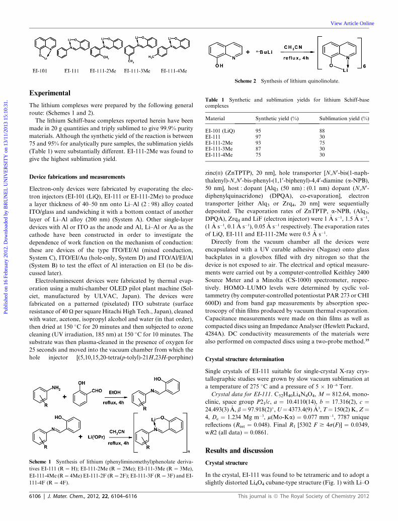
Fig. 1 Crystal structure of lithium 2-((phenylimino)methyl)phenolate
(EI-111). Displacement ellipsoids are drawn at the 20% probability level
and hydrogen atoms are omitted for clarity.
Table 2 Cluster size determination by mass spectroscopy (MS) andcrystal structure analysis (XRD)
CompoundNo. of units inthe cluster by MS
No. of units in thecluster by XRD
EI-101 (LiQ) 6 6EI-111 4 4EI-111-2Me 3 Not availableEI-111-3Me 3 Not availableEI-111-4Me 4 Not available
Fig. 2 Differential scanning calorimetry of EI-101 (LiQ), EI-111, EI-
111-2Me, EI-111-3Me, EI-111-4Me under nitrogen atmosphere. Scan
rate: 30 �C per minute.
Publ
ishe
d on
16
Febr
uary
201
2. D
ownl
oade
d by
BR
UN
EL
UN
IVE
RSI
TY
on
13/1
1/20
13 1
5:10
:31.
View Article Online
distances of 1.902(3)–1.978(3) �A, O–Li–O angles of 93.59(12)–
97.09(12)� and Li–O–Li angles of 83.22(11)–85.85(11)�; Li–N
distances external to the Li4O4 cube span the range 1.966(3)–
1.993(3) �A. Each of the four ligands therefore contributes one
oxygen atom to the formation of the cubane via an LiO4 apex,
with its nitrogen donor atom providing the cap of an adjacent
LiO4N apex. As a result, four of the eight Li–O edges are bridged
by a ligand. The individual ligands deviate significantly from
planarity, with the dihedral angles between their phenyl rings
ranging from 29.00(7) to 54.49(8)�. The structure does not exhibitspecific directional intermolecular interactions, but layers of
molecules are strongly interdigitated. (Fig. EI-111_PACK_-
A.PNG and EI-111_PACK_C.PNG, see ESI†.)
Fig. 3 Thermogravimetry of EI-101 (LiQ), EI-111, EI-111-2Me, EI-111-
3Me, EI-111-4Me under nitrogen atmosphere.
Cluster size
Unlike the crystal structure of EI-111 which is tetrameric (see
above), that of EI-101 (LiQ) is hexameric [(Liq)6].23 We
employed mass spectroscopy to establish the number of units
present in each cluster. Although mass spectroscopy is a gas
phase measurement, it gives useful information as to the cluster
size. Further, it also confirms that layers of these materials
produced on thermal evaporation are composed of clusters.
This journal is ª The Royal Society of Chemistry 2012
Table 2 shows the results from both mass spectroscopy and
crystal structure where available.
Physical characteristics
Thermal properties. Thermal properties were measured by
differential scanning calorimetry (DSC) (Fig. 2) and thermog-
ravimetric analysis (TGA) (Fig. 3). The results are summarised in
Table 3.
As can be seen from Table 3, only LiQ shows a Tg, although
none of the lithium Schiff-base complexes reported here do. The
lithium complexes with 2,3-dimethylaniline and 2,4-dimethyl
aniline Schiff bases exhibit Tg values of 111 �C and 95 �C,respectively, whereas the 2,5-dimethyl derivative does not exhibit
a Tg.43
TGA studies show that with one exception, namely
EI-111-3Me, all the electron injectors are stable up to 260 �C.EI-111-3Me is only stable up to 150 �C. EI-101 and EI-111-4Me
show monophasic decomposition whereas EI-111, EI-111-2Me,
EI-111-3Me show biphasic decomposition patterns. Initial
J. Mater. Chem., 2012, 22, 6104–6116 | 6107
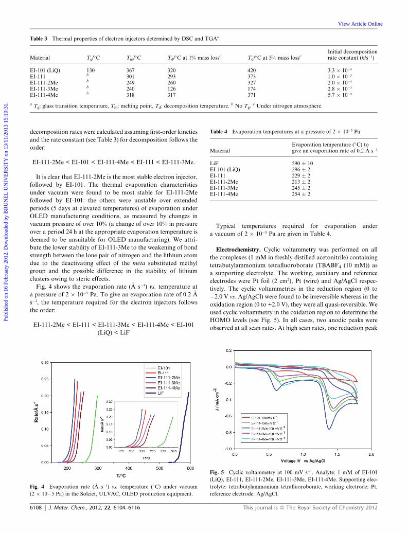
Table 3 Thermal properties of electron injectors determined by DSC and TGAa
Material Tg/�C Tm/
�C Td/�C at 1% mass lossc Td/
�C at 5% mass losscInitial decompositionrate constant (k/s�1)
EI-101 (LiQ) 130 367 320 420 3.3 � 10�4
EI-111 b 301 293 373 1.0 � 10�3
EI-111-2Me b 249 260 327 2.0 � 10�4
EI-111-3Me b 240 126 174 2.8 � 10�3
EI-111-4Me b 318 317 371 5.7 � 10�4
a Tg: glass transition temperature, Tm: melting point, Td: decomposition temperature. b No Tg.c Under nitrogen atmosphere.
Table 4 Evaporation temperatures at a pressure of 2 � 10�5 Pa
MaterialEvaporation temperature (�C) togive an evaporation rate of 0.2 �A s�1
LiF 590 � 10EI-101 (LiQ) 296 � 2EI-111 229 � 2EI-111-2Me 213 � 2EI-111-3Me 245 � 2EI-111-4Me 254 � 2
Publ
ishe
d on
16
Febr
uary
201
2. D
ownl
oade
d by
BR
UN
EL
UN
IVE
RSI
TY
on
13/1
1/20
13 1
5:10
:31.
View Article Online
decomposition rates were calculated assuming first-order kinetics
and the rate constant (see Table 3) for decomposition follows the
order:
EI-111-2Me < EI-101 < EI-111-4Me < EI-111 < EI-111-3Me.
It is clear that EI-111-2Me is the most stable electron injector,
followed by EI-101. The thermal evaporation characteristics
under vacuum were found to be most stable for EI-111-2Me
followed by EI-101: the others were unstable over extended
periods (5 days at elevated temperatures) of evaporation under
OLED manufacturing conditions, as measured by changes in
vacuum pressure of over 10% (a change of over 10% in pressure
over a period 24 h at the appropriate evaporation temperature is
deemed to be unsuitable for OLED manufacturing). We attri-
bute the lower stability of EI-111-3Me to the weakening of bond
strength between the lone pair of nitrogen and the lithium atom
due to the deactivating effect of the meta substituted methyl
group and the possible difference in the stability of lithium
clusters owing to steric effects.
Fig. 4 shows the evaporation rate (�A s�1) vs. temperature at
a pressure of 2 � 10�5 Pa. To give an evaporation rate of 0.2 �A
s�1, the temperature required for the electron injectors follows
the order:
EI-111-2Me < EI-111 < EI-111-3Me < EI-111-4Me < EI-101
(LiQ) < LiF
Fig. 4 Evaporation rate (�A s�1) vs. temperature (�C) under vacuum
(2 � 10�5 Pa) in the Solciet, ULVAC, OLED production equipment.
6108 | J. Mater. Chem., 2012, 22, 6104–6116
Typical temperatures required for evaporation under
a vacuum of 2 � 10�5 Pa are given in Table 4.
Electrochemistry. Cyclic voltammetry was performed on all
the complexes (1 mM in freshly distilled acetonitrile) containing
tetrabutylammonium tetrafluoroborate (TBABF4 (10 mM)) as
a supporting electrolyte. The working, auxiliary and reference
electrodes were Pt foil (2 cm2), Pt (wire) and Ag/AgCl respec-
tively. The cyclic voltammetries in the reduction region (0 to
�2.0 V vs. Ag/AgCl) were found to be irreversible whereas in the
oxidation region (0 to +2.0 V), they were all quasi-reversible. We
used cyclic voltammetry in the oxidation region to determine the
HOMO levels (see Fig. 5). In all cases, two anodic peaks were
observed at all scan rates. At high scan rates, one reduction peak
Fig. 5 Cyclic voltammetry at 100 mV s�1. Analyte: 1 mM of EI-101
(LiQ), EI-111, EI-111-2Me, EI-111-3Me, EI-111-4Me. Supporting elec-
trolyte: tetrabutylammonium tetrafluoroborate, working electrode: Pt,
reference electrode: Ag/AgCl.
This journal is ª The Royal Society of Chemistry 2012
Fig. 6 Absorption and emission spectra of thin films of EI-101 (LiQ),
EI-111, EI-111-2Me, EI-111-3Me, EI-111-4Me.
Table 6 HOMO–LUMO levels and band gaps
Material LUMO/eV HOMO/eV Eg/eV
EI-101 (LiQ) �2.00 � 0.01 �5.00 � 0.01 3.00 � 0.01EI-111 �2.15 � 0.01 �5.20 � 0.01 3.05 � 0.01EI-111-2Me �2.10 � 0.01 �5.20 � 0.01 3.1 � 0.01EI-111-3Me �2.19 � 0.01 �5.21 � 0.01 3.02 � 0.01EI-111-4Me �2.23 � 0.01 �5.23 � 0.01 3.00 � 0.01EI-111-2F �3.20 � 0.01 �6.10 � 0.01 2.90 � 0.01EI-111-3F �3.00 � 0.01 �6.10 � 0.01 3.10 � 0.01EI-111-4F �3.40 � 0.01 �6.30 � 0.01 2.90 � 0.01LiF (ref. 34) �1.0 �14.0 13.0Alq3 (ref. 1) �2.90 � 0.01 �5.70 � 0.01 2,80 � 0.01Zrq4 (ref. 1) �2.94 � 0.01 �5.62 � 0.01 2.68 � 0.01
Publ
ishe
d on
16
Febr
uary
201
2. D
ownl
oade
d by
BR
UN
EL
UN
IVE
RSI
TY
on
13/1
1/20
13 1
5:10
:31.
View Article Online
was also observed. It was established that both the peaks are
diffusion controlled oxidation peaks by verifying that the peak
currents had a linear relationship with the square root of scan
rate (ip f r½). The HOMO levels were determined from the
equation in ref. 33:
HOMO or LUMO ¼ �((E1/2 vs. NHE) + 4.40) eV
where NHE ¼ Normal Hydrogen Electrode. The E1/2 values
employed here were determined from the derivative of the cyclic
voltammograms.
Optical characterisation. The absorption spectra as well as
fluorescence spectra of vacuum-evaporated thin films of EI-101
(LiQ), EI-111, EI-111-2Me, EI-111-3Me and EI-111-4Me are
shown in Fig. 6. Surprisingly, there were only small differences in
the absorption maximum or absorption edge (band gap), but
there are significant differences in the fluorescence spectra
between EI-111-2Me and the parent and the 3- and 4-substituted
compounds. LiQ shows only one emission peak whereas all the
Schiff-base complexes show two emission peaks. These are
summarised in Table 5. EI-111 has the highest emission intensity
for the peak in the shorter wavelength and the intensity dimin-
ishes for the substituted compounds. EI-111-3Me and EI-111-
4Me show nearly 40% lower intensity and EI-111-2Me shows
nearly 70% reduction in intensity compared to the parent
compound EI-111. The intensity of the fluorescence of the second
peak (the longer wavelength peak) is similar.
Table 5 Optical properties: absorption maximum, absorption edge, band ga
MaterialAbsorptionmaximum (lmax nm
�1)Absorptionedge (ledge nm
�1) B
EI-101 (LiQ) 359 � 2 413 � 2 3EI-111 367 � 2 407 � 2 3EI-111-2Me 357 � 2 400 � 2 3EI-111-3Me 364 � 2 410 � 2 3EI-111-4Me 366 � 2 413 � 2 3
a (s): Strong, (m): medium, (w): weak intensity.
This journal is ª The Royal Society of Chemistry 2012
The first fluorescent peak (lower wavelength) for EI-111-2Me
is blue-shifted by nearly 11–12 nm compared to EI-111, EI-111-
2Me and EI-111-3Me. Similarly, the absorption maximum for
EI-111-2Me is blue-shifted by 7 nm.We attribute this to the steric
effect imparted by the methyl group which would be most
prominent in the ortho position. Based on the HOMO levels and
the band gap (absorption edge of the thin films), LUMO levels
were deduced which are presented in Table 6 (see also Fig. 7)
along with the HOMO–LUMO levels of LiF and Alq3 for
reference.
We also synthesised fluorine-substituted analogues of the
lithium complexes for the first time in order to examine the effect
of the electronegative atoms on the HOMO–LUMO levels. The
HOMO–LUMO levels of these complexes are compared with the
methyl analogues in Table 6.
It is surprising to note that the HOMO levels of EI-111 and its
methyl derivatives are the same and so the difference between the
LUMO levels is small. Both the HOMO levels and the LUMO
levels of EI-101 (LiQ) are raised with respect to the respective
energy levels of EI-111 by 0.20 and 0.15 eV respectively.
Although it is well known that the substitution of electron
withdrawing groups usually depresses the HOMO and LUMO
levels,44 the lowering of the HOMO level on substituting an F
atom for a methyl group by up to 1.1 eV is remarkable. LUMO
levels also drop by up to 1.2 eV compared to the corresponding
methyl-substituted analogues.
Electrical characterisation. The conductivity (DC and AC) and
the permittivity of the materials were measured on compacted
discs (two probe method).35 The conductivity of the complexes
was so low (<1 � 10�8 S cm�1) that four probe measurements
could not be carried out.47–51The data are summarised in Table 7.
p, fluorescence maxima and fluorescence band gapa
and gap/eVFluorescencemaxima (lmax nm
�1)Fluorescenceband gaps/eV
.00 � 0.01 477 2.60 � 0.01
.05 � 0.01 448 (s), 509 (s) 2.77 � 0.01, 2.44 � 0.01
.10 � 0.01 436 (w), 516 (s) 2.84 � 0.01, 2.40 � 0.01
.02 � 0.01 447 (w), 509 (s) 2.77 � 0.01, 2.44 � 0.01
.00 � 0.01 448 (m), 509 (s) 2.77 � 0.01, 2.44 � 0.01
J. Mater. Chem., 2012, 22, 6104–6116 | 6109
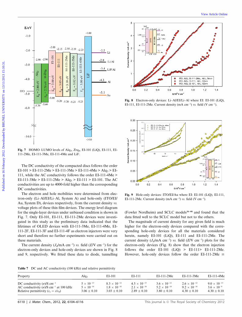
Fig. 7 HOMO–LUMO levels of Alq3, Zrq4, EI-101 (LiQ), EI-111, EI-
111-2Me, EI-111-3Me, EI-111-4Me and LiF.
Fig. 8 Electron-only devices: Li–Al/EI/Li–Al where EI: EI-101 (LiQ),
EI-111, EI-111-2Me. Current density (mA cm�2) vs. field (V cm�1).
Fig. 9 Hole-only devices: ITO/EI/Au where EI: EI-101 (LiQ), EI-111,
EI-111-2Me. Current density (mA cm�2) vs. field (V cm�1).
Publ
ishe
d on
16
Febr
uary
201
2. D
ownl
oade
d by
BR
UN
EL
UN
IVE
RSI
TY
on
13/1
1/20
13 1
5:10
:31.
View Article Online
The DC conductivity of the compacted discs follows the order
EI-101 > EI-111-2Me > EI-111-3Me > EI-111-4Me > Alq3 > EI-
111, while the AC conductivity follows the order EI-111-4Me >
EI-111-3Me > EI-111-2Me > Alq3 > EI-111 > EI-101. The AC
conductivities are up to 4000-fold higher than the corresponding
DC conductivities.
The electron and hole mobilities were determined from elec-
tron-only (Li–Al/EI/Li–Al, System A) and hole-only (ITO/EI/
Au, System D), devices respectively, from the current density vs.
voltage plots of these thin film devices. The energy level diagram
for the single-layer devices under unbiased condition is shown in
Fig. 7. Only EI-101, EI-111, EI-111-2Me devices were investi-
gated in this study as the preliminary data indicated that the
lifetimes of OLED devices with EI-111-3Me, EI-111-4Me, EI-
111-2F, EI-111-3F and EI-111-4F as electron injectors were very
short and therefore no further experiments were carried out on
these materials.
The current density (Jd/mA cm�2) vs. field (E/V cm�1) for the
electron-only devices and hole-only devices are shown in Fig. 8
and 9, respectively. We fitted these data to diode, tunnelling
Table 7 DC and AC conductivity (100 kHz) and relative permittivity
Property Alq3 EI-101
DC conductivity (s)/S cm�1 5 � 10�13 8.3 � 10�12
AC conductivity (s)/S cm�1 at 100 kHz 5 � 10�10 1.8 � 10�10
Relative permittivity (3r ¼ 3/30) 3.06 � 0.10 3.03 � 0.10
6110 | J. Mater. Chem., 2012, 22, 6104–6116
(Fowler Nordheim) and SCLC models36–40 and found that the
data fitted well to the SCLC model but not to the others.
The magnitude of current density for any given field is much
higher for the electron-only devices compared with the corre-
sponding hole-only devices for all the materials considered
herein, namely EI-101 (LiQ), EI-111 and EI-111-2Me. The
current density (Jd/mA cm�2) vs. field (E/V cm�1) plots for the
electron-only devices (Fig. 8) show that the electron injection
follows the order EI-101 (LiQ) > EI-111> EI-111-2Me.
However, hole-only devices follow the order EI-111-2Me $
EI-111 EI-111-2Me EI-111-3Me EI-111-4Me
4.5 � 10�13 3.6 � 10�12 2.6 � 10�12 9.0 � 10�13
2.1 � 10�10 5.2 � 10�10 9.2 � 10�10 3.6 � 10�9
2.89 � 0.10 3.80 � 0.10 4.30 � 0.10 4.30 � 0.10
This journal is ª The Royal Society of Chemistry 2012

Table 8 Thin film conductivity, electron and hole mobilities and charge carrier density
Property Alq3 EI-101 EI-111 EI-111-2Me
Thin film conductivity (S cm�1) from electron-only devices 7.5 � 10�10 3.3 � 10�9 1.8 � 10�9 8.3 � 10�10
Thin film conductivity (S cm�1) from hole-only devices 4.8 � 10�11 1.1 � 10�10 1.4 � 10�10 1.1 � 10�10
Electron mobility (me/cm2 V�1 s�1) from electron-only devices 4.4 � 10�7 3.6 � 10�7 3.1 � 10�7 4.0 � 10�8
Hole mobility (mh/cm2 V�1 s�1) from hole-only devices 1.1 � 10�8 2.1 � 10�9 2.5 � 10�9 1.4 � 10�9
Electron carrier density (ne/cm�3) 1.1 � 1016 5.7 � 1016 3.6 � 1016 1.3 � 1017
Hole carrier density (nh/cm�3) 2.7 � 1016 3.3 � 1017 3.5 � 1017 4.9 � 1017
Fig. 10 Comparison of electron-only devices Li–Al/EI/Li–Al with
Al/EI/Al where EI: EI-101 (LiQ), EI-111, EI-111-2Me.
Publ
ishe
d on
16
Febr
uary
201
2. D
ownl
oade
d by
BR
UN
EL
UN
IVE
RSI
TY
on
13/1
1/20
13 1
5:10
:31.
View Article Online
EI-101 > EI-111 at high fields (E > 5 � 105 V cm�1) and at low
fields they are identical within experimental error.
Thin film conductivity was determined from the Ohmic region
(Jd f V) and the mobility was calculated from the space charge
region (Jd f V2) using the equation:
JSCLC ¼ (9/8)3mV2/d3
where JSCLC ¼ current density in the SCLC region, 3 ¼ permit-
tivity, m ¼ mobility, V ¼ voltage and d ¼ thickness. The data
obtained from the hole-only and electron-only devices are
summarized in Table 8.
There is a significant difference in conductivities of up to 1000-
fold between the vacuum thermal evaporated thin films and the
compacted discs: this is attributed to the morphology and the
nature of packing in the thin films where we expect the molecular
orientation to affect the electrical and electronic properties
(anisotropic conductivity and mobility) compared to the
isotropic packing in the bulk compacted powders.1,45,46
Several features are immediately obvious from Table 8:
(i) The thin film conductivity of EI-101 is higher than that of
EI-111 and EI-111-2Me (EI-101 > EI-111 > EI-111-2Me) for the
electron-only devices. The electron mobility follows the same
order.
(ii) The degree of anisotropy (conductivity of the thin film/
conductivity of the disc) is 4000 for EI-111, 398 for EI-101 and
230 for EI-111-2Me.
(iii) The hole mobilities of all the electron injector materials
studied here are comparable.
The question is whether the reduction in operating voltage by
LiF or LiQ (EI-101) is due to the reaction with the thermally
evaporated reactive aluminium atoms with the lithium
compounds, thereby producing elemental lithium as proposed by
Kido et al.,10,17 where Alq3 is an electron transporter,
3LiF + Al + 3Alq3 / AlF3 + 3Li+Alq3�
If this were true, then any lithium complex should provide
a reduction in the operating voltage as free Li atoms are
produced on reaction with Al, thereby reducing the work func-
tion of the organics (electron transporter)/Al electrode interface.
Thus, we reasoned that single-layer devices made of the
lithium complexes of EI-101 (LiQ), EI-111 and EI-111-2Me with
Li–Al electrodes (System A, Fig. 8) should produce the same
order of current density as for the devices Al/EI/Al (Fig. 10,
System B) for a given field. To test this principle, we fabricated
devices of EI-101, EI-111 and EI-111-2Me having aluminium as
top and bottom contacts by vacuum thermal evaporation (VTE).
First, a relatively thick layer of aluminium (200 nm) was
This journal is ª The Royal Society of Chemistry 2012
evaporated onto ITO/glass, then an electron injector was evap-
orated, followed by aluminium top contact of approximately
200 nm.
Consistent with our expectation, the current density for the
devices with aluminium top and bottom contacts was compa-
rable to that of the devices with Li–Al (top and bottom) contacts.
This clearly indicates that either energetic aluminium atoms, or
surface or energetic lithium complexes on Al, are sufficient to
produce a low work function metal alloy-like (Li–Al type)
behaviour with concomitant lowering of the barrier for injection
of electrons. This is an important finding as it paves the way for
the production of OLEDs with an inverted device structure,
namely starting with an aluminium film electrode onto a silicon
backplane or stainless steel electrode for flexible display appli-
cations. Another possibility is the enhancement of conductivity
as a result of the production of charge transfer complexes of the
type Li+Alq3�.
For our electron injectors, we propose similar reactions
consistent with Li et al.26
Al + 6LiL / AlL3 + 3{Li+(LiL)�_}
To further ascertain that the aluminium on the ITO is indeed
required to produce the low work function contact to the elec-
tron injector, we fabricated devices of the type (ITO/EI/Al,
System C, Fig. 11) to establish that the current density is much
smaller than for system B (Al/EI/Al). Table 9 summarises the
current density at 5 � 105 V cm�1 for all the electrode systems
investigated.
J. Mater. Chem., 2012, 22, 6104–6116 | 6111

Fig. 11 Single-layer mixed-carrier devices: ITO/EI/Al where EI: EI-101
(LiQ), EI-111, EI-111-2Me.
Fig. 13 Current density–voltage–luminance characteristics of ITO/
ZnTPTP (20 nm)/a-NPB (50 nm)/Alq3 : DPQA (40 : 0.1 nm)/Zrq4(20 nm)/EI (1 nm)/Al where EI: LiF, EI-101 (LiQ), EI-111, EI-111-2Me.
Fig. 12 HOMO–LUMO energy levels for ZnTPTP (hole injector),
a-NPB (hole transporter), Alq3 (host), DPQA (---- green dopant), Zrq4(electron transporter), EI (electron injector) where EI: EI-101 (LiQ),
EI-111, EI-111-2Me.
Publ
ishe
d on
16
Febr
uary
201
2. D
ownl
oade
d by
BR
UN
EL
UN
IVE
RSI
TY
on
13/1
1/20
13 1
5:10
:31.
View Article Online
The current density of Al/EI/Al is either higher than or
comparable to Li–Al/EI/Li–Al, confirming the fact that Li is
produced at the interface as suggested by Kido et al.10,17
We fabricated mixed-carrier single-layer devices of ITO/EI/Al.
At low field (E < 1� 106 V cm�1), the Jd follows the order EI-101
> EI-111-2Me > EI-111 whilst at high field (E > 1.5 � 106 V
cm�1), the order of current injection changes to EI-111-2Me >
EI-111 > EI-101. The current densities of the ITO/EI/Al devices
(dual carrier transport) are higher than those of the hole-only
devices, namely, ITO/EI/Au as expected.
Green devices. Green devices of ITO (40 U per square)/
ZnTPTP (20 nm)//a-NPB (50 nm)/Alq3 : DPQA (40 nm :
0.1 nm)/Zrq4 (20 nm)/EI (1 nm)/Al were fabricated using the
Solciet OLED Pilot Plant equipment purchased from ULVAC,
Japan. The energy level diagram for the device under zero bias is
depicted in Fig. 13.
The current density (Jd) vs. voltage (V) plots (Fig. 12) show
that the EI-111 has the highest current injection followed by EI-
111-2Me, EI-101 and LiF (EI-111 > EI-111-2Me > EI-101 > LiF)
despite the fact that the electron-only single-layer devices show
that the current injection is highest for EI-101 (Fig. 8). We
explain this difference on the basis that these multilayer light
emitting devices are operating under mixed-carrier conduction
and the interface between the Zrq4 and the electron injector
would have substantial influence. We postulate that there is also
the possibility of the formation of a charge transfer complex of
formula Li+(Zrq4L)� which could act as a dipole just like LiF
on diamond21 and thus enhance carrier injection. The luminance
(L/cd m�2) vs. voltage (Fig. 13) simply follows the same pattern as
Table 9 Current density at a field of 5 � 105 V cm�1 for electron-only and h
System Anode (W.F./eV) Cathode (W.F./eV) EI-101 (LiQ
A Li–Al (�2.8) Li–Al (�2.8) 2.5 � 0.1B Al (�4.3) Al (�4.3) 4.0 � 0.1C ITO (�4.8) Al (�4.3) 0.24 � 0.02D ITO (�4.8) Au (�5.1) 0.06 � 0.02
6112 | J. Mater. Chem., 2012, 22, 6104–6116
the Jd vs. V. The electroluminescence spectra are shown in
Fig. 14. The slight differences in the spectra and the consequent
colour co-ordinates are attributed to minor variation in the
dopant concentration. The turn-on voltages (to give a luminance
of 1 cd m�2) for EI-111, EI-111-2Me, EI-101 and LiF are 3.0, 3.2,
ole-only devices
) Jd/mA cm�2 EI-111 Jd/mA cm�2 EI-111-2Me Jd/mA cm�2
1.7 � 0.1 1.0 � 0.11.4 � 0.1 1.0 � 0.10.12 � 0.02 0.11 � 0.020.06 � 0.02 0.06 � 0.02
This journal is ª The Royal Society of Chemistry 2012
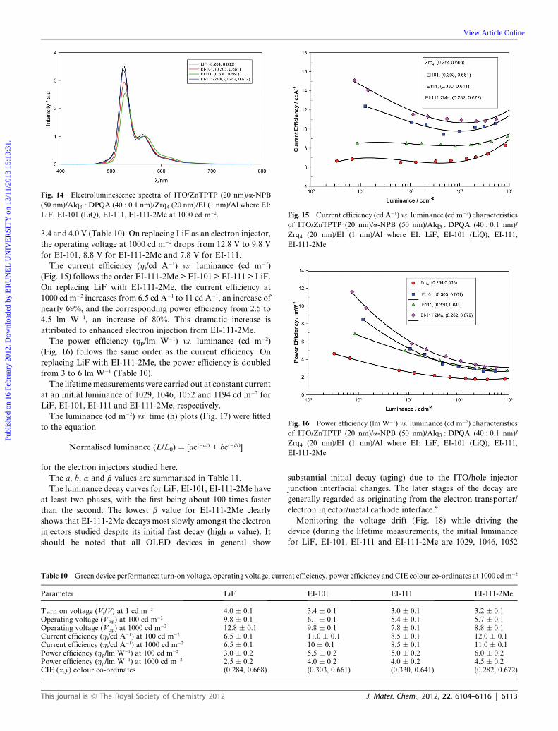
Fig. 14 Electroluminescence spectra of ITO/ZnTPTP (20 nm)/a-NPB
(50 nm)/Alq3 : DPQA (40 : 0.1 nm)/Zrq4 (20 nm)/EI (1 nm)/Al where EI:
LiF, EI-101 (LiQ), EI-111, EI-111-2Me at 1000 cd m�2. Fig. 15 Current efficiency (cd A�1) vs. luminance (cd m�2) characteristics
of ITO/ZnTPTP (20 nm)/a-NPB (50 nm)/Alq3 : DPQA (40 : 0.1 nm)/
Zrq4 (20 nm)/EI (1 nm)/Al where EI: LiF, EI-101 (LiQ), EI-111,
EI-111-2Me.
Fig. 16 Power efficiency (lm W�1) vs. luminance (cd m�2) characteristics
of ITO/ZnTPTP (20 nm)/a-NPB (50 nm)/Alq3 : DPQA (40 : 0.1 nm)/
Zrq4 (20 nm)/EI (1 nm)/Al where EI: LiF, EI-101 (LiQ), EI-111,
EI-111-2Me.
Publ
ishe
d on
16
Febr
uary
201
2. D
ownl
oade
d by
BR
UN
EL
UN
IVE
RSI
TY
on
13/1
1/20
13 1
5:10
:31.
View Article Online
3.4 and 4.0 V (Table 10). On replacing LiF as an electron injector,
the operating voltage at 1000 cd m�2 drops from 12.8 V to 9.8 V
for EI-101, 8.8 V for EI-111-2Me and 7.8 V for EI-111.
The current efficiency (hi/cd A�1) vs. luminance (cd m�2)
(Fig. 15) follows the order EI-111-2Me > EI-101 > EI-111 > LiF.
On replacing LiF with EI-111-2Me, the current efficiency at
1000 cd m�2 increases from 6.5 cd A�1 to 11 cd A�1, an increase of
nearly 69%, and the corresponding power efficiency from 2.5 to
4.5 lm W�1, an increase of 80%. This dramatic increase is
attributed to enhanced electron injection from EI-111-2Me.
The power efficiency (hp/lm W�1) vs. luminance (cd m�2)
(Fig. 16) follows the same order as the current efficiency. On
replacing LiF with EI-111-2Me, the power efficiency is doubled
from 3 to 6 lm W�1 (Table 10).
The lifetimemeasurements were carried out at constant current
at an initial luminance of 1029, 1046, 1052 and 1194 cd m�2 for
LiF, EI-101, EI-111 and EI-111-2Me, respectively.
The luminance (cd m�2) vs. time (h) plots (Fig. 17) were fitted
to the equation
Normalised luminance (L/L0) ¼ [ae(�at) + be(�bt)]
for the electron injectors studied here.
The a, b, a and b values are summarised in Table 11.
The luminance decay curves for LiF, EI-101, EI-111-2Me have
at least two phases, with the first being about 100 times faster
than the second. The lowest b value for EI-111-2Me clearly
shows that EI-111-2Me decays most slowly amongst the electron
injectors studied despite its initial fast decay (high a value). It
should be noted that all OLED devices in general show
Table 10 Green device performance: turn-on voltage, operating voltage, curre
Parameter LiF
Turn on voltage (Vt/V) at 1 cd m�2 4.0 � 0.1Operating voltage (Vop) at 100 cd m�2 9.8 � 0.1Operating voltage (Vop) at 1000 cd m�2 12.8 � 0.1Current efficiency (hi/cd A�1) at 100 cd m�2 6.5 � 0.1Current efficiency (hi/cd A�1) at 1000 cd m�2 6.5 � 0.1Power efficiency (hp/lm W�1) at 100 cd m�2 3.0 � 0.2Power efficiency (hp/lm W�1) at 1000 cd m�2 2.5 � 0.2CIE (x,y) colour co-ordinates (0.284, 0.668)
This journal is ª The Royal Society of Chemistry 2012
substantial initial decay (aging) due to the ITO/hole injector
junction interfacial changes. The later stages of the decay are
generally regarded as originating from the electron transporter/
electron injector/metal cathode interface.9
Monitoring the voltage drift (Fig. 18) while driving the
device (during the lifetime measurements, the initial luminance
for LiF, EI-101, EI-111 and EI-111-2Me are 1029, 1046, 1052
nt efficiency, power efficiency and CIE colour co-ordinates at 1000 cd m�2
EI-101 EI-111 EI-111-2Me
3.4 � 0.1 3.0 � 0.1 3.2 � 0.16.1 � 0.1 5.4 � 0.1 5.7 � 0.19.8 � 0.1 7.8 � 0.1 8.8 � 0.111.0 � 0.1 8.5 � 0.1 12.0 � 0.110 � 0.1 8.5 � 0.1 11.0 � 0.15.5 � 0.2 5.0 � 0.2 6.0 � 0.24.0 � 0.2 4.0 � 0.2 4.5 � 0.2(0.303, 0.661) (0.330, 0.641) (0.282, 0.672)
J. Mater. Chem., 2012, 22, 6104–6116 | 6113
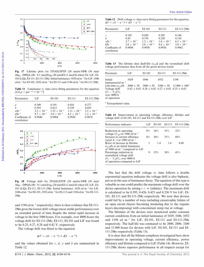
Fig. 17 Lifetime plots for ITO/ZnTPTP (20 nm)/a-NPB (50 nm)/
Alq3 : DPQA (40 : 0.1 nm)/Zrq4 (20 nm)/EI (1 nm)/Al where EI: LiF, EI-
101 (LiQ),EI-111,EI-111-2Me. Initial luminance: 1029 cdm�2 forLiF, 1046
cdm�2 for EI-101, 1052 cdm�2 for EI-111 and 1194 cdm�2 for EI-111-2Me.
Table 12 Drift voltage vs. time curve fitting parameters for the equation,DV ¼ c(1 � e�gt) + d(1 � e�dt)
Parameters LiF EI-101 EI-111 EI-111-2Me
c 0.145 0.050 0.203 0.146d 0.45 0.376 0.220 0.110g/h�1 5.7 � 10�3 1.2 � 10�3 1.0 � 10�3 6.3 � 10�3
d/h�1 2.0 � 10�4 2.0 � 10�4 8.6 � 10�5 5.0 � 10�4
Coefficient ofcorrelation
0.9894 0.9930 0.9956 0.9942
Table 13 The lifetime data [half-life (t1/2)] and the normalised driftvoltage performance data from all the green devices tested
Parameter LiF EI-101 EI-111 EI-111-2Me
Initialluminance/cd m�2
1029 1046 1052 1194
Life-time (t1/2)/h 2000 � 50 2800 � 50 3200 � 50 12 000 � 100a
Voltage drift(Vt � Vo)/V0
over 4000 hof operation
0.42 � 0.02 0.28 � 0.02 0.27 � 0.02 0.25 � 0.02
a Extrapolated value.
Table 14 Improvement in operating voltage, efficiency, lifetime andvoltage drift of EI-101, EI-111 and EI-111-2Me over LiF
Performance indicator LiF EI-101 EI-111 EI-111-2Me
Reduction in operatingvoltage (Vop) at 1000 cd m�2
0% 16% 31% 22%
Increase in current efficiency(hi/cd A�1) at 1000 cd m�2
0% 54% 31% 69%
Ratio of increase in lifetime(t1/2)/h at an initial luminanceof 1000 cd m�2 compared to LiF
1 1.4 1.6 6.00
Percentage reduction innormalised voltage drift(Vt � Vo)/Vo over 4000 hof operation compared to LiF
0 33% 36% 41%
Table 11 Luminance vs. time curve fitting parameters for the equation(L/L0) ¼ [ae(�at) + be(�bt)]
Parameters LiF EI-101 EI-111 EI-111-2Me
a 0.390 0.191 0.416 0.277b 0.593 0.812 0.539 0.695a/h�1 2.2 � 10�3 1.52 � 10�2 1.11 � 10�3 2.5 � 10�3
b/h�1 9.7 � 10�5 2.0 � 10�4 4.2 � 10�5 1.2 � 10�5
Coefficient ofcorrelation
0.9946 0.9904 0.9920 0.9878
Fig. 18 Voltage drift for ITO/ZnTPTP (20 nm)/a-NPB (50 nm)/
Alq3 : DPQA (40 : 0.1 nm)/Zrq4 (20 nm)/EI (1 nm)/Al where EI: LiF, EI-
101 (LiQ), EI-111, EI-111-2Me. Initial luminance: 1029 cd m�2 for LiF,
1046 cdm�2 forEI-101, 1052 cdm�2 forEI-111and 1194 cdm�2 forEI-111-
2Me.
Publ
ishe
d on
16
Febr
uary
201
2. D
ownl
oade
d by
BR
UN
EL
UN
IVE
RSI
TY
on
13/1
1/20
13 1
5:10
:31.
View Article Online
and 1194 cd m�2 respectively), there is clear evidence that EI-111-
2Me gives the lowest drift voltage (most stable performance) over
an extended period of time despite the initial rapid increase in
voltage in the first 1000 hours. For example, over 4000 hours the
voltage drift for EI-111-2Me, EI-111, EI-101 and LiF was found
to be 0.25, 0.27, 0.28 and 0.42 V, respectively.
The voltage drift was fitted to the equation
DV ¼ c(1 � e�gt) + d(1 � e�dt)
and the values obtained for c, d, g and d are summarised in
Table 12.
6114 | J. Mater. Chem., 2012, 22, 6104–6116
The fact that the drift voltage vs. time follows a double
exponential equation indicates the voltage drift is also biphasic,
just as in the case of luminance decay. The equation of this type is
valuable as one could predict the maximum voltage drift over the
device operation by setting t ¼ N (infinity). The maximum drift
is calculated to be 0.595, 0.426, 0.423 and 0.256 V for LiF, EI-
101, EI-111 and EI-111-2Me respectively. We note that devices
could fail by a number of ways including catastrophic failure of
an open circuit (layers becoming insulating due to the organic
layers decomposing) with concomitant steep rise in voltage.
The lifetimes of the devices were monitored under constant
current conditions from an initial luminance of 1029, 1046, 1052
and 1194 cd m�2 for LiF, EI-101, EI-111 and EI-111-2Me
respectively. The half-life was estimated to be 2000, 2800, 3200
and 12 000 hours for devices with LiF, EI-101, EI-111 and EI-
111-2Me respectively (Table 13).
It is clear that all the lithium complexes investigated here show
improvements in operating voltage, current efficiency, power
efficiency and lifetime compared to LiF (Table 14). However, EI-
111-2Me shows superior performance in all respects except for
This journal is ª The Royal Society of Chemistry 2012
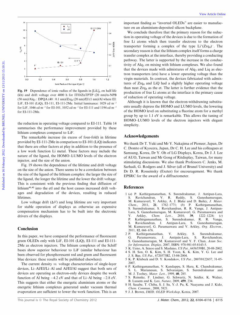
Fig. 19 Dependence of ionic radius of the ligands in [LiL]n on half-life
(kh) and drift voltage over 4000 h for ITO/ZnTPTP (20 nm)/a-NPB
(50 nm)/Alq3 : DPQA (40 : 0.1 nm)/Zrq4 (20 nm)/EI (1 nm)/Al where EI:
LiF, EI-101 (LiQ), EI-111, EI-111-2Me. Initial luminance: 1029 cd m�2
for LiF, 1046 cd m�2 for EI-101, 1052 cd m�2 for EI-111 and 1194 cd m�2
for EI-111-2Me.
Publ
ishe
d on
16
Febr
uary
201
2. D
ownl
oade
d by
BR
UN
EL
UN
IVE
RSI
TY
on
13/1
1/20
13 1
5:10
:31.
View Article Online
the reduction in operating voltage compared to EI-111. Table 14
summarises the performance improvement provided by these
lithium complexes compared to LiF.
The remarkable increase (in excess of four-fold) in lifetime
provided by EI-111-2Me in comparison to EI-101 (LiQ) indicates
that there are other factors at play in addition to the presence of
a low work function Li metal. These factors may include the
nature of the ligand, the HOMO–LUMO levels of the electron
injector, and the size of the anion.
Fig. 19 shows the dependence of the lifetime and drift voltage
on the size of the anion. There seems to be a correlation between
the size of the ligand of the lithium complex: the larger the size of
the ligand, the longer the lifetime and the lower the drift voltage.
This is consistent with the previous finding that diffusion of
lithium41,42 into the etl and the host causes increased drift volt-
ages and degradation of the devices, resulting in reduced
lifetimes.
Low voltage drift (DV) and long lifetime are very important
for stable operation of displays as otherwise an expensive
compensation mechanism has to be built into the electronic
drivers of the displays.
Conclusion
In this paper, we have compared the performance of fluorescent
green OLEDs only with LiF, EI-101 (LiQ), EI-111 and EI-111-
2Me as electron injectors. The lithium complexes of the Schiff
bases show superior behaviour to LiF (similar behaviour has
been observed for phosphorescent red and green and fluorescent
blue devices: these results will be published elsewhere).
The current density vs. voltage characteristics of single-layer
devices, Li–Al/EI/Li–Al and Al/EI/Al suggest that both sets of
devices are operating as electron-only devices despite the work
function of Al being �4.2 eV and that of Li–Al being �2.8 eV.
This suggests that either the energetic aluminium atoms or the
energetic lithium complexes generated under vacuum thermal
evaporation are sufficient to lower the work function. This is an
This journal is ª The Royal Society of Chemistry 2012
important finding as ‘‘inverted OLEDs’’ are easier to manufac-
ture on an aluminium-deposited silicon backplane.
We conclude therefore that the primary reason for the reduc-
tion in operating voltage of the devices is due to the formation of
free Li atoms which then transfer electrons to the electron
transporter forming a complex of the type Li+(Zrq4)�. The
secondary reason is that the lithium complex itself forms a charge
transfer complex at the interface, thereby providing a conducting
pathway. The latter is supported by the increase in the conduc-
tivity of Alq3 on mixing with lithium complexes. We also found
that the devices made with admixtures of Alq3 and Liq as elec-
tron transporters (ets) have a lower operating voltage than the
virgin materials. In contrast, the devices fabricated with admix-
tures of Zrq4 and LiQ had a slightly higher operating voltage
than neat Zrq4 as the et. The latter is further evidence that the
production of free Li atoms at the interface is the primary cause
of reduction of operating voltage.
Although it is known that the electron-withdrawing substitu-
ents usually depress the HOMO and LUMO levels, the lowering
of the HOMO level on substituting a fluorine atom for a methyl
group by up to 1.1 eV is remarkable. This allows the tuning of
HOMO–LUMO levels of the electron injectors with elegant
simplicity.
Acknowledgements
We thankDr T. Yuki andMrY. Nakajima of Pioneer, Japan, Dr
C. Domto of Kyocera, Japan, Dr C. H. Lee and his colleagues at
Samsung, Korea, Dr Y. Oh of LG Displays, Korea, Dr J. J. Lee
of AUO, Taiwan and Mr Gong of Ritdisplay, Taiwan, for many
stimulating discussions. We also thank Professors C. Jenks, M.
Sarhadi, G. Rodgers and J. Silver (all of Brunel University) and
Dr D. R. Rosseinsky (Exeter) for encouragement. We thank
EPSRC for the award of a diffractometer.
References
1 (a) P. Kathirgamanathan, S. Surendrakumar, J. Antipan-Lara,S. Ravichandran, V. R. Reddy, S. Ganeshamurugan,M. Kumaraverl, V. Arkley, A. J. Blake and D. Bailey, J. Mater.Chem., 2011, 21, 1762–1771; (b) P. Kathirgamanathan,S. Surendrakumar, S. Ravichandran, R. R. Vanga, J. Antipan-Lara, S. Ganeshamurugan, M. Kumaraverl, G. Paramaswara andV. Arkley, Chem. Lett., 2010, 39, 1222–1224; (c)P. Kathirgamanathan, S. Surendrakumar, R. R. Vanga,S. Ravichandran, J. Antipan-Lara, S. Ganeshamurugan,M. Kumaraverl, G. Paramaswara and V. Arkley, Org. Electron.,2011, 12, 666–676.
2 P. Kathirgamanathan, V. Arkley, S. Surendrakumar,G. Paramaswara, J. Antip�an-Lara, S. Ravichandran,S. Ganeshamurugan, M. Kumaraverl and Y. F. Chan, Asian Soc.for Information. Display, 2007, ISBN: 978-981-05-8143-5.
3 K. Ueno, A. Senoo and S. Mashmo,US Pat., 6436559B1, 20-08-2002.4 S. H. Son, O. K. Kim, S. H. Yoon, K. K. Kim, Y. G. Lee andJ. S. Bae, US Pat., 6720573B2, 13-04-2004.
5 K. P. Klubeck and D. Y. Kondakov, US Pat., 2007/0122657, 31-05-2007.
6 P. Kathirgamanathan, V. Kandappu, S. Hara, K. Chandrakumar,S. L. Marianesan, S. Selvaranjan, S. Surendrakumar andM. J. Toohey, Mater. Lett., 1999, 40, 285.
7 S. Reinnke, F. Lindner, G. Schwartz, N. Seidler, K. Walzer,B. Lussem and K. Leo, Nature, 2009, 459, 234.
8 H. Sasabe, T. Chiba, S. J. Su, Y.-J. Pu, K. Naayama and J. Kido,Chem. Commun., 2008, 5821.
9 J. J. Brown, IMID, OLED Workshop, Korea, 2007.
J. Mater. Chem., 2012, 22, 6104–6116 | 6115
Publ
ishe
d on
16
Febr
uary
201
2. D
ownl
oade
d by
BR
UN
EL
UN
IVE
RSI
TY
on
13/1
1/20
13 1
5:10
:31.
View Article Online
10 J. Endo, T. Matsumoto and J. Kido, Jpn. J. Appl. Phys., 2002, 41,L358.
11 I. D. Parker, J. Appl. Phys., 1994, 75, 1656.12 A. J. Heeger, I. D. Parker and Y. Yang, Synth. Met., 1994, 67, 23.13 R. Partridge, US Pat., 1976/3995299, 1976.14 C. W. Tang, US Pat., 1982/4356429, 1982.15 C. W. Tang and S. A. Van Slyke, Appl. Phys. Lett., 1987, 51, 913.16 J. H. Burroughes, D. D. C. Bradley, A. R. Brown, R. N. Marks,
K. Mackay, R. H. Friend, P. L. Burn and A. B. Holmes, Nature,1990, 347, 539.
17 J. Kido, K. Nagai and Y. Okamoto, IEEE Trans. Electron Devices,1997, 44, 1245.
18 T. Wakimoto, Y. Fukuda, K. Nagayama, A. Yokoi, H. Nakada andM. Tsuchida, IEEE Trans. Electron Devices, 1997, 44, 1245.
19 L. S. Hung, C.W. Tang andM.G.Mason,Appl. Phys. Lett., 1997, 70,152.
20 C. I. Wu, G. R. Lee and T. W. Pi, Appl. Phys. Lett., 2005, 87, 212108.21 K. W. Wong, Y. M. Wang, S. T. Lee and R. W. M. Kwok, Diamond
Relat. Mater., 1999, 8, 1885.22 P. Kathirgamanathan, Eur Pat., 1458834, 2000.23 W. J. Begley and M. Rajeswaran, Acta Crystallogr., Sect. E: Struct.
Rep. Online, 2006, 62, m200.24 M. Rajeswaran, W. J. Begley, L. O. Olson and S. Huo, Polyhedron,
2007, 26, 3653.25 E. Bohm, C. Pflumm, F. Voges, M. Flammich, H. Heil, A. Busing,
A. Parham, R. Fortte and T. Mujica, IDW Proceedings, 2009, p. 431.26 Y. Li, D. Zhang, L. Duan, R. Zhang, L. Wang, J. Qiao and Y. Qiu,
Jpn. J. Appl. Phys., 2006, 45, L1253.27 P. Kathirgamanathan, V. Arkley, S. Surendrakumar, Y. F. Chan,
S. Ravichandran, S. Ganeshamurugan, M. Kumaraverl, J. Antipan-Lara, G. Paramaswara and V. R. Reddy, Dig. Tech. Pap. - Soc. Inf.Disp. Int. Symp., 2010, 32.2, 465.
28 Y. J. Pu, M. Miyamoto, K. Nakayama, T. Oyama, Y. Masaaki andJ. Kido, Org. Electron., 2009, 10, 228.
29 S. G. Schulman and M. S. Rietta, Anal. Chem., 1971, 60, 1762.30 P. Kathirgamanathan and G. Paramaswara, unpublished work,
carried out by Huntingdon Life Sciences under contract.31 B. N. Ames, J. MCCann and E. Yamasaki,Mutat. Res., 1975, 31, 347.
6116 | J. Mater. Chem., 2012, 22, 6104–6116
32 D. M. Maron and B. N. Ames, Mutat. Res., 1983, 113, 173–215.33 X. Sun, D. Y. Zhou, L. Qiu, L. S. Lao and F. Yan, J. Phys. Chem. C,
2011, 115, 2433.34 Y. Kim, Nanotechnology, 2008, 19, 355207.35 P. Kathirgamanathan and D. R. Rosseinsky, J. Chem. Soc., Chem.
Commun., 1980, 839.36 (a) P. Kathirgamanathan, US Pat., 2005/0106412 A1, 2005; (b)
P. Kathirgamanathan, S. Surendrakumar and Y. F. Chan, US Pat.,2011/0108819A1, 2011.
37 M. Cole and W. Brutting, Physics of Organic Semiconductors, Wiley-VCH Verlag GmBH, 2005, pp. 95–128, ISBN-13: 978-3-527-40550-3.
38 A. J. Heeger, I. D. Parker and Y. Yang, Synth. Met., 1994, 67, 23.39 J. Antip�an-Lara and P. Kathirgamanathan, IEE Proc.: Optoelectron.,
2000, 147, 369.40 M. A. Lampert and P. Mark, Current Injection in Solids, Academic
Press, New York, 1970, ISBN: 75-117115.41 C. K. Tzen, W. J. Shen, Y. L. Kao and S. J. Tang, IDW/AD’05,
Sunport Takamatsu, Japan, Proceedings of the 12th InternationalDisplay Workshops in Conjunction with Asia Display, 2005, p. 621.
42 S. Madhusoodhanan, E. Polikarpov, S. Garon and M. E. Thompson,Proceedings of the International Symposium Super FunctionalityOrganic Devices, IPAP Conf. Series 6, pp. 110–113, 2009.
43 P. Kathirgamanathan and Y. F. Chan, PCT WO 2008/081178, 2008.44 (a) J. Bredas and A. Heeger, Chem. Phys. Lett., 1994, 217, 507; (b)
D. R. Baigent, N. C. Greenham, J. Grunner, R. N. Marks,R. H. Friend, S. C. Moratti and A. R. Holmes, Synth. Met., 1994,67(1–3), 3.
45 P. Kathirgamanathan, M. A. Mazid and D. R. Rosseinsky, J. Chem.Soc., Perkin Trans. 2, 1982, 593.
46 P. Kathirgamanathan, High Value Polymers, Special Publication No:87, Royal Society of Chemistry, 1991, pp. 174–205, ISBN 0-85186-867-3.
47 L. B. Valdes, Proc. IRE, 1954, 42, 420.48 L. J. Van der Pauw, Philips Res. Rep., 1958, 13, 1.49 L. J. van der Pauw, Philips Tech. Rev., 1959, 20, 220.50 L. J. Van der Pauw, Philips Res. Rep., 1961, 16, 187.51 P. Kathirgamanathan, PhD thesis, Exeter, 1980.
This journal is ª The Royal Society of Chemistry 2012